artix-7 fpga development board ac7a035 system on module
TRANSCRIPT
ARTIX-7 FPGA Development Board
AC7A035 System on Module

ARTIX-7 FPGA Development Board AC7A035 User Manual
2 / 29
Amazon Store: https://www.amazon.com/alinx
Version Record
Version Date Release By Description
Rev 1.0 2020-06-28 Rachel Zhou First Release
ARTIX-7 FPGA Development Board AC7A035 User Manual
3 / 29
Amazon Store: https://www.amazon.com/alinx
Table of Contents
Version Record ......................................................................................... 2
Part 1: AC7A035 Core Board Introduction ................................................ 4
Part 2: FPGA Chip .................................................................................... 6
Part 3: Active Differential Crystal .............................................................. 8
Part 3.1: 200Mhz Active Differential clock ........................................... 8
Part 3.2: 125MHz Active Differential Crystal ....................................... 9
Part 4: DDR3 DRAM .............................................................................. 10
Part 5: QSPI Flash ................................................................................. 13
Part 6: LED Light on Core Board ............................................................ 15
Part 7: JTAG Interface ............................................................................. 17
Part 8: Power Interface on the Core Board ............................................. 18
Part 9: Board to Board Connectors pin assignment ................................ 18
Part 10: Power Supply ............................................................................ 26
Part 11: Size Dimension ......................................................................... 29
ARTIX-7 FPGA Development Board AC7A035 User Manual
4 / 29
Amazon Store: https://www.amazon.com/alinx
Part 1: AC7A035 Core Board Introduction
AC7A035 (core board model, the same below) FPGA core board, it is
based on XILINX's ARTIX-7 series 35T XC7A35T-2FGG484I. It is a
high-performance core board with high speed, high bandwidth and high
capacity. It is suitable for high-speed data communication, video image
processing, high-speed data acquisition etc.
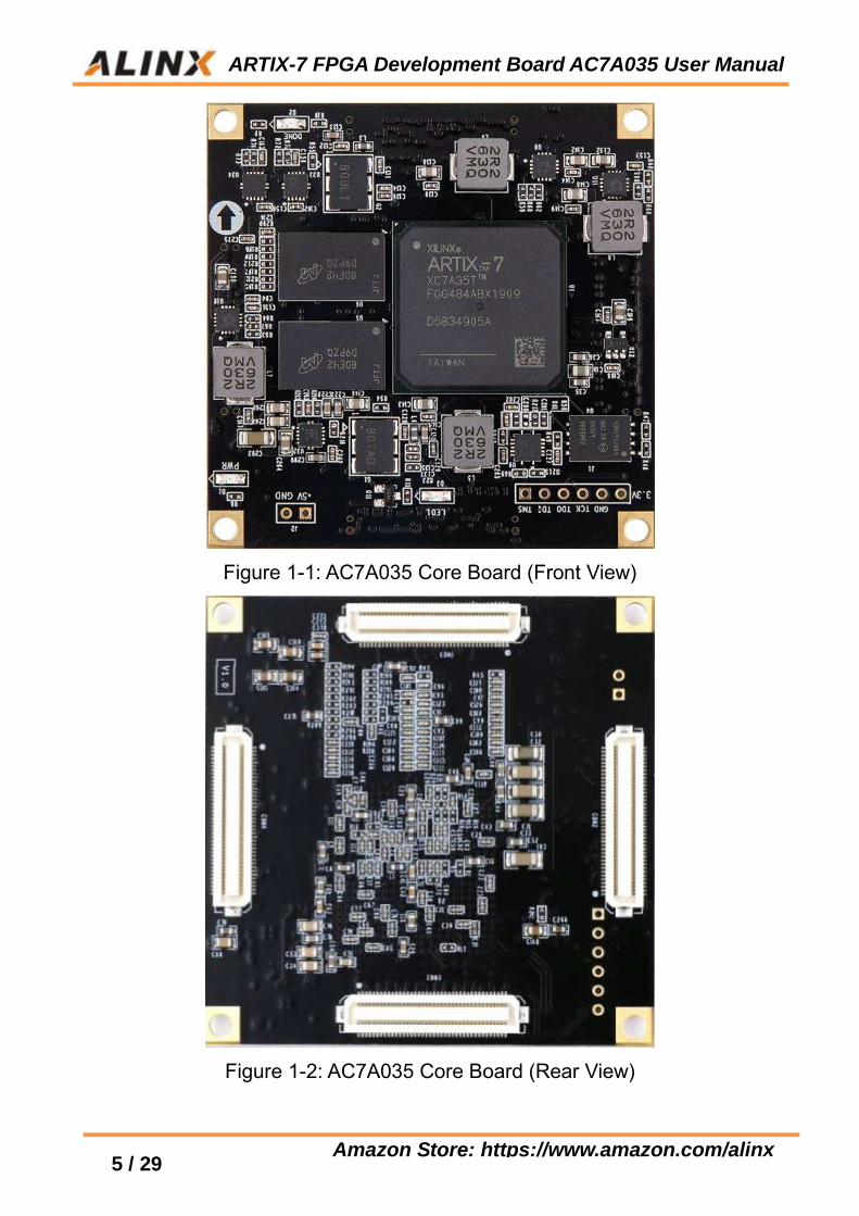
This AC7A200 core board uses two pieces of MICRON's
MT41J256M16HA-125 DDR3 chip, each DDR has a capacity of 4Gbit; two
DDR chips are combined into a 32-bit data bus width, and the read/write data
bandwidth between FPGA and DDR3 is up to 25Gb; such a configuration can
meet the needs of high bandwidth data processing.
The AC7A035 core board expands 180 standard IO ports of 3.3V level, 15
standard IO ports of 1.5V level, and 4 pairs of GTP high speed RX/TX
differential signals. For users who need a lot of IO, this core board will be a
good choice. Moreover, the routing between the FPGA chip and the interface is
equal length and differential processing, and the core board size is only 2.36
inch *2.36 inch, which is very suitable for secondary development.
ARTIX-7 FPGA Development Board AC7A035 User Manual
5 / 29
Amazon Store: https://www.amazon.com/alinx
Figure 1-1: AC7A035 Core Board (Front View)
Figure 1-2: AC7A035 Core Board (Rear View)
ARTIX-7 FPGA Development Board AC7A035 User Manual
6 / 29
Amazon Store: https://www.amazon.com/alinx
Part 2: FPGA Chip
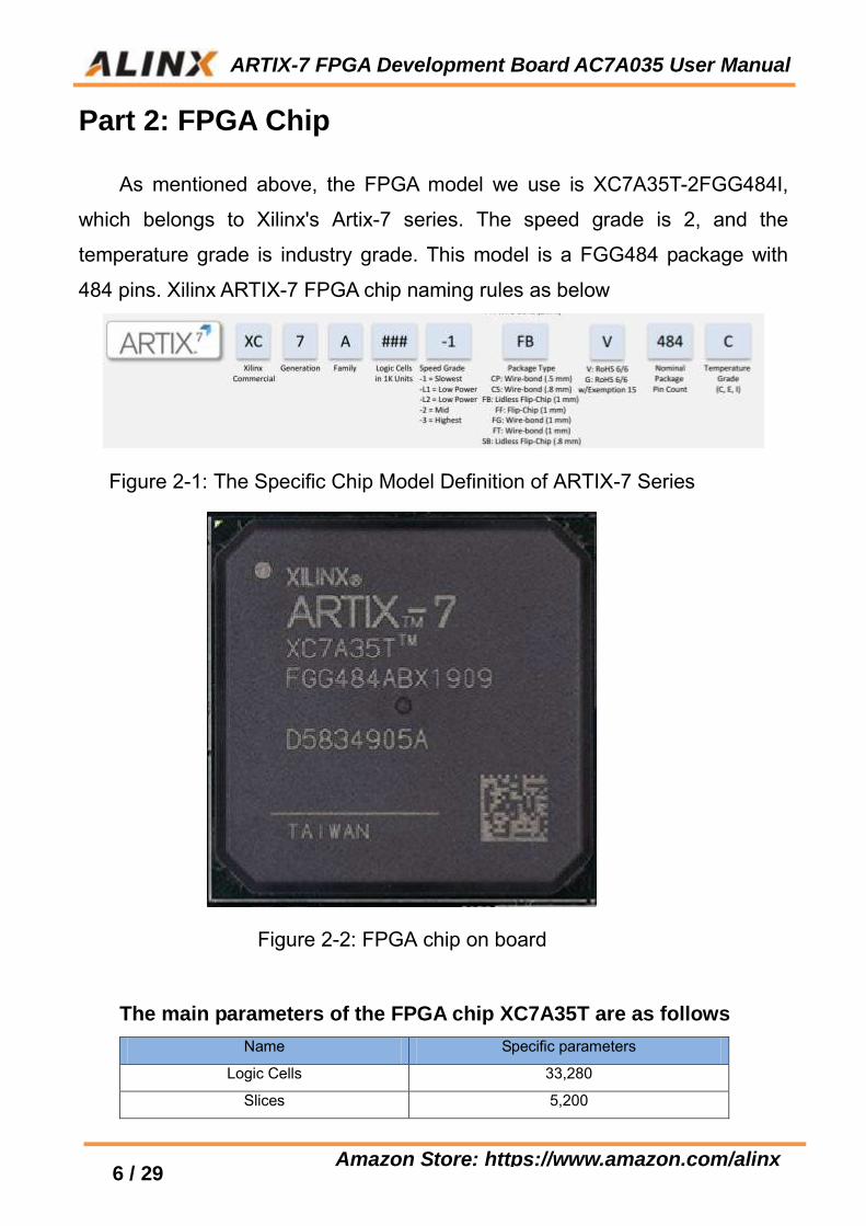
As mentioned above, the FPGA model we use is XC7A35T-2FGG484I,
which belongs to Xilinx's Artix-7 series. The speed grade is 2, and the
temperature grade is industry grade. This model is a FGG484 package with
484 pins. Xilinx ARTIX-7 FPGA chip naming rules as below
Figure 2-1: The Specific Chip Model Definition of ARTIX-7 Series
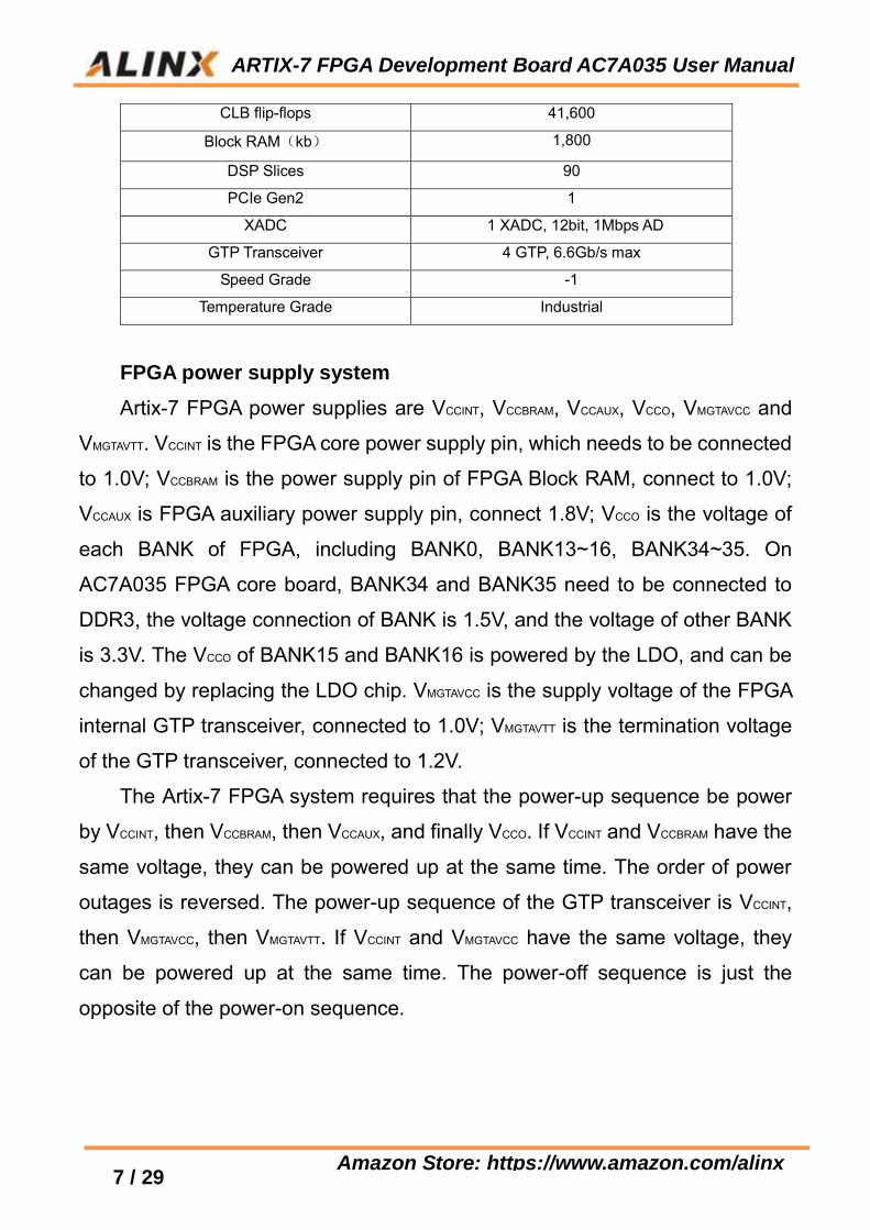
Figure 2-2: FPGA chip on board
The main parameters of the FPGA chip XC7A35T are as follows
Name Specific parameters
Logic Cells 33,280
Slices 5,200
ARTIX-7 FPGA Development Board AC7A035 User Manual
7 / 29
Amazon Store: https://www.amazon.com/alinx
CLB flip-flops 41,600
Block RAM(kb) 1,800
DSP Slices 90
PCIe Gen2 1
XADC 1 XADC, 12bit, 1Mbps AD
GTP Transceiver 4 GTP, 6.6Gb/s max
Speed Grade -1
Temperature Grade Industrial
FPGA power supply system
Artix-7 FPGA power supplies are VCCINT, VCCBRAM, VCCAUX, VCCO, VMGTAVCC and
VMGTAVTT. VCCINT is the FPGA core power supply pin, which needs to be connected
to 1.0V; VCCBRAM is the power supply pin of FPGA Block RAM, connect to 1.0V;
VCCAUX is FPGA auxiliary power supply pin, connect 1.8V; VCCO is the voltage of
each BANK of FPGA, including BANK0, BANK13~16, BANK34~35. On
AC7A035 FPGA core board, BANK34 and BANK35 need to be connected to
DDR3, the voltage connection of BANK is 1.5V, and the voltage of other BANK
is 3.3V. The VCCO of BANK15 and BANK16 is powered by the LDO, and can be
changed by replacing the LDO chip. VMGTAVCC is the supply voltage of the FPGA
internal GTP transceiver, connected to 1.0V; VMGTAVTT is the termination voltage
of the GTP transceiver, connected to 1.2V.
The Artix-7 FPGA system requires that the power-up sequence be power
by VCCINT, then VCCBRAM, then VCCAUX, and finally VCCO. If VCCINT and VCCBRAM have the
same voltage, they can be powered up at the same time. The order of power
outages is reversed. The power-up sequence of the GTP transceiver is VCCINT,
then VMGTAVCC, then VMGTAVTT. If VCCINT and VMGTAVCC have the same voltage, they
can be powered up at the same time. The power-off sequence is just the
opposite of the power-on sequence.
ARTIX-7 FPGA Development Board AC7A035 User Manual
8 / 29
Amazon Store: https://www.amazon.com/alinx
Part 3: Active Differential Crystal
The AC7A035 core board is equipped with two Sitime active differential
crystals, one is 200MHz, the model is SiT9102-200.00MHz, the system main
clock for FPGA and used to generate DDR3 control clock; the other is 125MHz,
model is SiT9102 -125MHz, reference clock input for GTP transceivers.
Part 3.1: 200Mhz Active Differential clock
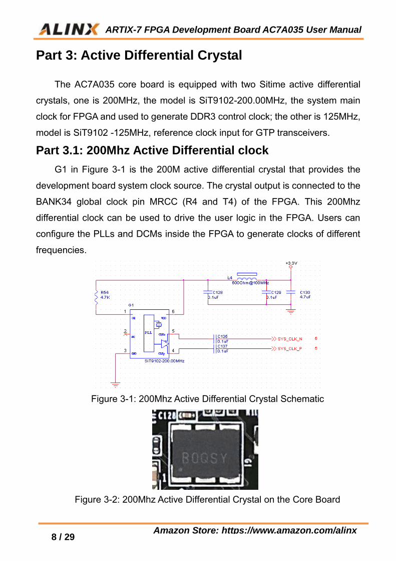
G1 in Figure 3-1 is the 200M active differential crystal that provides the
development board system clock source. The crystal output is connected to the
BANK34 global clock pin MRCC (R4 and T4) of the FPGA. This 200Mhz
differential clock can be used to drive the user logic in the FPGA. Users can
configure the PLLs and DCMs inside the FPGA to generate clocks of different
frequencies.
Figure 3-1: 200Mhz Active Differential Crystal Schematic
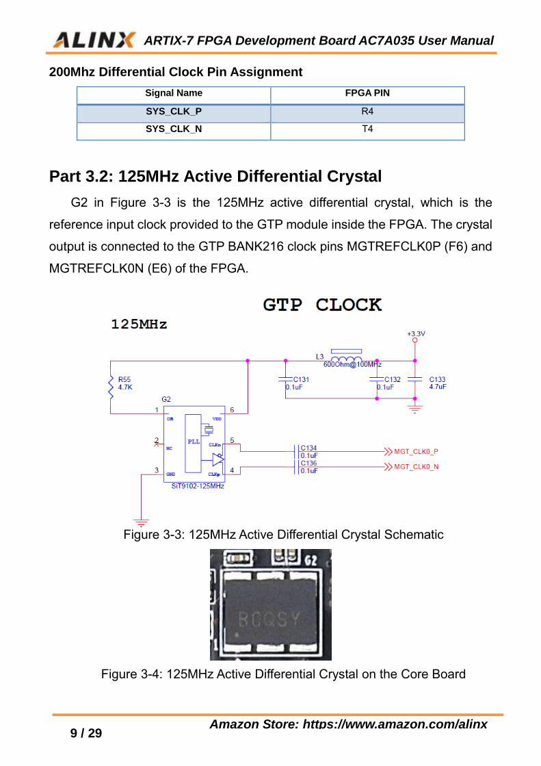
Figure 3-2: 200Mhz Active Differential Crystal on the Core Board
ARTIX-7 FPGA Development Board AC7A035 User Manual
9 / 29
Amazon Store: https://www.amazon.com/alinx
200Mhz Differential Clock Pin Assignment
Signal Name FPGA PIN
SYS_CLK_P R4
SYS_CLK_N T4
Part 3.2: 125MHz Active Differential Crystal
G2 in Figure 3-3 is the 125MHz active differential crystal, which is the
reference input clock provided to the GTP module inside the FPGA. The crystal
output is connected to the GTP BANK216 clock pins MGTREFCLK0P (F6) and
MGTREFCLK0N (E6) of the FPGA.
Figure 3-3: 125MHz Active Differential Crystal Schematic
Figure 3-4: 125MHz Active Differential Crystal on the Core Board
ARTIX-7 FPGA Development Board AC7A035 User Manual
10 / 29
Amazon Store: https://www.amazon.com/alinx
125MHz Differential Clock Pin Assignment
Net Name FPGA PIN
MGT_CLK0_P F6
MGT_CLK0_N E6
Part 4: DDR3 DRAM
The FPGA core board AC7A035 is equipped with two Micron 4Gbit
(512MB) DDR3 chips (8Gbit in totally), model is MT41J256M16HA-125
(compatible with MT41K256M16HA-125). The DDR3 SDRAM has a maximum
operating speed of 400MHz (data rate 800Mbps). The DDR3 memory system
is directly connected to the memory interface of the BANK 34 and BANK35 of
the FPGA. The specific configuration of DDR3 SDRAM is shown in Table 4-1.
Bit Number Chip Model Capacity Factory U5,U6 MT41J256M16HA-125 256M x 16bit Micron
Table 4-1: DDR3 SDRAM Configuration
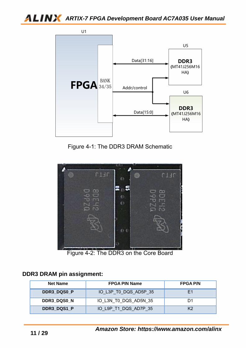
The hardware design of DDR3 requires strict consideration of signal
integrity. We have fully considered the matching resistor/terminal resistance,
trace impedance control, and trace length control in circuit design and PCB
design to ensure high-speed and stable operation of DDR3. Figure 4-1 details
the hardware connection of DDR3 DRAM
ARTIX-7 FPGA Development Board AC7A035 User Manual
11 / 29
Amazon Store: https://www.amazon.com/alinx
FPGA
DDR3(MT41J256M16
HA)
Data[31:16]
U5
U1
BANK34/35
DDR3(MT41J256M16
HA)
U6
Data[15:0]
Addr/control
Figure 4-1: The DDR3 DRAM Schematic
Figure 4-2: The DDR3 on the Core Board
DDR3 DRAM pin assignment:
Net Name FPGA PIN Name FPGA P/N
DDR3_DQS0_P IO_L3P_T0_DQS_AD5P_35 E1
DDR3_DQS0_N IO_L3N_T0_DQS_AD5N_35 D1
DDR3_DQS1_P IO_L9P_T1_DQS_AD7P_35 K2
ARTIX-7 FPGA Development Board AC7A035 User Manual
12 / 29
Amazon Store: https://www.amazon.com/alinx
DDR3_DQS1_N IO_L9N_T1_DQS_AD7N_35 J2
DDR3_DQS2_P IO_L15P_T2_DQS_35 M1
DDR3_DQS2_N IO_L15N_T2_DQS_35 L1
DDR3_DQS3_P IO_L21P_T3_DQS_35 P5
DDR3_DQS3_N IO_L21N_T3_DQS_35 P4
DDR3_DQ[0] IO_L2P_T0_AD12P_35 C2
DDR3_DQ [1] IO_L5P_T0_AD13P_35 G1
DDR3_DQ [2] IO_L1N_T0_AD4N_35 A1
DDR3_DQ [3] IO_L6P_T0_35 F3
DDR3_DQ [4] IO_L2N_T0_AD12N_35 B2
DDR3_DQ [5] IO_L5N_T0_AD13N_35 F1
DDR3_DQ [6] IO_L1P_T0_AD4P_35 B1
DDR3_DQ [7] IO_L4P_T0_35 E2
DDR3_DQ [8] IO_L11P_T1_SRCC_35 H3
DDR3_DQ [9] IO_L11N_T1_SRCC_35 G3
DDR3_DQ [10] IO_L8P_T1_AD14P_35 H2
DDR3_DQ [11] IO_L10N_T1_AD15N_35 H5
DDR3_DQ [12] IO_L7N_T1_AD6N_35 J1
DDR3_DQ [13] IO_L10P_T1_AD15P_35 J5
DDR3_DQ [14] IO_L7P_T1_AD6P_35 K1
DDR3_DQ [15] IO_L12P_T1_MRCC_35 H4
DDR3_DQ [16] IO_L18N_T2_35 L4
DDR3_DQ [17] IO_L16P_T2_35 M3
DDR3_DQ [18] IO_L14P_T2_SRCC_35 L3
DDR3_DQ [19] IO_L17N_T2_35 J6
DDR3_DQ [20] IO_L14N_T2_SRCC_35 K3
DDR3_DQ [21] IO_L17P_T2_35 K6
DDR3_DQ [22] IO_L13N_T2_MRCC_35 J4
DDR3_DQ [23] IO_L18P_T2_35 L5
DDR3_DQ [24] IO_L20N_T3_35 P1
DDR3_DQ [25] IO_L19P_T3_35 N4
DDR3_DQ [26] IO_L20P_T3_35 R1
DDR3_DQ [27] IO_L22N_T3_35 N2
DDR3_DQ [28] IO_L23P_T3_35 M6
DDR3_DQ [29] IO_L24N_T3_35 N5
DDR3_DQ [30] IO_L24P_T3_35 P6
ARTIX-7 FPGA Development Board AC7A035 User Manual
13 / 29
Amazon Store: https://www.amazon.com/alinx
DDR3_DQ [31] IO_L22P_T3_35 P2
DDR3_DM0 IO_L4N_T0_35 D2
DDR3_DM1 IO_L8N_T1_AD14N_35 G2
DDR3_DM2 IO_L16N_T2_35 M2
DDR3_DM3 IO_L23N_T3_35 M5
DDR3_A[0] IO_L11N_T1_SRCC_34 AA4
DDR3_A[1] IO_L8N_T1_34 AB2
DDR3_A[2] IO_L10P_T1_34 AA5
DDR3_A[3] IO_L10N_T1_34 AB5
DDR3_A[4] IO_L7N_T1_34 AB1
DDR3_A[5] IO_L6P_T0_34 U3
DDR3_A[6] IO_L5P_T0_34 W1
DDR3_A[7] IO_L1P_T0_34 T1
DDR3_A[8] IO_L2N_T0_34 V2
DDR3_A[9] IO_L2P_T0_34 U2
DDR3_A[10] IO_L5N_T0_34 Y1
DDR3_A[11] IO_L4P_T0_34 W2
DDR3_A[12] IO_L4N_T0_34 Y2
DDR3_A[13] IO_L1N_T0_34 U1
DDR3_A[14] IO_L6N_T0_VREF_34 V3
DDR3_BA[0] IO_L9N_T1_DQS_34 AA3
DDR3_BA[1] IO_L9P_T1_DQS_34 Y3
DDR3_BA[2] IO_L11P_T1_SRCC_34 Y4
DDR3_S0 IO_L8P_T1_34 AB3
DDR3_RAS IO_L12P_T1_MRCC_34 V4
DDR3_CAS IO_L12N_T1_MRCC_34 W4
DDR3_WE IO_L7P_T1_34 AA1
DDR3_ODT IO_L14N_T2_SRCC_34 U5
DDR3_RESET IO_L15P_T2_DQS_34 W6
DDR3_CLK_P IO_L3P_T0_DQS_34 R3
DDR3_CLK_N IO_L3N_T0_DQS_34 R2
DDR3_CKE IO_L14P_T2_SRCC_34 T5
Part 5: QSPI Flash
The FPGA core board AC7A035 is equipped with one 128Mbit QSPI

ARTIX-7 FPGA Development Board AC7A035 User Manual
14 / 29
Amazon Store: https://www.amazon.com/alinx
FLASH, and the model is N25Q128, which uses the 3.3V CMOS voltage
standard. Due to the non-volatile nature of QSPI FLASH, it can be used as a
boot device for the system to store the boot image of the system. These
images mainly include FPGA bit files, ARM application code, soft core
application code and other user data files. The specific models and related
parameters of SPI FLASH are shown in Table 5-1.
Position Model Capacity Factory
U8 N25Q128 128M Bit Numonyx
Table 5-1: QSPI FLASH Specification
QSPI FLASH is connected to the dedicated pins of BANK0 and BANK14 of
the FPGA chip. The clock pin is connected to CCLK0 of BANK0, and other data
and chip select signals are connected to D00~D03 and FCS pins of BANK14
respectively. Figure 5-1 shows the hardware connection of QSPI Flash.
Figure 5-1: QSPI Flash Schematic
ARTIX-7 FPGA Development Board AC7A035 User Manual
15 / 29
Amazon Store: https://www.amazon.com/alinx
QSPI Flash pin assignments:
Net Name FPGA PIN Name FPGA P/N
QSPI_CLK CCLK_0 L12
QSPI_CS IO_L6P_T0_FCS_B_14 T19
QSPI_DQ0 IO_L1P_T0_D00_MOSI_14 P22
QSPI_DQ1 IO_L1N_T0_D01_DIN_14 R22
QSPI_DQ2 IO_L2P_T0_D02_14 P21
QSPI_DQ3 IO_L2N_T0_D03_14 R21
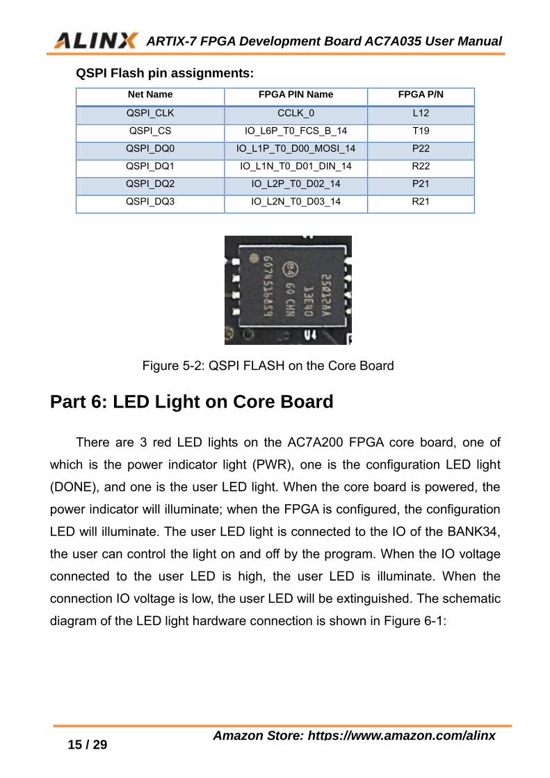
Figure 5-2: QSPI FLASH on the Core Board
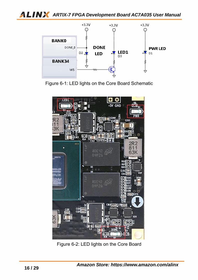
Part 6: LED Light on Core Board
There are 3 red LED lights on the AC7A200 FPGA core board, one of
which is the power indicator light (PWR), one is the configuration LED light
(DONE), and one is the user LED light. When the core board is powered, the
power indicator will illuminate; when the FPGA is configured, the configuration
LED will illuminate. The user LED light is connected to the IO of the BANK34,
the user can control the light on and off by the program. When the IO voltage
connected to the user LED is high, the user LED is illuminate. When the
connection IO voltage is low, the user LED will be extinguished. The schematic
diagram of the LED light hardware connection is shown in Figure 6-1:
ARTIX-7 FPGA Development Board AC7A035 User Manual
16 / 29
Amazon Store: https://www.amazon.com/alinx
Figure 6-1: LED lights on the Core Board Schematic
Figure 6-2: LED lights on the Core Board
ARTIX-7 FPGA Development Board AC7A035 User Manual
17 / 29
Amazon Store: https://www.amazon.com/alinx
User LEDs Pin Assignment
Part 7: JTAG Interface
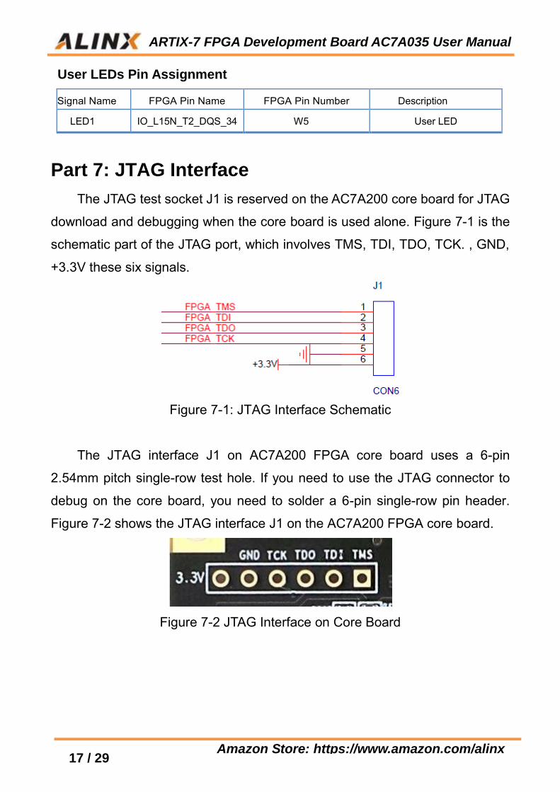
The JTAG test socket J1 is reserved on the AC7A200 core board for JTAG
download and debugging when the core board is used alone. Figure 7-1 is the
schematic part of the JTAG port, which involves TMS, TDI, TDO, TCK. , GND,
+3.3V these six signals.
Figure 7-1: JTAG Interface Schematic
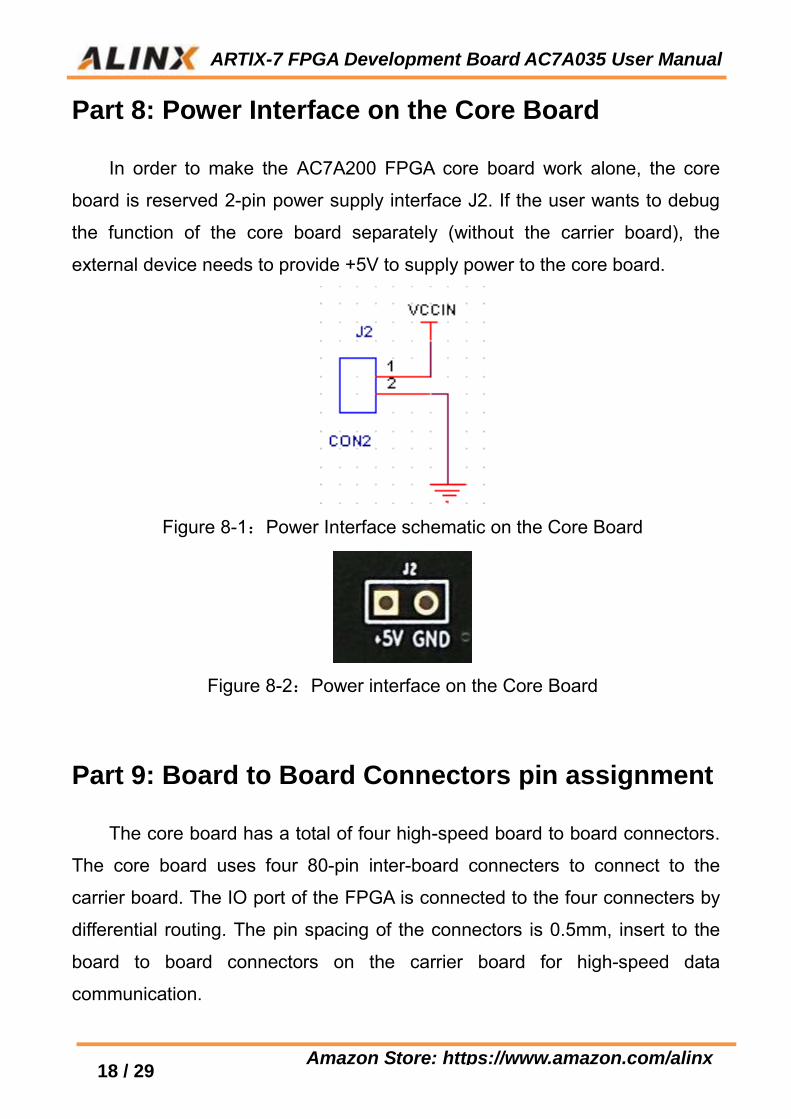
The JTAG interface J1 on AC7A200 FPGA core board uses a 6-pin
2.54mm pitch single-row test hole. If you need to use the JTAG connector to
debug on the core board, you need to solder a 6-pin single-row pin header.
Figure 7-2 shows the JTAG interface J1 on the AC7A200 FPGA core board.
Figure 7-2 JTAG Interface on Core Board
Signal Name FPGA Pin Name FPGA Pin Number Description
LED1 IO_L15N_T2_DQS_34 W5 User LED
ARTIX-7 FPGA Development Board AC7A035 User Manual
18 / 29
Amazon Store: https://www.amazon.com/alinx
Part 8: Power Interface on the Core Board
In order to make the AC7A200 FPGA core board work alone, the core
board is reserved 2-pin power supply interface J2. If the user wants to debug
the function of the core board separately (without the carrier board), the
external device needs to provide +5V to supply power to the core board.
Figure 8-1:Power Interface schematic on the Core Board
Figure 8-2:Power interface on the Core Board
Part 9: Board to Board Connectors pin assignment
The core board has a total of four high-speed board to board connectors.
The core board uses four 80-pin inter-board connecters to connect to the
carrier board. The IO port of the FPGA is connected to the four connecters by
differential routing. The pin spacing of the connectors is 0.5mm, insert to the
board to board connectors on the carrier board for high-speed data
communication.
ARTIX-7 FPGA Development Board AC7A035 User Manual
19 / 29
Amazon Store: https://www.amazon.com/alinx
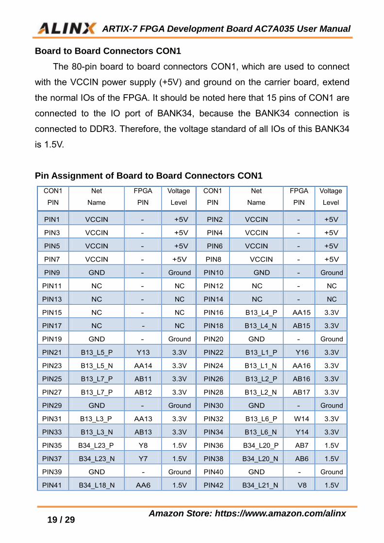
Board to Board Connectors CON1
The 80-pin board to board connectors CON1, which are used to connect
with the VCCIN power supply (+5V) and ground on the carrier board, extend
the normal IOs of the FPGA. It should be noted here that 15 pins of CON1 are
connected to the IO port of BANK34, because the BANK34 connection is
connected to DDR3. Therefore, the voltage standard of all IOs of this BANK34
is 1.5V.
Pin Assignment of Board to Board Connectors CON1
CON1
PIN
Net
Name
FPGA
PIN
Voltage
Level
CON1
PIN
Net
Name
FPGA
PIN
Voltage
Level
PIN1 VCCIN - +5V PIN2 VCCIN - +5V
PIN3 VCCIN - +5V PIN4 VCCIN - +5V
PIN5 VCCIN - +5V PIN6 VCCIN - +5V
PIN7 VCCIN - +5V PIN8 VCCIN - +5V
PIN9 GND - Ground PIN10 GND - Ground
PIN11 NC - NC PIN12 NC - NC
PIN13 NC - NC PIN14 NC - NC
PIN15 NC - NC PIN16 B13_L4_P AA15 3.3V
PIN17 NC - NC PIN18 B13_L4_N AB15 3.3V
PIN19 GND - Ground PIN20 GND - Ground
PIN21 B13_L5_P Y13 3.3V PIN22 B13_L1_P Y16 3.3V
PIN23 B13_L5_N AA14 3.3V PIN24 B13_L1_N AA16 3.3V
PIN25 B13_L7_P AB11 3.3V PIN26 B13_L2_P AB16 3.3V
PIN27 B13_L7_P AB12 3.3V PIN28 B13_L2_N AB17 3.3V
PIN29 GND - Ground PIN30 GND - Ground
PIN31 B13_L3_P AA13 3.3V PIN32 B13_L6_P W14 3.3V
PIN33 B13_L3_N AB13 3.3V PIN34 B13_L6_N Y14 3.3V
PIN35 B34_L23_P Y8 1.5V PIN36 B34_L20_P AB7 1.5V
PIN37 B34_L23_N Y7 1.5V PIN38 B34_L20_N AB6 1.5V
PIN39 GND - Ground PIN40 GND - Ground
PIN41 B34_L18_N AA6 1.5V PIN42 B34_L21_N V8 1.5V
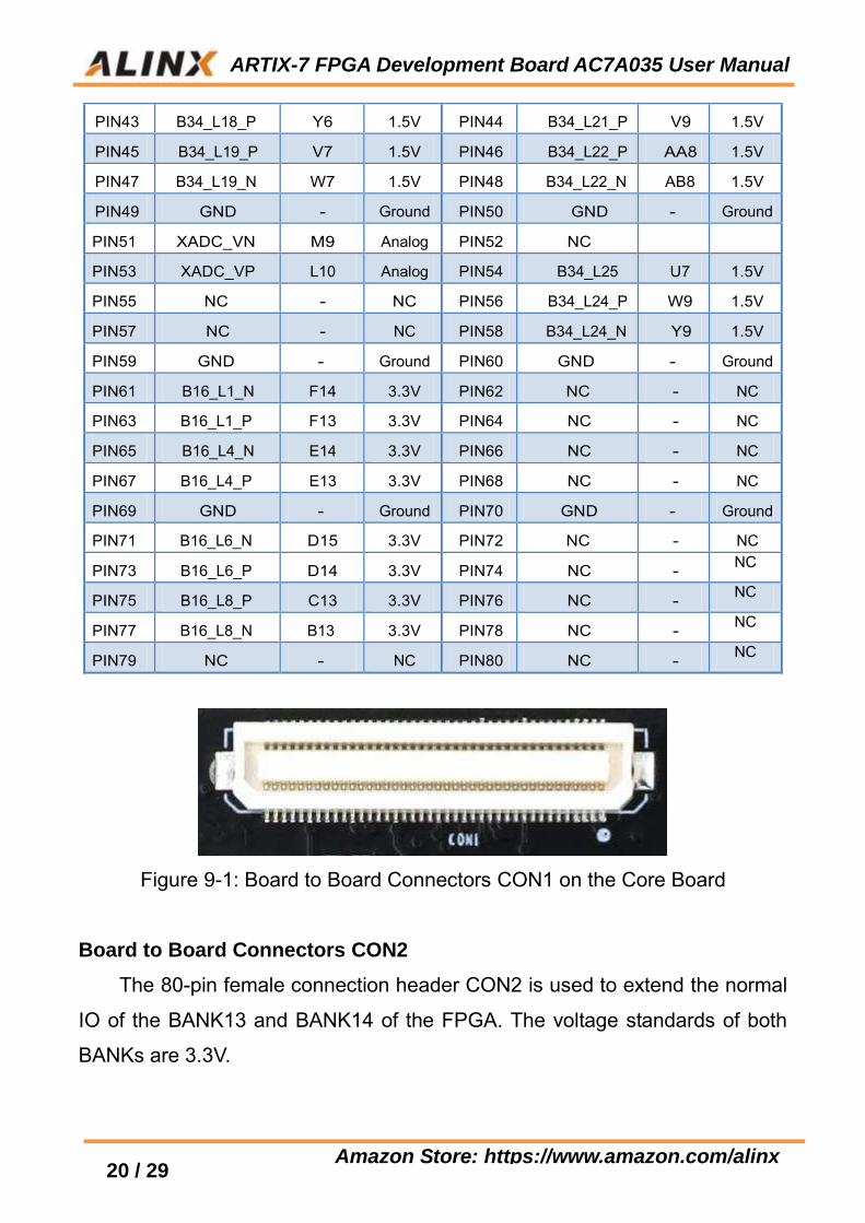
ARTIX-7 FPGA Development Board AC7A035 User Manual
20 / 29
Amazon Store: https://www.amazon.com/alinx
PIN43 B34_L18_P Y6 1.5V PIN44 B34_L21_P V9 1.5V
PIN45 B34_L19_P V7 1.5V PIN46 B34_L22_P AA8 1.5V
PIN47 B34_L19_N W7 1.5V PIN48 B34_L22_N AB8 1.5V
PIN49 GND - Ground PIN50 GND - Ground
PIN51 XADC_VN M9 Analog PIN52 NC
PIN53 XADC_VP L10 Analog PIN54 B34_L25 U7 1.5V
PIN55 NC - NC PIN56 B34_L24_P W9 1.5V
PIN57 NC - NC PIN58 B34_L24_N Y9 1.5V
PIN59 GND - Ground PIN60 GND - Ground
PIN61 B16_L1_N F14 3.3V PIN62 NC - NC
PIN63 B16_L1_P F13 3.3V PIN64 NC - NC
PIN65 B16_L4_N E14 3.3V PIN66 NC - NC
PIN67 B16_L4_P E13 3.3V PIN68 NC - NC
PIN69 GND - Ground PIN70 GND - Ground
PIN71 B16_L6_N D15 3.3V PIN72 NC - NC
PIN73 B16_L6_P D14 3.3V PIN74 NC - NC
PIN75 B16_L8_P C13 3.3V PIN76 NC - NC
PIN77 B16_L8_N B13 3.3V PIN78 NC - NC
PIN79 NC - NC PIN80 NC - NC
Figure 9-1: Board to Board Connectors CON1 on the Core Board
Board to Board Connectors CON2
The 80-pin female connection header CON2 is used to extend the normal
IO of the BANK13 and BANK14 of the FPGA. The voltage standards of both
BANKs are 3.3V.
ARTIX-7 FPGA Development Board AC7A035 User Manual
21 / 29
Amazon Store: https://www.amazon.com/alinx
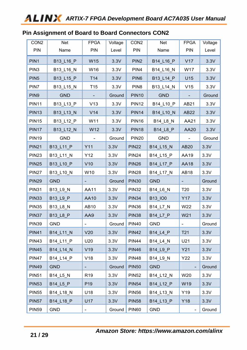
Pin Assignment of Board to Board Connectors CON2
CON2
PIN
Net
Name
FPGA
PIN
Voltage
Level
CON2
PIN
Net
Name
FPGA
PIN
Voltage
Level
PIN1 B13_L16_P W15 3.3V PIN2 B14_L16_P V17 3.3V
PIN3 B13_L16_N W16 3.3V PIN4 B14_L16_N W17 3.3V
PIN5 B13_L15_P T14 3.3V PIN6 B13_L14_P U15 3.3V
PIN7 B13_L15_N T15 3.3V PIN8 B13_L14_N V15 3.3V
PIN9 GND - Ground PIN10 GND - Ground
PIN11 B13_L13_P V13 3.3V PIN12 B14_L10_P AB21 3.3V
PIN13 B13_L13_N V14 3.3V PIN14 B14_L10_N AB22 3.3V
PIN15 B13_L12_P W11 3.3V PIN16 B14_L8_N AA21 3.3V
PIN17 B13_L12_N W12 3.3V PIN18 B14_L8_P AA20 3.3V
PIN19 GND - Ground PIN20 GND - Ground
PIN21 B13_L11_P Y11 3.3V PIN22 B14_L15_N AB20 3.3V
PIN23 B13_L11_N Y12 3.3V PIN24 B14_L15_P AA19 3.3V
PIN25 B13_L10_P V10 3.3V PIN26 B14_L17_P AA18 3.3V
PIN27 B13_L10_N W10 3.3V PIN28 B14_L17_N AB18 3.3V
PIN29 GND - Ground PIN30 GND - Ground
PIN31 B13_L9_N AA11 3.3V PIN32 B14_L6_N T20 3.3V
PIN33 B13_L9_P AA10 3.3V PIN34 B13_IO0 Y17 3.3V
PIN35 B13_L8_N AB10 3.3V PIN36 B14_L7_N W22 3.3V
PIN37 B13_L8_P AA9 3.3V PIN38 B14_L7_P W21 3.3V
PIN39 GND - Ground PIN40 GND - Ground
PIN41 B14_L11_N V20 3.3V PIN42 B14_L4_P T21 3.3V
PIN43 B14_L11_P U20 3.3V PIN44 B14_L4_N U21 3.3V
PIN45 B14_L14_N V19 3.3V PIN46 B14_L9_P Y21 3.3V
PIN47 B14_L14_P V18 3.3V PIN48 B14_L9_N Y22 3.3V
PIN49 GND - Ground PIN50 GND - Ground
PIN51 B14_L5_N R19 3.3V PIN52 B14_L12_N W20 3.3V
PIN53 B14_L5_P P19 3.3V PIN54 B14_L12_P W19 3.3V
PIN55 B14_L18_N U18 3.3V PIN56 B14_L13_N Y19 3.3V
PIN57 B14_L18_P U17 3.3V PIN58 B14_L13_P Y18 3.3V
PIN59 GND - Ground PIN60 GND - Ground
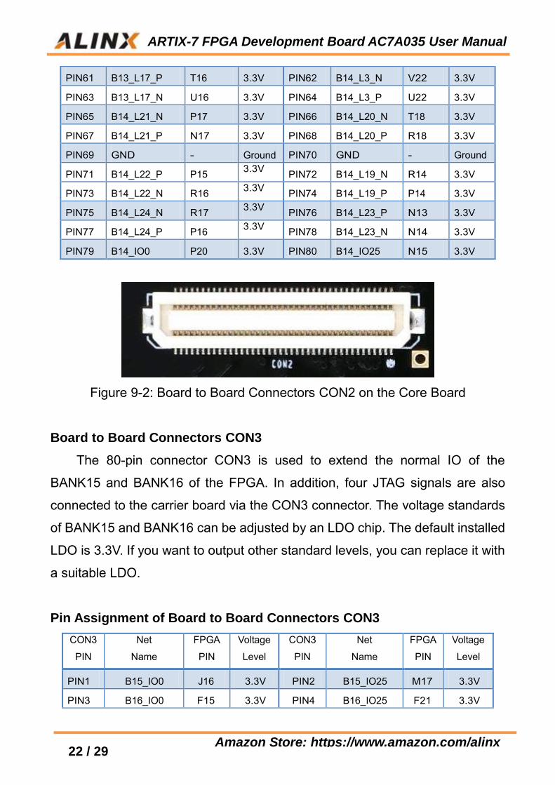
ARTIX-7 FPGA Development Board AC7A035 User Manual
22 / 29
Amazon Store: https://www.amazon.com/alinx
PIN61 B13_L17_P T16 3.3V PIN62 B14_L3_N V22 3.3V
PIN63 B13_L17_N U16 3.3V PIN64 B14_L3_P U22 3.3V
PIN65 B14_L21_N P17 3.3V PIN66 B14_L20_N T18 3.3V
PIN67 B14_L21_P N17 3.3V PIN68 B14_L20_P R18 3.3V
PIN69 GND - Ground PIN70 GND - Ground
PIN71 B14_L22_P P15 3.3V PIN72 B14_L19_N R14 3.3V
PIN73 B14_L22_N R16 3.3V PIN74 B14_L19_P P14 3.3V
PIN75 B14_L24_N R17 3.3V PIN76 B14_L23_P N13 3.3V
PIN77 B14_L24_P P16 3.3V PIN78 B14_L23_N N14 3.3V
PIN79 B14_IO0 P20 3.3V PIN80 B14_IO25 N15 3.3V
Figure 9-2: Board to Board Connectors CON2 on the Core Board
Board to Board Connectors CON3
The 80-pin connector CON3 is used to extend the normal IO of the
BANK15 and BANK16 of the FPGA. In addition, four JTAG signals are also
connected to the carrier board via the CON3 connector. The voltage standards
of BANK15 and BANK16 can be adjusted by an LDO chip. The default installed
LDO is 3.3V. If you want to output other standard levels, you can replace it with
a suitable LDO.
Pin Assignment of Board to Board Connectors CON3
CON3
PIN
Net
Name
FPGA
PIN
Voltage
Level
CON3
PIN
Net
Name
FPGA
PIN
Voltage
Level
PIN1 B15_IO0 J16 3.3V PIN2 B15_IO25 M17 3.3V
PIN3 B16_IO0 F15 3.3V PIN4 B16_IO25 F21 3.3V
ARTIX-7 FPGA Development Board AC7A035 User Manual
23 / 29
Amazon Store: https://www.amazon.com/alinx
PIN5 B15_L4_P G17 3.3V PIN6 B16_L21_N A21 3.3V
PIN7 B15_L4_N G18 3.3V PIN8 B16_L21_P B21 3.3V
PIN9 GND - Ground PIN10 GND - Ground
PIN11 B15_L2_P G15 3.3V PIN12 B16_L23_P E21 3.3V
PIN13 B15_L2_N G16 3.3V PIN14 B16_L23_N D21 3.3V
PIN15 B15_L12_P J19 3.3V PIN16 B16_L22_P E22 3.3V
PIN17 B15_L12_N H19 3.3V PIN18 B16_L22_N D22 3.3V
PIN19 GND - Ground PIN20 GND - Ground
PIN21 B15_L11_P J20 3.3V PIN22 B16_L24_P G21 3.3V
PIN23 B15_L11_N J21 3.3V PIN24 B16_L24_N G22 3.3V
PIN25 B15_L1_N G13 3.3V PIN26 B15_L8_N G20 3.3V
PIN27 B15_L1_P H13 3.3V PIN28 B15_L8_P H20 3.3V
PIN29 GND - Ground PIN30 GND - Ground
PIN31 B15_L5_P J15 3.3V PIN32 B15_L7_N H22 3.3V
PIN33 B15_L5_N H15 3.3V PIN34 B15_L7_P J22 3.3V
PIN35 B15_L3_N H14 3.3V PIN36 B15_L9_P K21 3.3V
PIN37 B15_L3_P J14 3.3V PIN38 B15_L9_N K22 3.3V
PIN39 GND - Ground PIN40 GND - Ground
PIN41 B15_L19_P K13 3.3V PIN42 B15_L15_N M22 3.3V
PIN43 B15_L19_N K14 3.3V PIN44 B15_L15_P N22 3.3V
PIN45 B15_L20_P M13 3.3V PIN46 B15_L6_N H18 3.3V
PIN47 B15_L20_N L13 3.3V PIN48 B15_L6_P H17 3.3V
PIN49 GND - Ground PIN50 GND - Ground
PIN51 B15_L14_P L19 3.3V PIN52 B15_L13_N K19 3.3V
PIN53 B15_L14_N L20 3.3V PIN54 B15_L13_P K18 3.3V
PIN55 B15_L21_P K17 3.3V PIN56 B15_L10_P M21 3.3V
PIN57 B15_L21_N J17 3.3V PIN58 B15_L10_N L21 3.3V
PIN59 GND - Ground PIN60 GND - Ground
PIN61 B15_L23_P L16 3.3V PIN62 B15_L18_P N20 3.3V
PIN63 B15_L23_N K16 3.3V PIN64 B15_L18_N M20 3.3V
PIN65 B15_L22_P L14 3.3V PIN66 B15_L17_N N19 3.3V
PIN67 B15_L22_N L15 3.3V PIN68 B15_L17_P N18 3.3V
PIN69 GND - Ground PIN70 GND - Ground
ARTIX-7 FPGA Development Board AC7A035 User Manual
24 / 29
Amazon Store: https://www.amazon.com/alinx
PIN71 B15_L24_P M15 3.3V PIN72 B15_L16_P M18 3.3V
PIN73 B15_L24_N M16 3.3V PIN74 B15_L16_N L18 3.3V
PIN75 NC - PIN76 NC -
PIN77 FPGA_TCK V12 3.3V PIN78 FPGA_TDI R13 3.3V
PIN79 FPGA_TDO U13 3.3V PIN80 FPGA_TMS T13 3.3V
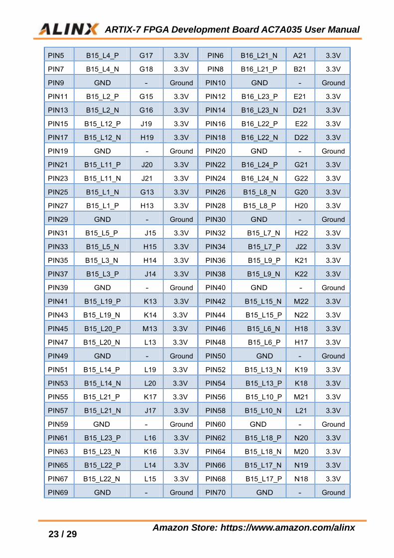
Figure 9-3: Board to Board Connectors CON3 on the Core Board
Board to Board Connectors CON4
The 80-Pin connector CON4 is used to extend the normal IO and GTP
high-speed data and clock signals of the FPGA BANK16. The voltage standard
of the IO port of BANK16 can be adjusted by an LDO chip. The default installed
LDO is 3.3V. If the user wants to output other standard levels, it can be
replaced by a suitable LDO. The high-speed data and clock signals of the GTP
are strictly differentially routed on the core board. The data lines are equal in
length and kept at a certain interval to prevent signal interference.
Pin Assignment of Board to Board Connectors CON4
CON4
PIN
Net
Name
FPGA
PIN
Voltage
Level
CON4
PIN
Net
Name
FPGA
PIN
Voltage
Level
PIN1 NC - - PIN2 - -
PIN3 NC - - PIN4 - -
PIN5 NC - - PIN6 - -
PIN7 NC - - PIN8 - -
PIN9 GND - Ground PIN10 GND - Ground

ARTIX-7 FPGA Development Board AC7A035 User Manual
25 / 29
Amazon Store: https://www.amazon.com/alinx
PIN11 NC - - PIN12 MGT_TX2_P B6 Diff
PIN13 NC - - PIN14 MGT_TX2_N A6 Diff
PIN15 GND - Ground PIN16 GND - Ground
PIN17 MGT_TX3_P D7 Diff PIN18 MGT_RX2_P B10 Diff
PIN19 MGT_TX3_N C7 Diff PIN20 MGT_RX2_N A10 Diff
PIN21 GND - Ground PIN22 GND - Ground
PIN23 MGT_RX3_P D9 Diff PIN24 MGT_TX0_P B4 Diff
PIN25 MGT_RX3_N C9 Diff PIN26 MGT_TX0_N A4 Diff
PIN27 GND - Ground PIN28 GND - Ground
PIN29 MGT_TX1_P D5 Diff PIN30 MGT_RX0_P B8 Diff
PIN31 MGT_TX1_N C5 Diff PIN32 MGT_RX0_N A8 Diff
PIN33 GND - Ground PIN34 GND - Ground
PIN35 MGT_RX1_P D11 Diff PIN36 MGT_CLK1_P F10 Diff
PIN37 MGT_RX1_N C11 Diff PIN38 MGT_CLK1_N E10 Diff
PIN39 GND - Ground PIN40 GND - Ground
PIN41 B16_L5_P E16 3.3V PIN42 B16_L2_P F16 3.3V
PIN43 B16_L5_N D16 3.3V PIN44 B16_L2_N E17 3.3V
PIN45 B16_L7_P B15 3.3V PIN46 B16_L3_P C14 3.3V
PIN47 B16_L7_N B16 3.3V PIN48 B16_L3_N C15 3.3V
PIN49 GND - Ground PIN50 GND - Ground
PIN51 B16_L9_P A15 3.3V PIN52 B16_L10_P A13 3.3V
PIN53 B16_L9_N A16 3.3V PIN54 B16_L10_N A14 3.3V
PIN55 B16_L11_P B17 3.3V PIN56 B16_L12_P D17 3.3V
PIN57 B16_L11_N B18 3.3V PIN58 B16_L12_N C17 3.3V
PIN59 GND - Ground PIN60 GND - Ground
PIN61 B16_L13_P C18 3.3V PIN62 B16_L14_P E19 3.3V
PIN63 B16_L13_N C19 3.3V PIN64 B16_L14_N D19 3.3V
PIN65 B16_L15_P F18 3.3V PIN66 B16_L16_P B20 3.3V
PIN67 B16_L15_N E18 3.3V PIN68 B16_L16_N A20 3.3V
PIN69 GND - Ground PIN70 GND - Ground
PIN71 B16_L17_P A18 3.3V PIN72 B16_L18_P F19 3.3V
PIN73 B16_L17_N A19 3.3V PIN74 B16_L18_N F20 3.3V
PIN75 B16_L19_P D20 3.3V PIN76 B16_L20_P C22 3.3V
PIN77 B16_L19_N C20 3.3V PIN78 B16_L20_N B22 3.3V
PIN79 NC - PIN80 NC -
ARTIX-7 FPGA Development Board AC7A035 User Manual
26 / 29
Amazon Store: https://www.amazon.com/alinx
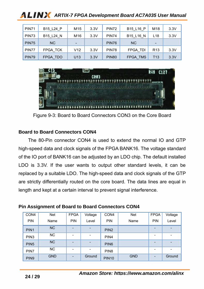
Figure 9-4: Board to Board Connectors CON4 on the Core Board
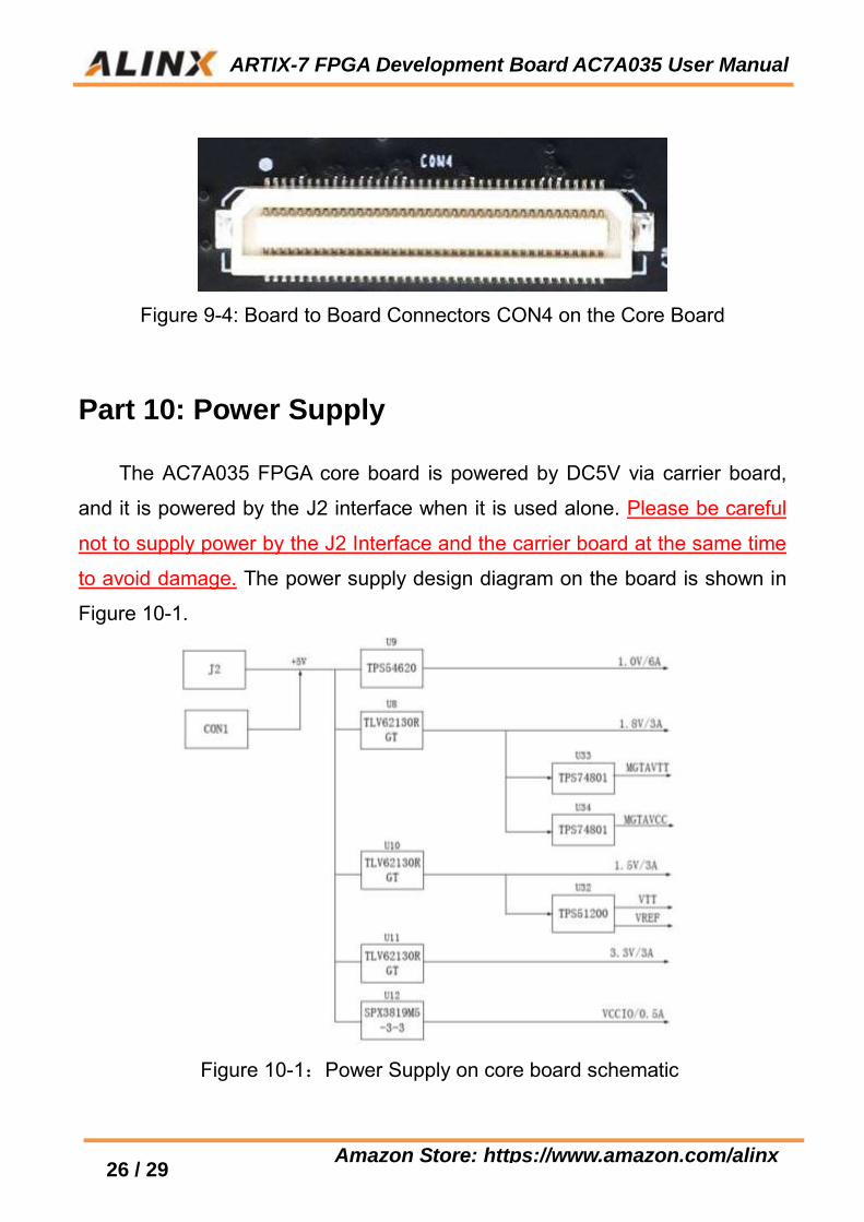
Part 10: Power Supply
The AC7A035 FPGA core board is powered by DC5V via carrier board,
and it is powered by the J2 interface when it is used alone. Please be careful
not to supply power by the J2 Interface and the carrier board at the same time
to avoid damage. The power supply design diagram on the board is shown in
Figure 10-1.
Figure 10-1:Power Supply on core board schematic
ARTIX-7 FPGA Development Board AC7A035 User Manual
27 / 29
Amazon Store: https://www.amazon.com/alinx
The core board is powered by +5V and converted to +3.3V, +1.5V, +1.8V,
+1.0V four-way power supply through three DC/DC power supply chip
TLV62130RGT. The current of +1.0V can be up to 6A, and the other three
output currents can be up to 3A. The VCCIO is generated by one
LDOSPX3819M5-3-3. VCCIO mainly supplies power to BANK15 and BANK16
of FPGA. Users can change the IO of BANK15,16 to different voltage
standards by replacing their LDO chip. The 1.5V generates the VTT and VREF
voltages required by DDR3 via TI's TPS51200. The 1.8V power supply of
MGTAVTT and MGTAVCC for the GTP transceiver is generated by TI's
TPS74801 chip. The functions of each power distribution are shown in the
following table: Power Supply Function
+1.0V FPGA Core Voltage
+1.8V FPGA auxiliary voltage, TPS74801 power supply
+3.3V VCCIO of Bank0,Bank13 and Bank14 of FPGA,QSIP FLASH, Clock Crystal
+1.5V DDR3, Bank34 and Bank35 of FPGA
VREF,VTT(+0.75V) DDR3
CCIP(+3.3V) FPGA Bank15, Bank16
MGTAVTT(+1.2V) GTP Transceiver Bank216 of FPGA
MGTVCC(+1.0V) GTP Transceiver Bank216 of FPGA
Because the power supply of Artix-7 FPGA has the power-on sequence
requirement, in the circuit design, we have designed according to the power
requirements of the chip, and the power-on is 1.0V->1.8V->(1.5 V, 3.3V, VCCIO)
and 1.0V-> MGTAVCC -> MGTAVTT, the circuit design to ensure the normal
operation of the chip.
The power circuit on the AC7A035 FPGA core board is shown in Figure
10-2:

ARTIX-7 FPGA Development Board AC7A035 User Manual
28 / 29
Amazon Store: https://www.amazon.com/alinx
Figure 10-2: Power Supply on the AC7A035 FPGA Core Board
ARTIX-7 FPGA Development Board AC7A035 User Manual
29 / 29
Amazon Store: https://www.amazon.com/alinx
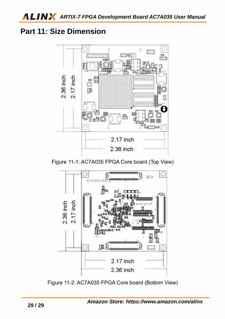
Part 11: Size Dimension
Figure 11-1: AC7A035 FPGA Core board (Top View)
Figure 11-2: AC7A035 FPGA Core board (Bottom View)