atmega control board manual v1 - cal polyusers.csc.calpoly.edu/~jseng/atmega_board.pdf · atmega...
TRANSCRIPT

ATMega Control Board Manual V1.0
Atmega Control Board.doc Page 1 / 32
ATMegaControl Board
Manual
V1.0
ATMega Control Board Manual V1.0
Atmega Control Board.doc Page 2 / 32
Chapter 1 - Introduction
1.1 Introduction
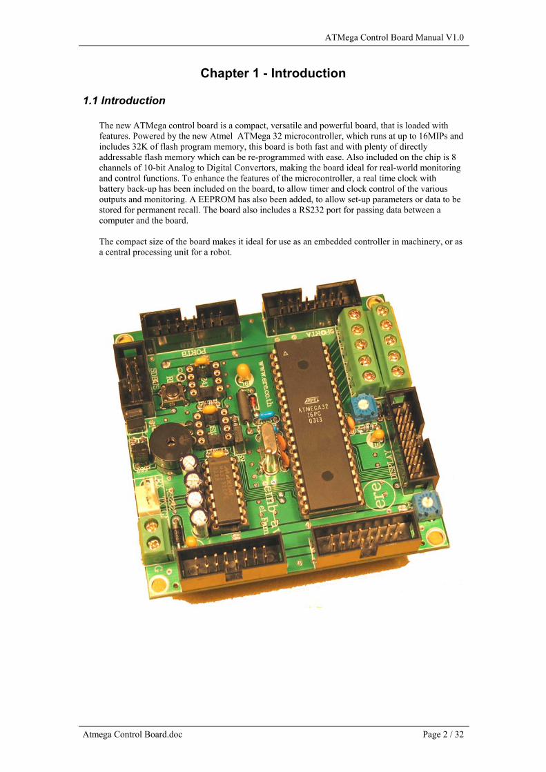
The new ATMega control board is a compact, versatile and powerful board, that is loaded withfeatures. Powered by the new Atmel ATMega 32 microcontroller, which runs at up to 16MIPs andincludes 32K of flash program memory, this board is both fast and with plenty of directlyaddressable flash memory which can be re-programmed with ease. Also included on the chip is 8channels of 10-bit Analog to Digital Convertors, making the board ideal for real-world monitoringand control functions. To enhance the features of the microcontroller, a real time clock withbattery back-up has been included on the board, to allow timer and clock control of the variousoutputs and monitoring. A EEPROM has also been added, to allow set-up parameters or data to bestored for permanent recall. The board also includes a RS232 port for passing data between acomputer and the board.
The compact size of the board makes it ideal for use as an embedded controller in machinery, or asa central processing unit for a robot.

ATMega Control Board Manual V1.0
Atmega Control Board.doc Page 3 / 32
1.2 Specifications of the ATMega Control Board
• Includes ATMega32 microcontroller, running at 16MHz• 32Kbytes of Flash Program Memory included within the microcontroller• All I/O pins connected to header terminals for easy connection and disconnection• 8 Channels of 10 bit Analog to Digital Convertors• LCD Connection and Contrast Trimpot included• Real Time Clock Socket with Battery Back-Up (DS1307 Option)• EEPROM Socket (24XX Option)• All necessary power supply components included• Reset Pushbutton on-board and pre-wired• Buzzer
1.3 Features of the Atmel ATMega 32 Microcontroller
• 32Kbytes Flash Program Memory• 2Kbyte Internal SRAM• 1024 Bytes EEPROM• 2 x 8-Bit Timer/Counters and 1 x 16-Bit Timer/Counter• Four PWM Channels• 8 Channel 10-Bit ADC• Programmable Serial USART• Master / Slave SPI Interface• Programmable Watchdog Timer• 32 Programmable I/O Lines• On-chip Analog Comparator• Six Sleep Modes for Current Consumption Minimization• Programmable Lock for Program Security

ATMega Control Board Manual V1.0
Atmega Control Board.doc Page 4 / 32
Chapter 2 – Program Download
2.1 Program Download – Computer and Board Setup
To prepare the board for programming, first place the board flat on the table near the computer.Follow the steps below and ensure the voltage source is a stable +5V supply to the board.
1. With the download unit as pictured below,
2. Connect the black 10-pin IDC Socket with the black 10 pin SDBus socket, located at the topleft of the board.
SDBUS

ATMega Control Board Manual V1.0
Atmega Control Board.doc Page 5 / 32
3. Now connect the grey DB25 connector to the printer port of the computer. As per the diagrambelow.
4. The next step is to connect a reliable and stable 5V supply to the ATMega Control Board.Ensure the polarity is correct as seen in the photo below,
5. With the supply connected the red LED on the download unit should illuminate. If this doesnot occur, recheck the supply for 5V.
6. The board is now ready for programming, run the download program provided on the CD. Formore information on the program, refer to the program section in this manual. Duringprogramming the yellow LED will illuminate.
+5V
0V / GND

ATMega Control Board Manual V1.0
Atmega Control Board.doc Page 6 / 32
7. After programming is complete the board will automatically commence running the program.
Precautions During Programming
1. The Port B pins PB5, PB6 and PB7 are used for downloading the program to the microcontroller.If these pins are currently connected to another circuit or external board, disconnect the wires oralternatively remove the IDCC connector from the Port B socket.
2. If there is a problem during programming, check there is adequate current supply available for theboard. During programming the current consumption can be quite high and the power supplyshould be capable of supplying this current. This can be checked, by monitoring the +5V voltageduring programming. If this dips substantially a larger power supply is required.
3. For the latest model computers, the speed may be too fast for the program to be accepted by themicrocontroller during download. Adjust the download speed by using the slider bar at the bottomof the programming software.
2.2 Installing and Running the Download Program
Prior to running the program, it will be necessary to run the setup program to install the software onyour computer. The program can be installed on any computer running Windows.
To run set-up, first insert the CD and open the program section of the CD. Double click on the set-upicon and the program will install automatically, follow the menus and when complete the program canbe run.
ATMega Control Board Manual V1.0
Atmega Control Board.doc Page 7 / 32
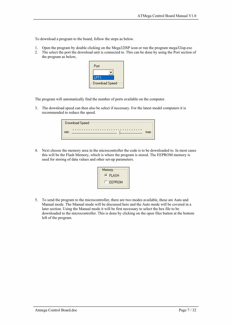
To download a program to the board, follow the steps as below.
1. Open the program by double clicking on the Mega32ISP icon or run the program mega32isp.exe2. The select the port the download unit is connected to. This can be done by using the Port section of
the program as below,
The program will automatically find the number of ports available on the computer.
3. The download speed can then also be select if necessary. For the latest model computers it isrecommended to reduce the speed.
4. Next choose the memory area in the microcontroller the code is to be downloaded to. In most casesthis will be the Flash Memory, which is where the program is stored. The EEPROM memory isused for storing of data values and other set-up parameters.
5. To send the program to the microcontroller, there are two modes available, these are Auto andManual mode. The Manual mode will be discussed here and the Auto mode will be covered in alater section. Using the Manual mode it will be first necessary to select the hex file to bedownloaded to the microcontroller. This is done by clicking on the open files button at the bottomleft of the program.

ATMega Control Board Manual V1.0
Atmega Control Board.doc Page 8 / 32
A file selection dialog box will then appear, for selecting the correct file.
Select the correct file and the file will then be loaded into the program buffer and appear in the buffersection of the program. Please note the hex file, needs to be pre-compiled and checked for errors, usingeither the AVR Studio program available from Atmel or another third party compiler.
6. Now erase the contents of the memory in the microcontroller, by clicking on the Chip Erase buttonunder the Manual section. As below,

ATMega Control Board Manual V1.0
Atmega Control Board.doc Page 9 / 32
The program memory can be checked, by using the Blank button to confirm it has been cleared.
6. The microcontroller is now ready for programming. Click on the Program button, and the yellowled on the download unit should come on while the program is being written to the ATMegaController Board. The Progress bar at the bottom left of the program, will also indicate the statusof the download.
7. When the message programming complete appears. The contents of the microcontroller memorycan be checked against the buffer, by using the Verify button. This will confirm the program hasbeen written correctly to the microcontroller. The program will now run automatically on theATMega board.
2.3 Other Features of the Program Software
Auto Mode: Auto mode is useful when the same program has to be written many times to a controlboard or a number of control boards. In the case of a factory using a number of these controllers, thiscould be used to program the complete set of boards.
To start with Auto Mode, first select settings as below,
A dialog box will then appear, giving the options for the instructions for the programmer to carry out.
Erase ProgramMemory

ATMega Control Board Manual V1.0
Atmega Control Board.doc Page 10 / 32
Typically, this would be Open File, Erase, Blank, Program, VerifyThe programmer will then automatically carry out these steps in sequence and halt if there is anyproblem. This is quite useful, if you are editing code for a particular application. The code can becorrected compiled and then press start will download the code automatically to the control board.
Security: It is recommended to study the section in the ATMega Datasheet regarding the use of theselock bits. As incorrect programming or setting will make further programming of the microcontrollerimpossible.
Firstly to obtain information on the status of the lock bits, a Read can be implemented to read thecurrent values. By pressing on the Info/Settings button, the status will then appear.
To set various lock bits, select the options required and then press okay. If you do not want to programthe values, press cancel.
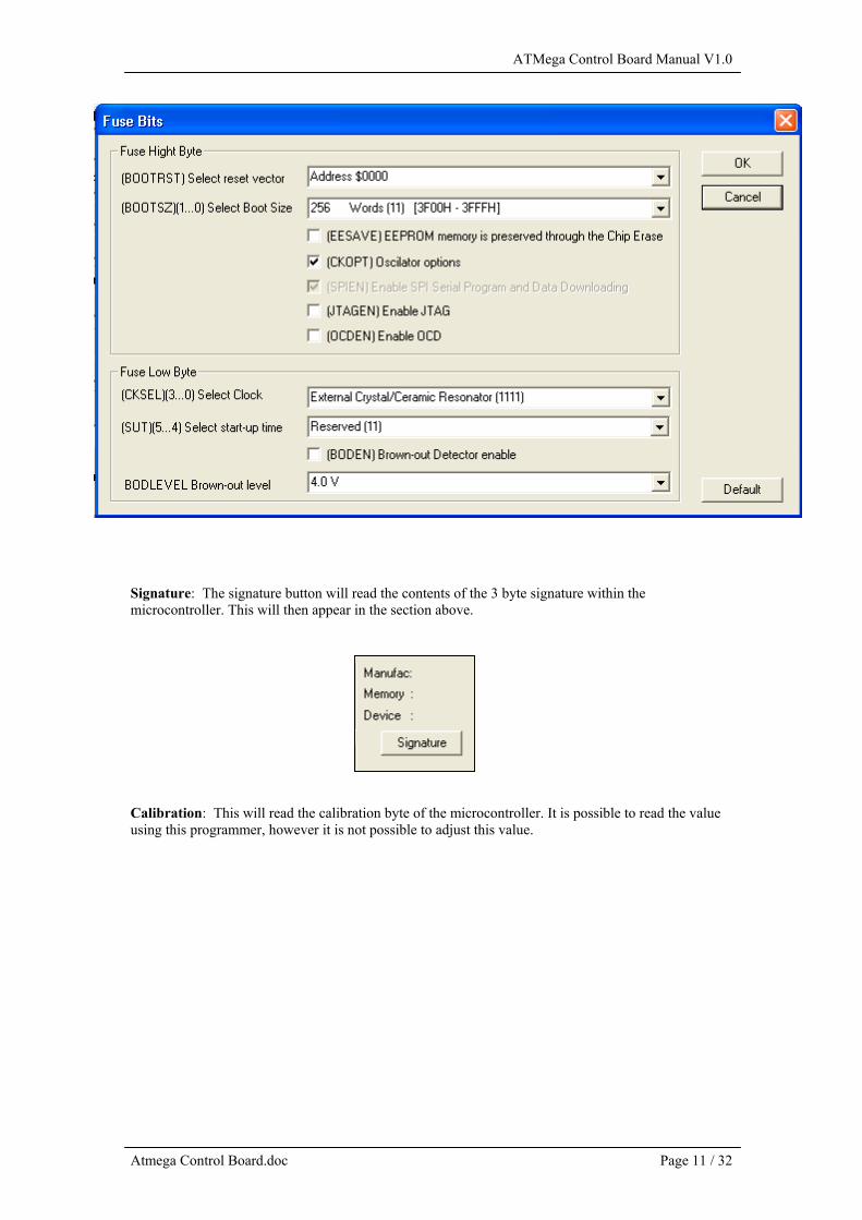
Fuse Bits: Similarly it is recommended to read the section in the ATMega manual regarding these fusebits. As changes in settings will result may affect the operation and ability to program the controlboard.
Basically these fuse bits, control the size and starting address for the bootloader section. They alsocontrol the oscillator options and start-up time. By clicking Okay will set the fuse bits, clicking cancelwill close the dialog box without programming the bits.
ATMega Control Board Manual V1.0
Atmega Control Board.doc Page 11 / 32
Signature: The signature button will read the contents of the 3 byte signature within themicrocontroller. This will then appear in the section above.
Calibration: This will read the calibration byte of the microcontroller. It is possible to read the valueusing this programmer, however it is not possible to adjust this value.

ATMega Control Board Manual V1.0
Atmega Control Board.doc Page 12 / 32
Chapter 3 – Board Reset
3.1 Using and Operation of Board Reset
The ATMega Control Board includes an on-board reset pushbutton. This will generate a reset of themicrocontroller, causing the microcontroller to restart the program sequence at the reset vector. All I/Oregisters are also reset to their initial values. After the reset is pressed and released, a shortdelay/timeout will occur to enable to voltages to stabilise.
3.2 Using the on-chip Brown-out Detection
The on-chip Brownout Detection is used to prevent the microcontroller from operating when thevoltage is low or not adequate. The brownout voltage setting can be adjusted by using the fuseBODLEVEL within the microcontroller. This can be set at either 2.7V or 4.0V, hysteresis is alsoincluded to prevent the microcontroller entering a race condition. After the voltage reaches thehysteresis level, a small time-out is included to ensure the voltage is stable. To enable BrownoutDetection the internal fuse BODEN needs to be enabled. This can be done during programming of theATMega.
ATMega Control Board Manual V1.0
Atmega Control Board.doc Page 13 / 32
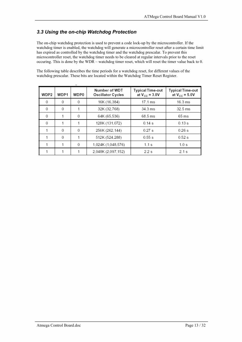
3.3 Using the on-chip Watchdog Protection
The on-chip watchdog protection is used to prevent a code lock-up by the microcontroller. If thewatchdog timer is enabled, the watchdog will generate a microcontroller reset after a certain time limithas expired as controlled by the watchdog timer and the watchdog prescalar. To prevent thismicrocontroller reset, the watchdog timer needs to be cleared at regular intervals prior to the resetoccuring. This is done by the WDR – watchdog timer reset, which will reset the timer value back to 0.
The following table describes the time periods for a watchdog reset, for different values of thewatchdog prescalar. These bits are located within the Watchdog Timer Reset Register.
ATMega Control Board Manual V1.0
Atmega Control Board.doc Page 14 / 32
Chapter 4 – Microcontroller Memory
4.1 Introduction
The ATMega memory consists of three parts. This is the data memory of SRAM which is used fortemporary storage of data values. Secondly the program memory, which is a Flash Memory, that can berewritten up to 10,000 times. Finally the EEPROM memory, which is used for permanent storage ofdata values or initial parameters for the microcontroller.
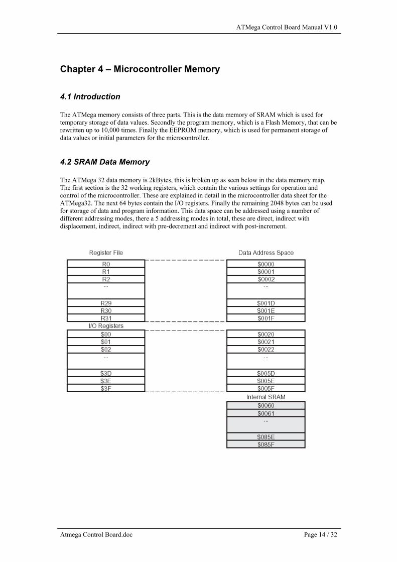
4.2 SRAM Data Memory
The ATMega 32 data memory is 2kBytes, this is broken up as seen below in the data memory map.The first section is the 32 working registers, which contain the various settings for operation andcontrol of the microcontroller. These are explained in detail in the microcontroller data sheet for theATMega32. The next 64 bytes contain the I/O registers. Finally the remaining 2048 bytes can be usedfor storage of data and program information. This data space can be addressed using a number ofdifferent addressing modes, there a 5 addressing modes in total, these are direct, indirect withdisplacement, indirect, indirect with pre-decrement and indirect with post-increment.

ATMega Control Board Manual V1.0
Atmega Control Board.doc Page 15 / 32
4.2 EEPROM Data Memory
The ATMega32 contains 1kByte of EEPROM memory. The memory can be written and rewritten up to100,000 times. The writing to and reading from this memory area is controlled by a number ofregisters. These are the EEPROM Address Register, EEPROM Data Register and EEPROM controlregister. By placing an address in the address register and then some data in the data register, followedby a write setting of the control register. The data value will then be written to the eeprom memory.Similarly for a eeprom read, by placing the desired address value in the eeprom address register andthen setting a eeprom read in the control register, a data byte will be read from the eeprom and placedin the eeprom data register. There are a number of timing contraints to this operation and some samplecode is provided in the ATMega data sheet and also on the CD-ROM.
4.4 Flash Program Memory
The ATMega32 contains 32kBytes of program flash memory. The ability to write and rewrite to thismemory easily, is what makes Flash Memory so popular. This memory is organized as 16k x 16 bits.The reason for this is that all AVR instructions are either 16 or 32 bits, thus 1 word comprises one 16bit instruction. The Atmega program counter is 14 bits wide, so the entire 16K memory space can beaddressed directly, with no need for setting of page bits, etc.
The arrangement of the program memory can be seen below. The boot flash section, is for the bootloader program, which can be used to program the flash memory by using the on-board UART on themicrocontroller. This is explained in more detail in the various Atmel ATMega data sheets.

ATMega Control Board Manual V1.0
Atmega Control Board.doc Page 16 / 32
Chapter 5 – Microcontroller Ports
5.1 Introduction
The ATMega32 has 4 ports, these are defined as PORTA, PORTB, PORTC and PORTD. Each of theport pins can be used for simple I/O, and in some cases contain a dual function for a peripheral functionwithin the micrcontroller. The location of each of the ports on the microcontroller is seen below. Theauxiliary function of the pin is also shown in the brackets. The control of the pins for either input oroutput is controlled by a series of registers, namely the data direction registers. To use the auxiliaryfunction of the various pins, this can be done by setting of the various control registers for thesefunctions.
5.2 Port A
The Port A can be used as I/O pins or as an ADC unit. In this section we will describe the operation forI/O, in a later chapter the ADC function will be discussed. The output of the microcontroller port A iswired directly to the port A socket on the control board. The PORTA socket is located at the top rightof the board. The pin configuration is shown in the diagram below from the top view.

ATMega Control Board Manual V1.0
Atmega Control Board.doc Page 17 / 32
When using port A for I/O the port pins can be set in either of 3 states, input, output and tri-state. Eachbit can also be set and operated independently of the other bits. When the port pin is set as an output,by using the port control register, a value of 1 at the data register, will set up the port to source current,setting the value to zero will allow the port pin to sink current. In the case of Port A, the total currentthe port can source is 200mA, thus it is possible to drive an LED directly, however care must beexercised to ensure the total port load is within this parameter.
When connecting the port pins to external circuits a ground connection should also be made to ensurethe signal is clear and has a common ground reference point. For this reason numerous ground pinshave been provided on the port A socket to allow a ground path with the port pin signal.
5.2 Port B
Port B can be used for general I/O or for a series of alternate functions. The alternate functions arelisted as below,
The pins PB5, PB6 and PB7 are related to the SPI function. The PB7-SCK provides the clock signal forreceiving or sending the data, using either the input/output to PB6-PB5. PB4 provides a further optionas a select function.
PB3 and PB2 provide an analog comparator, to monitor an analog input and provide an alarm should itreach or fall below a certain value.
PB1 and PB0 are used for counting input or as a signal to the timer.
The layout of the port B connection is seen below.
ATMega Control Board Manual V1.0
Atmega Control Board.doc Page 18 / 32
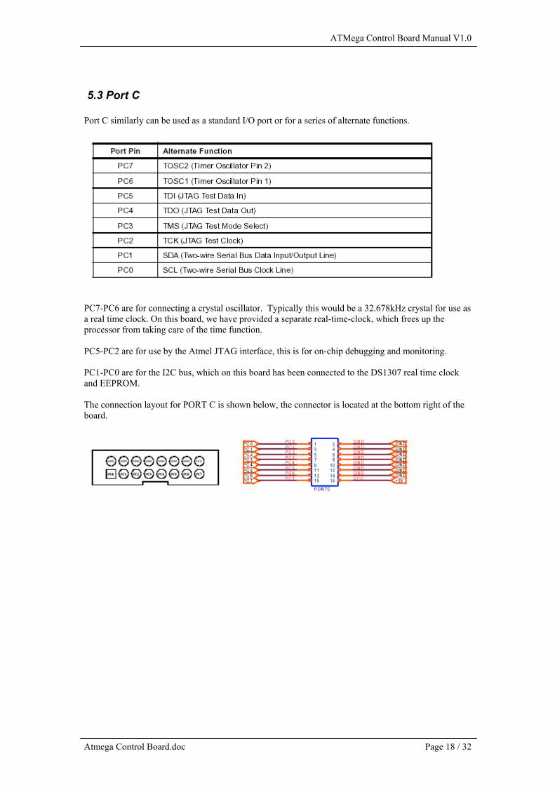
5.3 Port C
Port C similarly can be used as a standard I/O port or for a series of alternate functions.
PC7-PC6 are for connecting a crystal oscillator. Typically this would be a 32.678kHz crystal for use asa real time clock. On this board, we have provided a separate real-time-clock, which frees up theprocessor from taking care of the time function.
PC5-PC2 are for use by the Atmel JTAG interface, this is for on-chip debugging and monitoring.
PC1-PC0 are for the I2C bus, which on this board has been connected to the DS1307 real time clockand EEPROM.
The connection layout for PORT C is shown below, the connector is located at the bottom right of theboard.

ATMega Control Board Manual V1.0
Atmega Control Board.doc Page 19 / 32
5.3 Port D
The alternate functions for Port D are shown below, these are for the external interrupts, UART andTimer/Counter function.
PD7 – PD4 are used mainly for the PWM function within the ATMega. They can be also configured asan output signal for the timer counters.
PD3 – PD2 are for the external interrupts, to generate an interrupt within the microcontroller to jump toa certain program sequence.
PD1 – PD0 are the input output for the USART. These are also connected to the MAX232 on thecontrol board, to be able to connect to a computer for sending and receiving of messages via thecomputer parallel port.
Port D pin connection is shown below, also refer to the circuit diagram for the arrangement of theconnection to the USART.

ATMega Control Board Manual V1.0
Atmega Control Board.doc Page 20 / 32
Chapter 6 – I2C Bus
6.1 Introduction
The 2-wire or I2C bus, is ideal for connecting a number of devices/IC’s to a single data bus. Eachdevice has a unique address, and conversation is carried out between the device and the microcontrollerby specifying this address. Up to 128 devices can be connected using this bus. One wire of the bus isused as the clock and the other wire as the data line. Data can be sent and received using the single datawire, one device only though can act as the master which controls the process of data interchangebetween itself and the slave devices attached. A typical bus configuration can be seen below.Two pull-up resistors are required on each bus, to bring the bus voltage up to a constant 5V when idle.For more information regarding the format and protocol for message transfer, please refer to theATMega manual.
6.2 DS1307 Real Time Clock
The DS1307 Real Time Clock IC from Dallas Semiconductor, offers a number of features, that make ita useful real time clock in most systems. This is one of the most commonly used real-time clocks in usetoday in embedded applications. The time is maintained in a series of registers, that can be written to orread, by using the 2 wire serial connection. Also included is 56 bytes of scratchpad RAM, which can beused for temporary storage of values.

ATMega Control Board Manual V1.0
Atmega Control Board.doc Page 21 / 32
The register map and bit definitions are show in the following diagrams.
To send and receive data from the DS1307. It is necessary to send data in a certain format. This isnormally, in this order. Firstly the DS1307 address, which is ‘1101000’ for all DS1307’s. This isfollowed by the read/write bit, which is a 1 for a read and a 0 for a write.
Now for a register write, the address of the register to be written to will then be sent in a standard byte,following this the data to be written is transmitted, this can be a single byte or a series of bytes. To haltthe transmission, a stop condition is generated. This is explained in much more detail in the DS1307data sheet.
For a register read, the DS107 will start transmitting the data from the last register accessed. Thus, ifyou want to read a specific register, it is first necessary to carry out a register write, specifying thetarget address, and then switching to a register read to receive the required data.
Sample code for this is provided on the enclosed CD-ROM.

ATMega Control Board Manual V1.0
Atmega Control Board.doc Page 22 / 32
6.2 24LCXX EEPROM
The 24 series of eeproms, are ideal as a temporary storage device, which is maintained, even after thepower is disconnected. These can be used to store reading data, or parameters for the control board.
Writing and reading to these devices is similar to the DS1307 as described above. The address of thesedevices is ‘1010’ followed by the chip select bits A2, A1 and A0. These are set by using the three pinsof the eeprom A2, A1 and A0, which are normally at pin 1,2 and 3. Setting these pins to +5V, sets a 1and tying them to ground sets a 0. This is then followed by the read/write bit, as in the DS1307.The diagram below shows the format of this message.
To read and write to this device, there are a number of options. It is possible to do multi-byte reads andwrites to the device, however this has to be done using a standard format.
To do a single byte write, the following format is applicable. Firstly the control byte, with a byte write0 at the end. Followed by the address of the byte to write to, the length of this address depends on thesize of the device we are writing to. In the case below, we are writing to a 24LC128, which requires 14bits to specify the complete address. Finally the data byte and the stop bit to signify the transmission iscomplete.
For a Page write, which is a total of 64 bytes, the format is similar, with the exception that 64 bytes,follow the address bytes. The address register is automatically incremented for each byte. If more than64 bytes are sent, the counter will roll-over and rewrite the starting address locations.

ATMega Control Board Manual V1.0
Atmega Control Board.doc Page 23 / 32
For page reads, the format is similar and there are a number of options available, these are an addressread, a random byte read and a sequential byte read.
For an address read, only the control byte needs to be set, while specify a 1 at the R/W bit to indicate aread operation.
For a random read, this is again similar to the DS1307, where the address is first written to the deviceand then a read is specified to obtain the data value at that particular address.
For a sequential read, the process is identical to a random read, however a stop bit is not generated atthe completion of the first byte, it is instead initiated at the completion of the required read. If theaddress register reaches the limit, it will then rollover automatically to 0.

ATMega Control Board Manual V1.0
Atmega Control Board.doc Page 24 / 32
Chapter 7 – ADC
7.1 Introduction
Within the ATMega32 is a 10-bit successive approximation ADC. This is then connected to an 8-channel multiplexer, which will allow 8 single ended analog inputs to be connected to the ADC. Theseare connected to PORTA of the microcontroller, thus it will be necessary during set-up of themicrocontroller to specify which pins are to be used as ADC pins and which pins are for I/O.
The conversion time for the reading of the input is between 65 – 260 µs. It is important to allowadequate time for this conversion to take place, otherwise the read value from the ADC register will beincorrect. This is demonstrated in the sample code provided on the CD-ROM.
7.2 Voltage Reference
For the voltage reference this can be from either of 2 sources: internal or external. Internally there are 2voltage levels to choose from with 2.56V and AVCC, the voltage at pin 30 of the microcontroller. Thevoltage at AVCC is typically identical to Vcc, and Atmel recommend this voltage is within 0.3V ofVcc. Voltage input at the ADC pins of an identical value to the voltage reference, will result in a fullscale reading of 3FFh.
For an external voltage reference, this voltage is connected to the AREF pin 32 of the microcontroller.On the ATMega Development board, VR is provided to adjust this reference voltage. The voltage canbe adjusted between 0 – 5V, it is also important the input voltage to the ADC pins, does not exceed thisreference voltage. If this external reference is not required, it should be set to full range of +5V.
VR
Analog Inputs

ATMega Control Board Manual V1.0
Atmega Control Board.doc Page 25 / 32
7.2 Connecting to the ADC Terminals
For the analog inputs, these should be connected to the green pcb terminals, as an analog ground isprovided at the terminals. It is preferable not to use the PORTA digital terminals for the ADCconnection, as a separate ground is provided here for the digital signals, as it is good design practice toseparate the digital and analog ground, to prevent noise and incorrect readings.
7.3 Performing an A/D Conversion
The ADC is enabled by setting the ADC enable bit, ADEN which is located in the ADCSRA register.The voltage reference and input channel selections will not go into effect until this ADEN bit is set.Once the conversion is complete the result is placed in the 2 ADC data registers, ADCH for the highbyte and ADCL for the lower byte. The result is normally right adjusted, this can however be changedto be left adjusted by setting the ADLAR bit in ADMUX. The ADC also has its own interrupt whichshould be used to check the conversion is complete prior to reading these registers. A typical singlechannel conversion timing diagram is shown below.

ATMega Control Board Manual V1.0
Atmega Control Board.doc Page 26 / 32
Chapter 8 – LCD
8.1 Introduction
Provided on the ATMega Control Board is an easy to connect header for standard character LCD’s.This is ideal for display of real time data and also to give visual indication to the user. Also provided isa contrast trimpot for adjusting the contrast at pin 3 of standard LCD’s. Most 16x1, 16x2, 16x4, 20x2,20x4 and 40x2 Character LCD’s can connect to this port. Also provided is +5V at pin 16 for LCDbacklight, if this is included on the LCD.
8.2 Operation of the LCD
The connection provided is designed for the LCD to work in 4-bit mode. This is where only 4 lines ofdata are used, and a standard byte is split into 2, to send data to the LCD. This reduces the number ofmicrocontroller pins required to drive the LCD. Pins D4-D7 of the LCD are used for the data and pinsD3-D0 are grounded, the data pins are connected directly to PORTC pins PC4-PC7. Two additionalcontrol signals are required to clock the data into the LCD, these are the RS and E pins, these areconnected to PORTC pins PC2 and PC3 respectively. A third control connection from the LCD, R/W isgrounded, as it will only be necessary to write to the LCD and reads from the LCD are not required.
For the LCD backlight, pin 15 should be connected to the GND/BL- and pin 16 to the BL+ LCDconnection. A current limiting resistor is also included in the circuit to limit the current to the LEDbacklight. The value of this can be changed to increase the brightness of the backlight.
Sample code for a LCD is also provided on the accompanying CD-ROM.
8.2 Connection of the LCD
The connection to the LCD is quite straightforward. There are basically two types of terminalarrangements for LCD’s. These are where the connections are on either end of the board and aregrouped in 2 rows of 8. For this type of connection, it is easier to use a standard IDC socket to solderinto this LCD and then use a standard ribbon cable with IDC connectors on both ends, to connectbetween the board and the LCD. A diagram for this type of LCD is seen below.

ATMega Control Board Manual V1.0
Atmega Control Board.doc Page 27 / 32
For a type 1 LCD, this is where the LCD connections are located on the top or bottom of the LCD. Inthis case it will be necessary to use a standard IDC connector with ribbon cable for connection to theBoard. Then for the connection to the LCD, it will be necessary to swap each of the wires, as seen inthe diagram below. In this case we are swapping the 2nd wire on the ribbon cable and wiring it to thefirst LCD terminal. The first wire on the ribbon cable then goes terminal number 2 on the LCD. Careshould be taken to ensure the orientation of the IDC socket is correct, as it can be quite difficult torewire all the LCD if the connections are at the wrong end. Double check the wiring after this iscomplete, and damage can result if the +5V and gnd connections are incorrect.

ATMega Control Board Manual V1.0
Atmega Control Board.doc Page 28 / 32
Following completion of the wiring to the LCD, connect the IDC socket to the display socket as seen inthe picture below.
Contrast Adjustment
LCD Connector

ATMega Control Board Manual V1.0
Atmega Control Board.doc Page 29 / 32
Chapter 9 – RS232
9.1 Introduction
Provided within the ATMega32 is a USART, which can be used to connect your board to a standardRS232 port, either on a computer or another device. With this connection it is possible to pass databetween the board and a computer. The computer can for example, send commands to the board,receive data from the board for display in a Visual Basic or Delphi program etc.
9.2 Connecting to the RS232 Port
As standard RS232 signals are +15V, these signals cannot be connected directly to the microcontroller.Thus the MAX232 has been included in the circuit to provide an interface, to convert the +5Vmicrocontroller signals to the required RS232 standard. The MAX232 can be seen in the picture below.
A standard RS232 cable can be connected to the RS232 connector, by using a 3 pin polarized headerfor connection to the board. The RX and TX connections need to be swapped in this connection. Thiscan be seen in the diagram below. It may be necessary to check this with a multimeter, to ensure it iscorrect prior to connecting to the computer.
MAX232 Interface IC
RS232 Connector

ATMega Control Board Manual V1.0
Atmega Control Board.doc Page 30 / 32
9.2 Computer Programs and other Options
Firstly it is possible to connect to the board using a standard terminal program such as Hyperterminalor others. This program will send a handshake signal and initiate a basic communication check.
For Visual Basic, it is necessary to use the communication drivers, which are normally included withVB. These are the MSCOMM tools, that can be included in your program. Once these have been addedto the program, it is necessary to set the communication speed, parity etc. These values need to beidentical in both the microcontroller and the computer. The values are set in the microcontroller, bysetting the various USART control registers. It is important to read the USART section in the Atmegamanual, prior to proceeding, as a good understanding of this is required prior to proceeding.

ATMega Control Board Manual V1.0
Atmega Control Board.doc Page 31 / 32
Chapter 10 – Buzzer
10.1 Introduction
The buzzer is provided to give an audio indication of an alarm condition. By switching at differentfrequencies or lengthening and shortening the ON period, different warnings can be given. For examplea short chirp, can be used as a warning indication, while long ON periods can be used as an alarm.
10.2 Using The Buzzer
Using the buzzer is quite simple, just turn on (set bit to 1) port PD4 and the buzzer will sound. Settingthe PD4 bit back to zero will turn off the buzzer. If you would like to use PD4 port pin for anotherapplication, remove jumper J1 as seen below.
Buzzer
J1 Connector
ATMega Control Board Manual V1.0
Atmega Control Board.doc Page 32 / 32
Chapter 11 – Power Supply
11.1 Requirements
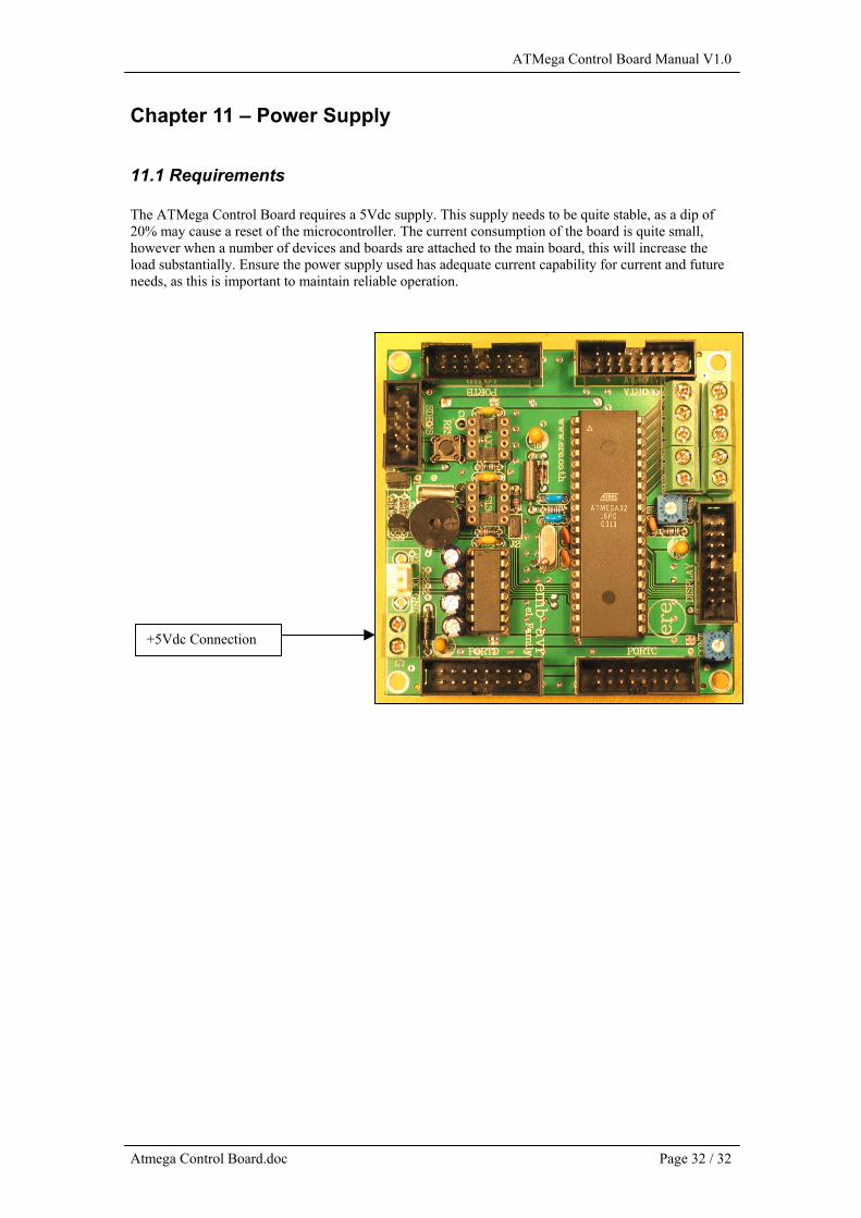
The ATMega Control Board requires a 5Vdc supply. This supply needs to be quite stable, as a dip of20% may cause a reset of the microcontroller. The current consumption of the board is quite small,however when a number of devices and boards are attached to the main board, this will increase theload substantially. Ensure the power supply used has adequate current capability for current and futureneeds, as this is important to maintain reliable operation.
+5Vdc Connection