authenticated encryption on fpgas from the reconfigurable ... · khalil, yasser yousry, tamer...
TRANSCRIPT

Authenticated Encryption on FPGAs from the
Reconfigurable Part to the Static Part
Karim Moussa Ali Abdellatif
To cite this version:
Karim Moussa Ali Abdellatif. Authenticated Encryption on FPGAs from the ReconfigurablePart to the Static Part. Cryptography and Security [cs.CR]. Universite Pierre et Marie Curie- Paris VI, 2014. English. <NNT : 2014PA066660>. <tel-01158431>
HAL Id: tel-01158431
https://tel.archives-ouvertes.fr/tel-01158431
Submitted on 1 Jun 2015
HAL is a multi-disciplinary open accessarchive for the deposit and dissemination of sci-entific research documents, whether they are pub-lished or not. The documents may come fromteaching and research institutions in France orabroad, or from public or private research centers.
L’archive ouverte pluridisciplinaire HAL, estdestinee au depot et a la diffusion de documentsscientifiques de niveau recherche, publies ou non,emanant des etablissements d’enseignement et derecherche francais ou etrangers, des laboratoirespublics ou prives.

THESE DE DOCTORAT DE L’UNIVERSITE PIERRE ETMARIE CURIE
Specialite: Informatique, Telecommunication et Electronique
Ecole Doctorale Informatique, Telecommunication et Electronique
Presentee par:
Karim Moussa Ali Abdellatif
Pour obtenir le grade de
Docteur de l’Universite Pierre et Marie Curie
CHIFFREMENT AUTHENTIFIE SUR FPGAs DE LA PARTIERECONFIGURABLE A LA PARTIE STATIC
Soutenue le 07/10/2014
devant le jury compose de:
M. Bruno Robisson ENSM.SE/CEA RapporteurM. Lilian Bossuet Laboratoire Hubert Curien RapporteurM. Jean-Claude Bajard LIP6 ExaminateurM. Hayder Mrabet FLEXRAS ExaminateurM. Olivier Lepape NanoXplore ExaminateurM. Habib Mehrez LIP6 Directeur de theseMme. Roselyne.Chotin-Avot LIP6 Encaderante de these
Ph.D. THESIS OF THE PIERRE AND MARIE CURIEUNIVERSITY
Departament: Electronics, Telecommunications and Computer Science
Presented by:
Karim Moussa Ali Abdellatif
Submitted to obtain the Ph.D. degree from:
University of Pierre and Marie Curie
Authenticated Encryption on FPGAs from the ReconfigurablePart to the Static Part
Defense date: 07/10/2014
Committee in charge:
M. Bruno Robisson ENSM.SE/CEA ReviewerM. Lilian Bossuet Laboratoire Hubert Curien ReviewerM. Jean-Claude Bajard LIP6 ExaminerM. Hayder Mrabet FLEXRAS ExaminerM. Olivier Lepape NanoXplore ExaminerM. Habib Mehrez LIP6 Thesis AdvisorMme. Roselyne.Chotin-Avot LIP6 Thesis Co-Advisor

Abstract
Communication systems need to access, store, manipulate, or communicate
sensitive information. Therefore, cryptographic primitives such as hash func-
tions and block ciphers are deployed to provide encryption and authentica-
tion. Recently, techniques have been invented to combine encryption and
authentication into a single algorithm which is called Authenticated Encryp-
tion (AE). Combining these two security services in hardware produces better
performance compared to two separated algorithms since authentication and
encryption can share a part of the computation. Because of combining the
programmability with the performance of custom hardware, FPGAs become
more common as an implementation target for such algorithms.
The first part of this thesis is devoted to efficient and high-speed FPGA-based
architectures of AE algorithms, AES-GCM and AEGIS-128, in order to be
used in the reconfigurable part of FPGAs to support security services of com-
munication systems. Our focus on the state of the art leads to the introduction
of high-speed architectures for slow changing keys applications like Virtual
Private Networks (VPNs). Furthermore, we present an efficient method for
implementing the GF(2128) multiplier, which is responsible for the authenti-
cation task in AES-GCM, to support high-speed applications. Additionally,
an efficient AEGIS-128 is also implemented using only five AES rounds. Our
hardware implementations were evaluated using Virtex-5 and Virtex-4 FP-
GAs. The performance of the presented architectures (Thr./Slices) outper-
forms the previously reported ones.

ii
The second part of the thesis presents techniques for low cost solutions in
order to secure the reconfiguration of FPGAs. We present different ranges of
low cost implementations of AES-GCM, AES-CCM, and AEGIS-128, which
are used in the static part of the FPGA in order to decrypt and authenticate
the FPGA bitstream. Presented ASIC architectures were evaluated using 90
and 65 nm technologies and they present better performance compared to the
previous work.
Keywords– Authenticated Encryption, FPGAs, ASIC, Secure Reconfigura-
tion.

iii
To the memory of my father ..

Acknowledgements
After seemingly endless days of typing and correcting, the time has come to
write the last part of this thesis. I will take this opportunity to thank several
people who have greatly influenced the journey leading to this dissertation.
First of all, great appreciation goes to my supervisors Prof. Habib Mehrez
and Dr. Roselyne Chotin-Avot for giving me the chance to do the PhD degree
in LIP6. I am grateful for the freedom I have been given during my research
and the guidance provided when needed.
I would like to extend my gratitude to Prof. Hesham Hamed, Prof. Hassan
Aboushady, Dr. Alp Kilic and Vinod Pangracious for their valuable sup-
port along the way. A great thank you goes to Akram Malak, Dr. Raouf
Khalil, Yasser Yousry, Tamer Badran, Alhassan Sayed, Mohamed Shaaban,
and Mootaz Allam for making working hours more enjoyable.
Besides my colleagues, I appreciate the care and support of my good friends,
who always managed to move my thoughts away from work when needed like
Ahmed Nabil, Mahmoud Borcan, Ahmed Nadi, and Bahaa Elmasry.
Finally, I would like to thank my parents to whom I owe a great deal. To
my late father Moussa Abdellatif, thank you for showing me that the key to
immortality is to live a life worth remembering. Very special thanks and a lot
of love go to my wife Nouranne Fahhim who always motivated and supported
me with great enthusiasm.
For all our freedom martyrs, Egypt 25/01/2011
iv

Contents
Abstract i
Acknowledgements iv
Contents v
List of Figures vii
List of Tables ix
1 Introduction 1
1.1 Motivation . . . . . . . . . . . . . . . . . . . . . . . . . . . . . 1
1.1.1 Authenticated Encryption . . . . . . . . . . . . . . . . 1
1.1.2 FPGAs . . . . . . . . . . . . . . . . . . . . . . . . . . 3
1.2 Contributions . . . . . . . . . . . . . . . . . . . . . . . . . . . 6
1.3 Thesis organization . . . . . . . . . . . . . . . . . . . . . . . . 8
I High Speed FPGA-based AE Architectures 10
2 Authenticated Encryption 11
2.1 Introduction . . . . . . . . . . . . . . . . . . . . . . . . . . . . 11
2.2 Advanced Encryption Standard (AES) . . . . . . . . . . . . . 12
2.2.1 Algorithm specifications . . . . . . . . . . . . . . . . . 12
2.2.2 Hardware implementation . . . . . . . . . . . . . . . . 16
2.3 AES-CCM . . . . . . . . . . . . . . . . . . . . . . . . . . . . . 19
2.3.1 Algorithm specifications . . . . . . . . . . . . . . . . . 19
2.3.2 Hardware implementation . . . . . . . . . . . . . . . . 21
2.4 AES-GCM . . . . . . . . . . . . . . . . . . . . . . . . . . . . . 22
2.4.1 Algorithm specifications . . . . . . . . . . . . . . . . . 23
2.4.2 Hardware implementation . . . . . . . . . . . . . . . . 25
2.5 AEGIS . . . . . . . . . . . . . . . . . . . . . . . . . . . . . . . 30
2.5.1 Algorithm specifications . . . . . . . . . . . . . . . . . 30
v

Contents vi
2.6 Conclusion . . . . . . . . . . . . . . . . . . . . . . . . . . . . . 36
3 High Speed Authenticated Encryption for Slow Changing KeyApplications Using FPGAs 37
3.1 Introduction . . . . . . . . . . . . . . . . . . . . . . . . . . . . 37
3.2 High Speed AES-GCM Architectures Using FPGAs . . . . . . 38
3.2.1 Efficient Parallel AES-GCM cores . . . . . . . . . 44
3.3 Bitstream security of the proposed architectures . . . . 49
3.4 Hardware comparison . . . . . . . . . . . . . . . . . . . . . . . 51
3.5 Conclusion . . . . . . . . . . . . . . . . . . . . . . . . . . . . . 54
4 Efficient and High Speed Key-Independent AES-Based Au-thenticated Encryption Architectures Using FPGAs 55
4.1 Introduction . . . . . . . . . . . . . . . . . . . . . . . . . . . . 55
4.2 Efficient KOA-Based GHASH . . . . . . . . . . . . . . . . . . 56
4.3 High speed AES-GCM . . . . . . . . . . . . . . . . . . . . . . 61
4.4 Efficient hardware implementation for AEGIS-128 . . . . . . . 63
4.5 Hardware comparison . . . . . . . . . . . . . . . . . . . . . . . 66
4.6 Conclusion . . . . . . . . . . . . . . . . . . . . . . . . . . . . . 70
II Low Cost Solutions for Secure FPGA Reconfigu-ration 71
5 Low Cost Solutions for Secure FPGA Reconfiguration 72
5.1 Introduction . . . . . . . . . . . . . . . . . . . . . . . . . . . . 72
5.2 FPGA reconfiguration . . . . . . . . . . . . . . . . . . . . . . 73
5.3 Previous work . . . . . . . . . . . . . . . . . . . . . . . . . . . 75
5.4 Low cost AE architecture for secure reconfiguration . . . . . . 81
5.4.1 Proposed AES-CCM . . . . . . . . . . . . . . . . . . . 83
5.4.2 Proposed AES-GCM . . . . . . . . . . . . . . . . . . . 87
5.4.3 Proposed AEGIS-128 . . . . . . . . . . . . . . . . . . . 92
5.5 Hardware comparison . . . . . . . . . . . . . . . . . . . . . . . 97
5.6 Conclusion . . . . . . . . . . . . . . . . . . . . . . . . . . . . . 100
6 Summary and Future Work 102
6.1 Thesis Summary . . . . . . . . . . . . . . . . . . . . . . . . . 102
6.2 Future work . . . . . . . . . . . . . . . . . . . . . . . . . . . . 103
List of Figures
1.1 Two separated algorithms for encryption and authentication . 2
1.2 Authenticated encryption . . . . . . . . . . . . . . . . . . . . 3
1.3 Reprogrammability using bitstream . . . . . . . . . . . . . . . 4
1.4 Reconfigurable part (user part) architecture . . . . . . . . . . 5
1.5 FPGA reconfiguration using NVM . . . . . . . . . . . . . . . . 5
1.6 Thesis contribution . . . . . . . . . . . . . . . . . . . . . . . . 6
2.1 AES algorithm . . . . . . . . . . . . . . . . . . . . . . . . . . 14
2.2 Key expansion of AES-128 . . . . . . . . . . . . . . . . . . . . 15
2.3 (a) Iterative design. (b) Pipelined design . . . . . . . . . . . . 18
2.4 AES-CCM . . . . . . . . . . . . . . . . . . . . . . . . . . . . . 21
2.5 AES-GCM . . . . . . . . . . . . . . . . . . . . . . . . . . . . . 24
2.6 Polynomial Multiplication using KOA . . . . . . . . . . . . . . 27
2.7 (a) KOA based GHAH. (b) Pipelined KOA based GHASH . . 28
2.8 The state update function of AEGIS-128 . . . . . . . . . . . . 33
3.1 Key-synthesized AES . . . . . . . . . . . . . . . . . . . . . . . 40
3.2 SubBytes implementation with BlockRAMs (a), with LUTs (b),with composite field approach (c) . . . . . . . . . . . . . . . . 41
3.3 GF(2128) multiplier proposed by [1] . . . . . . . . . . . . . . . 42
3.4 Proposed key-synthesized AES-GCM . . . . . . . . . . . . . . 43
3.5 GHASH operation . . . . . . . . . . . . . . . . . . . . . . . . 44
3.6 Proposed parallel GHASHs with fixed operand during runningtime operation . . . . . . . . . . . . . . . . . . . . . . . . . . . 46
3.7 4-parallel AES-GCM using key-synthesized method . . . . . . 48
3.8 Secure bitstream communication . . . . . . . . . . . . . . . . . 50
3.9 Hardware comparison on Virtex4 . . . . . . . . . . . . . . . . 53
4.1 Proposed pipelined KOA-based GHASH . . . . . . . . . . . . 59
4.2 Proposed AES-GCM architecture . . . . . . . . . . . . . . . . 62
4.3 Proposed high speed AEGIS-128 architecture . . . . . . . . . . 65
4.4 Hardware comparison on Virtex-5 . . . . . . . . . . . . . . . . 69
5.1 Remote reconfiguration . . . . . . . . . . . . . . . . . . . . . . 74
5.2 Cloning attack . . . . . . . . . . . . . . . . . . . . . . . . . . . 74
vii

List of Figures viii
5.3 Reverse engineering attack . . . . . . . . . . . . . . . . . . . . 75
5.4 Tampering attack . . . . . . . . . . . . . . . . . . . . . . . . . 75
5.5 Bitstream encryption/decryption by [2] . . . . . . . . . . . . . 77
5.6 Bitstream encryption . . . . . . . . . . . . . . . . . . . . . . . 79
5.7 Bitstream encryption and authentication in Virtex6 . . . . . . 80
5.8 our Proposed approach . . . . . . . . . . . . . . . . . . . . . . 83
5.9 1/4 round-based AES . . . . . . . . . . . . . . . . . . . . . . . 84
5.10 Proposed AES-CCM (encryption and authentication) . . . . . 85
5.11 Proposed AES-CCM (decryption and authentication) . . . . . 86
5.12 Proposed GF(2128) multiplier . . . . . . . . . . . . . . . . . . 88
5.13 Proposed AES-GCM (encryption and authentication) . . . . . 89
5.14 Proposed AES-GCM (decryption and authentication) . . . . . 91
5.15 (a) Full AES-round. (b) (1/4) AES-round . . . . . . . . . . . 93
5.16 Proposed AEGIS-128 architecture (encryption and authentica-tion) . . . . . . . . . . . . . . . . . . . . . . . . . . . . . . . . 95
5.17 Proposed AEGIS-128 architecture (decryption and authentica-tion) . . . . . . . . . . . . . . . . . . . . . . . . . . . . . . . . 96
5.18 Area Comparison using 90 nm technology . . . . . . . . . . . 100

List of Tables
2.1 Hardware comparison . . . . . . . . . . . . . . . . . . . . . . . 19
2.2 Hardware comparison of the previous AES-CCM architectures 22
2.3 Data flow control for GHASH calculation by [3] . . . . . . . . 29
2.4 Hardware comparison of the previous AES-GCM architectureson FPGAs . . . . . . . . . . . . . . . . . . . . . . . . . . . . . 31
3.1 Precomputed round keys . . . . . . . . . . . . . . . . . . . . . 39
3.2 Hardware comparison . . . . . . . . . . . . . . . . . . . . . . . 52
4.1 Hardware comparison . . . . . . . . . . . . . . . . . . . . . . . 67
5.1 Hardware comparison . . . . . . . . . . . . . . . . . . . . . . . 81
5.2 Previous work summery . . . . . . . . . . . . . . . . . . . . . 82
5.3 Hardware comparison . . . . . . . . . . . . . . . . . . . . . . . 98
5.4 Configuration throughput of some FPGA family members . . 100
ix

Chapter 1
Introduction
In this chapter, we introduce the overall motivation for this work and describe
the contributions. Furthermore, we outline the principal organization of the
core chapters.
1.1 Motivation
1.1.1 Authenticated Encryption
In our growing world of technology, the amount of information that we share
with the rest of the digital universe is constantly increasing. Our demands
to conceal confidential data are therefore being strongly needed and become
very important. The protection of a message includes the protection of con-
fidentiality and authenticity. There are two main approaches to authenticate
and encrypt a message:
1. The first approach is to treat the encryption and the authentication sep-
arately. A block cipher or stream cipher is used to encrypt the plaintext,
and a Message Authentication Code (MAC) is used to authenticate the
1

Chapter 1. Introduction 2
message as shown in Fig. 1.1. For example, we may use Advanced
Encryption Standard (AES) [4] for encryption, and then apply Pelican
Message Authentication Code (Pelican-MAC) [5] or Hash Message Au-
thentication Code (HMAC) [6] to the message to generate the MAC. The
encryption algorithm encrypts the message using a certain key (key1) to
provide the encrypted message. The authentication algorithm generates
the MAC using another key (key2) to provide the receiver with the en-
tity of the sender (authentication). The receiver decrypts the encrypted
message with the same key (key1) and authenticates the message (MAC
computation) using key2 to compare it with the sent MAC in order to
detect if they are equal or not.
Authentication
Decryption
Key1
Key2
Computed
Match? Y/NMAC
MAC
Message
Receiver
Message
Key1
Encryption
Message
Authentication
Sender
Key2
Insecure Channel
MA
C
Encrypted Message
Encrypted
Message
Match?
Figure 1.1: Two separated algorithms for encryption and authentication
2. Another approach is to apply an integrated Authenticated Encryption
(AE) algorithm to the message to provide both encryption and authen-
tication. One can expect that this is more efficient since encryption and
authentication can share a part of the computation. AE algorithms use
only one key for encryption and authentication as shown in Fig. 1.2.
Therefore, the key exchange and storage issues are better compared to
using two separated algorithms.
AE has been used in many widely standards such as Secure Shell (SSH) [7],
Secure Sockets Layer / Transport Layer Security (SSL/TLS) [8], IPsec [9], and
IEEE 802.11 (Wi-Fi) [10]. This has made AE very important in protocols to
secure the fundamentals of the information and communication infrastructure.

Chapter 1. Introduction 3
Encrypted Message
MA
C
Authenticated
Encryption
Computed MAC
Key1
Y/NMatch?MAC
MessageMessage
Receiver
Message
Sender
AuthenticatedEncryption
Key1
Insecure Channel
Encrypted
Figure 1.2: Authenticated encryption
There are now two NIST recommended modes of operation for authenticated
encryption, namely, Counter with Cipher Block Chaining Mode (CCM) [11]
and Galois Counter Mode (GCM) [12]. Quite some AE schemes have been
proposed, and more are expected to join the ranks with the ongoing CAE-
SAR1. The CAESAR competition is a move towards selecting a portfolio of
AE schemes that should improve upon the state of the art. AEGIS [13] is
considered one of the submitted proposals to CAESAR.
Software realizations of such algorithms have the advantage that they are
portable to multiple platforms. In general, they have a fast time to market.
However, they can be applied in systems with limited traffic at low encryp-
tion rates. Moreover, software-based applications are not power efficient com-
pared to specialized hardware architectures. Speed and power are two major
drawbacks that motivate the hardware design exploitation of cryptographic
primitives.
1.1.2 FPGAs
The increasing costs of silicon technology have put considerable pressure on
developing dedicated SoC solutions. This means that the technology will be
used increasingly for high-volume or specialist markets. Recently, Field Pro-
grammable Gate Arrays (FPGAs) have been proposed as a hardware tech-
nology for communication systems as they offer the capability to develop the
1Competition for Authenticated Encryption: Security, Applicability, and Robustness.

Chapter 1. Introduction 4
most suitable circuit architecture of the application in a similar way to SoC
systems. Compared to a full custom ASIC design, they are cost efficient, eas-
ier to manage and can immediately be put into operation. Furthermore, they
can continuously be reprogrammed during and after the design.
In order to redefine the functionality of the FPGA, a bitstream configuration
file is uploaded on the FPGA. The reconfiguration includes downloading this
bitstream file which contains the new design on the FPGA. As shown in Fig.
1.3, the bitstream is processed by the static part (configuration logic) which is
not programmable. After that, the Static Random Access Memory (SRAM)
is programmed by the processed bitstream. By programming SRAM cells, the
functionality on the FPGA reconfigurable part (user part) can be tailored to
implement the new design.
000010011100110101101001
Application
User Logic
SR
AM
Mem
ory
C
ells
Static Part
FPGA
Bitstream
Figure 1.3: Reprogrammability using bitstream
Configurable Logic Blocks (CLBs), interconnections, and embedded compo-
nents (like Block Rams (BRAMs) and Digital Signal Processing (DSP) units)
shown in Fig. 1.4 are established by programming SRAM cells to connect
fabricated routing wires together.
SRAM-based FPGAs such as those manufactured by Xilinx and Altera com-
prise the largest fraction of the overall market. Because SRAM memory is
volatile, SRAM cells must be loaded with configuration data each time the
device powers up. Configuration data is typically transmitted from an exter-
nal memory source (Non Volatile Memory (NVM)) (see Fig. 1.5), such as a
flash memory or a configuration device, to the FPGA.
In recent years, FPGAs manufacturers have come closer towards filling the
performance gap between FPGAs and ASICs, enabling them, not only to
serve as fast prototyping but also to become active players as components in

Chapter 1. Introduction 5
I/O
I/O
I/O
I/O
I/O
I/O
I/O
I/O
I/OI/OI/OI/OI/O
I/OI/OI/OI/OI/O
CLB
CLB
CLB
CLB
CLBCLB
CLB
CLB
CLB
CLB
CLB
CLB
I/O Pads
Configurable Logic Block
Embedded Components
RoutingResources
Figure 1.4: Reconfigurable part (user part) architecture
Application
User Logic
SR
AM
Mem
ory
C
ells
Static Part
FPGA
Bitstream
Non Volatile
Memory (NVM)
Figure 1.5: FPGA reconfiguration using NVM
embedded systems. As an example, Virtex-5 family [14] of FPGAs has 2400-
25920 CLBs, 1152-11664 Kb BRAMs, 8-24 multi-Gigabit transceivers, 32-640
DSP slices, 4-12 digital clock managers, and 2-6 PLL clock generators. Thus,
FPGAs are integral parts in embedded system design.

Chapter 1. Introduction 6
1.2 Contributions
This thesis deals principally with the design of efficient hardware implemen-
tations of cryptographic algorithms for encryption and authentication. We
propose FPGA and application-specific ASIC implementations that target a
wide range of different applications.
In particular, we focus on the hardware design of current AE algorithms. Fig.
1.6 shows the main contributions of this thesis. We investigate new efficient
and high speed FPGA-based architectures of AE algorithms which will be
in the user part (reconfigurable part) of the FPGA. Also, with the gathered
knowledge, we define a framework to present different ranges of low cost ASIC
architecture of AE algorithms which are inserted in the static part in order to
protect the Intellectual Property (IP) of FPGA Bitstreams.
User Logic
SR
AM
Mem
ory
C
ells
Static Part
Match?
Low Cost AE
Y/N
High Speed AE
FPGA
ComputedMAC
Encrypted Bitstream
MA
C
Memory (NVM)
Non Volatile
MAC
EncryptedBitstream
Figure 1.6: Thesis contribution
The contributions of this thesis can be summarized in the following points:
• High speed AE for slow changing key applications on FPGAs
– Algorithms for authenticated encryption are the most suitable solu-
tion to reliably secure a network link. AES-GCM has been utilized
in various security-constrained applications. VPNs are widely em-
ployed to connect private local area networks to remote locations.
VPNs use AES-GCM for encryption and authentication. Current
commercial security appliances of VPNs allow a throughput from
40 to 60 Gbps [15, 16]. We describe the benefits of VPNs as be-
ing a slow changing key environment in order to design efficient
high speed architectures. In addition, we present a solution for the

Chapter 1. Introduction 7
parallelization of AES-GCM cores in order to support applications
up to 100 Gbps. Moreover, we present a protocol to secure the
reconfiguration of the proposed architectures on FPGAs.
• FPGA-based high performance AES-GCM using Efficient GF (2128)
multiplier
– The performance of AES-GCM is always determined by the GF(2128)
multiplier (authentication part) because of the inherent computa-
tion feedback. We introduce an efficient pipelined Karatsuba Of-
man Algorithm (KOA) for the GF(2128) multiplier to support high
speed applications. In particular, the computation feedback is re-
moved by analyzing the complexity of the computation process.
The proposed GF(2128) multiplier is evaluated with the pipelined
AES in order to support high speed applications.
• Efficient hardware implementation for AEGIS
– Pushed by our involvement into the hardware design of efficient
AE algorithms, we decided to follow the CAESAR competition by
designing high speed architecture of AEGIS which was accepted to
the first round of the CAESAR competition.
All presented architectures in these contributions aim at applications
with high demands for data throughput and performance. For these
designs, we primarily employ Xilinx Virtex-4 and Virtex-5 FPGAs as
an implementation target. Our proposed high speed architectures pro-
vide most savings in logic and routing resources with the highest data
throughput on FPGAs compared to previous work reported in open lit-
erature.
• Low cost solutions for IP protection of FPGA bitstreams
– IPs loaded on the FPGAs represent a kind of investment that
requires protection especially in case of remote reconfiguration.
Therefore, the FPGA must accept encrypted bitstreams from au-
thorized entities. We present different low cost solutions for per-
forming decryption and authentication of bitstreams. Efficient and

Chapter 1. Introduction 8
compact ASIC AE architectures, AES-CCM, AES-GCM, and AEGIS,
are added in the static part of the FPGA to support encrypted and
authenticated bitstreams.
Presented ASIC architectures were evaluated by using 90 and 65 nm
technologies. Our comparison to previous work reveals that our archi-
tectures are more area-efficient.
1.3 Thesis organization
The outline of this thesis is as follows:
• Chapter 2 gives detailed overview about current AE algorithms. AES-
CCM, AES-GCM, and AEGIS are discussed in detail. Later in the
chapter, we highlight the previous work that covers the hardware imple-
mentations of AE algorithms.
• Chapter 3 is entirely dedicated to high speed AES-GCM architectures
for slow changing key applications like VPNs. It presents an efficient
method for the parallelization of AES-GCM cores on FPGAs. Further-
more, we propose a protocol to protect the bitstream of the proposed
architectures on FPGAs.
• Chapter 4 presents an efficient method for the GF (2128) multiplier
used in AES-GCM. By focusing on the drawbacks of the previous ar-
chitectures of GF (2128) multipliers, we propose an efficient method to
remove the computation feedback in the GF (2128) multiplier. This is
accomplished by the presented pipelined Karatsuba Ofman Algorithm
(KOA)-based GF (2128). Finally, an efficient high speed architecture of
AEGIS is also presented in this chapter.
• Chapter 5 starts with an overview of security issues used in reconfigu-
ration of FPGAs and analyze how well they are suited to IP protection
of FPGA bitstreams. Later in this chapter, low cost implementations of
AE algorithms are presented for FPGA bitstreams protection.

Chapter 1. Introduction 9
• Chapter 6 summarizes the thesis and points out some future work.
Part I
High Speed FPGA-based AE
Architectures
10

Chapter 2
Authenticated Encryption
2.1 Introduction
Originally, confidentiality and authenticity services have been implemented
separately, by using two different algorithms. Encryption algorithms are used
to ensure confidentiality while Message Authentication Codes (MACs) can be
used to provide authentication. When two separated algorithms are used to
provide independent security services, it is considered cryptographically secure
to use separated keys for each algorithm. Recently, techniques have been
invented to combine encryption and authentication into a single algorithm
which is called Authenticated Encryption (AE). Combining these two security
services in hardware might support the following advantages:
• Area requirement for a single algorithm could be smaller compared to
two separated algorithms because encryption and authentication can
share a part of the computation.
11
Chapter 2. Authenticated Encryption 12
• A slight advantage regarding key management and key storage issues
because AE needs only a single key for both encryption and authentica-
tion.
The following is a brief overview of the most popular AE algorithms that have
been developed as a result of the current research. The aim is to provide the
details of AE algorithms to allow the reader to understand and analyze each
algorithm. Also, for each algorithm, we present the previous work in terms of
the hardware implementation in order to highlight the current challenges of
the state of the art.
The most common way of constructing an AE scheme is a mode of operation
for a block cipher, like AES [4]. Therefore, in order to discuss AE algorithms
clearly, it is useful to highlight AES because it is common in all AE schemes
that we will present.
2.2 Advanced Encryption Standard (AES)
For the drawbacks of the previous symmetric-key cryptographic standards
such as the DES and the 3DES, they have been replaced by the Advanced
Encryption Standard (AES) [4]. In particular, the AES has overcome the
drawbacks of the previous standards in terms of vulnerability to brute force
attacks and slow software implementations. The AES was accepted by the
National Institute of Standards and Technology (NIST) in 2001 and since its
acceptance, it has been utilized in a variety of security-constrained applications
like IEEE 802.11i standard [17]. It is considered by industry and government
environments as the essential scheme to protect sensitive information.
2.2.1 Algorithm specifications
The AES algorithm is a symmetric-key cipher, in which both the sender and
the receiver use a single key for encryption and decryption. The data block
length is fixed to be 128 bits, while the key length can be 128, 192, or 256

Chapter 2. Authenticated Encryption 13
bits. It is an iterative algorithm. Each iteration can be called a round, and
the total number of rounds, N, is 10, 12, or 14, when the key length is 128,
192, or 256 bits, respectively.
The 128-bit data block is divided into 16 bytes. These bytes are mapped to
a 4 × 4 array called the State, and all the internal operations of the AES
algorithm are performed on the State. Each byte in the State is detonated by
S(i,j) (0 ≤ i ≤ 3, 0 ≤ j ≤ 3) and is considered as an element of GF (28) with
P (x) = x8 + x4 + x3 + x + 1 as an irreducible polynomial. Fig. 2.1 shows the
block diagram of the AES algorithm.
In the encryption of the AES algorithm, each round except the final round
consists of four transformations in a fixed order:
1. SubBytes is a non-linear transformation that substitutes the bytes of
the state independently, using a s-box built over two steps: computa-
tion of the multiplicative inverse in the Galois field GF (28) followed by
an affine transformation in GF(2). The SubBytes can be described as
follows:
S(i, j) = MS−1i,j + C (2.1)
where M is an 8 × 8 binary matrix, S−1 is the multiplicative inverse of
the input, and C is an 8-bit binary vector with only 4 nonzero bits.
2. ShiftRows is a simple shifting transformation. The first row of the State
does not change, while the second, third and fourth rows cyclically shift
one byte, two bytes and three bytes to the left, respectively
3. MixColumns multiplies in GF (28) each column of the of the State (4
bytes) with a(x) modulo x4 + 1 where
a(x) = 03x3 + 01x2 + 01x + 02. (2.2)
4. AddRoundKey adds a round key to the state in GF(2).

Chapter 2. Authenticated Encryption 14
++ ++
Mix Columns
+ + + + + + + + + + +
Mix Columns
0 1 2 3 4 5 6 7 8 9 10 11 12 1413 15
Mix Columns Mix Columns
+
0 1 2 3 4 5 6 7 8 9 10 11 12 1413 15
Cip
her
text
(C)128
128
Pla
inte
xt
Add R
ound K
ey
Round 1
Round 2
Round N
Key Schedule
128/192/256
Key
Mix Columns
S S S S S S S S S S S S SS S S
16 input Bytes
16 output Bytes
SubBytes()
MixColumns()
AddRoundKey()
12
8
12
8
12
8
k0 k1 k2 k N
Figure 2.1: AES algorithm
The AES round is completed with the key expansion (see Fig. 2.2), which
generates the round keys from the original key. This expansion is defined on
4-bytes words and mainly uses the transformations of the round. A single
round key is made up by four words and is updated to the next round key
using g function which combines the SubWord (s-box over a 4-byte input)
and RotWord (word shift) functions. The rest of the key parts are generated
using XOR function.

Chapter 2. Authenticated Encryption 15
k k k k k k k k k k
0 1 2 3 4 5 6 7 8 9 10 15k k11 k12 k13 k14 k
W[0] W[2]W[1] W[3]
g
W[4] W[5] W[6] W[7]
32 32 32 32
32323232
Figure 2.2: Key expansion of AES-128
The transformations in the decryption process perform the inverse of the cor-
responding transformations in the encryption process.
1. InvSubBytes performs the inverse of the SubBytes stage as follows:
S(i, j) = (MS−1i,j + C)−1. (2.3)
2. InvShiftRows does not change the first row, while the rest of the
rows are cyclically shifted to the right by the same offset as that in
the ShiftRows.
3. InvMixColumns multiplies the polynomial formed by each column of
the State with a(x)−1 modulo x4 + 1, where
a(x) = 0bx3 + 0dx2 + 09x + 0e. (2.4)

Chapter 2. Authenticated Encryption 16
4. AddRoundKey adds a round key to the state in GF(2), while the
round keys are computed in the reverse order within the key expansion
process.
2.2.2 Hardware implementation
After the standardization of AES, several research contributions focusing on
hardware implementations of the algorithm have been presented. Nowadays,
almost each possible AES architecture, covering the entire design space (both
in ASIC and FPGA), has been investigated. Companies and federal organi-
zations have plenty of choice in selecting the suitable design.
We list the major components and strategies that characterize the AES hard-
ware design:
• Datapath: AES is defined by 128-bit state with 8-bit operations. As
a result, the designer has the choice to adapt or shrink the datapath
of his architecture according to the system specification. Typical dat-
apath widths are 128, 64, 32, 16, or 8 bits. The datapath size affects
directly the area occupation and the final throughput of the AES core.
It represents a sort of area/speed trade-off. In [18], the authors analyze
different-datapath implementations on FPGAs.
• Round components: The SubBytes transformation is the most costly
(both in size and propagation delay) component of the AES round. In
terms of the ShiftRows operation, it does not consume any logic because
it is implemented as a straightforward routing of the signals without
any specific hardware component, while the most efficient strategy to
realize MixColumns is with the combinational logic as shown in [19].
Several approaches to design the SubBytes have been developed and
implemented. We describe briefly three main solutions:
1. Block Random Access Memory (BRAMs)
The s-box is implemented as a Look Up Table (LUT) and stored
in a dedicated memory. This approach is particularly suitable for

Chapter 2. Authenticated Encryption 17
modern FPGAs, which contain BRAMs. This approach saves the
logic area because the most consuming part (s-boxes) are imple-
mented as BRAMs (see [20])
2. Composite field
In [21], composite field arithmetic is employed to reduce the area
requirements, and different implementations for the inversion in
subfield GF (24) are compared. This reduction to composite fields
brings significant improvement in flexibility and in the area costs
of SubBytes.
3. FPGA LUT
The third approach is dedicated only to FPGA devices. The s-box
can be directly instantiated in LUTs located in the FPGA logic
elements. As example, the basic logic elements of Xilinx FPGAs
are called slices and each slice comprises a different number of LUTs
depending on the selected device. In a Xilinx Virtex-5 chip a single
s-box is implemented on 32 6-input LUTs because of 6-input LUT
technology (see [22]).
• Rolled or unrolled: The operation mode of AES influences remarkably
the performance of the implementation. Feedback modes like Cipher
Block Chaining (CBC) mode [23] lead to iterative designs, where single
round is considered to be the most efficient solution. Fig. 2.3(a) shows
the iterative design using only one round. An example of the iterative
design is shown in [22]. Because of using only one round, the throughput
of the iterative design of AES-128 presented by [22] is as follows:
Throughput(Mbps) =Fmax(Mhz)× 128
10. (2.5)
Full unrolled architectures combined with pipelining (Fig. 2.3(b)) can be
exploited only by the feedback-free modes [23] like Electronic Codebook
(ECB) and Counter (CTR) mode. Unrolled designs with pipelining are
able to achieve 20-30 Gbps, simply by putting a pipeline stage between
the rounds. To further increase the speed, pipelining can also be im-
plemented inside the round and the SubBytes operation (see [18]). The
throughput of the pipelined design is calculated as follows:

Chapter 2. Authenticated Encryption 18
Key
Sch
edu
leR
ou
nd
+
Key
Sch
edu
le
+
Ro
un
d 1
Ro
un
d 2
Ro
un
d 1
0
Key
128
128
Key
128
Pla
inte
xt
(P)
Cip
her
tex
t (C
)
Cip
her
tex
t (C
)
Pla
inte
xt
(P)
(a)
(b)
Figure2.3:
(a)
Iter
ativ
ed
esig
n.
(b)
Pip
elin
edd
esig
n

Chapter 2. Authenticated Encryption 19
Throughput(Mbps) = Fmax(Mhz)× 128. (2.6)
Table 2.1 shows the hardware hardware comparison between the iterative
design and the pipleined design. It is clear that the pipelined design
consumes more area compared to the iterative design, while the speed
is higher.
Table 2.1: Hardware comparison
Design FPGA Area (slices) Frequency ThroughputMhz Gbps
Iterative [22] Vertex-E 2257 169 2.1Pipelined [18] Spartan-III 17425 196.1 25.1
After giving an overview of AES, the following sections present the current
AE algorithms and how they are implemented on FPGAs and ASIC.
2.3 AES-CCM
Counter with Cipher Block Chaining Mode (CCM) [24] can be used in con-
junction with any approved 128-bit block cipher like AES. CCM has been
specified in the draft IEEE 802.11i standard for wireless networks. It has also
been specified in IEEE 802.15 (Wireless Personal Area Networks) and 802.16
(Broadband Wireless Metropolitan Area Networks) standards. It is designed
for packet environment, where all the data is available in storage before the
processing. This implies that it is not online.
2.3.1 Algorithm specifications
Variables:
N : 128-bit Valid nonce
A : 128-bit Associated data

Chapter 2. Authenticated Encryption 20
P : 128-bit Plaintext
C : 128-bit Ciphertext
MAC : 128-bit Message Authentication Code
L : Message length
Key:128-bit Key
Specifications:
AES-CCM has four inputs: an AES key, N, P, and A. AES-CCM generates
two outputs: C and MAC. N and A are used to verify the correctness of
the MAC. Fig. 2.4 shows the block diagram of CCM. It depends on the
block cipher AES in two modes. Cipher Block Chaining (CBC) mode for the
authentication, while the encryption is performed by Counter (CTR) mode.
A and N are not encrypted but they are authenticated in order to verify the
correctness of authentication.
Encryption and MAC generation:
1. The plaintext P is stored in a memory.
2. N, A, and P are loaded to AES in CBC mode to generate Y, this value
is used for authentication.
3. The first value of the counter is encrypted (CTR mode) to be S[0] which
is mixed with Y through XOR operation in order to generate the final
MAC.
4. Encryption is performed by CTR mode.
Decryption and MAC verification:
1. Decryption is performed by XORing C[i] with the values of the encrypted
counter S[i] to give P.
2. N, A, and P are loaded to AES in CBC mode to generate Y.
3. Y is XORed with S[0] to generate the MAC.
4. MAC verification is computed.

Chapter 2. Authenticated Encryption 21
+ +
S[i]
P[i]
C[i]
S[0]
Y
MAC
AES
S[L]
AES
KeyCTR[0]
S[0]
AES
KeyCTR[1]
S[1]
AES
KeyCTR[2]
S[2]
CTR[n] Key
AES
+ + +
AES AES AES
Key Key Key Key
Y
CBC mode
N
A p[L]
CTR mode
p[1]
Figure 2.4: AES-CCM
2.3.2 Hardware implementation
There are some research contributions focusing on the hardware implemen-
tations of AES-CCM on FPGAs and ASIC. Because of being feedback-based
algorithm (it depends on CBC mode), iterative design of AES is always used
in the hardware implementation.
In [25], iterative AES (one round) was used to implement the architecture of
AES-CCM on FPGAs and ASIC. The proposed architecture in [25] used one
AES block for doing both authentication and encryption. This manner de-
creases the consumed area because there is only one AES architecture that is
used for the two modes, CBC and CTR modes. As a result the speed of the ar-
chitecture is reduced by 2 compared to the use of two AES architectures. Two

Chapter 2. Authenticated Encryption 22
iterative components of AES were implemented for both encryption and au-
thentication on FPGAs in [26]. In [27], FPGA-based AES-CCM was presented
by using two blocks of AES and they are 32-based datapath architectures.
From the previous discussion, it is clear that AES-CCM is a feedback-based
algorithm because it depends on the CBC mode in terms of performing the
authentication task. Therefore, only iterative-based designs of AES are appli-
cable to CCM, while using pipelined designs is not. As a result, the overall
speed is limited as shown in Table 2.2.
Table 2.2: Hardware comparison of the previous AES-CCM architectures
Design Implementation Area Frequency Throughputplatform Mhz Mbps
[25] 90 nm 0.057 mm2 148 434[26] Spartan-3 633 slices 100.08 1051.5
(90 nm)[27] Spartan-3 487 slices + 4 BRAMs 247 687.3
(90 nm)
2.4 AES-GCM
Galois Counter Mode (GCM) [28] is an AE algorithm. It is well-suited for
wireless, optical, and magnetic recording systems due to its multi-Gbps au-
thenticated encryption speed, outstanding performance, minimal computa-
tional latency as well as high intrinsic degree of pipelining and parallelism.
New communication standards like IEEE 802.1ae [29] and NIST 800-38D have
considered employing GCM to enhance their performance.
It simultaneously provides confidentiality, integrity and authenticity assur-
ances on the data. It can be implemented in hardware to achieve high speeds
with low cost and low latency. It was designed to meet the need for an au-
thenticated encryption mode that can efficiently achieve speeds of 10 Gbps
and higher in hardware.

Chapter 2. Authenticated Encryption 23
2.4.1 Algorithm specifications
Operations:
The following operations are used in AES-GCM:
⊕ : bit-wise exclusive OR
‖ : concatenation
Variables:
IV: 96-bit Initialization Vector
A: 128-bit Associated data
P: 128-bit Plaintext
C: 128-bit Ciphertext
L: Message length
MAC: Message Authentication Code
Key:128-bit Key
Specifications:
AES-GCM accepts four inputs: an AES key, IV, P, and A. AES-GCM gen-
erates two outputs: C and MAC. A is used to verify the correctness of the
MAC. Fig. 2.5 shows the block diagram of AES-GCM. It contains an AES
engine in CTR mode for encryption, while the authentication is performed by
the Galois Hash (GHASH) which is composed of chained GF(2128) multipliers.
Encryption and MAC generation:
1. Generation of H by encrypting 0128 block
H = E(Key, 0128). (2.7)
2. Assigning the first value of the counter (CTR[0]) as follows:

Chapter 2. Authenticated Encryption 24
AES
Key
AESAES AES AES
+ + +
+ ++
+
GF(2128 )
Multiplier
GF(2128 )
Multiplier
GF(2128 )
Multiplier
GF(2128 )
MultiplierGF(2
128) GF(2
128) GF(2
128) GF(2
128)
"00..00" CTR[2]CTR[1]CTR[0] Key Key Key Key
H
H H H HA
P[1] P[2]
C[1] C[2]
MAC
Encryption using CTR mode
Authentication using GF multiplier
C[L]
P[L]
CTR[L]
Multiplier Multiplier Multiplier Multiplier
Figure 2.5: AES-GCM
CTR[0] =
IV ‖ 0311 If(length(IV ) = 96)
H × IV otherwise
where the multiplication between H and IV is a GF (2128)-based multi-
plication.
3. Encryption is performed by AES in CTR mode.
4. Authentication is computed by the GF (2128) multipliers chain and the
output is XORed with the encrypted value of CTR[0] in order to obtain
the final MAC.
Decryption and MAC verification:
1. Generation of H by encrypting 0128 block (Equation 2.7).
2. Assigning the first counter value (step 2 in encryption stage)
3. Decryption is performed by XORing the encrypted values of the counter
with C to obtain P.
Chapter 2. Authenticated Encryption 25
4. MAC verification is accomplished by the same scenario of the encryption
process.
2.4.2 Hardware implementation
As we presented before, two main components in AES-GCM are an AES engine
and a GF (2128) multiplier. Also, the main goal of AES-GCM is to support
high speed applications (10 Gbps and higher in hardware). Therefore, most
of the previous hardware architectures were proposed to support high speed
applications. As a result, the pipelined AES (pipelined AES implementation
has been discussed in Section 2.1) is used to perform the encryption task of
AES-GCM [3, 30, 31]. The second important part of AES-GCM is the GHASH
which depends on the inherent feedback operations chain of the GF (2128)
multipliers. Therefore, the system performance is always determined by the
GF (2128) multiplier.
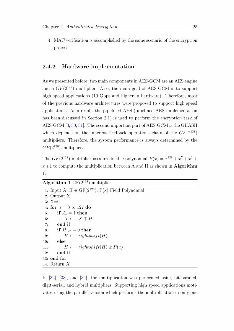
The GF (2128) multiplier uses irreducible polynomial P (x) = x128 + x7 + x2 +
x+1 to compute the multiplication between A and H as shown in Algorithm
1.
Algorithm 1 GF(2128) multiplier
1: Input A, H ∈ GF(2128), P(x) Field Polynomial2: Output X3: X=04: for i = 0 to 127 do5: if Ai = 1 then6: X ←− X ⊕H7: end if8: if H127 = 0 then9: H ←− rightshift(H)
10: else11: H ←− rightshift(H)⊕ P (x)12: end if13: end for14: Return X
In [32], [33], and [34], the multiplication was performed using bit-parallel,
digit-serial, and hybrid multipliers. Supporting high speed applications moti-
vates using the parallel version which performs the multiplication in only one

Chapter 2. Authenticated Encryption 26
clock cycle. In Algorithm 1, if H is fixed, the multiplier is called a fixed
operand GF(2128) multiplier as shown by [1]. This design proposed by [1] can
be used efficiently (smaller area) on FPGAs as the circuit is specialized for H.
The drawback in [1] is the need for a new reconfiguration in case of changing
the key.
Karatsuba Ofman Algorithm (KOA) [35] is used to reduce the complexity
(consumed area) of the GF(2128) multiplier. More precisely, the single step
KOA algorithm splits two m bit inputs A and B into four terms Ah, Al, Bh, Bl
which are m/2 bit terms. The 1-step iteration of KOA shown in Fig. 2.6 can
be described as:
Dl = Al ×Bl
Dhl = (Ah ⊕ Al)× (Bh ⊕Bl)
Dh = Ah ×Bh
D = DhXm ⊕Xm/2(Dh ⊕Dhl ⊕Dl)⊕Dl.
(2.8)
After the multiplication stage is processed using KOA, the binary field reduc-
tion step is used to convert the length of the vector from 2m−1 to m as shown
in Equation 2.9.
C(x) = D mod P (x) (2.9)
where P(x) is the field polynomial used for the multiplication operation.
KOA was used by [30] to reduce the complexity (consumed area) of the
GF(2128) multiplier as shown in Fig. 2.7(a). Because the GHASH is a chain
of the GF (2128) multipliers, the GHASH output (Fig. 2.7(a)) is calculated as
follows:
Output = (Ci ⊕ Zi−1)×H. (2.10)
The drawback of the architecture presented in [30] is the critical delay resulting
from the multiplication stage. In order to reduce the data path (critical delay)

Chapter 2. Authenticated Encryption 27
+ +
hB Bl Ah Al
Dl
Dl
Dhl
Dh
Dh
+
+
= (m/2) Multiplier
= XOR operation
Binary field reduction(mod P)
mm
m/2m/2
m/2m/2
m−1m−1
m−1
2m−1
m
B A
D
C
Figure 2.6: Polynomial Multiplication using KOA
of the KOA multiplier, pipelining concept was accomplished by [3] as shown
in Fig. 2.7(b). Equation 2.10 was written by [3] as follows:
Output = Q1 ⊕Q2 ⊕Q3 ⊕Q4, where (2.11)
Q1 = (((C1 ×H4 ⊕ C5)×H4 ⊕ C9)×H4 ⊕ ....)×H4 (2.12)
Q2 = (((C2 ×H4 ⊕ C6)×H4 ⊕ C10)×H4 ⊕ ....)×H3 (2.13)

Chapter 2. Authenticated Encryption 28
Q1
Q2
Q3
Q4
+(a)
CiCi
Z i
+
mod(p)
HH4
(b)
X Y
Z
Pip
elin
ed K
OA
Output
Output
+H
mod(p)
KOA multiplier
Figure 2.7: (a) KOA based GHAH. (b) Pipelined KOA based GHASH
Q3 = (((C3 ×H4 ⊕ C7)×H4 ⊕ C11)×H4 ⊕ ....)×H2 (2.14)
Q4 = (((C4 ×H4 ⊕ C8)×H4 ⊕ C12)×H4 ⊕ ....)×H. (2.15)
The hardware architecture proposed by [3] (Fig. 2.7(b)) is a 4-stage pipelined
KOA-based GHASH. An example of data flow control for the GHASH is shown
in Table 2.3, where C1 .... C8 is the input sequence and ”-” denotes ”don’t
care”. At the beginning, H4 is passed to port Y. After the input of C6, H is
passed to port Y. The partial GHASH values Q1, Q2, Q3, and Q4 are ready
at the 9th, 15th, 18th, and 12th clock, respectively. As shown from Table 2.3,
the multiplier output resulting from 8 frames of 128-bit is ready after 19 clock
cycles. Therefore, the real throughput is calculated as follows:

Chapter 2. Authenticated Encryption 29
Table 2.3: Data flow control for GHASH calculation by [3]
Clock Ci X Y Z Comment
1 C1 C1 H4 02 C2 C2 H4 03 C3 C3 H4 04 C4 C4 H4 05 C5 (C1 ×H4)⊕ C5 H4 C1 ×H4
6 C6 (C2 ×H4)⊕ C6 H C2 ×H4
7 C7 (C3 ×H4)⊕ C7 H C3 ×H4
8 C8 (C4 ×H4)⊕ C8 H C4 ×H4
9 - - - ((C1 ×H4)⊕ C5)H4 z = Q1
10 0 ((C2 ×H4)⊕ C6)×H H ((C2 ×H4)⊕ C6)×H11 0 ((C3 ×H4)⊕ C7)×H H ((C3 ×H4)⊕ C7)×H12 0 - - ((C4 ×H4)⊕ C8)×H z = Q4
13 0 - - -14 0 ((C2 ×H4)⊕ C6)×H2 H ((C2 ×H4)⊕ C6)×H2
15 - - - ((C3 ×H4)⊕ C7)×H2 z = Q2
16 - - - -17 - - - -18 - - - ((C2 ×H4)⊕ C6)×H3 z = Q3
19 - - - - GHASH
Throughput(Mbps) = Fmax(MHz) × 128× (8
19). (2.16)
The last component of Equation 2.16 is ( 819
), it is called the reduction factor
and the authors of [3] neglected this component in their throughput calcu-
lation. Therefore, their presented design of GHASH has not increased the
throughput as they claimed.
Henzen et al. [31] proposed 4-parallel AES-GCM using pipelined KOA. Their
design achieved the authentication of 18 frames of 128-bits in 11 clock cycles
because of the latency resulting from the pipelined KOA. As a result, their
throughput is calculated as follows:
Throughput(Mbps) = Fmax(MHz) × 128× 18
11. (2.17)
The authors of [31] neglected this component (1811
) in their throughput calcu-
lation and replaced it by 4. Hence, their presented parallel design of GHASH
has not increased the throughput by 4 as shown in Equation 2.17.

Chapter 2. Authenticated Encryption 30
Table 2.4 shows the hardware comparison of the current AES-GCM cores on
FPGAs. It is clear that the maximum throughput resulting from implementing
single AES-GCM core on FPGAs (Virtex-5) is 17.9 Gbps with 4628 slices ([3]).
In terms of the parallel cores, the maximum throughput is 48.8 Gbps ([31]).
2.5 AEGIS
The field of AE has received more interest in the light of the recently an-
nounced CAESAR (Competition for Authenticated Encryption: Security, Ap-
plicability, and Robustness). CAESAR will define a portfolio of AE algorithms
that offer advantages over AES-GCM. Secure and efficient algorithms for spe-
cific or possibly multiple environments will be presented.
There are some AE schemes have been proposed, and more are expected to join
the ranks with the ongoing CAESAR. In this section, we present an overview
on AEGIS [36] which is considered one of the candidates to CAESAR. It is
constructed from the AES encryption round function (not the last round).
AEGIS is a stream cipher with a large state which is updated continuously.
Therefore, the attacks against a block cipher cannot be applied directly to
it. The goal of AEGIS is to achieve high performance and strong security as
outlined in [36]. AEGIS-128 processes a 16-byte message block with five AES-
round functions, and AEGIS-256 uses 6 AES round functions. More precisely,
we will highlight AEGIS-128 because the thesis concentrates on 128-based AE
algorithms.
2.5.1 Algorithm specifications
Operations:
⊕ : bit-wise exclusive OR
& : bit-wise AND
‖ : concatenation
Variables and constants:

Chapter 2. Authenticated Encryption 31
Table2.4:
Har
dw
are
com
par
ison
ofth
ep
revio
us
AE
S-G
CM
arch
itec
ture
son
FP
GA
s
FP
GA
typ
eD
esig
nSubB
yte
sA
rea
(slice
s)B
RA
Ms
Max
-Fre
qT
hr.
Thr.
/Slice
MH
zG
bit
/sM
bps/
Slice
[3]
Vir
tex4
AE
S-G
CM
BR
AM
7712
8228
515
.41.
99[3
]V
irte
x4
AE
S-G
CM
Com
p.
1434
90
277
14.9
1.04
[3]
Vir
tex5
AE
S-G
CM
BR
AM
3533
4131
416
.94.
78[3
]V
irte
x5
AE
S-G
CM
Com
p64
920
314
16.9
2.60
[3]
Vir
tex5
AE
S-G
CM
LU
T46
280
324
17.5
3.77
[32]
Vir
tex4
AE
S-G
CM
BR
AM
1320
011
411
014
1.07
[32]
Vir
tex4
AE
S-G
CM
Com
p.
2160
00
9011
.52
0.53
[31]
Vir
tex5
4-par
alle
lA
ES-G
CM
BR
AM
9561
450
233
48.8
5.1
[31]
Vir
tex5
4-par
alle
lA
ES-G
CM
Com
p18
505
023
348
.82.
64[3
1]V
irte
x5
4-par
alle
lA
ES-G
CM
LU
T14
799
023
348
.83.
29

Chapter 2. Authenticated Encryption 32
The following variables and constants are used in AEGIS-128:
IV128 : The 128-bit initialization vector
P : 128-bit plaintext
C : 128-bit ciphertext
mi : 128-bit data block
const0 : The first 16 bytes of const
const1 : The second 16 bytes of const
K128 : The 128-bit key
msglen : The bit length of the plaintext
AEGIS depends on the AESRound (A,B), where A is the 16-byte state,
B is the 16-byte round key. It is performed using the AES round functions
(ShiftRows, SubBytes, MixColumns, and AddRoundKey). With a 128-bit key
and a 128-bit initialization vector, AEGIS-128 encrypts and authenticates a
message with length less than 264 bits. The authentication MAC length is less
than or equal to 128 bits. It is strongly recommend the use of a 128-bit MAC.
The state update function of AEGIS-128:
The state update function shown in Fig. 2.8 updates the 80-byte state Si with
a 16-byte message block mi.
Si+1 = StateUpdate128(Si,mi) is given as follows:
Si+1,0 = AESRound(Si,4, Si,0 ⊕mi)
Si+1,1 = AESRound(Si,0, Si,1)
Si+1,2 = AESRound(Si,1, Si,2)
Si+1,3 = AESRound(Si,2, Si,3)
Si+1,4 = AESRound(Si,3, Si,4).
(2.18)

Chapter 2. Authenticated Encryption 33
+
++
++
+SS
SS
S
SS
SS
S
i,0
i,1
i,2
i,3
i,4
i+1
,0i+
1,1
i+1
,2i+
1,3
i+1
,4
ww
Su
bB
yte
s
Sh
ift
Ro
ws
Su
bB
yte
s
Sh
ift
Ro
ws
Su
bB
yte
s
Sh
ift
Ro
ws
Su
bB
yte
sS
ub
By
tes
Sh
ift
Ro
ws
Sh
ift
Ro
ws
Mix
Co
lum
ns
Mix
Co
lum
ns
Mix
Co
lum
ns
Mix
Co
lum
ns
Mix
Co
lum
ns
mi
Figure2.8:
Th
est
ate
up
dat
efu
nct
ion
ofA
EG
IS-1
28

Chapter 2. Authenticated Encryption 34
The initialization of AEGIS-128:
The initialization of AEGIS-128 consists of loading the key and IV into the
state, and running the cipher for 10 steps with the key and IV being used as
message.
1. Load the key and IV into the state as follows:
S−10,0 = IV128
S−10,1 = Const1
S−10,2 = Const0
S−10,3 = K128 ⊕ Const0
S−10,4 = K128 ⊕ Const1.
2. For i = -5 to -1, m2i = K128, m2i+1 = K128 ⊕ IV128.
3. For i = -10 to -1, Si+1 = StateUpdate128(Si,mi).
The encryption of AEGIS-128:
After the initialization, at each step of the encryption, a 16-byte plaintext
block Pi is used to update the state, and Pi is encrypted to Ci. If the size of
the last message block is less than 128 bits, it is padded with 0 bits to a full
block, and the padded full block is used to update the state.
1. If the last plaintext block is not a full block, use 0 bits to pad it to 128
bits.
2. For i = 0 to (msglen128− 1), the state is updated to perform encryption.
Ci = Pi ⊕ Si,1 ⊕ Si,4 ⊕ (Si,2&Si,3)
Si+1 = StateUpdate128(Si, Pi).(2.19)

Chapter 2. Authenticated Encryption 35
The finalization of AEGIS-128 (MAC generation):
After encrypting all the plaintext blocks, the authentication MAC is generated
using seven more steps. The message being used at this stage is part of the
state at the end of the encryption, together with the length of the associated
data and the length of the message.
1. Let tmp = lenA‖msglen, where lenA and msglen are represented as
64-bit integers
2. For i= (msglen128
) to (msglen128
+ 6), mi = Smsglen128
,3 ⊕ tmp
3. For i= (msglen128
) to (msglen128
+ 6), the state is updated:
Si+1 = StateUpdate128(Si, Pi)
4. The authentication MAC is generated from the state msglen128
+7 as follows:
MAC = ⊕4i=0(S(msglen
128+7),i). (2.20)
The decryption and verification of AEGIS-128:
The exact values of the key and the IV should be known to the decryption
and verification process. The decryption is similar to encryption, and it is
described below:
1. For i = 0 to (msglen128−1), the state is updated to perform the decryption.
Pi = Ci ⊕ Si,1 ⊕ Si,4 ⊕ (Si,2&Si,3)
Si+1 = StateUpdate128(Si, Pi).(2.21)
2. The finalization in the decryption process is the same as that in the
encryption process (authentication).

Chapter 2. Authenticated Encryption 36
In terms of the hardware implementation, to our knowledge, there is no any
current hardware implementation for AEGIS.
2.6 Conclusion
In this chapter, we highlighted current AE algorithms, AES-CCM, AES-GCM,
and AEGIS. Each algorithm was presented in detail and also followed by
the current hardware implementations. Regarding AES-CCM, we showed the
disadvantages of AES-CCM. It is not suitable for online applications as the
message must be stored first before performing the authentication and the
encryption. Also, it is not suited to high-speed implementations, because
CBC-MAC is neither pipelinable nor parallelizable (see Table 2.2). In terms
of AES-GCM, four different FPGAs-based architectures have been presented
in the open literature ([32],[30],[3],[31]). It is clear that these contributions
do generally have common challenge related to the throughput of their archi-
tectures (see Equation 2.16, Equation 2.17, and Table 2.4). Additionally, we
presented an overview of AEGIS which is considered one of the candidates to
CAESAR. Till now, there is no any hardware implementation for AEGIS.

Chapter 3
High Speed Authenticated
Encryption for Slow Changing
Key Applications Using FPGAs
3.1 Introduction
Virtual Private Networks (VPNs) offer an economic alternative to leased lines
for building a private network. It is set up by allowing users to tunnel through
the public network in a manner that manages the tunnel participants to enjoy
a secure connection if they are on a typical private network. VPN tunnels
can be either static (between two routers) or dynamic (between end-users and
routers). VPNs use AES-GCM as a solution for protecting confidentiality and
authenticity. Commercial security appliances of VPNs allow a throughput
from 40 to 60 Gbps [37, 38]. Recently, the Cisco ASR 1000 Series Embedded
Services Processors (ESPs) are used to support high throughput VPNs up to
200 Gbps [39]. The secret key used for encryption and authentication in these
networks is changed weekly, monthly or yearly. Therefore, they are considered
infrequent-key based applications.
This chapter describes the benefits of VPNs feature as an infrequent-key envi-
ronment in order to design efficient and high speed AES-GCM. As the targeted
platform is FPGA, FPGA-specific properties are considered for performance
37

Chapter 3. High Speed Authenticated Encryption for Slow Changing KeyApplications Using FPGAs 38
improvement such as programmability, BRAMs, and LUT technology. The
main contributions of this chapter are as follows:
1. As a first step towards an efficient high speed AES-GCM for VPNs,
which are considered as an infrequent-key application, the key used
for encryption and authentication is synthesized into the module struc-
ture of AES-GCM. This is achieved by combining the proposed key-
synthesized AES (encryption) with the GF(2128) multiplier (authenti-
cation) proposed by [1] in order to improve the hardware performance
(Thr./Slice) of AES-GCM compared to [3, 30, 32].
2. We propose an efficient method for implementing parallel AES-GCM
cores. The proposed method improves the performance (Thr./Slice) of
the parallel hardware architectures compared to [31].
3. Because of being key-synthesized architectures, we present a protocol to
secure the reconfiguration of the proposed architectures on FPGAs.
3.2 High Speed AES-GCM Architectures Us-
ing FPGAs
AES has a key expansion or key schedule operation, which takes the main key
and derives from it subkeys Kr (10, 12, and 14 for AES-128, AES-192, and
AES-256, respectively), where r denotes the corresponding round number.
For our case, we concentrate on AES-128.
VPNs are considered as a slow key changing application. Therefore, imple-
menting the key expansion is particularly expensive in terms of hardware cost
in case of using FPGAs. By getting the benefit of being programmable devices,
the key used for encryption in synthesized into the architecture in order to
obtain better performance regarding the consumed area and the throughput.
In the proposed hardware architecture, constant key specialization in the
FPGA is used. The precomputed keys are generated using a C code as shown
in Table 3.1. After, these keys are synthesized into the architecture of AES.

Chapter 3. High Speed Authenticated Encryption for Slow Changing KeyApplications Using FPGAs 39
As a result, the key expansion scheme is reduced from the architecture of AES.
Because of the high throughput target, pipelined AES is used to obtain high
throughput. Fig. 3.1 shows the proposed key-synthesized AES, where all keys
are precomputed and synthesized into the architecture.
Table 3.1: Precomputed round keys
Main Key 000102030405060708090a0b0c0d0e0f
Precomputed k0 000102030405060708090a0b0c0d0e0f
Precomputed k1 d6aa74fdd2af72fadaa678f1d6ab76fe
Precomputed k2 b692cf0b643dbdf1be9bc5006830b3fe
Precomputed k3 b6ff744ed2c2c9bf6c590cbf0469bf41
Precomputed k4 47f7f7bc95353e03f96c32bcfd058dfd
Precomputed k5 3caaa3e8a99f9deb50f3af57adf622aa
Precomputed k6 5e390f7df7a69296a7553dc10aa31f6b
Precomputed k7 14f9701ae35fe28c440adf4d4ea9c026
Precomputed k8 47438735a41c65b9e016baf4aebf7ad2
Precomputed k9 549932d1f08557681093ed9cbe2c974e
Precomputed k10 13111d7fe3944a17f307a78b4d2b30c5
Precomputed H c6a13b37878f5b826f4f8162a1c8d879
The SubBytes transformation can be implemented either by BRAMs, com-
posite field or direct Look Up Tables (LUT). Modern FPGAs contain Block-
RAMs. Therefore, implementing SubBytes using BRAMs decreases the con-
sumed slices of the FPGA. The LUT approach is especially interesting on
Virtex-5 devices because 6-input Look-Up-Tables (LUT) combined with mul-
tiplexors allow an efficient implementation of the AES SubBytes stage. Com-
posite field approach uses the multiplicative inverse of GF(28) and it is efficient
for memoryless platforms (see Fig. 3.2).
As a result of using key-synthesized AES, the operand H of the GHASH
function (GF (2128) multiplier) is also fixed because it is generated by applying
the block cipher to the zero block. Therefore, the proposed multiplier by [1] is
very suitable because it is a fixed operand multiplier. In [1], the multiplication
was performed as follows (Fig. 3.3) :
1. Algorithm 1 is divided into Algorithm 2 and Algorithm 3.

Chapter 3. High Speed Authenticated Encryption for Slow Changing KeyApplications Using FPGAs 40
AES
Synthesized Key
Plaintext
Ciphertext(C)
Add Round Key
Round 1
Round 2
Round 10
Ciphertext(C)
Plaintext
Precomputed K0
Precomputed K1
Precomputed K2
Precomputed K10Add Round Key
MixColumns
ShiftRows
SubBytes
Figure 3.1: Key-synthesized AES
2. Algorithm 2 is used to precompute the lookup table (T) which is based
on a fixed H.
3. Performing the multiplication using the lookup table (T) (see Algo-
rithm 3).
The lookup table generated by Algorithm 2 contains 128 vectors of 128 bits.
This table is synthesized into the architecture of the multiplier by Algorithm
3 to compute the GF(2128) multiplication. Synthesizing binary 1 values of
table T directly perform logic and binary 0 values do not perform logic because
of XOR operation as shown in Algorithm 3. Therefore, the consumed area
and the datapath are reduced.

Chapter 3. High Speed Authenticated Encryption for Slow Changing KeyApplications Using FPGAs 41
+
+ X−1
2X
2X
X−1
Block
RAM
8 8
(a)
8LUT
(b)
8
−1
−1
Isomorphic mapping to composite fields
Squarer in GF(2 )4
Multiplication with constant
Multiplicative inversion in GF(2 )4
Multiplication operation in GF(2 )4
Inverse Isomorphic mapping to GF(2 )8
8
4
44
4
4
4
4
4
888
(c)
X
X
Figure 3.2: SubBytes implementation with BlockRAMs (a), with LUTs(b), with composite field approach (c)
The overall architecture of AES-GCM is presented in Fig. 3.4. The value of
CTR[0] is encrypted and stored because it will be used for MAC generation.
After that, the encryption process is performed using CTR mode, where the
CTR values are encrypted and XORed with the Plaintext (P). Encrypted
frames are then processed by the H-synthesized GHASH till the end of the
data. After processing all the data frames, the last output of the GHASH is
XORed with E(CTR[0]) in order to generate the MAC.
From Fig. 3.4, it is clear that the encryption and the authentication in GCM
are performed using the AES in CTR mode and the H-synthesized GHASH,
respectively. Therefore, the proposed architecture could also be tuned to
handle the decryption and the authentication. Precisely, Ciphertext (C) is
XORed with the output of the pipelined AES for performing the decryption
and also is passed to the H-synthesized GHASH for MAC generation.

Chapter 3. High Speed Authenticated Encryption for Slow Changing KeyApplications Using FPGAs 42
+
X 0
Inp
ut
A,T
IF A
=
1
Th
en
Fo
r i=
0 t
o 1
27
do
X=
X
En
d I
f
En
d F
or
Ret
urn
X
T[i
]
i
Alg
ori
thm
3 :
G
F(2
)
mult
ipli
er u
sing f
ixed
H
2
128
+V
= r
igh
tsh
ift
(V)
F(x
)
T[i
] V
F(x
) 1
11
00
00
10
120
V H
127
IF V
= 0
T
hen
V =
rig
hts
hif
t(V
)
Fo
r i=
0 t
o 1
27
do
En
d I
f
En
d F
or
Els
e
Alg
ori
thm
2 :
1
Pre
com
puta
tion o
f lo
okup t
able
(T
)
(A)
A =
rig
hts
hif
t
(A)
A =
rig
hts
hif
t+
+C
C
A
127
12
8A
lgori
thm
1 :
GF
(2 )
Mult
ipli
er
En
d I
f
En
d F
or
Ret
urn
C
Els
e
En
d I
F
IF A
= 0
T
hen
Ou
tpu
t C
Fo
r i=
0 t
o 1
27
do
iIF
H
=1
Th
en
P(x
)
Inp
ut
A,
H,
P(x
) F
ield
Po
lyn
om
ial
Figure3.3:
GF
(2128)
mu
ltip
lier
pro
pos
edby
[1]

Chapter 3. High Speed Authenticated Encryption for Slow Changing KeyApplications Using FPGAs 43
E(C
TR
[0])
E(C
TR
[0])
Add Round Key
Round 1
Round 2
Round 10
Precomputed K0
Precomputed K1
Precomputed K2
Precomputed K10
Add Round Key
Round 1
Round 2
Round 10
Precomputed K0
Precomputed K1
Precomputed K2
Precomputed K10
Pla
inte
xt
Cip
her
tex
t(C
)M
AC
H−
Sy
nth
esiz
ed
GH
AS
H
CTR
En
cry
pti
on
Au
then
tica
tio
n
Figure3.4:
Pro
pos
edke
y-s
ynth
esiz
edA
ES
-GC
M

Chapter 3. High Speed Authenticated Encryption for Slow Changing KeyApplications Using FPGAs 44
The proposed architecture limits the logic utilization by specializing the core
of AES-GCM on a per key. VPNs infrastructure can benefit from our key-
synthesized AES-GCM implementation due to the nature of slow changing
key operation.
3.2.1 Efficient Parallel AES-GCM cores
In order to implement parallel architectures of AES-GCM using key-synthesized
method, parallel GHASHs must be constructed to meet the requirement of the
key-synthesized nature (i.e, one of the two operands of each GHASH must be
fixed).
Previous parallel schemes of GHASH [31, 34] are not suitable because the
two operands of each GHASH are varied during the running time operation.
As a result, their architectures are not suitable for key-synthesized approach.
Also, they have the same common problem in the throughput reduction factor
(described in Chapter 2). Therefore, constructing parallel GHASHs which
have a fixed operand for each GHASH multiplier is very important for high
speed applications.
H
GHASH
+
Ci
iX (Output)
Figure 3.5: GHASH operation

Chapter 3. High Speed Authenticated Encryption for Slow Changing KeyApplications Using FPGAs 45
Fig. 3.5 shows the GF(2128) multiplication (GHASH) between H and a 128-bit
input value Ci. GHASHH function for block i is defined in Equation 3.1.
Xi = (Ci ⊕Xi−1)×H (3.1)
In order to construct parallel GHASHs which have a fixed operand for each
GHASH multiplier, we have to first analyze the processing equation of the
GHASH. As shown in Equation 3.1, the the GHASH output is calculated by
the multiplication between H and the result of XORing the input Ci with the
previous output Xi−1. We propose writing Equation 3.1 as follows:
Xi = (Ci ⊕Xi−1)×H
= (Ci ×H)⊕ (Xi−1 ×H)
= (Ci ×H)⊕ [(Ci−1 ⊕Xi−2)×H2]
= (Ci ×H)⊕ (Ci−1 ×H2)⊕ [(Ci−2 ⊕Xi−3)×H3]
= (Ci ×H)⊕ (Ci−1 ×H2)⊕ (Ci−2 ×H3)
⊕[(Ci−3 ⊕Xi−4)×H4]
= ((Ci ×H)︸ ︷︷ ︸⊕ (Ci−1 ×H2)︸ ︷︷ ︸⊕ (Ci−2 ×H3)︸ ︷︷ ︸⊕ (Ci−3 ×H4)︸ ︷︷ ︸ ....⊕ (C2 ×H i−1)︸ ︷︷ ︸⊕ (C1 ×H i).︸ ︷︷ ︸
(3.2)
It is clear from Equation 3.2 that each input from C1 to Ci is multiplied with
a fixed value from H i to H. For example (see Fig. 3.6), GHASHi has H as
an operand, GHASHi−1 has H2, ...., and GHASH1 has H i .
Unlike previous work, this method makes the parallel architecture of GHASHs
suitable for the key-synthesized approach as we can get these values (H i, H i−1,
...., H ) synthesized into the parallel architecture.
In terms of the throughput, from Fig. 3.6, it is obvious that only one clock cy-
cle is needed for performing the parallel GHASHs output (there is no pipeline).
Therefore, the throughput is calculated as follows:
Throughput(Mbps) = Fmax(MHz) × 128× i (3.3)

Chapter 3. High Speed Authenticated Encryption for Slow Changing KeyApplications Using FPGAs 46
+
+
C1
HH
HH
HC
CC
Ci
i−1
i−2
2
23
i−1
i
G
HA
SH
G
HA
SH
X
(Ou
tpu
t)i
12
G
HA
SH
G
HA
SH
i−1
G
HA
SH
ii−
2
Figure3.6:
Pro
pos
edp
aral
lel
GH
AS
Hs
wit
hfi
xed
oper
and
du
rin
gru
nn
ing
tim
eop
erat
ion

Chapter 3. High Speed Authenticated Encryption for Slow Changing KeyApplications Using FPGAs 47
where i is the number of the parallel GHASHs.
From Equation 3.3, it is clear that there is no reduction factor in the through-
put calculation compared to [31, 34].
In order to support high speed requirements up to 100 Gbps, we are forced to
construct 4-parallel AES-GCM cores. Fig. 3.7 shows the presented 4-parallel
AES-GCM using key-synthesized method.
In terms of the parallel pipelined AES, we instantiated four parallel AES
cores which have the same key. Therefore, the round keys are precomputed
and synthesized into the four cores. The resulting multi-core design is thus
able to process a 512-bit block (4128 bits) of plaintext every clock cycle. The
ciphertext is generated directly by XORing the four 128-bit blocks (P4i+1,
P4i+2, P4i+3, and P4i+4) with the output strings resulting from encrypting the
counter values.
In order to combine the authentication core with the multi-core AES, a design
solution based on four parallel GHASHs has been investigated. From Equa-
tion 3.2, in order to construct 4-parallel GHASHs, the operands (H, H2, H3,
H4) are precomputed and synthesized into the architecture. The multi-core
GHASH is able to process a 512-bit block (4128 bits) every clock cycle. There-
fore the final overall throughput of the 4-parallel AES-GCM is as follows:
Throughput(Mbps) = Fmax(MHz) × 128× 4. (3.4)
The presented architecture does not contain any reduction factor compared to
[31, 34]. Also, it could be tuned to handle the decryption and authentication
as we described before in the single architecture.
All the previous proposed architectures in this chapter are considered as
FPGA-based architectures because of using the programmability of FPGAs
in order to change the key. More precisely, in case of changing the key, a
new bitstream is uploaded on the FPGA with the new key-synthesized spe-
cialization. Therefore, it is important to present how these architectures are
uploaded on the FPGA in a secure manner in case of changing the key because
the bitstream is considered a key-based bitstream.

Chapter 3. High Speed Authenticated Encryption for Slow Changing KeyApplications Using FPGAs 48
Ad
d R
ou
nd
Key
Ro
un
d 1
Ro
un
d 2
Ro
un
d 1
0
Pre
com
pute
d K
0
Pre
com
pute
d K
1
Pre
com
pute
d K
2
Pre
com
pute
d K
10
Ad
d R
ou
nd
Key
Ro
un
d 1
Ro
un
d 2
Ro
un
d 1
0
Pre
com
pute
d K
0
Pre
com
pute
d K
1
Pre
com
pute
d K
2
Pre
com
pute
d K
10
Ad
d R
ou
nd
Key
Ro
un
d 1
Ro
un
d 2
Ro
un
d 1
0
Pre
com
pute
d K
0
Pre
com
pute
d K
1
Pre
com
pute
d K
2
Pre
com
pute
d K
10
E(C
TR
[0])
E(C
TR
[0])
Ad
d R
ou
nd
Key
Ro
un
d 1
Ro
un
d 2
Ro
un
d 1
0
Pre
com
pute
d K
0
Pre
com
pute
d K
1
Pre
com
pute
d K
2
Pre
com
pute
d K
10
GH
AS
H
H−
Sy
nth
esiz
edH
−S
yn
thes
ized
4H
−S
yn
thes
ized
H −
Sy
nth
esiz
ed3
2
GH
AS
HG
HA
SH
GH
AS
H
4i+
1P
PP
P4
i+2
4i+
34
i+4
CC
CC
4i+
14
i+2
4i+
34
i+4
CT
RC
TR
CT
RC
TR
4i+
14
i+2
4i+
34
i+4
MA
C
Figure3.7:
4-p
aral
lel
AE
S-G
CM
usi
ng
key-s
ynth
esiz
edm
eth
od

Chapter 3. High Speed Authenticated Encryption for Slow Changing KeyApplications Using FPGAs 49
3.3 Bitstream security of the proposed archi-
tectures
As a result of synthesizing the key into the architecture, the generated bit-
stream is a key-dependent. Hence, the bitstream must be sent in a secure way
to the FPGA in case of changing the key. Our analysis focuses on securing
the key exchange and the implementation of the key-dependent bitstream on
the FPGA.
Fig. 3.8 shows the proposed protocol which is used to perform the key ex-
change and the reconfiguration process between two FPGAs in a secure way.
Our scheme assumes that two FPGAs in two different networks are involved
in a communication and the proposed AES-GCM is implemented. In case of
changing the key to be k1, the protocol will be as follows:
1. The two servers are communicating in order to initialize the key (k1) of
AES-GCM. This initialization is performed using public key cryptogra-
phy.
2. The two servers generate the bitstream file which is k1-synthesized.
3. Server1 shares k3 with FPGA1 for secure reconfiguration. This key (k3)
is used to encrypt the k1-synthesized bitstream. The same will be with
server2 which shares k2 with FPGA2. Thanks to Xilinx because Virtex-5
and Virtex-4 contain an AES engine for supporting secure reconfigura-
tion, in case of Virtex-6, the bitstram can be also authenticated because
Virtex-6 has an on chip MAC for supporting authentication.
4. The two FPGAs decrypt the encrypted bitstream.
5. The k1-synthesized bitstream which defines the new key-based AES-
GCM is implemented on the user logic.
6. The communication between the two FPGAs is achieved with the new
key k1.

Chapter 3. High Speed Authenticated Encryption for Slow Changing KeyApplications Using FPGAs 50
2
3
4
2
3
4
5
5
6
00001001
11001101
01101001
AE
S+
MA
C
00001001
11001101
01101001
1
Sta
rt r
eco
nfi
gu
rati
on
Sta
rt r
econfi
gura
tion
AE
Sk2
Sta
rt c
om
munic
atio
n
by p
ubli
c key
pro
toco
l In
itia
lizi
ng t
he
use
d k
ey i
n A
ES
−G
CM
(K
1)
k3
SRAM Memory
Cells
SRAM Memory
Cells
Sta
tic
Par
tS
tati
c P
art
Use
r L
ogic
Use
r L
ogic
AE
SA
ES
Pro
po
sed
AE
S−
GC
MP
rop
ose
dA
ES
−G
CM
K3
k2
AE
S
Gen
erat
ion o
f bit
stre
am
the
key
shar
ed b
etw
een t
he
FP
GA
Encr
ypti
on o
f bit
stre
am u
sing
the
key
shar
ed b
etw
een t
he
FP
GA
and t
he
serv
er (
k2)
Encr
ypti
on o
f bit
stre
am u
sing
the
key
shar
ed b
etw
een t
he
FP
GA
Dec
rypti
on o
f bit
stre
am u
sing
the
key
shar
ed b
etw
een t
he
FP
GA
and t
he
serv
er (
k2)
Dec
rypti
on o
f bit
stre
am u
sing
Key−dependent
Key−dependent
Ser
ver
2S
erver
1
FP
GA
1F
PG
A2
Bitstream
Bitstream
Gen
erat
ion o
f bit
stre
am
whic
h i
s bas
ed o
n K
1−
synth
esiz
ed A
ES
−G
CM
whic
h i
s bas
ed o
n K
1−
synth
esiz
ed A
ES
−G
CM
and t
he
serv
er (
k3)
and t
he
serv
er (
k3)
Figure3.8:
Sec
ure
bit
stre
amco
mm
un
icat
ion

Chapter 3. High Speed Authenticated Encryption for Slow Changing KeyApplications Using FPGAs 51
3.4 Hardware comparison
We coded our proposed schemes (AES-GCM and 4-parallel AES-GCM) in
VHDL and targeted to Virtex-4 (V4LX60ff668-11) and Virtex-5 (XC5VLX220).
ModelSim 6.5c was used for simulation. Xilinx Synthesize Technology (XST)
is used to perform the synthesize and ISE9.2 was adopted to run the Place
And Route (PAR).
Table 3.2 shows the hardware comparison between our results and previous
work. Note the filled dots in the ”Key” column. Key is synthesized into the
architecture when denoted by ◦, otherwise, the key schedule is implemented
when denoted by •.
On Virtex-4 platform, our key-synthesized AES-GCM core reaches the through-
put of 27.7 Gbps with the area consumption of 4652 slices and 80 BRAMs. In
case of using composite field SubBytes, it consumes twice more slices, how-
ever no BRAMs are required. On Virtex5, the most efficient implementation
reaches the throughput 30.9 Gbps with 2478 slices and 40 BRAMs. Our im-
plementations are technology independent and can be implemented to other
FPGA devices.
By comparing our results of AES-GCM to the previous work, the compari-
son shows that our performance (Thr./Slice) is better than [30],[3],[32]. The
operating frequency presented by [3] is better than ours because they used
pipelined KOA but the overall throughput is lower than ours because their
GHASH performed the multiplication of 8 frames of 128-bits in 19 clock cy-
cles. Therefore, their throughput is calculated as follows (highlighted before
in Chapter 2):
Throughput(Mbps) = Fmax(MHz) × 128× 8
19. (3.5)
We motivate using LUT method for parallel AES-GCM in case of using Virtex-
5 to avoid the limit of BRAMs, especially the AES-GCM is always considered
as a part of the system. The proposed 4-parallel AES-GCM module operates
at 200 MHz on Virtex-5. In total, it consumes 12152 Slices. This implemen-
tation achieves throughput that reaches to 102.4 Gbps. Henzen et al. [31]
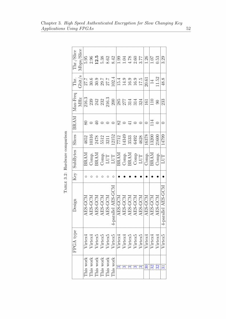
Chapter 3. High Speed Authenticated Encryption for Slow Changing KeyApplications Using FPGAs 52
Table3.2:
Har
dw
are
com
par
ison
FP
GA
typ
eD
esig
nK
eySubB
yte
sSlice
sB
RA
MM
ax-F
req
Thr.
Thr.
/Slice
MH
zG
bit
/sM
bps/
Slice
This
wor
kV
irte
x4
AE
S-G
CM
◦B
RA
M46
5280
216.
327
.75.
95T
his
wor
kV
irte
x4
AE
S-G
CM
◦C
omp.
1031
60
239
30.6
2.96
This
wor
kV
irte
x5
AE
S-G
CM
◦B
RA
M24
7840
242
30.9
12.5
This
wor
kV
irte
x5
AE
S-G
CM
◦C
omp.
5512
023
229
.75.
38T
his
wor
kV
irte
x5
AE
S-G
CM
◦L
UT
3211
021
6.3
27.7
8.62
This
wor
kV
irte
x5
4-par
alle
lA
ES-G
CM
◦L
UT
1215
20
200
102.
48.
42[3
]V
irte
x4
AE
S-G
CM
•B
RA
M77
1282
285
15.4
1.99
[3]
Vir
tex4
AE
S-G
CM
•C
omp.
1434
90
277
14.9
1.04
[3]
Vir
tex5
AE
S-G
CM
•B
RA
M35
3341
314
16.9
4.78
[3]
Vir
tex5
AE
S-G
CM
•C
omp
6492
031
416
.92.
60[3
]V
irte
x5
AE
S-G
CM
•L
UT
4628
032
417
.53.
77[3
0]V
irte
x4
AE
S-G
CM
•C
omp.
1637
80
161
20.6
11.
26[3
2]V
irte
x4
AE
S-G
CM
•B
RA
M13
200
114
110
141.
07[3
2]V
irte
x4
AE
S-G
CM
•C
omp.
2160
00
9011
.52
0.53
[31]
Vir
tex5
4-par
alle
lA
ES-G
CM
•L
UT
1479
90
233
48.8
3.29

Chapter 3. High Speed Authenticated Encryption for Slow Changing KeyApplications Using FPGAs 53
Ours(BRAM)
Ours(Comp)
[3](BRAM)
[3](Comp)
[30](Comp)
[32](BRAM)
[32](Comp)
[32](LUT)
5
10
15
20
25
30C
onsu
med
area
No. of slices (Kslice)No. of BRAMs (BRAMs/100)
Ours(BRAM)
Ours(Comp)
[3](BRAM)
[3](Comp)
[30](Comp)
[32](BRAM)
[32](Comp)
[32](LUT)
10
15
20
25
30
27.7
30.6
15.4 14.9
20.6
14
11.5
15.4
Sp
eed
per
form
ance
(Gbps)
Figure 3.9: Hardware comparison on Virtex4
proposed 4-parallel AES-GCM using pipelined KOA. Their design achieved
the authentication of 18 frames of 128-bits in 11 clock cycles because of the
latency resulting from the pipelined KOA. As a result, their throughput is
calculated as follows (highlighted before in Chapter 2):
Throughput(Mbps) = Fmax(MHz) × 128× 18
11. (3.6)
Fig. 3.9 presents the comparison between our proposed architectures and
previous work on Virtex-4. It is clear that our work outperforms the previously
reported ones. Therefore, proposed architectures can be used efficiently for
slow changing key applications like VPNs and embedded memory protection.

Chapter 3. High Speed Authenticated Encryption for Slow Changing KeyApplications Using FPGAs 54
3.5 Conclusion
In this chapter, we presented the performance improvement of AES-GCM by
key-synthesized method. We integrated this concept using three methods of
SubBytes implementation in order to increase the flexibility of the presented
work. With our proposed parallel AES-GCM, each multiplier has a fixed
operand. Therefore, the presented parallel AES-GCM is suitable for key-
synthesized method with higher throughput compared to the previous work.
The bitstream of the proposed architectures contains information related to
the used key. Hence, we presented a protocol to protect the bitstream of
the proposed architectures. Our presented AES-GCM architectures can be
used for slow changing key applications like VPNs and they outperform the
previous architectures regarding the hardware performance.

Chapter 4
Efficient and High Speed
Key-Independent AES-Based
Authenticated Encryption
Architectures Using FPGAs
4.1 Introduction
AES-GCM has been utilized in various security applications as a solution for
achieving both confidentiality and integrity. As we described before, it consists
of two components: an AES engine and a GHASH core. The performance of
the system is always determined by the GHASH architecture because of the
inherent computation feedback.
The previous chapter invested the slow changing key applications like VPNs
in order to design efficient and high speed architectures of AES-GCM by syn-
thesizing the used key for encryption and authentication into the architecture
(single and parallel). A new reconfiguration is loaded on the FPGA in case
of changing the key. However, this solution presented in Chapter 3 is only for
slow changing key applications.
55

Chapter 4. Efficient and High Speed Key-Independent AES-BasedAuthenticated Encryption Architectures Using FPGAs 56
By mid-December 2017, CAESAR, which is funded by NIST, will define a
portfolio of AE algorithms that offer advantages over AES-GCM. The due date
of the first-round submission for CAESAR was January 15th, 2014. AEGIS
is considered one of the candidates to the first round. First, it was presented
in SAC-2013 (Selected Area of Cryptography) and then becomes one of the
candidates of CAESAR.
In this chapter we are involved in designing high speed architectures of AES-
GCM in order to overcome the current challenges regarding the GHASH ar-
chitecture. Also, we focus on the hardware implementation of AEGIS-128.
The contributions of this chapter are as follows:
1. This chapter introduces an efficient method for implementing the pipelined
Karatsuba Ofman Algorithm (KOA)-based GHASH on FPGAs to sup-
port high speed applications. In particular, the computation feedback
is removed by analyzing the complexity of the computation process.
2. The proposed GHASH core is evaluated with three different implemen-
tations of AES ( BRAMs-based SubBytes, composite field-based Sub-
Bytes, and LUT-based SubBytes) in order to perform the encryption
and the authentication.
3. Because of being involved in designing high speed AE architectures,
an efficient AEGIS-128 architecture is presented using only five AES
rounds.
4.2 Efficient KOA-Based GHASH
Four different architectures of FPGAs-based AES-GCM were presented in
the open literature ([32],[30],[3],[31]). It is clear that these contributions
do generally have a common challenge related to the hardware performance
(Thr./Slice) as follows:
• In [32], the authors used the parallel method for implementing the
GHASH (GF (2128)) and the hardware performance is not sufficient to
support high speed applications because of using the parallel method.

Chapter 4. Efficient and High Speed Key-Independent AES-BasedAuthenticated Encryption Architectures Using FPGAs 57
• Because of the poor results of the hardware performance, the authors of
[30] proposed using KOA-based GHASH in order to reduce the hardware
complexity and improve the overall performance and their throughput
was as follows:
Throughput(Mbps) = Fmax(MHz) × 128. (4.1)
• For better throughput, [3] claimed the throughput improvement to their
previous KOA-based GHASH by using the pipelining concept (described
before in detail (see Equation 4.2)).
Throughput(Mbps) = Fmax(MHz) × 128× 8
19(4.2)
• The same happened with the parallel architecture proposed by [31] (see
Equation 4.3).
Throughput(Mbps) = Fmax(MHz) × 128× 18
11(4.3)
Also, in our previous architectures in Chapter 3, all the presented architectures
were key-dependent architectures because they are only for slow changing key
applications.
In this section, in order to improve the performance of AES-GCM, an efficient
pipelined KOA-based GHASH is presented to obtain key-independent AES-
GCM. The target is to present an efficient method that solves the problems
of the previous work.
In order to reduce the complexity (consumed area), KOA is selected to per-
form the multiplication process in the GHASH. In terms of the throughput
challenge, we present a new method to obtain a feedback-free multiplier. As
the targeted platform is FPGA, FPGA-specific properties are considered for
performance improvement.
In order to solve the problem of the inherent computation feedback in the
multiplier, we have to first analyze the processing equation of the GHASH
(Equation 4.4).

Chapter 4. Efficient and High Speed Key-Independent AES-BasedAuthenticated Encryption Architectures Using FPGAs 58
Output(Zi) = (Ci ⊕ Zi−1)×H (4.4)
As shown in Equation 4.4, the generation of the GHASH output is calculated
by the multiplication between H and the result of XORing the input Ci and
the previous output Zi−1. We propose writing Equation 4.4 as follows:
Output = (Ci ⊕ Zi−1)×H
= (Ci ×H)⊕ (Zi−1 ×H)
= (Ci ×H)⊕ [(Ci−1 ⊕ Zi−2)×H2]
= (Ci ×H)⊕ (Ci−1 ×H2)⊕ [(Ci−2 ⊕ Zi−3)×H3]
= (Ci ×H)⊕ (Ci−1 ×H2)⊕ (Ci−2 ×H3)
⊕[(Ci−3 ⊕ Zi−4)×H4]
= ((Ci ×H)︸ ︷︷ ︸⊕ (Ci−1 ×H2)︸ ︷︷ ︸⊕ (Ci−2 ×H3)︸ ︷︷ ︸⊕ (Ci−3 ×H4)︸ ︷︷ ︸ ....⊕ (C2 ×H i−1)︸ ︷︷ ︸⊕ (C1 ×H i)︸ ︷︷ ︸ .
(4.5)
According to Equation 4.5, the feedback resulting from XORing the input
Ci and the previous output Zi−1 could be removed because the final output
is calculated from the last two lines of the equation. More precisely, if the
values from H to H i exist, the feedback which affects the performance of the
multiplier will be removed.
Assume that there is a packet of data which contains 64 frames of 128-bit
(i=64, 1024 bytes) and the generation of the output (MAC) is required. There-
fore, Equation 4.5 will be as follows:
Output = ((C64 ×H)︸ ︷︷ ︸⊕ (C63 ×H2)︸ ︷︷ ︸⊕ (C62 ×H3)︸ ︷︷ ︸⊕ (C61 ×H4)︸ ︷︷ ︸ ....⊕ (C2 ×H63)︸ ︷︷ ︸⊕ (C1 ×H64).︸ ︷︷ ︸ (4.6)
If the values form H to H64 are stored and multiplied to the input Ci as
shown in Equation 4.6, the pipelined architecture can be simply performed.
The architecture proposed for the pipelined KOA-based GHASH is shown
in Fig. 4.1. The architecture shown in Fig. 4.1 is presented according to
calculating the output (MAC) of 64 frames of 128-bit. For area reduction,

Chapter 4. Efficient and High Speed Key-Independent AES-BasedAuthenticated Encryption Architectures Using FPGAs 59
Up/Down Counter
2nd
(64 to 32)
2nd
(64 to 32)
2nd
(64 to 32)
splittingstage
splittingstage
splittingstage
Sub−multstage
Sub−multSub−multstagestage
Alignment2
stageAlignment
stageAlignment
stage
22nd nd nd
stageAlignment1st
1 st
mod (P)
Z
Mux2Mux1
XY
Memory
H
H
2
64
Splitting stage (128 to 64)
H
Ad
dre
ss
Ci
Output
128
128
128128
128
128
128
128
6
255
128
Figure 4.1: Proposed pipelined KOA-based GHASH
we propose using 2-step KOA. The two 128-bit inputs (Ci and H) are split
two times in order to use 32-bit multipliers. Each sub-mult stage has three
32-bit multipliers. As a result, the complexity of the multiplier is reduced.
Additionally, Pipelining approach is used for reducing the datapath of the
multiplier. In total, the proposed architecture combines the following parts:

Chapter 4. Efficient and High Speed Key-Independent AES-BasedAuthenticated Encryption Architectures Using FPGAs 60
• 2-step pipelined KOA for performing the GF multiplication.
• A memory for storing the values from H2 to H64.
• 6-bit Up/Down counter for addressing the memory.
• Mux1 and Mux2 are used for switching between H, ci, Z, and the mem-
ory output.
We divide the process of the output (MAC) generation into two steps:
1. Initialization stage:
The first step includes storing the H values in the memory. At the
beginning, H is passed to X and Y ports. The counter counts up and
H2 will appear on port Z after 4 clock cycles because we use 4-stage
pipelined KOA. After, the memory stores H2 and H2 is passed to port
Y and H to port X in order to generate H3 and store it in the memory.
This process is repeated till filling the memory with the values from H2
to H64. Filling the memory takes 63 × 4 = 252 clock cycles. This is
called the initialization stage.
2. Output generation:
After initializing the memory, the second step concerns with the output
generation as presented in Equation 4.6. The counter starts counting
down with the first input. The first input C1 is passed to port Y and
the memory passes H64 to port X. After one clock cycle, the second
input C2 is passed to port Y and the memory passes H63 to port X.
This scenario is completed by passing C64 to port Y and H to port
X. The output is calculated by XORing Z values (Equation 4.6). In
terms of the time taken to generate the output, it is 64 clock cycles
with 5 additional clock cycles as a latency (4 clock cycles because of
the 4-stage pipelined KOA and one cycle because of the last register).
Therefore, the throughput of the proposed architecture is as follows:
Throughput(Mbps) = Fmax(MHz) × 128× 64
69. (4.7)

Chapter 4. Efficient and High Speed Key-Independent AES-BasedAuthenticated Encryption Architectures Using FPGAs 61
Because of targeting our architecture on Xilinx Virtex-5 FPGAs, we recom-
mend using CLBs for memory implementation because of 6-input Look-Up-
Tables (LUT). Otherwise, using BRAMs is another solution.
The proposed architecture offers the following advantages over the previous
designs:
• It reduces the reduction factor compared to [3] from 819
to 6469
(see Equa-
tion 4.7). Therefore, the developed architecture presents the throughput
improvement compared to [3].
• In case of changing the key, 252 clock cycles are needed to initialize the
memory. Hence, no new reconfiguration is needed in case of changing
the key unlike our previous architectures in Chapter 3.
4.3 High speed AES-GCM
This section describes adding the proposed GHASH to the pipelined AES in
order to perform the encryption and the authentication of the input message.
Fig. 4.2 shows the proposed high throughput architecture for AES-GCM. In
contrast to the previously presented AES-GCM architectures in Chapter 3, we
use the key-independent pipelined AES core which has the key schedule that
generates the sub-keys (k0 to k10) during the running time (no new FPGA
reconfiguration). Three SubBytes implementations (BRAMs-based SubBytes,
composite field-based SubBytes, and LUT-based SubBytes) are used in order
to increase the flexibility of the proposed architecture.
The proposed core performs both encryption and authentication as follows:
1. The pipelined AES engine generates H by encrypting ”00..00” frame.
2. The first value of the counter CTR[0] is encrypted.
3. The proposed GHASH needs 252 clock cycles in order to initialize the
memory after the generation of H.

Chapter 4. Efficient and High Speed Key-Independent AES-BasedAuthenticated Encryption Architectures Using FPGAs 62
Add Round Key
Round 1
Round 2
Round 10
Key
sch
edule
Pla
inte
xt
H
Cip
her
text(
C)
H
MA
C
CT
R
00..000
Key
Encr
ypti
on
Auth
enti
cati
on
KO
A−
bas
ed
E(C
TR
[0])
E(C
TR
[0])
Pro
pose
d
GH
AS
H
k0
k1
k2
k10
Figure4.2:
Pro
pos
edA
ES
-GC
Mar
chit
ectu
re

Chapter 4. Efficient and High Speed Key-Independent AES-BasedAuthenticated Encryption Architectures Using FPGAs 63
4. The AES engine changes its mode to be in CTR mode for performing
encryption and delivering Ci to the proposed GHASH.
5. The last value resulting from the proposed GHASH is XORed with
E(CTR[0]) in order to achieve the final MAC.
The presented architecture of AES-GCM perfectly suits the needs of GCM
mode which performs the encryption and the authentication of the input
message. As we described before, the encryption and the authentication in
GCM are performed using the pipelined AES in CTR mode and the pro-
posed GHASH, respectively. Therefore, the proposed architecture could also
be tuned to handle the decryption and the authentication. Indeed, Ci is
XORed with the output of the pipelined AES for performing the decryption
and also is passed to the proposed GHASH for MAC generation.
4.4 Efficient hardware implementation for AEGIS-
128
The goal of this section is to present our efficient and high speed architecture
of AEGIS-128. As shown in Equations 4.8, 4.9, and 4.10, encryption, au-
thentication and decryption tasks are performed by the five values of S (from
Si,0 to Si,4). In case of using one AES-round, the values from Si,0 to Si,4 are
updated every five clock cycles.
Ci = Pi ⊕ Si,1 ⊕ Si,4 ⊕ (Si,2&Si,3) (4.8)
MAC = ⊕4i=0(S(msglen
128+7),i) (4.9)
Pi = Ci ⊕ Si,1 ⊕ Si,4 ⊕ (Si,2&Si,3) (4.10)
In our proposed architecture shown in Fig. 4.3, five AES-rounds are used in
order to generate the values from Si+1,0 to Si+1,4 in one clock cycle. In terms

Chapter 4. Efficient and High Speed Key-Independent AES-BasedAuthenticated Encryption Architectures Using FPGAs 64
of the hardware implementation, 80 s-boxes and 20 Mixcolumns are used.
SubBytes stage is implemented by using LUT and composite field methods
because using BRAMs adds a register (see Fig. 3.2) which is not be suitable
with the iterative nature of AEGIS. Multiplexers from M1 to M5 are used to
switch between the initialization mode to the encryption and the finalization
modes. M6 is to support mi to the state update function where:
mi =
K128 Initialization(i = even)
K128 ⊕ IV128 Initialization(i = odd)
P Encryption
Smsglen128
,3 ⊕ tmp Finalization.
1. The initialization of AEGIS-128:
As we described before, the initialization of AEGIS-128 consists of load-
ing the key and IV into the state in 10 steps (i=-10 to -1). The initial-
ization stage is performed as follows:
• The used multiplexers (M1 to M5) pass the values Sinit,0, Sinit,1,
Sinit,2, Sinit,3, and Sinit,4 to the five AES-rounds during the first
step.
• During the next 9 steps, the values Si+1,0, Si+1,1, Si+1,2, Si+1,3, Si+1,4
are fed to the multiplexers (M1 to M5). Also, M6 passes the values
m2i = K128 or m2i+1 = K128 ⊕ IV128 according to the step number
(even or odd). This takes 10 clock cycles as an initialization stage.
2. The encryption of AEGIS-128:
After completing the initialization stage, the encryption is performed as
shown in Equation 4.8 when M6 passes the plaintext (P) to be mixed
with Si,0. Encrypting 128-bit input takes only one clock cycle because
of using five AES-rounds.
3. The finalization of AEGIS-128:
After processing all the input message encryption, the finalization starts

Chapter 4. Efficient and High Speed Key-Independent AES-BasedAuthenticated Encryption Architectures Using FPGAs 65
msg
len
128
,3
SS
SS
Sin
it,0
init
,1in
it,2
init
,3in
it,4
SS
SS
i+1,1
i+1,2
i+1,3
i+1,4
SS
SS
Si,
0i,
1i,
2i,
3i,
4
Si+
1,0
SS
SS
SS
i+1,1
i+1,3
Si+
1,4
Cip
her
tex
t (C
)T
ag
Si+
1,0
Si+
1,2
2i
m
2i+
1m
i+1,1
i+1,4
i+1,2
i+1,3
P
S
M1
M2
M3
M4
M5
M6
AE
S R
ou
nd
AE
S R
ou
nd
AE
S R
ou
nd
AE
S R
ou
nd
AE
S R
ou
nd
Figure4.3:
Pro
pos
edh
igh
spee
dA
EG
IS-1
28ar
chit
ectu
re

Chapter 4. Efficient and High Speed Key-Independent AES-BasedAuthenticated Encryption Architectures Using FPGAs 66
in order to achieve the authentication task. M6 passes the value Smsglen128
,3⊕tmp. This starts from i= (msglen
128) to (msglen
128+ 6). As a result, the final-
ization stage takes 6 clock cycles.
It is clear that any process of AEGIS-128 (encryption, decryption, or authen-
tication) depends on the generation of the values from Si+1,0 to Si+1,4 which
takes only one clock cycle. Hence, the overall throughput is calculated as
follows:
Throughput(Mbps) = Fmax(MHz) × 128 (4.11)
The proposed architecture of AEGIS-128 could also be tuned to handle the
decryption and the authentication by processing Ci into Equation 4.10 for per-
forming the decryption and there is no change in terms of the authentication
stage.
4.5 Hardware comparison
We coded our proposed schemes in VHDL and targeted to Virtex-5 (XC5VLX220).
ModelSim 6.5c was used for simulation. Xilinx Synthesize Technology (XST)
is used to perform the synthesize and ISE9.2 was adopted to run the Place
And Route (PAR).
Table 4.1 shows the hardware comparison between our results and
previous work. Note the filled dots in the ”Key” column. The
key is synthesized into the architecture when denoted by ◦ which
requires a new reconfiguration in case of changing the key. Other-
wise, the key schedule is implemented when denoted by • and no
new reconfiguration is needed in case of changing the key.
On Virtex-5 platform, our proposed AES-GCM core reaches the throughput of
32.46 Gbps with the area consumption of 3836 slices and 50 BRAMs. In case of
using composite field SubBytes, it consumes 7475 slices, however no BRAMs
are required. In terms of using LUT SubBytes, the proposed architecture

Chapter 4. Efficient and High Speed Key-Independent AES-BasedAuthenticated Encryption Architectures Using FPGAs 67
Table4.1:
Har
dw
are
com
par
ison
FP
GA
Des
ign
key
SubB
yte
sSlice
sB
RA
Ms
Max
-Fre
qT
hr.
Thr.
/Slice
MH
zG
bit
/sM
bps/
Slice
This
wor
kV
irte
x5
AE
S-G
CM
•B
RA
M38
3650
273.
432
.46
8.4
6T
his
wor
kV
irte
x5
AE
S-G
CM
•C
omp.
7475
026
4.2
31.3
64.1
9T
his
wor
kV
irte
x5
AE
S-G
CM
•L
UT
4770
031
136
.92
7.7
4T
his
wor
kV
irte
x5
AE
GIS
-128
•C
omp.
2729
084
.910
.87
3.98
This
wor
kV
irte
x5
AE
GIS
-128
•L
UT
1391
015
6.5
20.0
314
.39
[3]
Vir
tex5
AE
S-G
CM
•B
RA
M35
3341
314
16.9
4.78
[3]
Vir
tex5
AE
S-G
CM
•C
omp
6492
031
416
.92.
60[3
]V
irte
x5
AE
S-G
CM
•L
UT
4628
032
417
.53.
77[3
1]V
irte
x5
AE
S-G
CM
•B
RA
M95
6145
023
348
.85.
1[3
1]V
irte
x5
AE
S-G
CM
•C
omp
1850
50
233
48.8
2.64
[31]
Vir
tex5
AE
S-G
CM
•L
UT
1479
90
233
48.8
3.29
This
wor
k(C
hap
ter
3)V
irte
x5
AE
S-G
CM
◦B
RA
M24
7840
242
30.9
12.5
This
wor
k(C
hap
ter
3)V
irte
x5
AE
S-G
CM
◦C
omp.
5512
023
229
.75.
38T
his
wor
k(C
hap
ter
3)V
irte
x5
AE
S-G
CM
◦L
UT
3211
021
6.3
27.7
8.62

Chapter 4. Efficient and High Speed Key-Independent AES-BasedAuthenticated Encryption Architectures Using FPGAs 68
occupies 4770 and reaches the throughput of 36.92 Gbps. Also, by using using
LUT, our presented AEGIS-128 architecture consumes 1391 and reaches the
throughput of 20.03 Gbps. Regarding composite field, it consumes 2729 with
10.87 Gbps as a throughput.
By comparing our results of AES-GCM to [3], the comparison shows that our
performance (Thr./Slice) is better. This improvement results from reducing
the reduction factor in the equation of throughput as shown in Equation 4.2
and Equation 4.7. Also, our presented AEGIS-128 architectures performance
is better than [3].
In terms of the 4-parallel AES-GCM by [31], our area consumption of AES-
GCM and AEGIS-128 is smaller compared to them. Also, our performance
is better because the throughput presented by [31] is calculated as shown in
Equation 4.3.
Our previous chapter presented architectures for slow changing key applica-
tions like VPNs and the FPGA needs a new reconfiguration when the key
changes. Therefore, the proposed architectures in this chapter present bet-
ter performance compared to our previous AES-GCM (Chapter 3) because
the FPGA does not need a new reconfiguration when the key changes but it
needs 252 clock cycles for the memory initialization or 10 clock cycles in case
of AES-GCM and AEGIS-128, respectively.
We believe that the design presented by [3] is the closest one to our specifi-
cations, performance goals, technology and methodology. It is not a parallel
design like [31]. Also, it supports the key variation without any new recon-
figuration unlike our previous architectures in Chapter 3. Therefore, Fig 4.4
shows the overall comparison between our architectures and [3]. In terms
of the consumed area, our designs are slightly more than [3]. However, It
clear that the presented throughput is better than [3]. In general, the overall
performance of our architectures is always better than [3].

Chapter 4. Efficient and High Speed Key-Independent AES-BasedAuthenticated Encryption Architectures Using FPGAs 69
Ours(BRAM)
Ours(Comp)
Ours(LUT)
[3](BRAM)
[3](Comp)
[3](LUT)
4
5
6
7
Con
sum
edar
ea
No. of slices (Kslice)No. of BRAMs (BRAMs/100)
Ours(BRAM)
Ours(Comp)
Ours(LUT)
[3](BRAM)
[3](Comp)
[3](LUT)
15
20
25
30
35
32.6431.36
36.92
16.9 16.9 17.5Sp
eed
per
form
ance
(Gbps)
Ours(BRAM)
Ours(Comp)
Ours(LUT)
[3](BRAM)
[3](Comp)
[3](LUT)
4
6
88.46
4.19
7.74
4.78
2.6
3.77
Har
dw
are
per
form
ance
(Thr.
/Slice
)
Figure 4.4: Hardware comparison on Virtex-5

Chapter 4. Efficient and High Speed Key-Independent AES-BasedAuthenticated Encryption Architectures Using FPGAs 70
4.6 Conclusion
In this chapter, we presented the performance improvement of AES-GCM
(Thr./Slice). This was achieved by proposing an efficient pipelined KOA-
based GHASH. With our proposed GHASH, the throughput reduction factor
is decreased because of the feedback-free design. The presented multiplier
was evaluated with three different AES implementations (BRAMs-based Sub-
Bytes, composite field-based SubBytes, and LUT-based SubBytes) in order to
increase the flexibility of the presented AES-GCM. Furthermore, we designed
an efficient architecture for AEGIS-128 which is considered one of the candi-
dates of CAESAR by only five AES rounds with better performance compared
to the previous work. The throughput of the presented cores ranges from 10.87
to 36.92 using Xilinx Virtex-5 FPGAs. It is shown that the performance of
the presented architectures outperforms the previously reported ones.

Part II
Low Cost Solutions for Secure
FPGA Reconfiguration
71

Chapter 5
Low Cost Solutions for Secure
FPGA Reconfiguration
5.1 Introduction
When FPGAs were first introduced in the 1980s, this was a revolutionary step
from static ASIC and VLSI solutions to flexible and maintainable hardware
applications. With FPAGs, it has become possible to avoid the static designs
of standard VLSI technology, and instead to compile electrical circuits for
arbitrary hardware functions into configuration bitstreams which are used to
program a fabric of reconfigurable logic.
Designing using FPGAs allows faster design cycles than ASICs because they
enabled early functionality testing. Therefore, the use of FPGAs has been
expanding from its traditional role in prototyping to mainstream production.
The reconfiguration of FPGAs includes downloading the bitstream file which
contains the new design on the FPGA. Reconfiguration of FPGAs is becoming
increasingly popular particularly in networking applications. The option to
reconfigure the FPGAs dynamically opens up the threat of stealing the Intel-
lectual Property (IP) of the design. Since the configuration is usually stored in
external memory, this can be easily tapped and read out by an eavesdropper.
72

Chapter 5. Low Cost Solutions for Secure FPGA Reconfiguration 73
The main goals and achievements of this chapter are as follows:
1. Giving an overview of security issues used in the reconfiguration of FP-
GAs.
2. Analyzing how well encryption and authentication are very important
for trusted designs on FPGAs.
3. Proposing low cost hardware implementations to support and authenti-
cate the encrypted bitstreams.
5.2 FPGA reconfiguration
Programmability manages the user to modify the functionality of a device
outside of the founder. By applying this concept on gate arrays gives us Field
programmable Gate Arrays (FPGAs). As we described before, the function-
ality of the FPGA is modified when the new bitstream is uploaded into the
FPGA. The static part processes the bitstream and delivers it to the SRAM
cells which reload the reconfigurable part with the new design.
Networked FPGA-based systems gain particular flexibility if remote reconfig-
uration updates are possible. It is attractive as it is used in such systems to
offer new multimedia features or to repair eventual security issues remotely. It
requires transmitting the bitstream file which contains the hardware IP from
the development location over public (insecure) channels and thus introduces
new security issues (see Fig. 5.1) .
The developer is faced with several problems resulting from sending the bit-
stream file through insecure network. An adversary attacker can detect the
hardware IP to sell illegal copies or leak it to the public domain. There are
several types of attacks could be occurred to the bitstream file:

Chapter 5. Low Cost Solutions for Secure FPGA Reconfiguration 74
Application
FPGA
User Logic
SR
AM
Mem
ory
C
ells
Static Part
Public Network
Bitstream
Bitstream
Development
Location
Bitstream
Non Volatile
Memory (NVM)
Figure 5.1: Remote reconfiguration
1. Cloning attack:
The bitstream generated for one FPGA can be implemented on other of
the same family and size. Therefore, attackers can clone the bitstream
by copying it during sending it to the FPGA in order to sell the IP
illegally (see Fig. 5.2).
Bitsream Extract copy
010110010
110100100
010101010
010110010
111010100
110100100
010101010
111010100
Figure 5.2: Cloning attack

Chapter 5. Low Cost Solutions for Secure FPGA Reconfiguration 75
2. Reverse engineering attack:
It is the transformation of an encoded bistream into a logical functional
description which is equivalent to the original design as shown in Fig.
5.3. The attacker extracts data from the bitstream such as keys and
BRAMs content. An example of how the original design is recovered
from the bitstream is shown in [40].
Bitsream
010110010
111010100
110100100
010101010
Figure 5.3: Reverse engineering attack
3. Tampering attack:
In this type of attack, the attacker changes the design and sends it to
the FPGA (see Fig. 5.4). In [41], the authors presented how an FPGA
is damaged by malicious tampering of bitstreams.
11110
110100100
Tampered copyBitsream
010110010
111010100
110100100
010101010
1011001001011
101010101
Figure 5.4: Tampering attack
5.3 Previous work
This section describes the previous methods used to secure the bitstream file
during the reconfiguration process.

Chapter 5. Low Cost Solutions for Secure FPGA Reconfiguration 76
• Bitstream confidentiality:
Encrypting the bistream by the developer and decrypting it within the
FPGA protects against cloning and reverse engineering attacks. En-
crypting the reconfiguration of the programmable devices was first in-
troduced by [42]. Kean [2] proposed encrypting and decrypting the
bitstream using embedded keys (programmed by the FPGA developer).
Both encryption and decryption are performed within the FPGA itself.
As shown in Fig. 5.5, the first step is performed in a trusted facil-
ity where the bitstream is encrypted by the FPGA using its embedded
key K, and then stored in NVM. While the system is deployed in the
field, the bitstream is decrypted with the same embedded key using a
hard-core decryptor which is part of the static logic. The advantage of
this method is that the key is embedded in the static part and it never
leaves the FPGA. The disadvantage is that the need for a trusted envi-
ronment in case of encrypting a new bitstream. Also, both encryptors
and decryptors must be used because the authors used AES-128 in CBC
mode, prohibitive cost. In [43], the authors proposed using the partial
reconfiguration to encrypt and decrypt the bitsream. This means that
the encryption and decryption circuits leave the static logic to be in the
user logic. As a result, the static area is free. However, the key used for
encryption and decryption is accessible to the user logic, where any one
can read it out and decrypt the bitstream.
Current FPGAs include hardwired mechanisms that ensure bitstream
confidentiality [44]. Bitstream encryption, introduced by Xilinx on a
production level with Virtex II FPGAs to prevent device cloning and
to protect the confidentiality of the design data. Each Virtex-4, Virtex-
5, and Virtex-6 device have an on-chip advanced encryption standard
(AES) [45] decryption engine to support encrypted bitstreams.

Chapter 5. Low Cost Solutions for Secure FPGA Reconfiguration 77
User Logic
SR
AM
Mem
ory
C
ells
Static Part
FPGA
ApplicationHMAC
Non Volatile
Memory (NVM)
Encrypted bitstream
Encrypted Bitstream
ENC
DEC
K
K
User Logic
SR
AM
Mem
ory
C
ells
Static Part
FPGA
ApplicationHMAC
Non Volatile
Memory (NVM)
Encrypted bitstream
Encrypted Bitstream
ENC
DEC
K
K
HMACHMAC
User Logic
SR
AM
Mem
ory
C
ells
Static Part
FPGA
ApplicationHMAC
Non Volatile
Memory (NVM)
Encrypted bitstream
Encrypted Bitstream
ENC
DEC
K
K
User Logic
SR
AM
Mem
ory
C
ells
Static Part
FPGA
ApplicationHMAC
Non Volatile
Memory (NVM)
Encrypted bitstream
Encrypted Bitstream
ENC
DEC
K
K
Bitstream
Step 2
Step 1
Figure 5.5: Bitstream encryption/decryption by [2]
The Xilinx bitstream encryption system consists of two parts:
– Software-based bitstream encryption.
– On-chip bitstream decryption.

Chapter 5. Low Cost Solutions for Secure FPGA Reconfiguration 78
By using the Xilinx ISE software, the user generates both the encryp-
tion key and the encrypted bitstream. The encryption key can only
be programmed into the device via the JTAG port by the developer.
These devices store the encryption key internally in either dedicated
RAM, backed up by a small externally connected battery, or in one-
time-programmable (OTP) fuses.
After programming the FPGA with the key which is used for encryp-
tion and decryption, as outlined in Fig. 5.6, the bitstream is delivered
securely to the FPGA as follow:
1. The bitstream is encrypted by developer using the assigned key K.
2. The encrypted bitstream is sent to the NVM.
3. The NVM supports the FPGA with the encrypted bitstream in
order to be decrypted using the static logic which contains the
AES core.
4. The decrypted bitstream is passed to the SRAM cells to implement
the new design.
Although this mechanism allows for protection of the system designer’s
IP against cloning as well as reverse engineering, it does not ensure the
authenticity of the bitstream. Therefore, this solution is not enough
to prevent attackers from destroying the FPGA using certain malicious
bitstreams. As a result, the FPGA should accept only bitstreams from
an authenticated source.
• Bitstream integrity:
Tampering attack is based on the modification of the bitstream. The
authors of [41] showed the effect of malicious tampering of bitstreams.
They presented how an FPGA is damaged due to shorts caused by ma-
nipulating configuration bits that control pass gates. Therefore, the
FPGA must be smart enough to detect the concept of Who is the
sender?, to accept the correct bitstream sent by the trusted sender.
Some FPGA vendors implement Cyclic Redundancy Checks (CRC) [46].
However, the purpose of CRC is to detect transmission errors, not to
check the integrity of data in the cryptographic sense. This is why Xilinx

Chapter 5. Low Cost Solutions for Secure FPGA Reconfiguration 79
User Logic
SR
AM
Mem
ory
C
ells
Static Part
FPGA
AES Application
KEncrypted Bitstream
Non Volatile
Memory (NVM)
Bitstream
K
AES
Encrypted Bitstream
Figure 5.6: Bitstream encryption
[47] suggested using Message Authentication Code (MAC) function to
ensure the integrity of the bitstream. Virtex-6 FPGAs are an example of
the programmable devices that offer cryptographically strong bitstream
authentication.
An on-chip bitstream keyed-MAC algorithm implemented in hardware
provides additional security beyond that of using AES bitstream encryp-
tion alone [47]. Without knowledge of the AES and HMAC keys, the
bitstream cannot be loaded, modified, or cloned.
As shown in Fig. 5.7, the developer sends the bitstream securely to the
FPGA as follows:
1. The developer processes the bitstream via the AES and HMAC
using k1 and k2 respectively in order to encrypt and authenticate
the bitstream.
2. The encrypted bitsream and the MAC are sento to the NVM.

Chapter 5. Low Cost Solutions for Secure FPGA Reconfiguration 80
User Logic
SR
AM
Mem
ory
C
ells
Static Part
FPGA
Application
AES
k2K1
Match?
bitstream
MAC
Encrypted
Y/N
HMAC
Developer
Bitstream
HMACAES
Encrypted Bitstream
MA
C
k2K1
Encrypted Bitstream
MA
C
Memory (NVM)
Non Volatile
Figure 5.7: Bitstream encryption and authentication in Virtex6
3. The NVM is used to store the encrypted bitstream with its MAC
and send them to the FPGA.
4. The FPGA static part is responsible for decrypting and authenti-
cating the contents of the NVM.
5. The computed MAC is compared to the bitstream’s MAC. If they
are equal, the FPGA will continue to the start-up sequence. Oth-
erwise, configuration will abort and the cells be cleared.
Drimer [48] proposed an FPGA bitstream encryption-authentication
mechanism based on two parallel AES engines, in CTR and CBC modes,
for performing both encryption and authentication. His solution used
the architectures presented by Parelkar [25] who noted that generic com-
position of authentication and encryption (AES+HMAC) required more
circuit area than AE algorithms. Therefore, Parelkar [25] presented
CCM mode for achieving both authentication and encryption. Table
5.1 shows the difference between the hardware implementation of CCM
mode and AES+HMAC. It is clear that CCM needs smaller area than
AES combined with HMAC. In [49], the authors proposed using ALE

Chapter 5. Low Cost Solutions for Secure FPGA Reconfiguration 81
algorithm for performing both decryption and authentication but this
algorithm was attacked by [50, 51].
Table 5.1: Hardware comparison
Design architecture Technology Area Frequency Throughput
mm2 MHz Mbps
Parelkar et al.[25] AES-CCM 90 nm 0.057 148 434
Parelkar et al.[25] AES+HMAC 90 nm 0.183 101.2 1293
As mentioned above, most of the previous work used the static part in order
to perform only decryption or both decryption and authentication of the en-
crypted bitstream [2, 48, 52]. However, in order to leave the static part free for
the developed application, Bossuet et al. [43] used the user part to decrypt
the encrypted bitstream. Table 5.2 summarizes and compares between the
previous work.
Our presented approach in the following section utilizes the static part in order
to perform both decryption and authentication by an embedded key in the
static part. As a result, the used key will never leave the static part (more
secure). In order to reduce the area of the proposed solution in the static part,
low cost AE algorithms will be implemented.
5.4 Low cost AE architecture for secure re-
configuration
Our goal is to design low cost solutions to be used for decryption and authenti-
cation of the encrypted bitstream. The reason of the low cost implementation
is to reduce the used area of the static part which performs the security task.
The used key is always embedded in the static part to avoid any user access.
Efficient hardware implementations for AE are presented and compared with
previous work. Presented architectures include AES-CCM, AES-GCM, and
AEGIS-128 which can be used efficiently for secure reconfiguration of FPGAs.

Chapter 5. Low Cost Solutions for Secure FPGA Reconfiguration 82
Table5.2:
Pre
vio
us
wor
ksu
mm
ery
Des
ign
Bit
stre
amB
itst
ream
Key
acce
ssC
ore
exis
tence
Tru
sted
envir
onm
ent
Are
are
quir
emen
t
confiden
tial
ity
inte
grit
yst
orag
efo
rre
configu
rati
on
[2]
Yes
No
Sta
tic
par
tSta
tic
par
tY
esA
ES-b
ased
encr
ypto
ran
ddec
rypto
r
[43]
Yes
No
Use
rP
art
Use
rP
art
No
AE
S-b
ased
encr
ypto
ran
ddec
rypto
r[5
2]Y
esN
oSta
tic
par
tSta
tic
par
tN
oA
ES-b
ased
dec
rypto
r[4
7]Y
esY
esSta
tic
par
tSta
tic
par
tN
oA
ES-b
ased
dec
rypto
r+
HM
AC
[48]
Yes
Yes
Sta
tic
par
tSta
tic
par
tN
oA
ES-C
CM

Chapter 5. Low Cost Solutions for Secure FPGA Reconfiguration 83
The ASIC implementation is the main target, since the bitstream decryption
and authentication modules are meant to be implemented as an independent
IP in the static part (FPGA silicon).
User Logic
SR
AM
Mem
ory
C
ells
Static Part
Match?
Low Cost AE
Y/N
FPGA
Encrypted Bitstream
MAC
ComputedMAC
Key
Application
Encrypted Bitstream
MA
C
Non Volatile
Memory (NVM)
Bitstream
KeyAE
MA
C
Dev
eloper
Encrypted Bitstream
Figure 5.8: our Proposed approach
As shown in Fig. 5.8, the developer encrypt and authenticate the bitstream
using AE (AES-CCM, AES-GCM, or AEGIS-128). After, the encrypted bit-
sream and the MAC are sent to the NVM. The NVM sends the encrypted
bitstream with its MAC at the power-up. The low cost AE inserted in the
static part decrypts and verifies the MAC for performing the secure reconfig-
uration.
5.4.1 Proposed AES-CCM
In the implementation of our AES-CCM core, we have focused on minimizing
the area. Since AES-CCM uses two blocks of AES in CTR and CBC modes
for performing both encryption and authentication, the proposed architecture
uses only one AES block for both encryption/decryption and authentication
in order to obtain an area-efficient architecture.

Chapter 5. Low Cost Solutions for Secure FPGA Reconfiguration 84
In [48], the authors motivated using the presented AES-CCM proposed by
[25] in order to secure the reconfiguration process. In [25], one round-based
AES (iterative design) was used to implement AES-CCM. As a result, the
complexity of their design was sixteen SubBytes with four Mixcolumns.
+
MixColumns
32323232
32323232
Shift
key
128
Plaintext (P)
SSSS
32
32
32
32
32
32
128
128
128
128
8888
8888
3232323232
32323232
32
Key Schedule
Ciphertext (C)128
32323232
Figure 5.9: 1/4 round-based AES
In the proposed AES-CCM, we use 1/4 round-based AES that has an advan-
tage of reducing the consumed area with a suitable throughput which is able
to support applications lower than 1Gbps. Fig. 5.9 shows the architecture
of 1/4 round-based AES. The data path is reduced from 128-bit to 32-bit.
Hence, only four SubBytes (s-boxes) and one MixClolumn are used. The key
schedule shares the four s-boxes stage with the main data path to avoid using
another four s-boxes. Additionally, the SubBytes stage is implemented using
composite field for reducing the consumed area.

Chapter 5. Low Cost Solutions for Secure FPGA Reconfiguration 85
Each round processes the 128-bit frame in five clock cycles (four clock cycle
for the main frame + one clock cycle because the key schedule shares the
s-boxes with the main data path). Because of using AES-128, 10 rounds
must be computed to achieve the encryption/decryption process. In order to
encrypt/decrypt a 128-bit frame, 50 clock cycles are needed (5×10). Therefore
the throughput of the 1/4 round-based AES is as follows:
Throughput(Mbps) =Fmax(MHz) × 128
50. (5.1)
Our AES-CCM architecture uses one 1/4 round-based AES for both encryp-
tion and authentication as shown in Fig. 5.10. Encryption and authentication
are computed as follows:
+
+
Counter
Plaintext (P)
Memory
+
Key
128
128
128
128 1281/4 round−based
AES
Ciphertext (C)
Direction of encryption using CTR mode
Direction of authentication using CBC mode
128
128
Y
S[0]
MAC
Figure 5.10: Proposed AES-CCM (encryption and authentication)
1. The plaintext (P), which is stored in a memory (not online), is processed
by 1/4 round-based AES in CBC mode in order to generate Y.

Chapter 5. Low Cost Solutions for Secure FPGA Reconfiguration 86
2. CTR[0] is encrypted to achieve S[0] which is XORed with Y to generate
the MAC.
3. Encryption is then performed by 1/4 round-based AES in CTR mode.
The same architecture could be tuned to handle both decryption and authen-
tication as follows (see Fig. 5.11):
1. CTR[0] is encrypted to obtain S[0].
2. Decryption is computed by XORing the encrypted counter values with
the ciphertext (C) to obtain the plaintext (P).
3. The plaintext (P) is processed by 1/4 round-based AES in CBC mode
to perform the authentication by the generation of Y which is XORed
with S[0] to obtain the MAC.
+
+
Counter
Memory
Plaintext (P)
+Memory
Plaintext (P)
Key
128
128
128
128
128 1281/4 round−based
AES
Ciphertext (C)
Direction of decryption using CTR mode
Direction of authentication using CBC mode
Y
MAC
S[0]
128
Figure 5.11: Proposed AES-CCM (decryption and authentication)

Chapter 5. Low Cost Solutions for Secure FPGA Reconfiguration 87
Compared to the solution of [48], the proposed architecture consumes only four
s-boxes and one MixColumn instead of sixteen s-boxes and four MixColumns.
A 128-bit frame takes 50 clock cycles to be encrypted/decrypted or added to
MAC queue. Therefore, the achieved throughput of our presented AES-CCM
is calculated as follows:
Throughput(Mbps) =128× Fmax(MHz)
50× 2. (5.2)
5.4.2 Proposed AES-GCM
AES-GCM uses two components: an AES engine and a GF(2128) multiplier.
The target is directed to optimize the overall architecture which includes the
encryption/decryption part (AES) and the authentication part (GF(2128)).
Our proposed architecture uses the 1/4 round-based AES for area optimiza-
tion. Previous architectures of GF(2128) such as [30, 34] were used for high
speed applications. In terms of the hardware implementation, they are expen-
sive. Hence, it is important to design a multiplier which can be used efficiently
with the 1/4 round-based AES.
Serial GF(2128) multiplier is described in Algorithm 1 [12], where A,H are
inputs to the multiplier and F(x) is the field polynomial, F (x) = x128 + x7 +
x2 + x + 1. The output C needs 128 clock cycles to be ready in case of using
serial multiplier.
As shown in Algorithm 1, it is possible to design one round for achieving the
multiplication in 128 clock cycles. Four rounds are used together to reduce
the number of clock cycles needed to perform the multiplication from 128 to
32 (128/4) clock cycles in order to be suitable for the 1/4 round-based AES
architecture as shown in Fig. 5.12.
Our proposed AES-GCM architecture shown in Fig. 5.13 uses 1/4 round-
based AES with the hybrid GF(2128) multiplier to accomplish the task of
encryption and authentication. In case of performing both encryption and
authentication, the sequence is as follows:

Chapter 5. Low Cost Solutions for Secure FPGA Reconfiguration 88
(A)A = rightshift
+C C A
127
128Algorithm 1 : GF(2 ) Multiplier
Input A,H, F(x) Field Polynomial
For i=0 to 127 do
iIF H =1 Then
Output C
End IF
IF A = 0 Then
Else
+(A)A = rightshift
End If
F(x)
End For
Return C
One Round
AH
A1C1H1
A2C2H2
H3 C3 A3
A4C4H4
C="00..00"
C
Round
Round
Round
Round
Figure 5.12: Proposed GF(2128) multiplier

Chapter 5. Low Cost Solutions for Secure FPGA Reconfiguration 89
+
Counte
r
"00...0
00"
++
E (
CT
R[0
])
E (
CT
R[0
])
12
8
12
8
12
8
Hybri
d G
F
Mult
ipli
er
H
H
MA
C
Pla
inte
xt
(P)
Cip
her
text
(C)
12
8
12
8
12
8
12
8
12
81
28
12
8
1/4
Round−
bas
ed
AE
S
Figure5.13:
Pro
pos
edA
ES
-GC
M(e
ncr
yp
tion
and
auth
enti
cati
on)

Chapter 5. Low Cost Solutions for Secure FPGA Reconfiguration 90
1. ”00..00” frame is encrypted to obtain H.
2. CTR[0] is encrypted (it is used later for authentication).
3. Encryption is performed by 1/4 round-based AES in CTR mode.
4. Encrypted frames are passed to the hybrid multiplier for performing the
authentication.
The presented architecture could be also tuned for performing both decryption
and authentication as follows (see Fig. 5.14):
1. ”00..00” frame is encrypted to obtain H.
2. CTR[0] is encrypted (it is used later for authentication).
3. Decryption is computed by the 1/4 round-based AES in CTR mode,
where the ciphertext (C) is XORed with the encrypted counter values
to obtain the plaintext (P).
4. The ciphetext (C) is passed to the hybrid multiplier for performing the
authentication.
It is clear from Fig. 5.13 and Fig. 5.14 that each frame is encrypted/decrypted
in 50 clock cycles and added to MAC queue in 32 clock cycles for authentica-
tion. As a result, the throughput of the proposed AES-GCM is calculated as
follows:
Throughput(Mbps) =128× Fmax
50. (5.3)
The advantage of AES-GCM over AES-CCM is that AES-GCM supports on-
line applications because of the external hashing using the GF(2128). Hence,
there is no need for the memory to store the plaintext (P). Also, the through-
put is higher (see Equations 5.2 and 5.3).

Chapter 5. Low Cost Solutions for Secure FPGA Reconfiguration 91
+
Counte
r
"00...0
00"
++
E (
CT
R[0
])
E (
CT
R[0
])
12
8
12
8
12
8
Hybri
d G
F
Mult
ipli
er
H
H
MA
C
12
8
12
8
12
8
12
81
28
12
8
1/4
Round−
bas
ed
AE
S
Cip
her
text
(C)
Pla
inte
xt
(P)
Cip
her
text
(C)
Figure5.14:
Pro
pos
edA
ES
-GC
M(d
ecry
pti
onan
dau
then
tica
tion
)
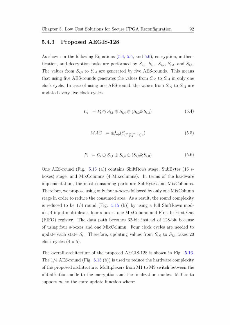
Chapter 5. Low Cost Solutions for Secure FPGA Reconfiguration 92
5.4.3 Proposed AEGIS-128
As shown in the following Equations (5.4, 5.5, and 5.6), encryption, authen-
tication, and decryption tasks are performed by Si,0, Si,1, Si,2, Si,3, and Si,4.
The values from Si,0 to Si,4 are generated by five AES-rounds. This means
that using five AES-rounds generates the values from Si,0 to Si,4 in only one
clock cycle. In case of using one AES-round, the values from Si,0 to Si,4 are
updated every five clock cycles.
Ci = Pi ⊕ Si,1 ⊕ Si,4 ⊕ (Si,2&Si,3) (5.4)
MAC = ⊕4i=0(S(msglen
128+7),i) (5.5)
Pi = Ci ⊕ Si,1 ⊕ Si,4 ⊕ (Si,2&Si,3) (5.6)
One AES-round (Fig. 5.15 (a)) contains ShiftRows stage, SubBytes (16 s-
boxes) stage, and MixColumns (4 Mixcolumns). In terms of the hardware
implementation, the most consuming parts are SubBytes and MixColumns.
Therefore, we propose using only four s-boxes followed by only one MixColumn
stage in order to reduce the consumed area. As a result, the round complexity
is reduced to be 1/4 round (Fig. 5.15 (b)) by using a full ShiftRows mod-
ule, 4-input multiplexer, four s-boxes, one MixColumn and First-In-First-Out
(FIFO) register. The data path becomes 32-bit instead of 128-bit because
of using four s-boxes and one MixColumn. Four clock cycles are needed to
update each state Si. Therefore, updating values from Si,0 to Si,4 takes 20
clock cycles (4× 5).
The overall architecture of the proposed AEGIS-128 is shown in Fig. 5.16.
The 1/4 AES-round (Fig. 5.15 (b)) is used to reduce the hardware complexity
of the proposed architecture. Multiplexers from M1 to M9 switch between the
initialization mode to the encryption and the finalization modes. M10 is to
support mi to the state update function where:

Chapter 5. Low Cost Solutions for Secure FPGA Reconfiguration 93
01
23
45
67
89
1
01
11
21
41
31
50
12
34
56
78
9
10
11
12
14
13
15
Mix Columns
SS
SS
SS
SS
SS
SS
SS
SS
SS
SS
SS
SS
SS
SS
SS
SS0
12
34
56
78
9
10
11
12
14
13
15
01
23
45
67
89
1
01
11
21
41
31
5
S S S Scl
ck
To
key
ad
din
g s
tag
e
8−
bit
dat
apat
h
32
−b
it d
atap
athSu
bB
yte
s
To
key
ad
din
g s
tag
e
(a)
(b)
Inp
ut
(12
8−
bit
s)In
pu
t (1
28
−b
its)
Mix
Co
lum
ns
Mix
Co
lum
ns
Mix
Co
lum
ns
Mix
Co
lum
ns
Mix
Co
lum
ns
Mix
Co
lum
ns
Mix
Co
lum
ns
Mix
Co
lum
ns
Sh
iftR
ow
sS
hif
tRo
ws
Figure5.15:
(a)
Fu
llA
ES
-rou
nd
.(b
)(1/4
)A
ES
-rou
nd

Chapter 5. Low Cost Solutions for Secure FPGA Reconfiguration 94
mi =
K128 Initialization(i = even)
K128 ⊕ IV128 Initialization(i = odd)
P Encryption
Smsglen128
,3 ⊕ tmp Finalization
Both encryption and authentication are performed as follows:
1. The initialization of AEGIS-128:
As we described before, the initialization of AEGIS-128 consists of load-
ing the key and IV into the state in 10 steps (i=-10 to -1). Therefore,
the used multiplexers (M1 to M9) pass the values Sinit,0, Sinit,1, Sinit,2,
Sinit,3, and Sinit,4 to the 1/4 AES-round sequentially during the first
step. During the next 9 steps, the values Si+1,0 , Si+1,1, Si+1,2, Si+1,3,
and Si+1,4 are fed to the multiplexers (M1 to M9). Also, M10 passes the
values m2i = K128 or m2i+1 = K128⊕IV128 according to the step number
(even or odd).
2. The encryption of AEGIS-128:
After completing the initialization stage, the encryption is performed as
shown in Equation 5.4 when M10 passes the plaintext (P) to be mixed
with Si,0.
3. The finalization of AEGIS-128:
After processing all the input message encryption, the finalization starts
in order to achieve the authentication task. M10 passes the value Smsglen128
,3⊕tmp. This starts from i= (msglen
128) to (msglen
128+ 6).
With the same scenario, both decryption and authentication are performed
as outlined in Fig. 5.17. The plaintext (P) is obtained according to Equation
5.6. It is passed by M10 to calculate Si,0, which will be used later for the
authentication as shown in Equation 5.5.

Chapter 5. Low Cost Solutions for Secure FPGA Reconfiguration 95
x4
x3
x2x 1x 0
+
+
+
+
+
Si,
1
Si,
3
Si,
4
Si,
0
Si,
2
Si,
0
Si,
1
Si,
2
Si,
3
Si,
4
Si+
1,0
i+1
,4SS
i+1
,3
Si+
1,2
Si+
1,1
+
+
+m
sgle
n
12
8,3
S
12
8
1/4
AE
S R
ou
nd
Sin
it,0
S
S
SS
init
,1
init
,2
init
,3
init
,4
2i
m
2i
m+
1
Tag
128 128 1
28
128
128
128
128
128
128
M1
M2
M3
M4
M5
M6
M7
M8
M9
M10
tmp
mi
Pla
inte
xt
(P)
Pla
inte
xt
(P)
Cip
her
tex
t (C
)
Figure5.16:
Pro
pos
edA
EG
IS-1
28ar
chit
ectu
re(e
ncr
yp
tion
an
dau
then
tica
tion
)

Chapter 5. Low Cost Solutions for Secure FPGA Reconfiguration 96
x4
x3
x2x 1x 0
+
+
+
+
+
Si,
1
Si,
3
Si,
4
Si,
0
Si,
2
Si,
0
Si,
1
Si,
2
Si,
3
Si,
4
Si+
1,0
i+1
,4SS
i+1
,3
Si+
1,2
Si+
1,1
+
+
+m
sgle
n
12
8,3
S
12
8
1/4
AE
S R
ou
nd
Sin
it,0
S
S
SS
init
,1
init
,2
init
,3
init
,4
2i
m
2i
m+
1
Tag
128 128 1
28
128
128
128
128
128
128
128
M1
M2
M3
M4
M5
M6
M7
M8
M9
M10
tmp
mi
Cip
her
tex
t (C
) Pla
inte
xt
(P)
Pla
inte
xt
(P)
Figure5.17:
Pro
pos
edA
EG
IS-1
28ar
chit
ectu
re(d
ecry
pti
onan
dau
then
tica
tion
)

Chapter 5. Low Cost Solutions for Secure FPGA Reconfiguration 97
Because of using (1/4) AES-round, four clock cycles are needed to process
each of Si+1,0, Si+1,1, Si+1,2, Si+1,3, or Si+1,4. Therefore, the time needed to
update the overall state (achieving all Si+1) is 20 clock cycles (4× 5).
The initialization stage is performed from i=-10 to -1. Each stage needs the
generation of five states (from Si+1,0 to Si+1,4). Hence, the time taken in the
initialization stage is 200 clock cycles (10 × 20). The encryption/decryption
stage requires only the generation of all Si+1 values (five values). As a result,
20 clock cycles are needed for encrypting 128-bit input. Authentication process
requires 120 clock cycles (6 × 20). It is clear that any process (encryption,
decryption, or authentication) depends on the generation of the values from
Si+1,0 to Si+1,4 which takes 20 clock cycles. Hence, the overall throughput is
calculated as follows:
Throughput(Mbps) =Fmax(MHz) × 128
20. (5.7)
Because of supporting online applications, no memory is needed compared to
AES-CCM. In comparison to AES-GCM and AES-CCM, the throughput is
higher according to Equations 5.2, 5.3, and 5.7.
5.5 Hardware comparison
This section compares our presented architectures with the previous work.
The ASIC implementation is the target, since the proposed architectures are
implemented as an independent IP on the FPGA silicon. Presented architec-
tures (decryption and authentication) have been implemented using 90 and
65 nm CMOS standard cell library and its performances are compared with
the prior art in Table 5.3. The reason of using two different libraries (90 and
65 nm) in the evaluation of our proposed architectures is to present different
estimations for the consumed area using different technologies.
In case of using 90nm technology, the proposed AES-CCM occupies 0.045
mm2. GCM needs 0.063 mm2 and AEGIS-128 takes 0.062 mm2. Regarding
65 nm technology, AES-CCM occupies 0.023 mm2, GCM needs 0.034 mm2,

Chapter 5. Low Cost Solutions for Secure FPGA Reconfiguration 98
Table5.3:
Har
dw
are
com
par
ison
Des
ign
Arc
hit
ectu
reT
echnol
ogy
Are
aM
emor
yF
requen
cyT
hro
ugh
put
Funct
ion
mm
2M
Hz
Mbps
This
wor
kA
ES-C
CM
90nm
0.04
5Y
es15
019
2D
ecry
pti
onan
dau
then
tica
tion
This
wor
kA
ES-G
CM
90nm
0.06
6N
o15
038
4D
ecry
pti
onan
dau
then
tica
tion
This
wor
kA
EG
IS-1
2890
nm
0.06
2N
o15
096
0D
ecry
pti
onan
dau
then
tica
tion
This
wor
kA
ES-C
CM
65nm
0.02
3Y
es15
019
2D
ecry
pti
onan
dau
then
tica
tion
This
wor
kA
ES-G
CM
65nm
0.03
4N
o15
038
4D
ecry
pti
onan
dau
then
tica
tion
This
wor
kA
EG
IS-1
2865
nm
0.03
2N
o15
096
0D
ecry
pti
onan
dau
then
tica
tion
[53]
AE
S11
0nm
0.09
9N
o22
2.2
526.
7E
ncr
ypti
on/D
ecry
pti
on
[25]
AE
S-C
CM
90nm
0.05
7Y
es14
843
4E
ncr
ypti
onan
dau
then
tica
tion
[25]
AE
S+
HM
AC
90nm
0.18
3N
o10
1.2
1293
Encr
ypti
onan
dau
then
tica
tion
[54]
Ske
in-1
c90
nm
0.06
4N
o28
610
18A
uth
enti
cati
on[5
4]B
lake
90nm
0.19
1N
o96
4475
Auth
enti
cati
on

Chapter 5. Low Cost Solutions for Secure FPGA Reconfiguration 99
and AEGIS-128 takes 0.032 mm2. Although AES-CCM presents the smallest
architecture, it does not support online applications. Therefore, it is always
combined with a memory in order to store the bitstream after the decryption
process and deliver it again to the core for performing the authentication.
However Parelkar et al. [25] presented one round-based AES for both encryp-
tion and authentication, the area consumption of our AES-CCM is smaller
because we used 1/4 round-based AES.
In contrast to AES-CCM, AES-GCM and AEGIS-128 support online appli-
cations. Therefore, no memory is needed to support the data flow. It is clear
that AES-GCM and AEGIS-128 are very close regarding the consumed area.
However, the throughput of AEGIS-128 is 2.5 times faster than AES-GCM
(see Equations 5.3 and 5.7). Although the AES-HMAC by [25] presented
higher throughput, it consumed more area compared to ours (2.95 times of
AEGIS-128 and 2.77 times of AES-GCM).
In order to enhance the comparison, we considered SHA-3 candidates like
Skein and Blake. These architectures are used to support only the authen-
tication stage. Hence, a decryption engine must be added to perform the
decryption and the authentication. Our presented architectures of AES-GCM
and AEGIS-128 present both decryption and authentication and their area
consumption is close to Skein candidate which supports only the authentica-
tion. In case of Blake, it is clear that the consumed area of AES-GCM and
AEGIS-128 is smaller.
The target of our architectures is to present a low cost solution which is added
in the static part for performing the decryption and the authentication. Fig.
5.16 shows the area comparison between the proposed low cost solutions and
the previous work. The hardware complexity of our presented area-efficient
architectures ranges from 0.045 to 0.066 mm2 using 90 nm technology and
from 0.023 to 0.034 mm2 using 65 nm technology.
By using the proposed architectures, the encrypted bitstream is decrypted
using AE. Also, it is used to compute the MAC and compare it with the
bitstream’s MAC. If they are equal, the FPGA will continue to the startup
sequence. Otherwise, configuration will abort and the cells be cleared. The

Chapter 5. Low Cost Solutions for Secure FPGA Reconfiguration 100
Our
s
(CCM
)Our
s
(GCM
)Our
s
(AEG
IS)
[25]
(CCM
) [25]
(AES+
HM
AC) [5
4]
(Ske
ine)
[54]
(Blake
)
5 · 10−2
0.1
0.15
0.2C
onsu
med
area
(mm
2)
Figure 5.18: Area Comparison using 90 nm technology
adopted solutions meet the current configuration throughput. Table 5.4 shows
the maximum throughput of the largest family members of recent FPGAs.
Table 5.4: Configuration throughput of some FPGA family members
FPGA device Technology Throughput
Virtex-5[55] LX330T 65-nm 800 Mbps
Stratix-III [56] L340 65-nm 200 Mbps
Spartan-3 [57] 5000 90-nm 400 Mbps
5.6 Conclusion
This chapter proposes low cost solutions for bitstream security. This is achieved
by proposing compact architectures for AE algorithms, AES-CCM, AES-
GCM, and AEGIS-128. In order to reduce the hardware complexity of CCM
mode, one 1/4 round-based AES is used for both decryption and authentica-
tion. Also, GCM mode uses the 1/4 round-based AES for decryption and the

Chapter 5. Low Cost Solutions for Secure FPGA Reconfiguration 101
hybrid GF(2128) multiplier for authentication. In terms of AEGIS-128, 1/4
round is used for performing both decryption and authentication. Presented
architectures were evaluated through ASIC implementation. Our comparison
to the previous work reveals that the proposed designs are more resource-
efficient.

Chapter 6
Summary and Future Work
6.1 Thesis Summary
The integration of security and privacy into embedded systems is an active
research area that needs to keep track of technological developments.
In this thesis, we have proposed efficient hardware implementations of cryp-
tographic algorithms for encryption and authentication. We presented FPGA
and ASIC implementations that target a wide range of different applications.
More precisely, we focused on the hardware design of current AE algorithms,
AES-CCM, AES-GCM, and AEGIS. We investigated efficient and high speed
FPGA-based architectures for these AE algorithms which were implemented
in the user part (reconfigurable part) of the FPGA. In addition, we defined
a framework to present different ranges of low cost ASIC architecture of AE
algorithms which are inserted in the static part in order to protect the In-
tellectual Property (IP) of FPGA Bitstreams. The following summarizes the
contributions of this work.
1. In chapter 3, we presented the performance improvement of AES-GCM
by the key-synthesized method in order to support slow changing key
applications like VPNs. We presented this concept using three methods
of SubBytes implementation. By our proposed parallel AES-GCM, each
multiplier has a fixed operand. Therefore, presented parallel AES-GCM
102

Summary and Future Work. 103
is suitable for key-synthesized method with higher throughput compared
to the previous work. In addition, we proposed a protocol to protect
the bitstream of the proposed architectures. Our presented AES-GCM
architectures can be used for slow changing key applications like VPNs
and they outperform the previous architectures regarding the hardware
performance.
2. In chapter 4, an efficient and high speed independent-key AES-GCM was
proposed. This was achieved by presenting an efficient pipelined KOA-
based GHASH. The throughput reduction factor is decreased because of
the feedback-free design. The presented multiplier was evaluated with
three different AES implementations (BRAMs-based SubBytes, compos-
ite field-based SubBytes, and LUT-based SubBytes) in order to increase
the flexibility of the presented AES-GCM. Furthermore, we designed
an efficient architecture for AEGIS-128 which is considered one of the
candidates of CAESAR by only five AES rounds. It is shown that the
hardware performance of the presented architectures are better than the
previously reported ones.
3. In chapter 5, We proposed low cost solutions for bitstream security. This
is achieved by compact architectures for AE algorithms (AES-CCM,
AES-GCM, and AEGIS-128). In order to minimize the hardware size
of CCM mode, one 1/4 round-based AES is used for both decryption
and authentication. Also, AES-GCM mode uses the 1/4 round-based
AES for decryption and the hybrid GF(2128) multiplier for authentica-
tion. In terms of AEGIS-128, 1/4 round is used for performing both
decryption and authentication. Presented architectures were evaluated
through ASIC implementation. Our comparison to the previous work
reveals that the proposed designs are more resource-efficient.
6.2 Future work
As a future work for this thesis, the followings can be pursued.

Summary and Future Work. 104
1. Side-channel attacks are a class of physical attacks in which an adversary
tries to exploit physical information leakages such as timing information,
power consumption, or electromagnetic radiation. As a future work for
this thesis, we propose studying such attacks on the proposed architec-
tures and presenting countermeasures for these attacks.
2. Another future work for AE research area can be explored by following
the final portfolio of CAESAR competition.
3. As an extension for this thesis, one can integrate a public key cryptog-
raphy into the static part of the FPGA in order to change the key used
for decryption and authentication of the bitstream remotely.

List of Publication
International Journals
• Karim M. Abdellatif, R. Chotin-Avot, and H. Mehrez ”Ecient and High
Speed AES-Based Authenticated Encryption Architectures Using FP-
GAs”, under review in ACM Transactions on Recongurable Technology
and Systems (TRETS) (Invited Paper).
• Karim M. Abdellatif, R. Chotin-Avot, and H. Mehrez ”Authenticated
Encryption on FPGAs from the Static Part to the Recongurable Part”,
Journal of Microprocessors and Microsystems: Embedded Hardware De-
sign (MICPRO), Elsevier, 2014.
• Karim M. Abdellatif, R. Chotin-Avot, and H. Mehrez ”Low cost Solu-
tions for Secure Remote Reconguration of FPGAs”, International Jour-
nal of Embedded Systems, 2013.
International Conferences
• Karim M. Abdellatif, R. Chotin-Avot, and H. Mehrez ”FPGA-Based
High Performance AES-GCM Using Ecient Karatsuba Ofman Algo-
rithm”, Recongurable Computing: Architectures, Tools and Applica-
tionProceedings of the International Symposium on Applied Recongurable
Computing (ARC 2014), Springer Lecture Notes in Computer Science
(LNCS), Portugal, 2014.
• Karim M. Abdellatif, R. Chotin-Avot, and H. Mehrez ”Efficient Parallel
AESGCM Architectures Using FPGAs”, IEEE International Conference
on Reconfigurable Computing and FPGAs (ReConFig), Mexico, 2013.
105

International Conferences
• Karim M. Abdellatif, R. Chotin-Avot, and H. Mehrez ”Lightweight and
Compact Solutions for Secure Reconguration of FPGAs”, IEEE Inter-
national Conference on Reconfigurable Computing and FPGAs (ReCon-
Fig), Mexico, 2013.
• Karim M. Abdellatif, R. Chotin-Avot, and H. Mehrez ”High Speed Au-
thenticated Encryption for Slow Changing Key Applications Using Re-
congurable Devices”, IEEE Wireless Days, Spain, 2013.
• Karim M. Abdellatif, R. Chotin-Avot, and H. Mehrez ”Protecting FPGA
Bitstreams Using Authenticated Encryption”, IEEE International Con-
ference of New Circuits and Systems (NEWCAS), Paris, 2013.
• Karim M. Abdellatif, R. Chotin-Avot, and H. Mehrez ”Efficient Parallel-
Pipelined GHASH for Message Authentication”, IEEE International
Conference on Reconfigurable Computing and FPGAs (ReConFig), Mex-
ico, 2012.
Posters
• Karim M. Abdellatif, R. Chotin-Avot, and H. Mehrez ”Towards High
Performance GHASH for Pipelined AES-GCM Using FPGAs”, accepted
in ACM/SIGDA International Symposium on Field-Programmable Gate
Arrays (FPGA), USA, 2014.
• Karim M. Abdellatif, R. Chotin-Avot, and H. Mehrez, ” The Effect of
S-box Design on Pipelined AES Using FPGA ”, GDR SOC-SIP, Paris,
2012.
106

Presentations
• Karim M. Abdellatif, R. Chotin-Avot, and H. Mehrez ”High Perfor-
mance AES-GCM Using Feedback-Free Karatsuba Ofman Algorithm”,
Directions in Authenticated Ciphers (DIAC) 1, USA, 2014.
1The purpose of DIAC 2014 is to evaluate the state of the art in authenticated encryptionand gather community input regarding desired future directions.
107

Bibliography
[1] J. Crenne, P. Cotret, G. Gogniat, R. Tessier, and J.P. Diguet. Efficient
Key-Dependent Message Authentication in Reconfigurable Hardware. In-
ternational Conference on Field-Programmable Technology (FPT), pages
1–6, 2011.
[2] Tom Kean. Secure Configuration of Field Programmable Gate Arrays.
In Field-Programmable Logic and Applications, pages 142–151. Springer,
2001.
[3] G. Zhou, H. Michalik, and L. Hinsenkamp. Improving Throughput of
AES-GCM with Pipelined Karatsuba Multipliers on FPGAs. Reconfig-
urable Computing: Architectures, Tools and Applications, pages 193–203,
2009.
[4] National Institute of Standards and Technology. 197: Advanced encryp-
tion standard (AES). Federal Information Processing Standards Publica-
tion, 197:441–0311, 2001.
[5] Joan Daemen and Vincent Rijmen. The Pelican MAC Function. IACR
Cryptology ePrint Archive, page 88, 2005.
[6] National Institute of Standards and Technology. The Keyed-Hash Mes-
sage Authentication Code (HMAC). FIPS PUB.
[7] Mihir Bellare, Tadayoshi Kohno, and Chanathip Namprempre. Authen-
ticated Encryption in SSH: Provably Fixing the SSH Binary Packet Pro-
tocol. pages 1–11, 2002.
[8] Tim Dierks. The Transport Layer Security (TLS) Protocol Version 1.2.
2008.
108

Bibliography 109
[9] Russell Housley. Using Advanced Encryption Standard (AES) CCM
Mode with IPsec Encapsulating Security Payload (ESP). 2005.
[10] Sheila Frankel, Bernard Eydt, Les Owens, and Karen Scarfone. Estab-
lishing Wireless Robust Security Networks: A Guide to IEEE 802.11 i.
National Institute of Standards and Technology, 2007.
[11] Morris J Dworkin. SP 800-38C. Recommendation for Block Cipher Modes
of Operation: the CCM Mode for Authentication and Confidentiality.
2004.
[12] David McGrew and John Viega. The Galois/Counter Mode of Operation
(GCM). Submission to NIST, 2004.
[13] Hongjun Wu and Bart Preneel. AEGIS: A Fast Authenticated Encryption
Algorithm. 2013. http://eprint.iacr.org/.
[14] Xilinx. Virtex-5 Family Overview. 2009. URL http://www.xilinx.com/
support/documentation/data_sheets/ds100.pdf.
[15] Cisco Corporation. Cisco ASA 5500 Series Adaptive Security Appli-
ances. 2011. URL http://www.cisco.com/en/US/prod/collateral/
vpndevc/ps6032/\ps6094/ps6120/prod-brochure0900aecd80285492.
pdf.
[16] Stonesoft. Security Engine Firewall/VPN. 2011. URL http://www.
stonesoft.com/export/download/pdf/datasheet-stonesoft-3206.
pdf.
[17] Sheila Frankel, Bernard Eydt, Les Owens, and Karen Scarfone. Estab-
lishing Wireless Robust Security Networks: A Guide to IEEE 802.11 i.
National Institute of Standards and Technology, 2007.
[18] Tim Good and Mohammed Benaissa. AES on FPGA from the Fastest to
the Smallest. pages 427–440, 2005.
[19] Solmaz Ghaznavi, Catherine Gebotys, and Reouven Elbaz. Efficient Tech-
nique for the FPGA implementation of the AES MixColumns Transfor-
mation. pages 219–224, 2009.

Bibliography 110
[20] Chi-Jeng Chang, Chi-Wu Huang, Hung-Yun Tai, Mao-Yuan Lin, and
Teng-Kuei Hu. 8-bit AES FPGA Implementation Using Block RAM. In
Industrial Electronics Society, 2007. IECON 2007. 33rd Annual Confer-
ence of the IEEE, pages 2654–2659. IEEE, 2007.
[21] Xinmiao Zhang and Keshab K Parhi. High-Speed VLSI Architectures for
the AES Algorithm. Very Large Scale Integration (VLSI) Systems, IEEE
Transactions on, 12(9):957–967, 2004.
[22] Francois-Xavier Standaert, Gael Rouvroy, Jean-Jacques Quisquater, and
Jean-Didier Legat. Efficient Implementation of Rijndael Encryption in
Reconfigurable Hardware: Improvements and Design Tradeoffs. In Cryp-
tographic Hardware and Embedded Systems-CHES 2003, pages 334–350.
Springer, 2003.
[23] Morris Dworkin. Recommendation for Block Cipher Modes of Operation.
Methods and Techniques. Technical report, DTIC Document, 2001.
[24] Morris J Dworkin. SP 800-38C. Recommendation for Block Cipher Modes
of Operation: the CCM Mode for Authentication and Confidentiality.
2004.
[25] Milind M Parelkar. Authenticated Encryption in Hardware. PhD thesis,
George Mason University, 2005.
[26] Emmanuel Lopez-Trejo, F Rodrıguez Henrıquez, and Arturo Dıaz-Perez.
An Efficient FPGA Implementation of CCM mode using AES. In In-
ternational Conference on Information Security and Cryptology, volume
3935, pages 208–215, 2005.
[27] Arshad Aziz and Nassar Ikram. An FPGA-based AES-CCM Crypto Core
For IEEE 802.11 i Architecture. IJ Network Security, 5(2):224–232, 2007.
[28] David McGrew and John Viega. The Galois/Counter Mode of Operation
(GCM). 2004.
[29] IEEE Standard for Local and Metropolitan Area Networks–Media Access
Control (MAC) Security Amendment 1: Galois Counter Mode–Advanced
Encryption Standard– 256 (GCM-AES-256) Cipher Suite. IEEE.

Bibliography 111
[30] G. Zhou, H. Michalik, and L. Hinsenkamp. Efficient and High-
Throughput Implementations of AES-GCM on FPGAs. International
Conference on Field-Programmable Technology (FPT), pages 185–192,
2007.
[31] L. Henzen and W. Fichtner. FPGA Parallel-Pipelined AES-GCM Core
for 100G Ethernet Applications. Proceedings of the ESSCIRC, pages 202–
205, 2010.
[32] S. Lemsitzer, J. Wolkerstorfer, N. Felber, and M. Braendli. Multi-Gigabit
GCM-AES Architecture Optimized for FPGAs. Cryptographic Hardware
and Embedded Systems-CHES, pages 227–238, 2007.
[33] A. Satoh. High-Speed Hardware Architectures for Authenticated En-
cryption Mode GCM. IEEE International Symposium on Circuits and
Systems (ISCAS), pages 4–pp, 2006.
[34] A. Satoh. High-Speed Hardware Architectures for Authenticated En-
cryption Mode GCM. IEEE International Symposium on Circuits and
Systems (ISCAS), pages 4–pp, 2006.
[35] Anatolii Karatsuba and Yu Ofman. Multiplication of Multidigit Numbers
on Automata. 7:595, 1963.
[36] Hongjun Wu and Bart Preneel. Aegis: A fast authenticated encryption
algorithm. 2013. http://eprint.iacr.org/.
[37] Cisco Corporation. Cisco ASA 5500 Series Adaptive Security Appli-
ances. 2011. URL http://www.cisco.com/en/US/prod/collateral/
vpndevc/ps6032/ps6094/ps6120/prod-brochure0900aecd80285492.
pdf.
[38] Stonesoft. Security Engine Firewall/VPN, 2011. URL http://www.
stonesoft.com/export/download/pdf/datasheet-stonesoft-3206.
pdf.
[39] Cisco Corporation. Cisco ASR 1000 Series Embedded Services Processor,
2013. URL http://www.cisco.com/c/en/us/products/collateral/
routers/asr-1000-series-aggregation-services-routers/data_
sheet_c78-450070.html.

Bibliography 112
[40] Jean-Baptiste Note and Eric Rannaud. From the Bitstream to the Netlist.
In FPGA, volume 8, pages 264–264, 2008.
[41] Ilija Hadzic, Sanjay Udani, and Jonathan M Smith. Fpga viruses. In Field
Programmable Logic and Applications, pages 291–300. Springer, 1999.
[42] Kenneth Austin. Data Security Arrangements for Semiconductor Pro-
grammable Devices, February 7 1995. US Patent 5,388,157.
[43] Lilian Bossuet, Guy Gogniat, and Wayne Burleson. Dynamically Config-
urable Security for SRAM FPGA Bitstreams. International Journal of
Embedded Systems, 2(1):73–85, 2006.
[44] A. Lesea. IP security in FPGAs. Xilinx
http://direct.xilinx.com/bvdocs/whitepapers/wp261.pdf, 2007.
[45] N.F. Pub. 197: Advanced encryption standard (AES). Federal Informa-
tion Processing Standards Publication, 197:441–0311, 2001.
[46] C.W. Tseng. Lock your designs with the virtex-4 security solution. XCell
Journal, XILINX, Spring, 2005.
[47] Xilinx. Virtex-6 FPGA Configuration User Guide. URL http://www.
xilinx.com/support/documentation/user_guides/ug360.pdf.
[48] Saar Drimer. Authentication of FPGA Bitstreams: Why and how. In
Reconfigurable Computing: Architectures, Tools and Applications, pages
73–84. Springer, 2007.
[49] Andrey Bogdanov, Amir Moradi, and Tolga Yalcin. Efficient and side-
channel resistant authenticated encryption of fpga bitstreams. In ReCon-
Fig, pages 1–6, 2012.
[50] Shengbao Wu, Hongjun Wu, Tao Huang, Mingsheng Wang, and Wenling
Wu. Leaked-State-Forgery Attack Against the Authenticated Encryption
Algorithm ALE. pages 377–404, 2013.
[51] Dmitry Khovratovich and Christian Rechberger. The LOCAL attack:
Cryptanalysis of the authenticated encryption scheme ALE. pages 174–
184, 2014.

Bibliography 113
[52] Xilinx. Virtex-4 FPGA Configuration User Guide. 2009. URL http://
www.xilinx.com/support/documentation/user_guides/ug071.pdf.
[53] Akashi Satoh, Sumio Morioka, Kohji Takano, and Seiji Munetoh. A Com-
pact Rijndael Hardware Architecture with S-box Optimization. In Ad-
vances in CryptologyASIACRYPT 2001, pages 239–254. Springer, 2001.
[54] AH Namin and MA Hasan. Hardware Implementation of the Compression
Function for Selected SHA-3 Candidates. CACR, 28:2009, 2009.
[55] Xilinx. Virtex-5 FPGA Data Sheet:DC and Switching Characteris-
tics. URL http://www.xilinx.com/support/documentation/data$_
$sheets/ds202.pdf.
[56] Altera. Stratix III Device Handbook. URL http://www.altera.com/
literature/hb/stx3/stratix3_handbook.pdf.
[57] Xilinx1. Spartan-3 FPGA family:Complete data sheet. URL
http://www.xilinx.com/support/documentation/data$_$sheets/
ds099.pdf.