bec402-electronic circuits - bharath university circuits for bjt, dc and ac load lines, stability...
TRANSCRIPT

BEC402-ELECTRONIC CIRCUITS

UNIT- I
BASIC DEVICE STABILIZATION AND LOW FREQUENCY DESIGN ANALYSIS
• Circuits for BJT, DC and AC Load lines, Stability factor analysis, Temperature compensation methods, biasing circuits for FET's and MOSFET's.
• Transistor, FET and MOSFET Amplifiers, Equivalent circuit, input and output characteristics, calculation of midband gain, input and output impedance of various amplifiers, cascode amplifier, Darlington Bootstrapping.
• Differential amplifier, CMRR measurement, Use of current source in Emitter.
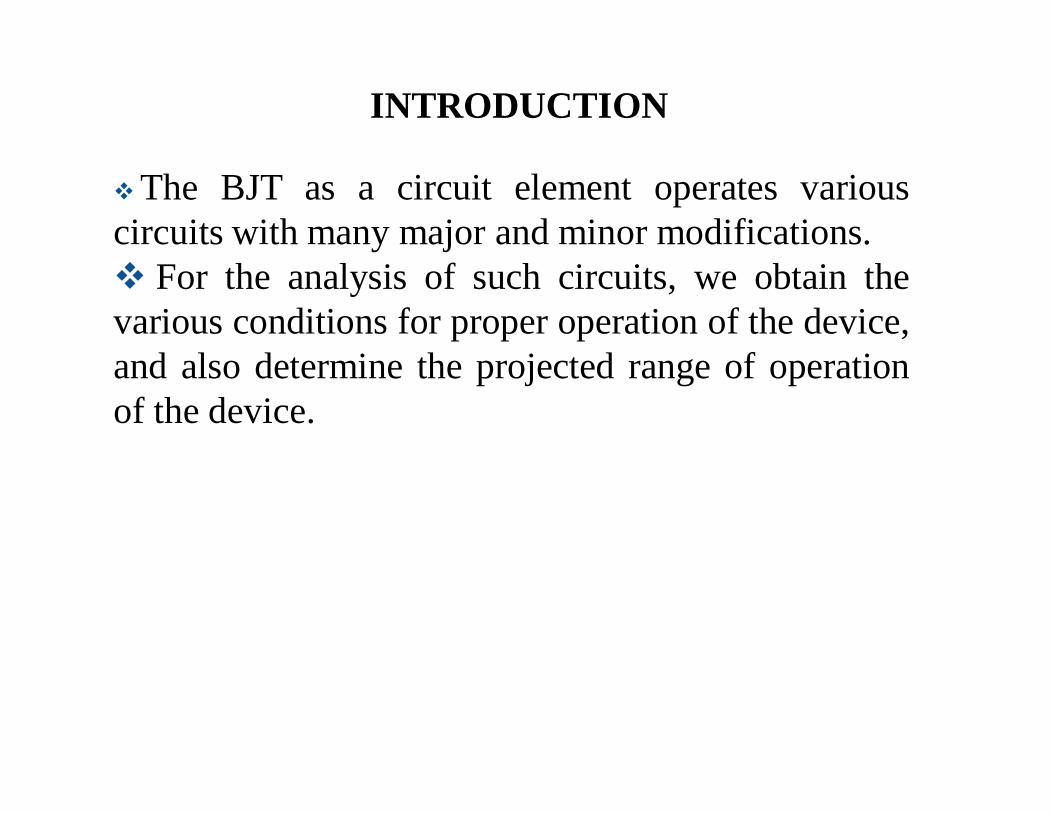
INTRODUCTION
The BJT as a circuit element operates variouscircuits with many major and minor modifications. For the analysis of such circuits, we obtain thevarious conditions for proper operation of the device,and also determine the projected range of operationof the device.

A detailed study of the device in a two-port modesimplifies the circuit analysis of the device to a largeextent. Thus, we calculate the various parameters of thedevices’ performance, namely voltage gain, currentgain, input impedance, and output impedance. The frequency response of the device is dealt within detail, and a study of the various regions ofoperation in the frequency scale is also explained. Finally, we will discuss the various configurationsof the device and take a look into the high-frequencyoperation of the device and its performance in thoseregions.

Proper Transistor Biasing
• For a transistor to function properly as an amplifier, the emitter-base junction must be forward-biased and the collector-base junction must be reverse-biased.
• The common connection for the voltage sources are at the base lead of the transistor.
• The emitter-base supply voltage is designated VEEand the collector-base supply voltage is designated VCC.
• For silicon, the barrier potential for both EB and CB junctions equals 0.7 V

6
Transistor Biasing
The basic function of transistor is amplification.The process of raising the strength of weak signalwithout any change in its general shape is referredas faithful amplification. For faithful amplificationit is essential that:-
1. Emitter-Base junction is forward biased2. Collector- Base junction is reversed biased3. Proper zero signal collector current
The proper flow of zero signal collector current andthe maintenance of proper collector emitter voltageduring the passage of signal is called transistorbiasing.

7
Why Biasing? If the transistor is not biased properly, it would
work inefficiently and produce distortion in output signal.
How A Transistor Can Be Biased?A transistor is biased either with the help of batteryor associating a circuit with the transistor. The latermethod is more efficient and is frequently used. Thecircuit used for transistor biasing is called the biasingcircuit.

8
BIAS STABILITY
Through proper biasing, a desired quiescent operatingpoint of the transistor amplifier in the active region(linear region) of the characteristics is obtained. It isdesired that once selected the operating point shouldremain stable. The maintenance of operating point stableis called Stabilisation.

The selection of a proper quiescent point generallydepends on the following factors:
(a)The amplitude of the signal to be handled bythe amplifier and distortion level in signal
(b)The load to which the amplifier is to work for acorresponding supply voltage
The operating point of a transistor amplifier shiftsmainly with changes in temperature, since thetransistor parameters — β, ICO and VBE (where thesymbols carry their usual meaning)—are functions oftemperature.

10
The DC Operating Point
For a transistor circuit to amplify it must be properlybiased with dc voltages. The dc operating pointbetween saturation and cutoff is called the Q-point.The goal is to set the Q-point such that that it does notgo into saturation or cutoff when an a ac signal isapplied.

11
The Thermal Stability of Operating Point (SIco)
Stability Factor S:- The stability factor S, asthe change of collector current with respect to thereverse saturation current, keeping β and VBEconstant. This can be written as:
The Thermal Stability Factor : The Thermal Stability Factor : SSIcoIco
SSIcoIco = = ∂∂IIcc
∂∂IIcoco VVbebe,, ββ

This equation signifies that Ic Changes SIco times as fast as Ico
Differentiating the equation of Collector Current IC =(1+β)Ico+ βIb & rearranging the terms we can write
SIco ═ 1+β ⧵و 1- β (∂Ib/∂IC)
It may be noted that Lower is the value of SIco better is the stability

13
Various Biasing Circuits
• Fixed Bias Circuit
• Fixed Bias with Emitter Resistor
• Collector to Base Bias Circuit
• Potential Divider Bias Circuit

14
The Fixed Bias Circuit
15 V
C
E
B
15 V
200 k 1 k
The Thermal Stability Factor : SIco
SIco = ∂Ic
∂Ico
General Equation of SIco Comes out to
SIco ═ 1 + β11-- ββ ((∂∂IIbb//∂∂IICC))
VVbebe, , ββ
IIbb
RRbbRRCC
RRCC

Applying KVL through Base Circuit we can write,
Ib Rb+ Vbe= Vcc
Diff w. r. t. IC, we get
(∂Ib / ∂Ic) = 0
SIco= (1+β) is very large Indicating high un-stability

16
Merits:• It is simple to shift the operating point anywhere in
the active region by merely changing the baseresistor (RB).
• A very small number of components are required.
Demerits:• The collector current does not remain constant with
variation in temperature or power supply voltage.Therefore the operating point is unstable.

• When the transistor is replaced with another one,considerable change in the value of β can be expected.Due to this change the operating point will shift.
• For small-signal transistors (e.g., not power transistors)with relatively high values of β (i.e., between 100 and200), this configuration will be prone to thermalrunaway. In particular, the stability factor, which is ameasure of the change in collector current with changesin reverse saturation current, is approximately β+1. Toensure absolute stability of the amplifier, a stabilityfactor of less than 25 is preferred, and so small-signaltransistors have large stability factors.

18
The fixed bias circuit ismodified by attaching anexternal resistor to theemitter. This resistorintroduces negativefeedback that stabilizes theQ-point.
Fixed bias with emitter resistor

19
Merits:
• The circuit has the tendency to stabilize operatingpoint against changes in temperature and β-value.
Demerits:
• As β-value is fixed for a given transistor, this relationcan be satisfied either by keeping RE very large, ormaking RB very low.

20
The Collector to Base Bias Circuit
VCC
RC
C
E
B
RF
IIccIIbb
VVBEBE++
-- IIEE
This configuration employsnegative feedback to preventthermal runaway and stabilizethe operating point. In this formof biasing, the base resistor RFis connected to the collectorinstead of connecting it to theDC source Vcc. So any thermalrunaway will induce a voltagedrop across the Rc resistor thatwill throttle the transistor's basecurrent.

21
Applying KVL through base circuit
we can write (Ib+ IC) RC + Ib Rf+ Vbe= Vcc
Diff. w. r. t. IC we get (∂Ib / ∂Ic) = - RC / (Rf + RC)
Therefore, SIco ═ (1+ β) 1+ [βRC/(RC+ Rf)]
Which is less than (1+β), signifying better thermal stability

22
Merits: • Circuit stabilizes the operating point againstvariations in temperature
and β (i.e. replacement of transistor)Demerits:• As β -value is fixed (and generally unknown) for a given transistor, this relation can be satisfied either by keeping Rc fairly large or making Rf very low.
Usage: The feedback also decreases the inputimpedance of the amplifier as seen from the base,which can be advantageous. Due to the gainreduction from feedback, this biasing form is usedonly when the trade-off for stability is warranted.

23
This is the most commonly used arrangement forbiasing as it provide good bias stability. In thisarrangement the emitter resistance ‘RE’RE’ providesstabilization. The resistance ‘RE’RE’ cause a voltage dropin a direction so as to reverse bias the emitterjunction. Since the emitter-base junction is to beforward biased, the base voltage is obtained from R1-R2 network.
The Potential Divider Bias Circuit

The Potential Divider Bias Circuit
• The net forward bias across the emitter base junction is equal to VB- dc voltage drop across ‘RE’RE’. The base voltage is set by Vcc and R1 and R2. The dc bias circuit is independent of transistor current gain. In case of amplifier, to avoid the loss of ac signal, a capacitor of large capacitance is connected across RE. The capacitor offers a very small reactance to ac signal and so it passes through the condensor.

25
VCC
RC
C
E
B
VCC
R1
RE R2 IIEE
IICC
IIbb
The Potential Divider Bias Circuit
To find the stability of this circuitwe have to convert this circuitinto its Thevenin’s Equivalentcircuit
RRthth == RR11*R*R2 2 && VVthth == Vcc RVcc R22RR11+R+R2 2 RR11+R+R22
VCC
RC
C
E
B
VCC
R1
RE R2
RRthth == RR11*R*R2 2 && VVthth == Vcc RVcc R22RR11+R+R2 2 RR11+R+R22
Rth = R1*R2 & Vth = Vcc R2R1+R2 R1+R2

Applying KVL through input base circuit
we can write IbRTh + IE RE+ Vbe= VTh
Therefore, IbRTh + (IC+ Ib) RE+ VBE= VTh
Diff. w. r. t. IC & rearranging we get (∂Ib / ∂Ic) = - RE / (RTh + RE)
Therefore,
Thevenin Thevenin Equivalent CktEquivalent Ckt
ThRRR
E
EIcoS
1
1
The Potential Divider Bias Circuit
VCC
RC
C
E
B
RE
RTh
VTh _ +
Thevenin Thevenin Equivalent VoltageEquivalent Voltage
SelfSelf--bias Resistorbias Resistor
IIEE
IIbbIICC

27
Merits:
• Operating point is almost independent of β variation. • Operating point stabilized against shift in temperature.
Demerits:
• As β-value is fixed for a given transistor, this relationcan be satisfied either by keeping RE fairly large, ormaking R1||R2 very low.

If RE is of large value, high VCC is necessary. This increases cost as well
as precautions necessary while handling.
AC as well as DC feedback is caused by RE, which reduces the AC voltage gain of the amplifier. A method to avoid AC feedback while retaining DC feedback is discussed below.

Usage:The circuit's stability and merits as above make it widelyused for linear circuits. If R1 || R2 is low, either R1 is low, orR2 is low, or both are low. A low R1 raises VB closer to VC,reducing the available swing in collector voltage, andlimiting how large RC can be made without driving thetransistor out of active mode. A low R2 lowers Vbe, reducingthe allowed collector current. Lowering both resistor valuesdraws more current from the power supply and lowers theinput resistance of the amplifier as seen from the base.

Biasing And Bias Stability
Biasing refers to the establishment of suitable dcvalues of different currents and voltages of a transistor. Through proper biasing, a desired quiescent operatingpoint of the transistor amplifier in the active region(linear region) of the characteristics is obtained. The selection of a proper quiescent point generallydepends on the following factors:
(a)The amplitude of the signal to be handled by theamplifier and distortion level in signal
(b)The load to which the amplifier is to work for acorresponding supply voltage

The operating point of a transistor amplifier shiftsmainly with changes in temperature, since thetransistor parameters — β, ICO and VBE (where thesymbols carry their usual meaning)—are functions oftemperature.
Circuit Configurations Fixed-bias circuit Fixed bias with emitter resistance Voltage-divider bias Voltage-feedback biasing

Biasing And Bias Stability
(a) Representation of fixed-bias circuit (b) Equivalent circuit
Fixed-bias circuit Base–emitter loop Collector–emitter loop
and

Biasing And Bias Stability
Fixed bias with emitter resistance Base–emitter loop
and the emitter current can be written as
From above two equation we get:
Collector–emitter loop

Fixed-bias circuit with emitter resistance
with the base current known, IC can be easilycalculated by the relation IC = βIB.

Biasing And Bias Stability
Voltage-divider bias:- The Thevenins equivalent voltage and resistance for the input side is given by:
Voltage-divider bias circuit Simplified voltage-divider circuit
The KVL equation for the input circuit is given as:

Biasing And Bias Stability
Representation of Voltage-feedback biased circuit
Voltage-feedback biasing Base–emitter loopApplying KVL for this part, we get:
Thus, the base current can be obtained as:

Biasing And Bias Stability
Stabilization Against Variations in ICO, VBE , and βTransfer characteristic:- In this particularcharacteristic, the output current IC is a function ofinput voltage for the germanium transistor. Thus,the word “transfer” is used for this characteristic.
Transfer characteristics for germanium p–n–p alloy type transistor

Collector current vs. base-to-emitter voltage for a silicon transistor
Self-bias circuit
Biasing And Bias Stability

Variation of the collector current with temperature because of VBE, ICO and β
Biasing And Bias Stability

Transistor Biasing
• For a transistor to function properly as an amplifier,an external dc supply voltage must be applied toproduce the desired collector current.
• Bias is defined as a control voltage or current.• Transistors must be biased correctly to produce the
desired circuit voltages and currents.• The most common techniques used in biasing are
– Base bias– Voltage-divider bias– Emitter bias

Transistor Biasing
Fig. -1
Fig. -1 (a) shows the simplest way to bias a transistor, called base bias. VBB is the base supply voltage, which is used to forward-bias the base-emitter junction. RB is used to provide the desired value of base current. VCC is the collector supply voltage, which provides the reverse-bias voltage required for the collector-base junction. The collector resistor, RC, provides the desired voltage in the collector circuit

Transistor Biasing: Base Biasing
• A more practical way to provide base bias is to use one power supply.
IB = VCC - VBE
RB
IC dc x IB
VCE VCC - ICRC

Transistor Biasing
Fig. 1
The DC load line is a graph that allows us to determine all possible combinations of IC and VCE for a given amplifier.
For every value of collector current, IC, the corresponding value of VCE can be found by examining the dc load line.
A sample dc load line is shown in Fig. 1.

Transistor BiasingMidpoint Bias
• Without an ac signal applied to a transistor, specific values of IC and VCE exist at a specific point on a dc load line
• This specific point is called the Q point (quiescent currents and voltages with no ac input signal)
• An amplifier is biased such that the Q point is near the center of dc load line– ICQ = ½ IC(sat)
– VCEQ = ½ VCC
• Base bias provides a very unstable Q point, because IC and VCE are greatly affected by any change in the transistor’s beta value

Transistor Biasing
Fig. 2
Fig. 2 illustrates a dc load line showing the end points IC (sat) and VCE (off), as well as the Q point values ICQand VCEQ.

Transistor Biasing
Fig. 28-18
The most popular way to bias a transistor is with voltage-divider bias. The advantage of voltage-divider bias lies in its stability.An example of voltage-divider bias is shown in Fig. 28-18.
VB = X VCCR2
R1 + R2
VE = VB - VBE
IE IC

Voltage Divider Bias – Example
• Solve for VB, VE, IE, IC, VC and VCE
• Construct a dc load line showing the values of IC(sat), VCE(off), ICQ and VCEQ
Transistor Biasing
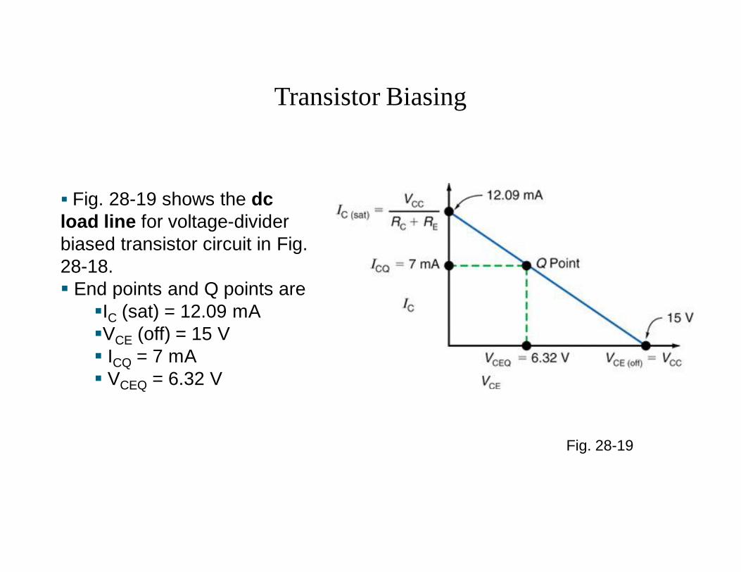
Fig. 28-19
Fig. 28-19 shows the dc load line for voltage-divider biased transistor circuit in Fig. 28-18. End points and Q points are
IC (sat) = 12.09 mAVCE (off) = 15 V ICQ = 7 mA VCEQ = 6.32 V

Calculation Of Stability Factors
Stability Factor S:- The stability factor S, as thechange of collector current with respect to the reversesaturation current, keeping β and VBE constant. This canbe written as:
Stability Factor S’:- The variation of IC with VBE isgiven by the stability factor S defined by the partialderivative:
Or,

Stability Factor S″:- The variation of IC withrespect to β is represented by the stability factor,S'', given as:
General Remarks on Collector CurrentStability:- The stability factors have been definedearlier keeping in mind the change in collectorcurrent with respect to changes in ICO , VBE and β.These stability factors are repeated here forsimplicity.

Thermal RunawayThe maximum average power in which a transistor can dissipate depends upon the construction of transistor and lie in the range of few milliwatts and 200W. The maximum power is limited by the temperature that the collector Base junction can withstand. The maximum power dissipation is usually specified for the transistor enclosure is 25 degree celsius. The junction temperature may increase either because of rise in ambient temperature or because of self heating. The problem of self heating arises due to dissipation of power at the collector junction.

The leakage current Icbo is extremely temperature dependent and increases with the rise in temperature of collector-base junction. With the increase in collector current Ic, collector power dissipation increases which raises the junction temperature that leads to further increase in collector current Ic. The process is cumulative and may lead to the eventual destruction of transistor. This phenomenon is known as THERMAL RUNAWAY of transistor. In practice the Thermal Runaway can be prevented by a well designed circuit called as STABILIZATION Circuitry.

Diode Compensation Techniques
Compensation for VBE:
Diagram shows the voltage divider bias with bias compensation technique.Here, separate supply VDD is used to keep diode in forward If biased condition. If the diode used in the circuit is of same material and type as the transistor, the voltage across the diode will have the same temperature coefficient as the base to emitter voltage VBE . So when VBE changes by ∂ VBE with change in temperature, VD changes by VD and ∂ VD~=~∂ VBE, the changes tend to cancel each other. Apply*g KVL to the base circuit of Fig. ,we have


Diode is connected in series with resistance R2 in thevoltage divider circuit and it is forward biased condition.For voltage divider bias,
When VBE changes with temperature, IC also changes
To cancel the changes in IC , one diode is used in thecircuit for compensation

Compensation for ICO
* In germanium transistor changes in ICO with temperature plays an important role collector current stability
* The diode is kept at reverse bias condition ,so only leakage current flows
* Io increases then ICO also increases


Thermistor Compensation

Fig (b) shows another thermistor compensation technique. Here, thermistor is connected between emitter and Vccto minimize the increase in collector current due tochanges in ICO, VBE, or beta with temperature.IC increases with temperature and RT decreases withincrease in temperature. Therefore, current flowingthrough RE increases, which increases the voltage dropacross it. E - B junction is forward biased. But due toincrease in voltage drop across RE, emitter is made morepositive, which reduces the forward bias voltage VBE.Hence, bias current reduces.
As Ico increases with temperature, IB decreases andhence. IC remains constant

Sensistor Compensation technique

This method of transistor compensation usestemperature sensitive resistive element, sensistorsrather than diodes or transistors. It has a positivetemperature coefficient, its resistance increasesexponentially with increasing temperature as shown inthe Fig
Slope of this curve =
is the temperature coefficient for thermistor andthe slope is positive So we can say that sensistor haspositive temperature coefficient of resistance (PTC).

Biasing Circuits used for JFET
• Fixed bias circuit• Self bias circuit• Potential Divider bias circuit

JFET (n-channel) Biasing Circuits
2
1
P
GSDSSDS V
VII
0, GGSGSGGGG IFixedVVRIV
DDSDDDS
P
GSDSSDS
RIVVV
VII
and
12
S
GSDS
SDSGS
RVI
RIV
0
For Self Bias Circuit
For Fixed Bias CircuitApplying KVL to gate circuit we get
and
Where, Vp=VGS-off & IDSS is Short ckt. IDS

JFET JFET BiasingBiasing Circuits Circuits ContdContd……or Fixed Bias Ckt.

JFET Self (or Source) Bias Circuit
2
1 and
P
GSDSSDS V
VII
S
GS
P
GSDSS R
V
V
VI
2
1
021
2
S
GS
P
GS
P
GSDSS R
V
V
V
V
VI
This quadratic equation can be solved for VGS & IDS

The Potential (Voltage) Divider Bias
01
2
S
GSG
P
GSDSS R
VV
V
VI
DSGSI V gives equation quadratic this Solving and

DC analysis step for Feedback Biasing Enhancement DC analysis step for Feedback Biasing Enhancement type MOSFETtype MOSFET
Find k using the datasheet or specification given;Find k using the datasheet or specification given;ex: Vex: VGS(ON)GS(ON),V,VGS(TH)GS(TH)
Plot transfer characteristics using the formula Plot transfer characteristics using the formula IIDD=k(V=k(VGSGS –– VVTT))22. Three point already defined that is . Three point already defined that is IID(ON)D(ON), V, VGS(ON)GS(ON) and Vand VGS(TH)GS(TH)
Plot a point that is slightly greater than VPlot a point that is slightly greater than VGSGS
Plot the linear characteristics (network bias line)Plot the linear characteristics (network bias line) The intersection defines the QThe intersection defines the Q--pointpoint
68

Again plot the line and the transfer curve to find the Q-point.Using the following equations:
21
DD2G
RRVRV
)( DSDDDDS
SDGGS
RRIVVRIVV
Input loop :
Output loop :
Voltage-Divider Biasing
69

UNIT II LARGE SIGNAL AMPLIFIERS
• Class A, AB, B, C and D type of operation, efficiency of Class A amplifier with resistive and transformer coupled load, efficiency of Class B, ComplementrySymmetry amplifiers, MOSFET Power amplifiers, Thermal stability of Power amplifiers, heat sink design

Classes of AmplifiersIntroduction
One method used to distinguish the electrical characteristics of different types of amplifiers is by “class”, and as such amplifiers are classified according to their circuit configuration and method of operation. Then Amplifier Classes is the term used to differentiate between the different amplifier types.

Amplifier Classes represent the amount of the output signal which varies within the amplifier circuit over one cycle of operation when excited by a sinusoidal input signal. The classification of amplifiers range from entirely linear operation (for use in high-fidelity signal amplification) with very low efficiency, to entirely non-linear (where a faithful signal reproduction is not so important) operation but with a much higher efficiency, while others are a compromise between the two.

Amplifier classes are mainly lumped into two basic groups. The first are the classically controlled conduction angle amplifiers forming the more common amplifier classes of A, B, AB and C, which are defined by the length of their conduction state over some portion of the output waveform, such that the output stage transistor operation lies somewhere between being “fully-ON” and “fully-OFF”.

The second set of amplifiers are the newer so-called “switching” amplifier classes of D, E, F, G, S, T etc, which use digital circuits and pulse width modulation (PWM) to constantly switch the signal between “fully-ON” and “fully-OFF” driving the output hard into the transistors saturation and cut-off regions.

Class A Amplifier

To achieve high linearity and gain, the output stage of a class A amplifier is biased “ON” (conducting) all the time. Then for an amplifier to be classified as “Class A” the zero signal idle current in the output stage must be equal to or greater than the maximum load current (usually a loudspeaker) required to produce the largest output signal.As a class A amplifier operates in the linear portion of its characteristic curves, the single output device conducts through a full 360 degrees of the output waveform. Then the class A amplifier is equivalent to a current source.

Class B Amplifier
Class B amplifiers were invented as a solution to the efficiency and heating problems associated with the previous class A amplifier. The basic class B amplifier uses two complimentary transistors either bipolar of FET for each half of the waveform with its output stage configured in a “push-pull” type arrangement, so that each transistor device amplifies only half of the output waveform.
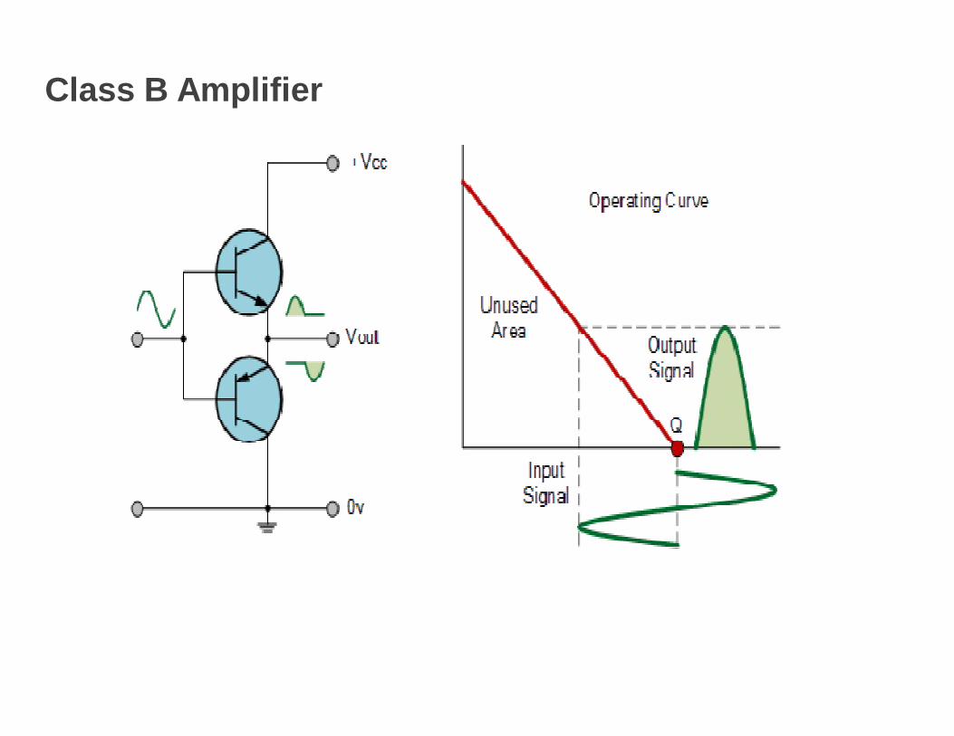
Class B Amplifier

When the input signal goes positive, the positive biased transistor conducts while the negative transistor is switched “OFF”. Likewise, when the input signal goes negative, the positive transistor switches “OFF” while the negative biased transistor turns “ON” and conducts the negative portion of the signal. Thus the transistor conducts only half of the time, either on positive or negative half cycle of the input signal.Then we can see that each transistor device of the class B amplifier only conducts through one half or 180 degrees of the output waveform in strict time alternation, but as the output stage has devices for both halves of the signal waveform the two halves are combined together to produce the full linear output waveform.

Class AB AmplifierAs its name suggests, the Class AB Amplifier is a combination of the “Class A” and the “Class B” type amplifiers we have looked at above. The AB classification of amplifier is currently one of the most common used types of audio power amplifier design. The class AB amplifier is a variation of a class B amplifier as described above, except that both devices are allowed to conduct at the same time around the waveforms crossover point eliminating the crossover distortion problems of the previous class B amplifier.

Class AB Amplifier

The advantage of this small bias voltage, provided by series diodes or resistors, is that the crossover distortion created by the class B amplifier characteristics is overcome, without the inefficiencies of the class A amplifier design. So the class AB amplifier is a good compromise between class A and class B in terms of efficiency and linearity, with conversion efficiencies reaching about 50% to 60%.

Class C AmplifierThe Class C Amplifier design has the greatest efficiency but the poorest linearity of the classes of amplifiers mentioned here. The previous classes, A, B and AB are considered linear amplifiers, as the output signals amplitude and phase are linearly related to the input signals amplitude and phase.However, the class C amplifier is heavily biased so that the output current is zero for more than one half of an input sinusoidal signal cycle with the transistor idling at its cut-off point.

Class C Amplifier

Due to its heavy audio distortion, class C amplifiers are commonly used in high frequency sine wave oscillators and certain types of radio frequency amplifiers, where the pulses of current produced at the amplifiers output can be converted to complete sine waves of a particular frequency by the use of LC resonant circuits in its collector circuit.

Class D Power Amplifier

A Class D audio amplifier is basically a non-linear switching amplifier or PWM amplifier. Class-D amplifiers theoretically can reach 100% efficiency, as there is no period during a cycle were the voltage and current waveforms overlap as current is drawn only through the transistor that is on.

Amplifier Classes and Efficiency

Amplifier Class Description Conduction
Angle
Class-A Full cycle 360o of Conduction θ = 2π
Class-B Half cycle 180o of Conduction θ = π
Class-AB Slightly more than 180o of conduction π < θ < 2π
Class-C Slightly less than 180o of conduction θ < π
Class-D to T
ON-OFF non-linear switching θ = 0
Amplifier Class by Conduction Angle

Crossover Distortion When the dc base voltage is zero, both transistors are
off and the input signal voltage must exceed VBE before a transistor conducts.
Because of this, there is a time interval between the positive and negative alternations of the input when neither transistor is conducting, as shown in Figure.
The resulting distortion in the output waveform is called crossover distortion.


Thermal stability of Power amplifiers
• Each heat-sink has a parameter called its Thermal Resistance (Rth) measured in °C/Watt and the lower the value of Rth the faster heat is dissipated. Other factors affecting heat dissipation include the power (in Watts) being dissipated by the transistor, the efficiency of heat transfer between the internal transistor junction and the transistor case, and the case to the heat-sink. The difference between the temperature of the heatsink and the air temperature surrounding the heat-sink (the ambient temperature) must also be taken into account. The main criterion is that the heat-sink should be efficient enough, too efficient is not a problem.

Heat Sinks
A heat-sink is designed to remove heat from atransistor and dissipate it into the surrounding airas efficiently as possible. Heat-sinks take manydifferent forms, such as finned aluminium orcopper sheets or blocks, often painted or anodisedmatt black to help dissipate heat more quickly. Aselection of heat-sinks is illustrated in Fig. 5.1.3.

Heat Sinks

Good physical contact between the transistor and heat-sink is essential, and a heat transmitting grease (heat-sink compound) is smeared on the contact area before clamping the transistor to the heat-sink. Where it is necessary to maintain electrical insulation between transistor and heat-sink a mica layer is used between the heat-sink and transistor. Mica has excellent insulation and very good heat conducting properties.

UNIT III FEEDBACK AMPLIFIERS
Types of feedback, Effect of feedback on noise,distortion, gain, input and output impedanceof the amplifiers, Analysis of Voltage andCurrent feedback amplifiers, NegativeResistance Oscillator, Barhausen Criterion foroscillation in feedback oscillator,

Mechanism for start of oscillation andstabilization of amplitude, Analysis of RCOscillators using Cascade connection of Lowpassand Highpass filters, Wein Phase shift and twin-Tnetwork, Analysis of LC Oscillators, Colpitts,Hartley, Clapp, Franklin, Armstrong and MillerOscillator, Quartz Crystal Oscillator circuits.
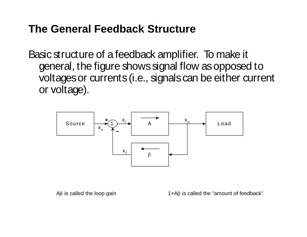
Basic structure of a feedback amplifier. To make it general, the figure shows signal flow as opposed to voltages or currents (i.e., signals can be either current or voltage).
A is called the loop gain 1+A is called the “amount of feedback”
S ource A
Loadxs
x f
x i xo
The General Feedback Structure

AA
xxA
s
of
1
The open-loop amplifier has gain A xo = A*xi
Output is fed back through a feedback network which produces a sample (xf) of the output (xo) xf = bxo
Where b is called the feedback factor The input to the amplifier is xi = xs – xf (the
subtraction makes feedback negative) Implicit to the above analysis is that neither the
feedback block nor the load affect the amplifier’s gain (A). This not generally true and so we will later
see how to deal with it.

Negative Feedback Properties
Negative feedback takes a sample of the output signal and applies it to the input to get several desirable properties. In amplifiers, negative feedback can be applied to get the following properties
–Desensitized gain – gain less sensitive to circuit component variations

Reduce nonlinear distortion – output proportional to input (constant gain independent of signal level)
–Reduce effect of noise
–Control input and output impedances – by applying appropriate feedback topologies
–Extend bandwidth of amplifier
These properties can be achieved by trading off gain

Gain Desensitivity
Feedback can be used to desensitize the closed-loop gain to variations in the basic amplifier. Let’s see how.
Assume beta is constant. Taking differentials of the closed-loop gain equation gives…
Divide by Af
21 AdAdAf
AdA
AAA
AdA
AdA
f
f
1
111 2
AAAf
1
This result shows the effects of variations in A on Afis mitigated by the feedback amount. 1+Abeta is also called the desensitivity amount
We will see through examples that feedback also affects the input and resistance of the amplifier (increases Ri and decreases Ro by 1+Abeta factor)

Bandwidth Extension
We’ve mentioned several times in the past that we can trade gain for bandwidth. Finally, we see how to do so with feedback… Consider an amplifier with a high-frequency response characterized by a single pole and the expression: Apply negative feedback beta and the resulting closed-loop gain is:

H
M
sAsA
1
MH
MMf As
AAsA
sAsA
111
1
•Notice that the midband gain reduces by (1+AMbeta) while the 3-dB roll-off frequency increases by (1+AMbeta)

Basic Feedback Topologies
Depending on the input signal (voltageor current) to be amplified and formof the output (voltage or current),amplifiers can be classified into fourcategories. Depending on theamplifier category, one of four typesof feedback structures should be used(series-shunt, series-series, shunt-shunt, or shunt-series) Voltageamplifier – voltage-controlled voltagesource Requires high inputimpedance, low output impedance
series-shunt
shunt-series
series-series
shunt-shunt

Use series-shunt feedback (voltage-voltage feedback) Current amplifier – current-controlled current source Use shunt-series feedback (current-current feedback) Transconductance amplifier – voltage-controlled current source Use series-series feedback (current-voltage feedback) Transimpedance amplifier – current-controlled voltage source Use shunt-shunt feedback (voltage-current feedback)

Series-Shunt Feedback Amplifier(Voltage-Voltage Feedback)
Samples the output voltageandreturns a feedback voltagesignalIdeal feedback network hasinfinite input impedance andzero output resistanceFind the closed-loop gain andinput resistance
ARR o
of
1

The output resistance can be found byapplying a test voltage to the outputSo, increases input resistance andreduces output resistance makesamplifier closer to ideal VCVS

The Series-Shunt Feedback Amplifier
The Ideal Situation
The series-shunt feedback amplifier:
(a)ideal structure; (b)equivalent circuit.
AfVo
Vs
A1 A
RifVs
Ii
Vs
Vi
Ri
RiVs
Vi Ri
Vi A Vi
Vi
Rif Ri 1 A
Zif s( ) Zi s( ) 1 A s( ) s( )
Z of s( )Z o s( )
1 A s( ) s( )
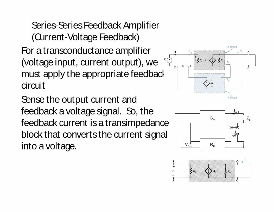
Series-Series Feedback Amplifier(Current-Voltage Feedback)
For a transconductance amplifier (voltage input, current output), we must apply the appropriate feedback circuit Sense the output current and feedback a voltage signal. So, the feedback current is a transimpedanceblock that converts the current signal into a voltage.
Gm
RF
Iout
ZL
Itst
Vf

)mG called (also i
o
VIA
AA
VIA
s
of
1
fmtst
out RGIIA Gain Loop
ARI
VAIRI
IIRI
VVIVR i
i
iii
i
oii
i
fi
i
sif
1
otst
otsttst
tst
oitst
tst
tstof RA
IRIAI
IRAVI
IVR
1

Shunt-Shunt Feedback Amplifier(Voltage-Current Feedback
• When voltage-current FB is applied to a transimpedanceamplifier, output voltage is sensed and current is subtracted from the input
ARR iif 1 ARR o
of
1

AA
IVA
VA
VIII
IVA
s
of
oo
fis
i
o
1
– The gain stage has some resistance – The feedback stage is a transconductor – Input and output resistances (Rif and Rof)
follow the same form as before based on values for A and beta
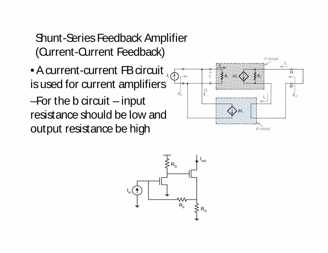
Shunt-Series Feedback Amplifier(Current-Current Feedback)
•A current-current FB circuit is used for current amplifiers –For the b circuit – input resistance should be low and output resistance be high
Iout
Iin
RSRF
RD

•A circuit example is shown –RS and RF constitute the FB circuit •RS should be small and RF large –The same steps can be taken to solve for A, Abeta, Af, Rif, and Rof
•Remember that both A and b circuits are current controlled current sources

Negative Resistance Oscillator
Negative resistance is a property ofsome electric circuits where an increase in thecurrent entering a port results in a decreasedvoltage across the same port.

•The circuit helps generate microwave frequencies upto 100 GHz.•The tunnel diode is connected in series with the tank circuit. •When power is applied surge current produces oscillation in the tank. R and C values will make DC bias at the center of negative resistance curve of tunnel diode. •Sustained oscillation results when magnitude of negative resistance of tunnel diode is greater or equal to positive resistance of the tank circuit.

Oscillators
• Oscillator is an electronic circuit that generates a periodic waveform on its output without an external signal source. It is used to convert dc to ac.
• Oscillators are circuits that produce a continuous signal of some type without the need of an input.
• These signals serve a variety of purposes. • Communications systems, digital systems
(including computers), and test equipment make use of oscillators

•An oscillator is a circuit that produces a repetitive signal from a dc voltage.
• The feedback oscillator relies on a positive feedback of the output to maintain the oscillations.
• The relaxation oscillator makes use of an RC timing circuit to generate a nonsinusoidal signal such as square wave.

Oscillators are used to generate signals, e.g.•Used as a local oscillator to transform the RF signals to IF signals in a receiver;•Used to generate RF carrier in a transmitter•Used to generate clocks in digital systems;•Used as sweep circuits in TV sets and CRO
Sine wave
Square wave
Sawtooth wave

Conditions for Barkhausen criterion
According to Barkhausen criterion for sustained oscillation:The magnitude of the product of open loop gain of the amplifier and the magnitude of the feedback factor is unity, i.e., |βA|=1|βA|=1 where A is the gain of the amplifying element in the circuit and β(jω)β(jω) is the transfer function of the feedback path.•The total phase shift around the loop is 00 or integral multiples of 2π2π.

Tank Circuit
•LC parallel circuit is called tank circuit.
• Once excited, it oscillates at

The energy keeps oscillating between electric potential energy and magnetic filed energy

Damped oscillations are produced.


RC OSCILLATORSThree types of feedback oscillators that use RC circuitsto produce sinusoidal outputs are theo Wien-bridge oscillatoro Phase-shift oscillatoro Twin-T oscillator-Generally, RC feedback oscillators are used forfrequencies up to about 1 MHz.-The Wien-bridge is by far the most widely used typeof RC feedback oscillator for this range of frequencies.

RC Phase Shift Oscillator

•The phase shift oscillator utilizes three RC circuits to provide 180º phase shift that when coupled with the 180º of the op-amp itself provides the necessary feedback to sustain oscillations.
•The gain must be at least 29 to maintain the oscillations.
•The frequency of resonance for the this type is similar to any RC circuit oscillator.

Wien bridge oscillator

Wien bridge oscillator
• The Wien bridge oscillator is essentially a feedback amplifier in which the Wien bridge serves as the phase-shift network.
• The Wien bridge is an ac bridge, the balance of which is achieved at one particular frequency.
• Frequency of Oscillation

LC Oscillators
• Colpitts Oscillator• Hartley Oscillator• Clapp Oscillator• Franklin Oscillator• Armstrong Oscillator• Miller Oscillator

Colpitts Oscillator

•One basic type of resonant circuit feedback oscillator is the Colpitts oscillator.•This type of oscillator uses an LC circuit in the feedback loop to provide the necessary phase shift and to act as a resonant filter that passes only the desired frequency of oscillation. •The approximate frequency of oscillation is the resonant frequency of the LC circuit and is established by the values of C1,C2,L and according to the formula:

Where CT is the total capacitance.•Because the capacitors effectively appear in series around the tank circuit, the total capacitance CT is

The Hartley Oscillator

The Hartley Oscillator
• The Hartley oscillator is similar to the Colpitts except that the feedback circuit consists of two series inductors and a parallel capacitor
• In this circuit, the frequency of oscillation for(Q>10) is
Where LT=L1+L2

The Clapp Oscillator

The Clapp Oscillator
• The Clapp oscillator is a variation of the Colpitts. • The basic difference is an additional capacitor
C3,in series with the inductor in the resonant feedback circuit
• Since C3 is in series with C1 and C2 around the tank circuit, the total capacitance is
and the approximate frequency of oscillation (Q>10) is

The Armstrong Oscillator

The Armstrong Oscillator
• This type of LC feedback oscillator uses transformer coupling to feed back a portion of the signal voltage.
• The transformer secondary coil provides the feedback to keep the oscillation going.
• The Armstrong is less common than the Colpitts, Clapp, and Hartley, mainly because of the disadvantage of transformer size and cost.
• The frequency of oscillation is set by the inductance of the primary winding(LPri) in parallel with C1.

Franklin Oscillator

Franklin Oscillator
• The Franklin Oscillator has 2 CE amplifier stages which gives phase shift from input to output.
• The frequency of oscillation is

Quartz Crystal
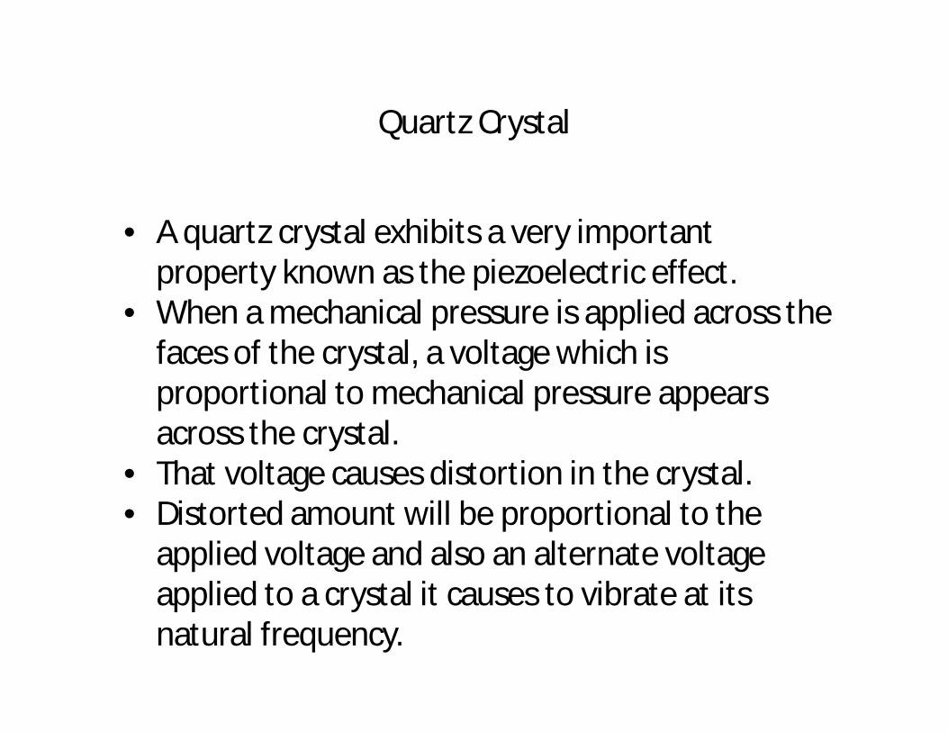
Quartz Crystal
• A quartz crystal exhibits a very important property known as the piezoelectric effect.
• When a mechanical pressure is applied across the faces of the crystal, a voltage which is proportional to mechanical pressure appears across the crystal.
• That voltage causes distortion in the crystal. • Distorted amount will be proportional to the
applied voltage and also an alternate voltage applied to a crystal it causes to vibrate at its natural frequency.

Quartz Crystal Oscillator

Quartz Crystal Oscillator
• The quartz crystal oscillator circuit diagram consists of two resonances such as series and parallel resonance, i.e., two resonant frequencies
• The series resonance occurs when the reactance produced by capacitance C1is equal and opposite to the reactance produced by inductance L.

UNIT IV TUNED AMPLIFIERS & MULTIVIBRATOR CIRCUITS
• Tank circuits.• Analysis of single tuned amplifier, Double tuned,
stagger tuned amplifiers. • Instability of tuned amplifiers, stabilization
techniques, Narrow band neutralization using coil, Broad banding using Hazeltine neutralization,
• Class C tuned amplifiers and their applications. Efficiency of Class C tuned Amplifier.
• Astable multivibrators, monostable and bistablemultivibrator using similar and complementary transistors, speed up capacitors,Schmitt trigger circuits.

Tuned Amplifier
• Definition
An amplifier circuit in which the load circuit is a tank circuit such that it can be tuned to pass or amplify selection of a desired frequency or a narrow band of frequencies, is known as Tuned Circuit Amplifier.

Tuned Amplifier Characteristics
• Tuned amplifier selects and amplifies a singlefrequency from a mixture of frequencies in anyfrequency range.
• A Tuned amplifier employs a tuned circuit.• It uses the phenomena of resonance, the tank circuit
which is capable of selecting a particular or relativenarrow band of frequencies.
• The centre of this frequency band is the resonantfrequency of the tuned circuit .
• Both types consist of an inductance L and capacitanceC with two element connected in series and parallel

Resonance Circuits
When at particular frequency the inductive reactance became equal to capacitive reactance and the circuit then behaves as purely resistive circuit. This phenomenon is called the resonance and the corresponding frequency is called the resonant frequency.
C L
Tuned circuit

Classification of Tuned Amplifier

Single Tuned Amplifiers

Single Tuned Amplifier

Single Tuned Amplifier
• Single Tuned Amplifier consist of only one Tank Circuit and the amplifing frequency range is Determined by it.
• By giving signal to its input terminal of various Frequency Ranges.
• The Tank Circuit on its collector delivers High Impedence on resonant Frequency.
• Thus the amplified signal is Completely Available on the output Terminal.
• And for input signals other than Resonant Frequency, the tank circuit provides lower imedence, hence most of the signals get attenuated at collector Terminal.

Limitations
• This tuned amplifier are required to be highlyselective. But high selectivity required a tuned circuitwith a high Q- factor .
• A high Q- factor circuit will give a high Av but atthe same time , it will give much reduced band withbecause bandwidth is inversely proportional to theQ- factor .
• It means that tuned amplifier with reducebandwidth may not be able to amplify equally thecomplete band of signals & result is poorreproduction . This is called potential instability intuned amplifier.

Double tuned amplifier

Double tuned amplifier
• Double tuned amplifiers consists of Inductively coupled two tuned circuits. One L1, C1 and the other L2, C2. In the Collector terminals.A change in the coupling of the two tuned circuits results in change in the shape of the Frequency response curve.
• By proper adjustment of the coupling between the two coils of the two tuned circuits, the required results(High selectivity, high Voltage gain and required bandwidth) may be obtained.

Volta
ge
gain
AV
Frequency fr
K=2
K=1.5K=1
fr
Critical coupling
Loose coupling
Resonance curve of Parallel Resonant circuit:

Stagger Tuned Amplifier

Stagger Tuned Amplifier
• Stagger Tuned Amplifiers are used to improve the overall frequency response of tuned Amplifiers. Stagger tuned Amplifiers are usually designed so that the overall response exhibits maximal flatness around the centre frequency.
• It needs a number of tuned circuit operating in union. The overall frequency response of a Stagger tuned amplifier is obtained by adding the individual response together. Since the resonant Frequencies of different tuned circuits are displaced or staggered, they are referred as Stagger Tuned Amplifier.

The main advantage of stagger tuned amplifier is increased bandwidth. Its Drawback is Reduced Selectivity and critical tuning of many tank circuits. They are used in RF amplifier stage in Radio Receivers.The stagger tuning in this circuit is achieved by resonating the tuned circuits L1 C1, L2 C2 to slightly different Frequencies

Stagger Tuned Amplifier
Freq. response of first stage
Freq. response of second stage
Over all response
f1 f0 f2
Frequency
Volta
ge

Neutralization using coil

Neutralization using coil
• L part of the tuned circuit at the base o next stage is oriented or minimum coupling to the other winding. It is wound on a separate from and is mounted at right angle to the coupled windings. If the windings are properly polarized, the voltage across L due to the circulating current in the base circuit will have the proper phase to cancel the signal coupled through the base to collector, Cbc capacitance.

Hazeltine Neutralization

Hazeltine Neutralization
• In this circuit a small value of variable capacitance CN is connected from the bottom of coil, point B, to the base.
• Therefore, the internal capacitance Cbc, shown dotted, feeds a signal from the top end of the coil, point A, to the transistor base and the CN feeds a signal output equal magnitude but opposite polarity from the bottom output coil, point B, to the base.
• The neutralizing capacitor, CN can be adjusted correctly to completely nullify the signal fed through the Cbc

Class C Tuned Amplifier
• Class C amplifiers are biased so that conduction occurs formuch less than 180 degrees .
• Class C amplifiers are more efficient than either class A orpush-pull class B and class AB, which means that moreoutput power can be obtained from class C operation.
• The output amplitude is a nonlinear function of the input,so class C amplifiers are not used for linear amplification.
• They are generally used in radio frequency (RF)applications, including circuits, such as oscillators, thathave a constant output amplitude modulators, where ahigh-frequency signal is controlled by a low-frequencysignal.
• Therefore, Class C amplifiers are also called TunedAmplifiers.

Class C Tuned Amplifier

• Because the collector voltage (output) is not a replica of the input, the resistively loaded class C amplifier alone is of no value in linear applications.
• It is therefore necessary to use a class C amplifier with a parallel resonant circuit (tank).
• The short pulse of collector current on each cycle of the input initiates and sustains the oscillation of the tank circuit so that an output sinusoidal voltage is produced.
• The tank circuit has high impedance only near the resonant frequency, so the gain is large only at this frequency
Class C Tuned Amplifier

Sharpness of the Resonance Curve
• The resonance curve is required to be as sharp as possible in order to provide a high selectivity.
• A sharp resonance curve means that the impedance falls off rapidly as the frequency is varied above and below the resonant frequency.

Effect of Coil Resistance (R) on sharpness of the resonant curve

Applications of Tuned Amplifiers
Tuned amplifiers serve the best for two purposes:a)Selection of desired frequency.b)Amplifying the signal to a desired level.

Advantages
• It provides high selectivity.• It has small collector voltage.• Power loss is also less.• Signal to noise ratio of O/P is good.• They are well suited for radio transmitters and
receivers
Disadvantages
• They are not suitable to amplify audio frequencies.• If the band of frequency is increase then design
becomes complex.• Since they use inductors and capacitors as tuning
elements, the circuit is bulky and costly.

Multivibrators
• A Multivibrator is an electronic circuit that generates square, rectangular, pulse waveforms, also called nonlinear oscillators or function generators.
• Multivibrator is basically a two amplifier circuits arranged with regenerative feedback.
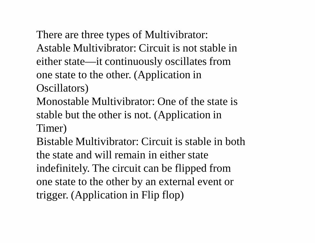
There are three types of Multivibrator:Astable Multivibrator: Circuit is not stable in either state—it continuously oscillates from one state to the other. (Application in Oscillators) Monostable Multivibrator: One of the state is stable but the other is not. (Application in Timer) Bistable Multivibrator: Circuit is stable in both the state and will remain in either state indefinitely. The circuit can be flipped from one state to the other by an external event or trigger. (Application in Flip flop)

Duty Cycle
• Duty cycle is defined as the ratio of pulse duration to pulse period.
The pulse duration is τ; this is how long the pulse remains high (amplitude=1 in the figure).The pulse period is T ; this is the duration of one complete cycle, and is just the inverse of the frequency in Hz (f = 1/T). D= τ / T

Astable Multivibrator
• The astable circuit has no stable state.• With no external signal applied, the transistors
alternately switch from cutoff to saturation at a frequency determined by the RC time constants of the coupling circuits.
• Astable multivibrator circuit consist of two cross coupled RC amplifiers.

Consists of two amplifying devices cross-coupled by resistors and capacitors. Typically, R2 = R3, R1 = R4, C1 = C2 and R2 >> R1. The circuit has two states State 1: VC1 LOW, VC2 HIGH, Q1 ON (saturation) and Q2 OFF. State 2: VC1 HIGH, VC2 LOW, Q1 OFF and Q2 ON (saturation).It continuously oscillates from one state to the other.

Astable Multivibrator

Monostable Multivibrators

Monostable Multivibrators
• One of the state is stable but the other is not. For that capacitive path between VC2 and VB1 removed.
• In stable state any one transistor conducts and other is off. Application of external trigger change the state.
• When the external signal goes high 8 VB2 charges up to VCC through R 2 .
• After a certain time T, VB2=VON, Q2 turns on VC2 pulled to 0V, Q1 turns off.
• Enters state 1 and remains there When VB2 is momentarily pulled to ground by an external signal
• VC2 rises to VCC Q1 turns on VC1 pulled to 0V

Bistable Multivibrators

Bistable Multivibrators
• Both capacitors removed • Stable for either state 1 or 2• Can be forced to either state by Set or Reset signals• If Set is low, • Q1 turns off • VC1 (Vout) and VB2 rises towards VCC • Q2 turns on

Bistable Multivibrators
• VC2 pulled to 0V • VB1 is latched to 0V• Circuit remains in state 2 until Reset is low • If Reset is low • Similar operation • Circuit remains in state 1 until Set is low • Behave as an RS flip-flop (memory element

Speed Up Capacitors
• Switching Characteristics can be improve by passing high frequency components of the pulses
• For this purpose small capacitances are used in shunt with the coupling resistorsR1.
• Due to this transition time reduces without affecting the stable states.
• These capacitors allows fast rise and fall times.• Hence they are called as Speed Up Capacitors.

Speed Up Capacitors
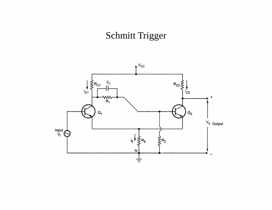
Schmitt Trigger

Schmitt Trigger
• Schmitt trigger circuit converts any type of wave in to a rectangular wave.
• When power is first switched on it gives a small forward bias to Q2 then it comes in to conducting state.

This current flows through R4 which gives a potential drop VE across R4 .This VE gives reverse bias to the base of Q1 .So it comes to off state then the voltage across Q1 will be equal to Vcc, and voltage across Q2 approaches to zero. So in this case. a) Q1 is in cut – off state and voltage across it is high.b) Q2 is in saturation or conducting state and voltage across it is low or zero..

Schmitt Trigger
• If the positive voltage of the sine wave from the signal generator is sufficient to over come the reverse bias of Q1, then Q1 comes in to conducting state and the negative going voltage is applied to the base of Q2 through R3 .
• This reduces the forward bias of Q2 and thus Q2 comes in to cut-off state.
• Then the voltage across it is high and voltage across Q1 is low.
•

The same process repeats with opposite sense when negative half cycle if in put of a.c. is applied. The combined effect generates a rectangular wave at the out put. Also the frequency of the rectangular wave is equal to the frequency of the a.c. input signal. The amplitude of the in put voltage required to put Q2 in to conducting state is called lower trigger potential (LTP). Similarly input voltage required to put Q1 in to conducting state is called upper trigger potential (UTP).

Schmitt Trigger

UNIT V RECTIFIERS, BLOCK OSCILLATORS AND TIMEBASE GENERATORS
• Half Wave Rectifier - Full Wave Rectifier – Bridge Rectifier – Performance of Rectifiers
• Filters – Types of Filters – L, C, LC, π Filters –Ripple Factor Calculation for C, L, LC and π Filter
• Regulators – Shunt and Series Voltage Regulator – IC Regulator SMPS – Power Control using SCR. RC and RL wave shaping circuits, UJT sawtoothgenerators, Linearization using constant current circuit, Bootstrap and Miller saw tooth generators, current time base generators, Time base circuits -Voltage-Time base circuit, Current-Time base circuit.

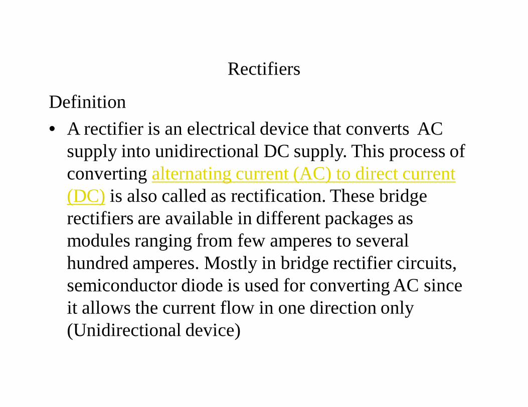
Rectifiers
Definition• A rectifier is an electrical device that converts AC
supply into unidirectional DC supply. This process of converting alternating current (AC) to direct current (DC) is also called as rectification. These bridge rectifiers are available in different packages as modules ranging from few amperes to several hundred amperes. Mostly in bridge rectifier circuits, semiconductor diode is used for converting AC since it allows the current flow in one direction only (Unidirectional device)


Half Wave RectifierIt is a simple type of rectifier made with single diode which is connected in series with load. For small power levels this type of rectifier circuit is commonly used.

During the positive half of the AC input, diode becomes forward biased and currents starts flowing through it. During the negative half of the AC input, diode becomes reverse biased and current stops flowing through it. Output waveform across the load is shown in figure. Because of high ripple content in the output, this type of rectifier is seldom used with pure resistive load.

The output DC voltage of a half wave rectifier can be
calculated with the following two ideal equations

Half wave rectifier

Half wave rectifier

AdvantageSimple circuit and low costDisadvantageThe output current in the load contains, in addition to dc component, ac components of basic frequency equal to that of the input voltage frequency. Ripple factor is high and an elaborate filtering is, therefore, required to give steady dc output.The power output and, therefore, rectification efficiency is quite low. This is due to the fact that power is delivered only half the time.Transformer Utilization Factor (TUF) is low.DC saturation of transformer core resulting in magnetizing current and hysteresis losses and generation of harmonics.

Full Wave Center-tapped RectifierThis type of rectifier uses two diodes and a transformer with center tapped secondary winding. During the positive half cycle of the input AC diode D1 is forward biased and the current starts flowing to the load through it. During the negative half of the input diode D2 forward biased and D1 becomes reverse biased. Load current start flowing through D2 during this negative peak. Note that the current flow through load has not changed even when the voltage polarity changed.


Full Wave Bridge RectifierUsing the same secondary voltage, this bridge rectifier can produce almost double the output voltage as compared with full wave center-tapped transformer rectifier. During the positive half of the input AC diodes D1 and D2 are forward biased and D3 and D4 are reverse biased. Thus load current flows through D1 and D2 diodes. During the negative half cycle of the input diodes D3&D4 are forward biased and D1&D2 are reverse biased. Therefore load current flows through D3&D4 diodes.


Advantages of bridge rectifierThe rectification efficiency of full-wave rectifier is double of that of a half-wave rectifier.Higher output voltage, higher output power and higher Transformer Utilization Factor in case of full-wave rectifier.The ripple voltage is low and of higher frequency in case of full-wave rectifier so simple filtering circuit is requiredNo center tap is required in the transformer secondary so in case of a bridge rectifier the transformer required is simpler.

If stepping up or stepping down of voltage is not required, transformer can be eliminated even.For a given power output, power transformer of smaller size can be used in case of the bridge rectifier because current in both primary and secondary windings of the supply transformer flow for the entire ac cycle2 Disadvantages of Bridge RectifierIt requires four diodes.The use of two extra diodes cause an additional voltage drop thereby reducing the output voltage.

Filters
• A filter circuit is a device to remove the AC components of the rectified output,but allow the DC component to reach the load.
• A filter circuit consists of passive circuit elements i.einductors,capacitors,resistors and their combination.

Types of Filters
• Inductor Filter• Capacitor Filter• LC Filter• ᴨ Filter

Inductor Filter

Inductor Filter
• Also called Choke Filter.• Consists of an inductor L which is inserted between
the Rectifier and the load resistance RL.• Rectifier contains AC as well as DC components• When output passes through inductor it offers a high
resistance to the AC component and no resistance to DC component.
• Therefore AC components of the rectified output is blocked and only DC components reached at the load.

Capacitor Filter

Capacitor Filter
• Capacitor is connected across the load.• During the rise of voltage it gets charge and is
supplied to the load during the fall in voltage cycle.• This process is repeated for each cycle and thus the
repel is reduced across the load.

LC Filter

LC Filter
• Choke is connected in series with load.• Offers high resistance to the AC components and
allows DC component to flow through the load.• The capacitor across the load is connected in parallel
which filter out any AC component flowing through the choke.

CLC or PIE Filter

CLC or PIE Filter
• Three components are arranged in shape of Greek letter Pi.
• Input capacitor is selected to offer very low reactance to the repel frequency.
• Major part of filtering is done by C1.• Remaining parts of repels are removed by the
combining action of L and C2.• It gives much better filter than LC filter.

Voltage Regulators
• A voltage regulator is used to regulate voltage level. When a steady, reliable voltage is needed, then voltage regulator is the preferred device.
• It generates a fixed output voltage that remains constant for any changes in an input voltage or load conditions.
• It acts as a buffer for protecting components from damages.

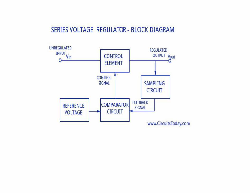
Block Diagram

Types of Voltage Regulators
• Series Voltage Regulator• Shunt Voltage Regulator

Series Voltage Regulator

Series Voltage Regulator
• A control element is placed to collect the unregulated input which controls the magnitude of the input voltage and passes it to the output.
• The output voltage is then fedback to a sampling circuit and then compared with a reference voltage and sent back to the output.
• If the output voltage tends to increase the comparator circuit provides a control signal to cause the control element to reduce the magnitude of the output voltage by passing it through the sampling circuit and comparing it, thereby maintaining a constant and steady output voltage.

Shunt Voltage Regulator

Shunt Voltage Regulator
• If the output voltage increases, the shunt current increases and thus produces less load current and maintains a regulated output voltage.
• If the output voltage reduces, the shunt current reduces and thus produces more load current and maintains a regulated constant output voltage.
IC Regulator
• IC Voltage Regulator uses integrated circuits for voltage regulation .
• One advantage of IC voltage regulator is that properties like thermal compensation, short circuit protection and surge protection can be built into the device.
• Most of the commonly used IC voltage regulators are three-terminal devices

IC Regulator

Switched Mode Power Supply
• A switched-mode power supply (SMPS) is an electronic circuit that converts power using switching devices that are turned on and off at high frequencies, and storage components such as inductors or capacitors to supply power when the switching device is in its non-conduction state.
• Switching power supplies have high efficiencies and are widely used in a variety of electronic equipment, including computers and other sensitive equipment requiring stable and efficient power supply.

Switched Mode Power Supply
Switched-mode power supplies are classified according to the type of input and output voltages. The four major categories are:
• AC to DC,DC to DC,DC to AC,AC to ACA basic isolated AC to DC switched-mode power supply
consists of:• Input rectifier and filter• Inverter consisting of switching devices such as
MOSFETs,Transformer,Output rectifier and filter• Feedback and control circuit

Switched Mode Power Supply

Switched Mode Power Supply
• The input DC supply from a rectifier or battery is fed to the inverter where it is turned on and off at high frequencies of between 20 KHz and 200 KHz by the switching MOSFET or power transistors.
• The high-frequency voltage pulses from the inverter are fed to the transformer primary winding, and the secondary AC output is rectified and smoothed to produce the required DC voltages.
• A feedback circuit monitors the output voltage and instructs the control circuit to adjust the duty cycle to maintain the output at the desired level.

Advantages and Disadvantages
Advantages of switched-mode power supplies:• Higher efficiency of 68% to 90%• Regulated and reliable outputs regardless of
variations in input supply voltage• Small size and lighter• Flexible technology• High power densityDisadvantages:• Generates EMI• Complex circuit design• Expensive compared to linear supplies

UJT relaxation oscillator
• UJT relaxation oscillator is a type of RC ( resistor-capacitor) oscillator where the active element is a UJT (uni-junction transistor).
• UJT is an excellent switch with switching times in the order of nano seconds.
• It has a negative resistance region in the characteristics and can be easily employed in relaxation oscillators.
• The UJT relaxation oscillator is called so because the timing interval is set up by the charging of a capacitor and the timing interval is ceased by the rapid discharge of the same capacitor.

UJT relaxation oscillator
UJT relaxation oscillator• When power supply is switched ON the capacitor C
starts charging through resistor R. • The capacitor keeps on charging until the voltage
across it becomes equal to 0.7V plus ηVbb. • This voltage is the peak voltage point “Vp” denoted
in the characteristics curve (Fig:2). • After this point the emitter to RB1 resistance drops
drastically and the capacitors starts discharging through this path. When the capacitor is discharged to the valley point voltage “Vv” the emitter to RB1 resistance climbs again and the capacitor starts charging. This cycle is repeated and results in a sort of sawtooth waveform across the capacitor.

UJT relaxation oscillator

A bootstrap sweep generatorA bootstrap sweep generator is a time base generator circuit whose output is fed back to the input through the feedback. This will increase or decrease the input impedance of the circuit. This process of bootstrapping is used to achieve constant charging current.Construction of Bootstrap Time Base GeneratorThe boot strap time base generator circuit consists of two transistors, Q1which acts as a switch and Q2 which acts as an emitter follower. The transistor Q1 is connected using an input capacitor CB at its base and a resistor RBthrough VCC. The collector of the transistor Q1 is connected to the base of the transistor Q2. The collector of Q2 is connected to VCC while its emitter is provided with a resistor RE across which the output is taken.

A diode D is taken whose anode is connected to VCC while cathode is connected to the capacitor C2 which is connected to the output. The cathode of diode D is also connected to a resistor R which is in turn connected to a capacitor C1. This C1 and R are connected through the base of Q2 and collector of Q1. The voltage that appears across the capacitor C1 provides the output voltage Vo.


Operation of Bootstrap Time Base GeneratorBefore the application of gating waveform at t = 0, as the transistor gets enough base drive from VCC through RB, Q1 is ON and Q2 is OFF. The capacitor C2 charges to VCC through the diode D. Then a negative trigger pulse from the gating waveform of a Monostable Multivibrator is applied at the base of Q1 which turns Q1 OFF. The capacitor C2 now discharges and the capacitor C1 charges through the resistor R. As the capacitor C2 has large value of capacitance, its voltage levels (charge and discharge) vary at a slower rate. Hence it discharges slowly and maintains a nearly constant value during the ramp generation at the output of Q2.


Current Time Base Generators
• The generator which generates a waveform which is responsible for the movement of spot on screen horizontally is called time base generator or sweep generator.
• The sweep circuit along with the display gating functions is called time bases.
• The linear sweep moves the spot from left to right while the movement of spot from right to left is not visible.

This portion of waveform generated by time base is called flyback or retrace. During this time, the cathode ray tube is blanked.The time base generator also controls the rate at which the spot moves, across the screen.This rate is to be adjusted from front panel control.

Current Time Base Generators
• When switch S1 is closed, S2 is open and capacitor charges to produce linear ramp at the output.
• The sweep rate can be controlled by changing the value of capacitor or charging current.
• Reaching to the maximum value of ramp voltage, the switch S2 is closed and S1 is open.
• Thus capacitor gets discharged through the resistance R. this is called flyback or retrace.

The time t1 is called sweep time. The circuit is a sort of relaxation oscillator which generates saw tooth waveform. But this circuit has less accuracy. The bootstrap techniques allow much greater linearity but he techniques are much more costly.