boost power factor corrector design with the uc3853
TRANSCRIPT

BOOST POWER FACTOR CORRECTORDESIGN WITH THE UC3853
APPLICATION NOTE U-159
Phillip C. Todd

BOOST POWER FACTOR CORRECTOR DESIGN WITH THE UC3853
by Philip C. Todd
U-159UNITRODE CORPORATION
ABSTRACT
The UC3853 is designed to provide high performance power factor correction (PFC) for low to mediumpower applications with minimal complexity. It provides power supplies in the range of 10 to 200 watts witha low distortion, power factor corrected input current, a regulated output voltage and operation over a widerange of input voltages. The UC3853 uses average current mode control and works with either a boost orflyback converter. It was developed from the UC3854 family of PFC control circuits and has the same func-tionality in an 8-pin package. Much of the information available for the UC3854 family of integrated circuitsis also applicable to the UC3853. In particular, Unitrode Application Note U-134 provides a good generalintroduction to power factor correction. U-134 contains an extended description of power factor correction,the boost PFC and the control circuits necessary to provide the correct programming of the current wave-form. The reader is urged to review that note as well as this one before designing a boost power factor cor-rector.
This Application Note describes the features and functions of the UC3853 in detail. The design process fora boost power factor corrector is presented and the design details for a 100W output boost power factorcorrector with a “universal” input voltage range of 80-270VAC are included. A table that extends the 100Wboost converter example over the range of 25W to 200W is featured. A step-by-step summary of the designprocess is also provided so that the boost converter circuit may be customized for any application.
ABOUT THE UC3853 PFC CONTROLLER
The UC3853 has many similarities to the UC3854based family of devices. It contains an average cur-rent mode control loop for a low distortion input cur-rent waveform, a multiplier to program an accuratecurrent waveform and a voltage error amplifier toregulate the output voltage. The UC3853 also con-tains over-voltage protection for the output and hasa fixed frequency internal oscillator which is syn-chronizable.
A block diagram of the UC3853 is shown in Figure1. Due to its 8-pin simplicity, some pins serve morethan one function and some functions are broughtinside the chip altogether. The UC3853 beginsoperation when the voltage at the VCC pin isgreater than 11.5V. An undervoltage lockout func-tion (UVLO) keeps the device from operatingbefore this voltage is reached. The UC3853 entersthe UVLO state again when VCC drops below 9.5V.The hysteresis in the UVLO allows the device to bestarted from a capacitor which is trickle chargeddirectly from the input voltage.When in UVLO, most
of the internal circuits are not powered so the sup-ply current is less than 500µA (250µA typical). Thereference voltage in the UC3853 is internal to thedevice and is not brought out to a pin. The refer-ence is divided down to 3.0V at the non-invertinginput to the voltage error amplifier. The reference istrimmed to an accuracy of better than 2% at the FBpin of the voltage error amplifier so the referencevoltage specification includes the offset of theamplifier. The total variation of the reference overtemperature, including the set point accuracy, is3.0V ±3.5%. For a typical 400V output the accura-cy translates into an output variation of ±8V at roomtemperature, which is comparable to the ripple volt-age amplitude on the output at full power.
The output of the UC3853 supplies 500mA peakcurrent to the gate of the power MOSFET switch. Asimplified schematic of the output driver is shown inFigure 2. The VCC pin provides the voltage feed-forward signal needed by the multiplier/divider/squarer circuit and thus it has a wide input voltagerange under normal operation. The output voltage

U-159APPLICATION NOTE
2
is therefore clamped near 15V to prevent the gateof the MOSFET switch from being driven beyondits breakdown voltage as VCC changes. Whenpower is not applied to the device the output driveris self-biased to hold the output to within 1.5V ofground. When VCC is above the UVLO thresholdthe bias circuit is disabled and the output driveroperates normally.This prevents the MOSFET fromturning on when power is first applied to the con-verter. If the output were not held low, the gate todrain capacitance of the MOSFET would pull thegate high when power is applied and turn thedevice on, which often results in its destruction.
The PWM comparator uses the oscillator ramp andthe output of the current amplifier to generate the
gate drive output as shown in Figure 3. The outputof the comparator is latched for the duration of theclock period to prevent false output pulses. Thelatch is set by the clock signal at the beginning ofeach clock period to drive the output high and isreset by the PWM comparator to drive the outputlow. The output is kept low by the status inputs tothe AND gate that drives the output. The statusinputs are the undervoltage lockout (UVLO), thereference valid and the output overvoltage statussignal. The output is also held low during the clockinterval.
The oscillator is internal to the UC3853, has a fixed75kHz operating frequency and may be synchro-nized to an external source. The oscillator wave-form is a reverse sawtooth because a negativeslope ramp is required to provide the proper polar-ity for the PWM circuit and for the slope compen-sation of the average current loop. The current looperror amplifier inverts the current signal so theoscillator ramp must have a negative slope. The rel-
Figure 1. Block Diagram of UC3853
Figure 2. UC3853 Output Driver (Simplified Schematic) Figure 3. UC3853 PMW Circuit
UDG-96250
UDG-96251 UDG-96252

U-159APPLICATION NOTE
3
ative polarity of the two signals is therefore oppo-site, which is the correct orientation.This is all inter-nal to the device. The width of the clock outputpulse determines the minimum dead time of theoutput and is less than 1% of the clock period. Anequivalent circuit for the oscillator and the sync cir-cuit is shown in Figure 4.
The synchronizing pulse for the oscillator comesfrom the FB pin. The voltage feedback and theovervoltage protection are also connected to theFB pin. If the synchronizing signal is capacitivelycoupled into the FB pin it will not upset the DC out-put voltage value since the bandwidth of the ampli-fier is very small compared to the switching fre-quency. The compensation network on the outputof the transconductance amplifier will eliminate thesynchronizing signal from the output of the amplifi-er. The guaranteed synchronization frequencyrange is 95kHz to 115kHz. Circuits for synchroniz-ing the oscillator are described later in thisApplication Note.
The voltage and current loop amplifiers, the squar-er and the multiplier/divider circuits are shown inFigure 5. The current amplifier is a wideband oper-ational amplifier and it has ground referencedinputs. The inverting input of the amplifier is a sum-ming junction where the feedback, the input currentsignal and the current programming signal from themultiplier output come together. The current signalis negative and the output of the multiplier is posi-tive so the current loop is adjusted to keep the volt-age at the inverting input zero since the non-invert-
ing input of the current amplifier is connected toground through a 3.9kΩ resistor. This resistor pro-vides DC balancing of the amplifier input bias cur-rents. The amplifier has sufficient output drivecapability to handle a wide range of feedback net-works.
The squarer and multiplier/divider are the heart ofthe control circuit and are shown in Figure 5. Thiscircuitry makes it possible to operate a boost PFCstage over a 3:1 input voltage range and still getexcellent voltage loop bandwidth and fast responseto input voltage variations. The multiplier/dividerrequires three inputs which are traditionally labeledA, B and C. The A input is the output of the voltageerror amplifier which controls the average outputvoltage.The B input is the IAC signal which is a cur-rent from the input voltage and it is multiplied by theoutput of the voltage error amplifier to provide thecurrent shape and amplitude needed to programthe current loop.The C input is the divider input andit is the feed forward voltage that comes throughthe squarer. This input is proportional to the squareof the average input voltage and it adjusts the gainof the multiplier to keep the gain of the voltage con-trol loop constant. This is the secret to achieving awide bandwidth control loop over a wide input volt-age range. The squaring circuit takes its input fromthe VCC pin so the bias voltage for the UC3853must be proportional to the input voltage for thisfeature to work properly.
The voltage error amplifier in the UC3853 is atransconductance amplifier and it has both a high
Figure 4. UC3853 Oscillator Equivalent Circuit
UDG-96253

4
U-159APPLICATION NOTE
input impedance and a high output impedance,which is a controlled current source output ratherthan the usual low impedance voltage source out-put.The gain of a transconductance amplifier is notgiven by the ratio of volts out to volts in. Instead itis given by the ratio of amperes out to volts in,which is a transconductance (the inverse of aresistance) and has the units of Siemens. Thetransconductance is a gain in this case and is oftendenoted by the symbol GM. The gain of atransconductance amplifier can be changed into avoltage ratio by multiplying the transconductancegain by the load resistance. Hence, the voltagegain is set by an RC network to ground from theoutput of the amplifier. This allows the gain and fre-quency response of the amplifier to be determinedby the load impedance without any componentsconnected from the output of the amplifier to theinput.
A transconductance amplifier was chosen to allowthree functions to be combined on the FB pin. Theoscillator sync input and the overvoltage compara-tor share the same input pin as the error amplifierso if a feedback network were connected aroundthe amplifier the overvoltage comparator would beinaccurate. Since both the transconductanceamplifier and the overvoltage comparator requireonly a simple voltage divider at their inputs forproper operation they can be combined into a sin-gle pin. The non-inverting input of the voltageamplifier is connected to a 3.0V DC referencewhich is the reference for the output voltage. Theovervoltage comparator turns the output of theUC3853 off when the voltage at the FB pinexceeds 3.15V. The output turns back on when thevoltage at the FB pin comes back to 3.0V.
BOOST PFC POWER STAGE DESIGN WITHTHE UC3853
The circuit for a boost PFC is shown in Figure 6.The reference designators for the parts on theschematic match those in U-134 where the func-tions of the parts are the same. In all cases the ref-erence designators are appropriate for the functionof the device. A 100W boost power factor correctoris used as an example of the design process andthis is the circuit that is shown in Figure 6. A tableis provided at the end of this Application Note thatextends the design over the range of 25W to200W. The control circuits are the same whether at25W or at 200W. The values of the control circuitcomponents change only if the choices for circuitperformance are different from those made here.The following design process allows the design tobe modified to suit a wide variety of applications.
The design of a boost PFC begins with the specifi-cation for the system performance. The minimumand maximum input line voltages, the maximumoutput power, and the line frequency range mustbe specified. For the example circuit the specifica-tions are:
• Maximum power output: 100 Watts• Input line voltage range: 80-270VAC• Line frequency range: 47-65Hz
The input line voltage and frequency range are a“universal” input range and allow this power factorcorrector to operate from power lines anywhere inthe world without switches or other adjustments.
The output voltage needs to be at least 5% higherthan the peak voltage of the highest input line volt-age. The peak of a 270VAC line will be about 380V
Figure 5. UC3853 Error Amplifiers, OVP Comparator and Multiplier, Divider, Squarer
UDG-96254

U-159APPLICATION NOTE
so 400V is chosen as the DC output voltage.
The switching frequency is an important considera-tion in the design process and the switching fre-quency is internally fixed in the UC3853 at 75kHznominal and may be synchronized to an external100kHz oscillator.
INDUCTOR SELECTION
The peak current that the inductor must carry is thepeak line current at the lowest input voltage plusthe peak high frequency ripple current. The peakline current is given by the following equation:
lLINEpk =
Where P is the maximum input power to the con-verter. Generally, using the output power is suffi-ciently accurate for this calculation since the effi-ciency of the converter should be greater than90%. If greater accuracy in the design process isrequired, the design may be completed, the effi-ciency calculated and then the design process maybe iterated using the calculated value for efficiency.For the example converter, the output power is100W and VINmin is 80VAC so ILINEpk is 1.77A.
2 • P
VINmin
5
The high frequency ripple current, ∆Ι, must be keptreasonably small and is usually in the range of 15%to 25% of the peak line current given above. If theripple current is too high the AC input filtersrequired to filter out this noise become larger. If theripple current is too low the value of the inductanceis too large and the cusp distortion on the leadingedge of the waveform will be large and the powerfactor will be low. For the example converter, theripple current, ∆Ι, is chosen to be 20% of the peakline current or about 0.35A peak-to-peak. The peakcurrent in the inductor, ΙLpk, is the sum of the peakline current and half of the peak-to-peak ripple cur-rent or 1.95A for the example converter.
The value of the inductor is determined by the peakcurrent at low input line voltage, the duty factor, D,at that input voltage and the switching frequency.This value of the duty factor is given by the follow-ing equation:
D =
Where VINmin is the minimum RMS input line volt-age and VO is the DC output voltage. For the exam-ple converter VINmin is 80V and VO is 400V so D is0.72.
VO - 2 • VINmin
VO
Figure 6. Schematic of a Boost Power Factor Corrector Using the UC3853
UDG-96255
U-159APPLICATION NOTE
The value of the inductor is given by the followingequation:
L =
Where VINmin is the minimum RMS input voltageand D is given from the equation above.The switch-ing frequency is fs and ∆Ι is the maximum peak-to-peak ripple current. For the example converter VINis 80V, D is 0.72, fs is 75kHz and ∆Ι is 0.35A peak-to-peak as determined above. This gives an induc-tance of 3.1mH. A value of 3.0mH nominal will beused.
Note that the ripple current changes with input volt-age so it varies as the line voltage goes through itscycle. Under normal operation the ripple currentcan be significantly greater than the 20% specifiedhere. The maximum ripple current occurs when themomentary value of the input voltage equals halfthe DC output voltage which corresponds to 50%duty ratio.
OUTPUT CAPACITOR SELECTION
CO, the output capacitor generally falls in the rangeof 1 to 2µF per watt for typical 400V output appli-cations. Since low cost is one of the targets of thisconverter, 1µF/W is chosen and thus a 100µFcapacitor will be used for CO. There are many fac-tors that influence the value of the output capacitor.The output voltage hold-up time, the output ripplevoltage, the loop transient response and the inputcurrent third harmonic distortion are all dependentto some degree on the value of the output capaci-tor and, in all cases except cost, a larger value ofthe output capacitance results in better perfor-mance. Nevertheless, a reasonable compromisecan be reached with the 1µF/W value.
All power factor correction circuits have a large rip-ple current on their output at the second harmonicof the line current as highlighted in U-134. As theoutput capacitor becomes smaller, the output ripplevoltage due to the second harmonic ripple currentincreases and the bandwidth of the voltage loopmust be made smaller to keep the same level ofdistortion in the input current. A 1% second har-monic ripple voltage at the output of the voltageerror amplifier becomes 0.5% third harmonic dis-tortion of the input current. The only ways to reducethis source of distortion are to (1) increase the sizeof the output capacitor and (2) reduce the gain ofthe error amplifier at the second harmonic frequen-cy by reducing the amplifier bandwidth. Reducingthe loop bandwidth slows the transient responseand increases its deviation.
The output capacitor may need to be larger forother reasons. If hold-up time is required, the
2 • VINmin • D
∆l • fS
6
capacitor may need to be larger than 1µF/W. Thefollowing equation may be used to calculate thesize of the capacitor for a given hold-up time, poweroutput and voltage change.
CO =
Where P is the rated power of the converter, ∆t isthe required hold-up time, VO is the DC output volt-age of the converter and VOmin is the voltage towhich the output decays at the end of the hold-uptime. For the example converter, 100µF gives about19 milliseconds of hold-up time for a 50V change inVO or 35 milliseconds of hold-up for a 100Vchange.
CURRENT SENSE RESISTOR
RS, the current sense resistor, is selected to pro-vide 1.0V at the maximum current expected in theinductor. ILINEpk plus half the peak-to-peak ripplecurrent is the peak current through the inductor andwas calculated above. The value of the currentsense resistor is found from: 1.0V/ILpk. For theexample converter the peak current in the inductoris 2.0A maximum so the value of the sense resistoris 0.5Ω.
SWITCHES AND DIODES
The power switch must have a low RDSon ratingand a peak voltage rating greater than the outputvoltage of the converter with some margin for tran-sient overshoot, ripple voltage on the output andappropriate levels of derating. A low RDSon of thepower switch will result in lower conduction lossesbut these devices also have high gate capacitancesand may therefore have longer turn-on times,resulting in greater overall switch power dissipation.There is an optimum size switch for each applica-tion although the optima is rather broad.Suggestions for switches for a variety of power lev-els are contained in the table at the end of thisapplication note. These are by no means the onlypossibilities and are simply generic choices. For theexample converter an IRF830 was chosen.
The output diode must be rated for the peak outputcurrent and must be an incredibly fast diode. Areverse recovery time below 100 nanoseconds isstrongly recommended and faster is much better.The reverse recovery time of the diode has a directeffect on the power dissipation in the switch. Theswitch must conduct full output current at full outputvoltage from the time it turns on until the diodeturns off. For the example converter this will be400V at 2.0A for a peak power of 800W. If this lastsfor 100nsec the average power will be 6.0W at a75kHz switching frequency. If a 35nsec recovery
2 • P • ∆tVO2 - VOmin2

U-159APPLICATION NOTE
7
diode is used the average power will be 2.1W.There are many diodes available that meet therequirements of this application. The temperaturerise of the diode must be kept below maximum forthe worst case conditions as well. The reverserecovery time of the diode becomes larger as thetemperature increases and this increases thepower dissipation of the switching transistor. Heatsinking of the diode may be required to control themaximum temperature. For the example convertereither an MUR460 or a BYM26C is used.
INPUT DIODES
The input diodes are not particularly critical. Theymust have a current rating sufficient for the maxi-mum current at low line and they must be held to areasonable temperature rise. Fast recovery typesgenerally prove to be a bit less noisy than standardrecovery types. Avalanche breakdown types workbetter with noisy power lines. The exact choice ofinput diodes depends on many such factors as wellas the amount of filtering present on the AC side ofthe bridge. For the example converter, MR856 orBYW95C diodes are used. Both are fast recoverytypes.
CIN is part of the input filter even though it is afterthe input diodes. The value must be chosen in con-junction with the input filter and must be kept rea-sonably small. This capacitor carries most of theripple current from the inductor so it needs to be afilm type capacitor with a substantial high frequen-cy ripple current capability. At light loads CIN canhave a large effect on the distortion of the input cur-rent because it is after the input diodes. At theselow currents, especially near the input voltage zerocrossing, the capacitor stores enough energy tomaintain the output current and the input diodesturn off, thus introducing distortion into the inputcurrent. For the example converter, a 1.0µF capac-itor was chosen to give less than 1V peak-to-peakripple voltage at the switching frequency with 100Woutput.
CONTROL CIRCUIT DESIGN WITH THE UC3853
The heart of the UC3853 is the multiplier and it isquite easy to set the parameters for proper opera-tion. The equation for the multiplier is given belowand, even though it looks complex, it is quitestraight forward.
IMO =IAC • (VCOMP - 1.5)
KM • 5555
IMO is the output current from the multiplier. IAC isthe programming current that comes from the inputthrough RAC and is proportional to the input volt-age. It tells the current loop what to do to maintainan input current which is proportional to the inputvoltage. VCOMP is the output of the voltage erroramplifier and is the other input to the multiplier. KMis the gain constant of the multiplier and is given inthe data sheet for the UC3853. VCC is the supplyvoltage to the UC3853 and it is divided by eightinternally and then squared in the squaring circuit.This forms the divider input to the multiplier and isused to keep the gain of the voltage loop constantso that the loop bandwidth may be kept large andthus have a relatively fast transient response.
IAC must be programmed to have a maximum valueof 500µA when the AC line voltage is at its peak.The voltage at the IAC pin is 2.0V so it introducesvery little error into the current if this voltage isignored. For the example converter the maximuminput voltage is 270VAC and this has a peak valueof about 380V. A 760kΩ resistor will give 500µA.Most resistors are only rated to 250V so two resis-tors will be needed in series. The closest standardvalue is 390kΩ so this value is chosen for bothRAC1 and RAC2.
CURRENT LOOP COMPENSATION
The peak value of IMO is about 250µA with the val-ues of RAC given above. If RMO is made 3.9kΩ, thepeak value of voltage across RS will be 1.0V. Thisvalue of RMO also matches the 3.9kΩ resistor inter-nal to the UC3853 which is connected to groundfrom the non-inverting input of the current erroramplifier. These two values provide the correct bal-ance for the DC bias currents into the amplifier andgive the correct input offset voltage. If the offsetvoltage is in the wrong direction the current loopcould latch at zero output.
The PFC input current must track the current pro-gramming signal (IMO) from the multiplier veryclosely to achieve a low distortion input current.Accurate tracking requires high gain in the currentloop to minimize the errors. For the current loop tobe stable, the frequency at which the gain of theloop is equal to one must be less than one thirds ofthe switching frequency and the gain must roll offwith a single pole slope.The boost power stage hasa single pole due to the main inductor and the cur-rent sense resistor. This L/R pole creates a stableloop with a fixed gain, wide bandwidth error ampli-fier. These two requirements can be accommodat-ed by using pole zero compensation around theerror amplifier. Pole zero compensation has high
VCC8
2( )
U-159APPLICATION NOTE
8
gain at low frequencies and flat gain at high fre-quencies so that the input current tracks the pro-gramming signal accurately and is also stable athigh frequencies. This is the essence of averagecurrent mode control and it is necessary for a lowdistortion PFC.
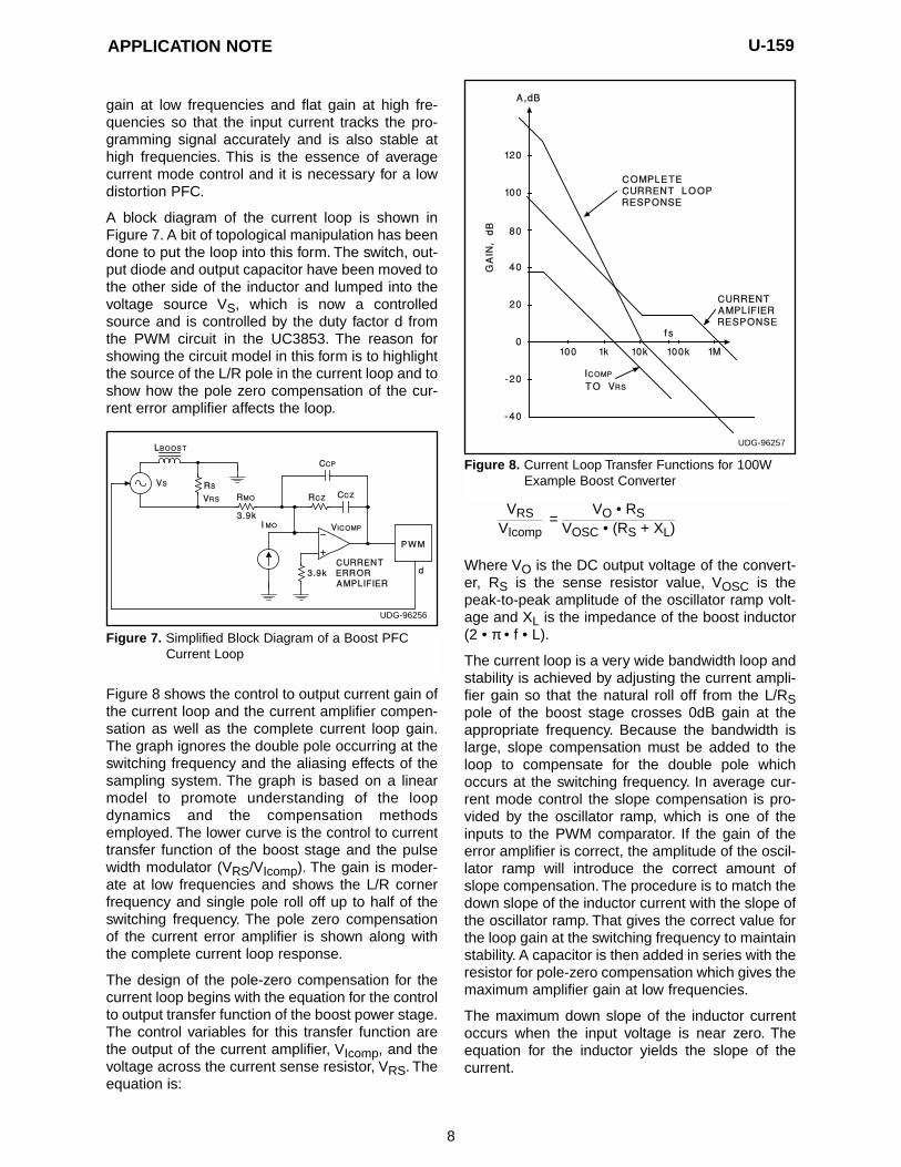
A block diagram of the current loop is shown inFigure 7. A bit of topological manipulation has beendone to put the loop into this form. The switch, out-put diode and output capacitor have been moved tothe other side of the inductor and lumped into thevoltage source VS, which is now a controlledsource and is controlled by the duty factor d fromthe PWM circuit in the UC3853. The reason forshowing the circuit model in this form is to highlightthe source of the L/R pole in the current loop and toshow how the pole zero compensation of the cur-rent error amplifier affects the loop.
Figure 8 shows the control to output current gain ofthe current loop and the current amplifier compen-sation as well as the complete current loop gain.The graph ignores the double pole occurring at theswitching frequency and the aliasing effects of thesampling system. The graph is based on a linearmodel to promote understanding of the loopdynamics and the compensation methodsemployed. The lower curve is the control to currenttransfer function of the boost stage and the pulsewidth modulator (VRS/VIcomp). The gain is moder-ate at low frequencies and shows the L/R cornerfrequency and single pole roll off up to half of theswitching frequency. The pole zero compensationof the current error amplifier is shown along withthe complete current loop response.
The design of the pole-zero compensation for thecurrent loop begins with the equation for the controlto output transfer function of the boost power stage.The control variables for this transfer function arethe output of the current amplifier, VIcomp, and thevoltage across the current sense resistor, VRS. Theequation is:
=
Where VO is the DC output voltage of the convert-er, RS is the sense resistor value, VOSC is thepeak-to-peak amplitude of the oscillator ramp volt-age and XL is the impedance of the boost inductor (2 • π • f • L).
The current loop is a very wide bandwidth loop andstability is achieved by adjusting the current ampli-fier gain so that the natural roll off from the L/RSpole of the boost stage crosses 0dB gain at theappropriate frequency. Because the bandwidth islarge, slope compensation must be added to theloop to compensate for the double pole whichoccurs at the switching frequency. In average cur-rent mode control the slope compensation is pro-vided by the oscillator ramp, which is one of theinputs to the PWM comparator. If the gain of theerror amplifier is correct, the amplitude of the oscil-lator ramp will introduce the correct amount ofslope compensation. The procedure is to match thedown slope of the inductor current with the slope ofthe oscillator ramp. That gives the correct value forthe loop gain at the switching frequency to maintainstability. A capacitor is then added in series with theresistor for pole-zero compensation which gives themaximum amplifier gain at low frequencies.
The maximum down slope of the inductor currentoccurs when the input voltage is near zero. Theequation for the inductor yields the slope of thecurrent.
VO • RSVOSC • (RS + XL)
VRSVIcomp
Figure 8. Current Loop Transfer Functions for 100WExample Boost Converter
Figure 7. Simplified Block Diagram of a Boost PFCCurrent Loop
UDG-96256
UDG-96257

U-159APPLICATION NOTE
9
=
Where dI/dt is the slope of the inductor current inamperes per second, VO is the DC output voltageof the converter and L is the value of the boostinductance. This current flows through the senseresistor and becomes a voltage so the equation ismodified as follows:
= • RS
Where RS is the sense resistor value. For theexample converter the output voltage is 400VDCand the inductance is 3.0mH so the dI/dt is0.133A/µsec, and RS is 0.5Ω so dV/dt is0.066V/µsec.
The oscillator in the UC3853 has a peak-to-peakamplitude of 5.0V and the period is 13.3µsec so theslope is 0.375V/µsec (the slope does not changewith synchronization). The gain of the currentamplifier at the switching frequency is determinedby the ratio of the oscillator voltage slope divided bythe current slope. The gain of the current amplifierat the switching frequency is the ratio of RCZ toRMO. For the example converter the current slopeis 0.066V/µsec and the oscillator slope is0.375V/µsec so the gain is 5.625. RMO is 3.9kΩ soRCZ is 22kΩ.
The value of the capacitor CCZ, which introduces azero into the current error amplifier response, is setby the current loop crossover frequency. The zeromust be at or below that frequency to maintain thephase margin of the current loop. The equation forfCI given below is simplified somewhat but is accu-rate over this frequency range.
fCI =
Where VO is the DC output voltage of the convert-er, RS is the value of the current sense resistor andRCZ is the current amplifier feedback resistancedetermined above. VOSC is the peak-to-peak oscil-lator ramp voltage, L is the value of the boost induc-tor and RMO is the current amplifier input resis-tance. For the example converter, VO is 400VDC,RS is 0.5Ω, RCZ is 22kΩ, VOSC is 5V, L is 3.0mHand RMO is 3.9kΩ resulting in an fCI of 12kHz.
CCZ must have an impedance equal to or less thanRCZ at fCI. This is easily found from:
CCZ =
For the example converter, fCI is 12kHz and RCZ is22kΩ so CCZ must be greater than 600pF. A 680pF
12 • π • fCI • RCZ
VO • RS • RCZ2 • π • L • RMO • VOSC
VO
L
dV
dt
VO
L
dl
dt
capacitor is chosen to give a bit of extra phasemargin.
CCP is included to suppress high frequency noisein the current amplifier and it must have an imped-ance of at least 2 • RCZ at the switching frequency.Substituting fS for fCI into the equation above givesCCP.
CCP =
For the example converter CCP must be less than50pF. A value of 33pF is chosen to accommodate a100kHz synchronization frequency.
A hard current limit is not necessary to protect theswitch in an average current mode controlled sys-tem. The gain of the current amplifier is set so thatthe maximum change of current in the inductorresults in at most a 20% change of the current dur-ing one clock period. This makes it impossible forthe control circuit to cause the switch to be on longenough to enter an overcurrent condition. The cur-rent programming signal is also limited so theinductor current can not exceed this value.
HARMONIC DISTORTION BUDGET
Once the current loop is stable the next two tasksare setting the voltage loop compensation and thefeedforward compensation. Both of these are deter-mined by the amount of harmonic distortion eachcontributes to the input current. The voltage loopcontributes 0.5% third harmonic distortion to theinput current for each 1% ripple voltage at the out-put of the error amplifier. The feedforward compen-sation comes from the voltage supplied to theUC3853 and each 1% ripple on this input con-tributes 1% third harmonic distortion to the inputcurrent.
The choice of input current harmonic distortion limitand the allocation of this distortion to the two majorsources is somewhat arbitrary. For the exampleconverter, the THD will be limited to 5% of the inputcurrent. The voltage loop is allowed to contribute2% of the distortion and the feedforward voltage isallowed to contribute 2% of the distortion. Theremaining 1% will be allocated to other sourcessuch as cusp distortion and possible multiplier non-linearity. 5% THD gives a power factor of 0.99875.
VOLTAGE LOOP COMPENSATION
A simplified block diagram of the voltage loop isshown in Figure 9. Average current mode controlturns the power stage of the boost converter into avoltage controlled current source driving a capaci-tor, CO, in parallel with the load resistance. The cur-
1
2 • π • fS • 2 • RCZ

U-159APPLICATION NOTE
10
rent loop therefore becomes a transconductanceamplifier with a voltage input and current output.The voltage gain of the current loop is given byGCL • ZL where GCL is the transconductance of thecurrent loop and ZL is the parallel combination ofCO and RL, the load resistance. The frequencyresponse of the current loop has a DC gain givenby GCL • RL and a single pole roll off due to CO andRL within the frequency range of interest.Theoretically, if the voltage loop is closed aroundthe current loop with a fixed gain error amplifier, thevoltage loop will be stable because there is only asingle pole from CO and RL within the loop. As thegain of the amplifier increases, the bandwidth of thevoltage loop also increases. Although this solutionis very appealing, it is not feasible with the UC3853because the limited current capability of the voltageerror amplifier. Therefore, the error amplifier com-pensation will have a zero below and a pole at thecrossover frequency of the voltage loop.
The multiplier in the voltage loop adds the currentprogramming signal from the line frequency and itacts like a switching frequency. Therefore the band-width of the voltage loop must be kept below(2 • fL/π) to maintain voltage loop stability where fLis the line frequency. The gain of the error amplifierneeds to be high to maintain wide bandwidth in thevoltage loop and thus fast transient response but ifit is too high the loop will go unstable due to the linefrequency introduced by the programming signal inthe multiplier. If the gain of the amplifier in the loopis set with a fixed gain to give maximum bandwidth,the DC gain of the loop is reasonable and the out-put voltage regulation is within a percent or two ofthe set point.
The relatively wide bandwidth of the loop givesgood transient response but also gives little attenu-ation of the second harmonic ripple voltage on theoutput capacitor. This voltage modulates the input
current so the harmonic distortion of the input cur-rent will be too high. Reducing the harmonic distor-tion requires reducing the gain of the loop at thesecond harmonic of the power line frequency,which is the ripple voltage frequency on the outputcapacitor. The bandwidth of the loop must also bekept as high as possible to maintain good transientresponse. If the loop is closed with an error amplifi-er having an extra pole just after the unity gaincrossover frequency, it is possible to reduce theharmonic distortion and still maintain good loopbandwidth and adequate phase margin.
Figure 10 is a Bode diagram of the resulting loopresponse. The loop response has a pole at low fre-quency due to the load resistance and the outputcapacitance and then rolls off smoothly with a firstorder slope due to the output capacitor. Just afterthe gain of the loop crosses 0dB at fVI, a secondpole takes the slope to a second order roll off andthis reduces the loop gain to the required level atthe second harmonic of the line frequency. Forgreater DC regulation of the output voltage andbecause of the requirements of the voltage erroramplifier on the UC3853, a zero is added to theloop at low frequencies to compensate for the loadresistance and output capacitance pole.
The design of the voltage loop compensationbegins at the output capacitor. The voltage loopcompensation reduces the amplitude of the ripplevoltage from the output capacitor to a level, at theoutput of the voltage error amplifier, which is con-sistent with the harmonic distortion specification.The amount of ripple voltage on the output capaci-tor, CO, is given by the following equation.
∆VOpk =
Where P is the maximum input power of the con-verter. Use of the input power in place of the outputpower is a reasonable compromise since the effi-ciency of the converter is high. The lowest power
P
2 • π • 2 • fLmin • CO • VO
Figure 9. Simplified Block Diagram of a Boost PFCVoltage Loop
UDG-96258
Figure 10. Transfer Functions of Voltage Loop
UDG-96259

U-159APPLICATION NOTE
line frequency is fLmin, the output capacitor value isCO and VO is the DC output voltage. For the exam-ple converter, P (approximately POUT) is 100W,fLmin is 47Hz, CO is 100µF and VO is 400VDC.∆VOpk is therefore 4.2Vpk. Note that this is half thepeak-to-peak value. Mathematically, this is theamplitude of the ripple voltage vector. At low linefrequencies the ripple voltage is larger as is thegain of the error amplifier because of the loop com-pensation requirements. If performance is to bemaintained over the range of line frequencies, thenthe lowest frequency must be used for the design.
The gain of the voltage error amplifier and the volt-age divider preceding it are determined by the har-monic distortion budget for the voltage loop and theamount of ripple voltage on the output capacitor.The amount of ripple voltage allowed on the outputof the voltage error amplifier is equal to twice thepercentage of the distortion. Each 1% of secondharmonic ripple voltage on the output of the ampli-fier results in 0.5% third harmonic current on theinput. The %ripple on the output of the voltage errormust be translated into an absolute voltage to findthe gain of the voltage error amplifier and the volt-age divider at the second harmonic of the line fre-quency. The %ripple is multiplied by the range ofthe output voltage (∆VCOMP) to get the amplitudeof the ripple voltage on the output of the amplifier.This is divided by the amplitude of the ripple volt-age on the output capacitor to give the combinedgain of the voltage error amplifier and the voltagedivider. The equation for the gain is:
GV =
Where GV is the gain of the voltage divider and thevoltage error amplifier, ∆VCOMP is the range of thevoltage error amplifier output, %ripple is the per-centage of ripple voltage allowed in the output ofthe voltage error amplifier and ∆VOpk is given pre-viously. For the example converter, ∆VCOMP isactually the active range of the input to the multipli-er rather than the output range of the amplifier. Onthe UC3853 the active input range of the multiplieris between 1.5V and 6.0V so ∆VCOMP is 4.5V. Thepercent THD of the input current allowed from thevoltage loop according to the harmonic distortionbudget is 2% which results in 4% ripple voltage atthe output of the voltage error amplifier. The numer-ic value of 0.04 must be used in the equation. Thevalue of ∆VOpk is 4.2V. Therefore:
GV = = 0.043
The voltage divider is composed of RVI and RVDand is determined by the ratio of the DC output volt-age to the internal reference voltage in the
4.5 • 0.04
4.2
∆VCOMP • %ripple
∆VOpk
11
UC3853, which is 3.0V. The impedance of the volt-age divider is somewhat arbitrary. For the exampleconverter the output voltage is over 250V so tworesistors are used in series to get the necessaryvoltage rating. 1.24MΩ is chosen as the dividerimpedance so two 620kΩ resistors are used forRVI. RVD is determined from the voltage dividerequation and the value is just below 10kΩ so a10kΩ resistor is used with a 150kΩ resistor in par-allel. The gain of the voltage divider is given by thefollowing equation:
GVD =
The gain of the voltage divider, GVD, is 0.0075 inthe example.The gain of the divider and the voltageamplifier together must be 0.043. The gain of theamplifier at twice the line frequency (low line fre-quency is 47Hz) must be 5.7 for the example con-verter.
The gain of a transconductance amplifier is givenby A = GM • ZA. Where A is the voltage gain of theamplifier, GM is the transconductance of the ampli-fier and ZA is the load impedance from the VCOMPpin to ground. The transconductance of the amplifi-er in the UC3853 is 485µmhos.The gain needed forthis application is 5.7, so the load impedance is11.75kΩ. At the second harmonic of the line fre-quency, the gain of the amplifier is determined byCVC, the voltage compensation capacitor. For theexample converter, a capacitor with an impedanceof 11.75kΩ at 94Hz has a value of 0.15µF and thisis the value used.
The value of RVC is found by extrapolating from thesecond harmonic frequency back to find the fre-quency at which the gain of the voltage loop isunity, fVI. RVC is then found by writing the equationfor the gain of the loop, setting it to unity and solv-ing the resulting equation for RVC. The loop equa-tion is the product of the gain of the current loopand load impedance, GBST, the gain of the voltageamplifier, GVEA, and the voltage divider, GVD.
The gain of the boost stage is given by the follow-ing equation:
GBST =
Where P is the input power and is here taken to bethe output power because of the assumption ofhigh efficiency. XCO is the impedance of the outputcapacitor and varies with frequency. ∆VCOMP is therange of the voltage error amplifier output and isequal to 4.5V on the UC3853. VO is the DC outputvoltage. By using the output power (VO • IO) in theequation, all of the terms that are associated withthe multiplier and divider drop out of the equation.
P • XCO
∆VCOMP • VO
RVD
RVD + RVI

U-159APPLICATION NOTE
circuit to compensate the gain of the voltage loopfor changes of the input voltage as shown in Figure5. The input to the squarer and divider is the supplyvoltage to the UC3853 and is called VFF. The func-tion of the supply voltage, besides powering thechip, is to feed-forward information about the inputvoltage to the voltage loop. This means that VFFmust be proportional to the average value of theinput voltage and must also have low ripple voltagebecause 1% ripple on this voltage will create 1%harmonic distortion on the input current.
The VFF input is generated by a winding on theboost inductor that operates like a transformer.When the switch is turned on, the voltage acrossthe inductor is equal to the input voltage. This volt-age is tapped off by using an additional winding onthe inductor to supply the control circuits. The cur-rent drain of the control circuits, ICC, is typicallyabout 15mA of which 10mA are allocated to theUC3853 and 5mA are allocated to the MOSFETgate drive current. These currents are constant anddo not change appreciably with a change of thesupply voltage.
The supply voltage range of the UC3853 is greatenough to cover a 3:1 input voltage range. To pro-vide the best utilization of the VFF programmingrange the supply voltage to the UC3853 should beset to provide 10.5V when the input voltage is atlow line. If a narrower range is being used for theinput voltage than is used for this example, it maybe desirable to set the minimum voltage slightlyhigher, in the range of 12V to 15V, to provide morevoltage for the gate drive at lower line voltages andthus lower RDSon. For the example converter, aturns ratio of 10:1 on the inductor will provide thecorrect value of VFF. The minimum voltage is about10.5V, with an input line voltage of 80VAC, after allof the diode drops have been taken into account.The UVLO threshold for turning the UC3853 off is9.5V so a 10.5V minimum value of VFF leavessome margin in the design for component variation.
The diode DFF must block 80V, carry an averagecurrent of 15mA for the example converter andhave a very fast recovery time. Small 100V diodes,such as BYD71B or MUR110 are suitable devicesfor this application.
The amount of harmonic distortion allocated to theVFF input of the UC3853 is 2%, so the ripple volt-age must be held to 2% of the minimum value ofVFF. For the example converter, the minimum volt-age is 10.5V so the allowable ripple voltage is0.21V. This is not the peak-to-peak value of the rip-ple but is the peak value of the second harmonic ofthe line frequency. The peak-to-peak ripple voltage,∆VFF, is this value multiplied by π. For the exampleconverter, ∆VFF is therefore 0.66V peak-to-peak.
12
The gain of the voltage divider, GVD, is givenabove. The gain of the transconductance amplifierand its load are given by the following:
GVEA = GM • XCVC
Where GM is the transconductance of the amplifierand XCVC is the impedance of the compensationcapacitor CVC.
Finally, the equation for the loop can be writtenfrom these equations as:
GV =
By setting GV = 1 the equation can be solved forfrequency since all other variables are known atthis point. Note that there are two terms in theequation which vary with frequency, XCO andXCVC. The loop has a second order roll off at thispoint so the equation is solved for the square of thefrequency. The unity gain crossover frequency, fVI,is found from the following equation.
fVI2 =
For the example converter fVI is 18.6Hz. The valueof RVC, which is what we have been trying to deter-mine all along, is equal to the impedance of CVC atfVI. For the example converter, this is 57kΩ, so a56kΩ standard value resistor is chosen.
The last step is the addition of a low frequency zeroin the feedback loop. It is accomplished by addingCVCZ in series with RVC as shown in the schemat-ic. From an operational standpoint, the effect ofCVCZ is to double the peak-to-peak variation of theoutput voltage during a step load transient. Theovervoltage protection circuit built into the UC3853will prevent the output voltage from exceeding themaximum value by turning the switch off until theoutput voltage is back within range. The undervolt-age transient caused by a step load change will beunaffected.
The value of CVCZ is not especially critical.However, since it adds both a pole and an zero tothe loop gain, the zero must be far enough away infrequency from the CVC and RVC pole so that itdoes not contribute extra phase shift at the unitygain frequency, fVI. This requires that the zero be atleast two octaves below fVI. For the example con-verter, the zero has been placed almost a fulldecade below fVI and the value of CVCZ is chosenas 1.0µF.
THE FEEDFORWARD VOLTAGE AND STARTUPCIRCUIT
The UC3853 makes use of a divider and squaring
P • GM • GVD
(2 • π)2 • CO • CVC • ∆VCOMP • VO
P • XCO • GM • XCVC • GVD
∆VCOMP • VO
U-159APPLICATION NOTE
The value of CFF can be found from the equationfor a capacitor and the current drain of the controlcircuits, ICC.
CFF =
Where CFF is the value of the VFF bypass capaci-tor, ICC is the current drain of the control circuits,∆VFF is the peak-to-peak ripple voltage on VFF andfLmin is the minimum line frequency. For the exam-ple converter the value is 240µF. A standard valueof 270µF is chosen and it is bypassed with a 0.1µFceramic capacitor.
This value for CFF also gives sufficient time to startthe circuit since one half cycle of the input line fre-quency is needed to reach full operation. The turn-on threshold of the UC3853 is 11.5V and the turn-off threshold is 9.5V so there is more than sufficientenergy stored to begin circuit operation.
∆t =
Where ∆t is the amount of time available for start-up, CFF is the capacitance on VFF, VTN is the turnon threshold of the UC3853 (11.5V), VTF is the turnoff threshold (9.5V), and ICC is the current drain ofthe control circuits. For the example converter ∆t is36 milliseconds.
Startup of the UC3853 is accomplished by charg-ing VFF to 11.5V through RB. The value of RB mustbe small enough to provide a reasonably shortturn-on delay after power is applied and yet largeenough to keep power dissipation low. The currentthrough RB at VINmin must also be greater than theUC3853 startup current (500µA). For the exampleconverter a 1 second delay at turn-on requires abias current of approximately 3mA from the lowinput line voltage. The equivalent resistance isabout 36kΩ. This resistance needs to be split intotwo equal resistors since the peak input voltage willexceed 250V so two 18kΩ resistors are used. Athigh line this gives about 6.8mA of bias current toVFF. This is less than the current required by theUC3853 so this value of RB is acceptable. If thecurrent at high line were too great, VFF would notaccurately reflect the input voltage and perfor-mance would suffer. A larger value of RB resultingin a longer turn-on delay is required in that case. Athigh line each of the 18kΩ resistors dissipates0.82W. A 2W rating is specified.
The gate drive voltage of the UC3853 is limited to15V by an internal clamp. This allows VFF tochange without causing the gate voltage to exceedthe rating of the MOSFET. The UC3853 is designedto drive moderate size MOSFET switches, and thegate drive current is limited to 500mA(pk). This is
CFF • (VTN - VTF)
ICC
ICC
∆VFF • 2 • fLmin
13
more than sufficient to obtain the fast rise and falltimes needed for high efficiency. RQ is the resistorin series with the gate of the MOSFET. Its value of33Ω is chosen to limit the peak gate current toabout 350mA under normal operating conditions. Inaddition, this is the minimum value for which DQ,the gate drive clamp, is NOT required under mostcircumstances. In general, if RQ is made smallthere will not be sufficient damping of the reso-nance of the parasitic circuit inductances with theMOSFET gate capacitance, so the output of theUC3853 could be drawn below ground. Keeping RQin the range of 30Ω to 60Ω prevents this, eliminatesthe need for DQ and at the same time providesample output current for fast rise and fall times onthe drain of the MOSFET. It is wise practice to leaveroom for DQ on the circuit board until it can be ver-ified in the laboratory that it is not needed.
OVER CURRENT PROTECTION
The boost converter is inherently unprotectedagainst any overload situation. Because the switchis connected in parallel with the input source, theDC current path through the inductor, diode and theload impedance (parallel combination of CO andRL) can not be interrupted. The result is practicallyunlimited current flowing from the input to the out-put of the converter when the output voltage fallsbelow the input voltage. This happens everyinstance when power is being applied to the con-verter at startup and when the load requires morepower than the circuit was originally designed for.Unfortunately, these situations can not be avoided,but there are certain measures which can protectthe circuit from a catastrophic failure.
The diode, DBP in Figure 6 provides protection forthe boost inductor and for the output rectifier,DOUT. During the initial charging of the outputcapacitor at startup and in case of an overload, ahigh surge current flows from the input to the out-put of the converter. This high peak current wouldflow through the boost inductor and the very sensi-tive high speed epitaxial diode used for rectifica-tion. This high surge current can saturate the induc-tor and damage the diode causing a disastrous fail-ure eventually. DBP prevents the high current flow-ing in the inductor-diode path by providing a lowerimpedance direct path between the input and theoutput. The additional benefit of the DBP diode isthe protection against input voltage transients.When other high power loads are connected to thesame distribution branch of the power line, theirturn off generates huge inductive spikes appearingat the input of the power factor corrector power sup-ply. This can cause the input voltage of the boostconverter to be higher than its output voltage evenunder normal operating conditions. The voltage

U-159APPLICATION NOTE
spikes impose an increased voltage stress on theinput rectifier diodes and it might cause the boostinductor to saturate depending on the duration andthe amplitude of the line transient. The addition ofthe DBP diode clamps the input voltage to the out-put capacitor voltage which will also absorb thetransient energies without passing high currentthrough the boost inductor and rectifier diode.
In normal circumstances DBP has no effect on thecircuit operation. Note that the diode DBP can notprevent the circuit from developing high currentsfrom the input to the output. It simply provides asafe passage for the high current to pass throughthe circuit. Once the high current is flowing, it has togo through the current sense resistor, RS. Higherthan nominal currents will develop negative voltageacross RS in excess of the 1V maximum valueused in the design. Since the IMO current is limitedto 0.5 • IAC, the IMO pin of the UC3853 will bepulled below ground. This could present a problemfor the integrated circuit because of reverse biasingthe substrate. When the IMO pin is pulled 0.3Vbelow ground (to -0.3V), the OUT pin goes highturning on the main switch of the boost converter.Since the current can not be limited, the only wayto avoid the parasitic turn on of the output is to limitthe negative voltage on the IMO pin of the IC. It isaccomplished by the Schottky diode, DMO con-nected between the IMO pin of the UC3853 and cir-cuit ground, as shown in Figure 6.
ABOUT SYNCHRONIZATION
Synchronization of the UC3853 oscillator requiresa fast falling edge on the FB pin. The minimumrequirements for the falling edge of the waveformare that it must have a slope of at least 20V/µsecand an amplitude of at least 1.0V. Faster fall timesand greater amplitudes are strongly recommended.The amplitude of the sync signal must be keptbelow 3.0V so that the FB pin is not driven belowground. The sync signal must be capacitively cou-pled into the FB pin so that the DC feedback is notdisturbed by the synchronization. The capacitormust be large enough so that it does not gainenough voltage during the pulse to trip the over-voltage comparator of the UC3853 on the risingedge of the sync waveform. These requirementsare easily met with the circuit of Figure 11 asshown below.
In most applications the UC3853 will be synchro-nized to another PWM integrated circuit used tocontrol the DC output voltage of the power supply.A few PWM integrated circuits, such as theUC3526A, have inverted pulse sync outputs andthese can be interfaced to the UC3853 with just asmall capacitor. Other PWM circuits have an outputpulse which is positive and has a narrow pulse
14
width. This signal needs to be inverted and condi-tioned to interface with the UC3853. If the pulse ismore than 100nsec wide then the signal must beshortened as well. Some PWM integrated circuitsdo not have a sync output but these can still be syn-chronized with a little ingenuity and a few smallparts.
A schematic of a generic sync circuit is shown inFigure 11.This circuit accepts a positive input pulseand provides the correct output pulse to the FB pinof the UC3853. The pulse is capacitively coupled tothe FB pin through CSYNC. The value of this capac-itor is chosen so that the voltage change across itduring a 2.5V pulse of 100 nanoseconds duration isabout 100mV. This precludes the sync pulse havinga significant effect on the UC3853 output voltage. IfRVD in Figure 6 is about 10kΩ then CSYNC will beabout 220pF. A larger value for CSYNC may be usedbut the capacitor adds a pole to the feedback loopand the pole must be kept above the switching fre-quency. The voltage divider RSVD1 and RSVD2reduce the effect of the pole by providing a com-pensating zero so their impedance must be rela-tively high. A value of 22kΩ was chosen to presenta 10k impedance to the feedback network and thuskeep the additional pole and zero relatively closetogether. The 5V source for the voltage divider issupplied from another PWM integrated circuit.
An NPN transistor is shown in Figure 11 to invertthe input signal and drive the FB pin of theUC3853. Any fast general purpose small signaltransistor will work in this application. The networkchosen for the base of the transistor depends onthe clock that it is being interfaced to. The base net-work shown in Figure 11 allows the circuit to workwith a wide variety of inputs. CST and RST form a100nsec time constant which will limit the width ofthe sync pulse output. The resistor RSB and diodeDSB provide reset for the sync input time constant.A relatively fast rising edge on the input pulse isrequired for proper circuit operation.
As an example of synchronization, the sync circuitin Figure 11 may be used with the UC3525B by
Figure 11. Synchronization Circuit for Positive EdgeSync Signals
UDG-96260

U-159APPLICATION NOTE
ground plane extending at least 1 inch on each sideof the device is recommended to control noise pick-up. Do not let power currents in the ground planerun beneath the device. A split in the ground planeis acceptable to control the flow of current anddivert it around the device if necessary. It is worth-while to keep low level signals as far away fromhigh noise signals, such as the output gate drive,as possible. Good bypassing of the VCC pin isessential. A 0.1µF ceramic capacitor connectedbetween VCC and GND should be located within0.5 inch of the UC3853 and connected with short,direct connections. The IMO pin and the FB pin areespecially sensitive to noise because they are highimpedance nodes. Keep the amount of printed cir-cuit board trace connected to these pins as shortas possible. The total length should be kept lessthan 1 inch. The general rule of thumb for printedcircuit board layout is to place the UC3853 in thedesired position and then to place the ceramicbypass capacitor as close to the VCC pin as possi-ble. Then, and only then, proceed with placing theother components.
DISCONTINUOUS CONDUCTION MODE ANDLIGHT LOAD OPERATION
The boost converter described in this ApplicationNote normally runs in continuous inductor currentmode but enters discontinuous conduction modewhen the input voltage is low and when the loadcurrent is light. In discontinuous conduction modethe gain of the boost power stage is reduced whichcan lead to reduced performance. The UC3853uses an average current control technique wherethe boost power stage is embedded in a feedbackloop that includes a high gain opamp which com-pensates for the changes in gain. The average cur-rent control loop regulates the input current in theconverter and maintains the correct input current
15
connecting the sync circuit input to the CLOCK out-put. The UC3525B has a positive going clock pulsewhose width is equal to the discharge time of thetiming capacitor. If the clock pulse width is small,below 100nsec, the input capacitor to the sync cir-cuit, CST, may be eliminated.
Figure 12 shows a sync circuit for the UCC3802.This circuit may be modified for use with otherPWM control circuits that do not have an oscillatorsync output. The UCC3802 discharges the timingcapacitor CT with a 1.8mA current. The sync circuitis configured so that when CT discharges, a nega-tive voltage appears across RST. The emitter of QSis connected here and when the CT is being dis-charged most of the current flows through QS andtakes it into saturation. The collector of QS isconnected to the FB pin of the UC3853 through thesame network described above. The base of QS isbiased above ground because the timing capacitorCT will not discharge completely in this circuit dueto the voltage offset of the emitter base junction ofQS. This offset voltage changes the amplitude of theoscillator voltage and its frequency. By raising thebase of QS above ground, the offset voltage is mini-mized. The offset voltage also has a temperaturecoefficient and DS compensates for this so that theoscillator frequency drift over temperature will bereduced. All of the base components are optional butthey do improve the performance of the sync circuit.
Further information about synchronization in gen-eral may be found in Unitrode Application Note U-111. Several of the circuits there may be adapted tothe UC3853 synchronization circuits shown here.
LAYOUT CONSIDERATIONS
The UC3853 is a high speed circuit generally oper-ating in a high noise environment. It requires care-ful layout and grounding to operate correctly. A
Figure 12. Synchronization Circuit for PMW Control Circuits Without a Clock Output
UDG-96261

U-159APPLICATION NOTE
16
wave shape even though the current through theinductor is not continuous.
During operation of the converter at light loads, theinput filters can contribute phase shift to the inputcurrent that reduces the power factor. Carefuldesign is required to maintain high power factor atlight loads. A capacitor, generally included after theinput diodes as part of the input filter, is necessaryto keep the high frequency ripple current from theboost converter out of the power lines. At light loadsthis capacitor holds charge as the input voltagegoes through zero volts and turns the diode bridgeoff, introducing distortion into the input current. Thisis why the input capacitor value must be carefullyselected.
It is possible to design a power factor correctorusing the UC3853 which operates only in discon-tinuous inductor current mode. Such a converterwill have good power factor and low distortion inputcurrent but it will also have high input ripple currentwhich must be filtered out to pass EMIrequirements. The design of a discontinuous con-duction mode boost power factor corrector is notcovered in this Application Note.
Another application of the UC3853 is with a flybackconverter to produce a power factor corrected inputcurrent and a regulated and, optionally, isolatedoutput voltage. Any power factor corrected convert-er produces a sinusoidal output current at the sec-ond harmonic of the input line frequency so a largeamount of filtering or secondary regulation may benecessary to provide a useful output in most appli-cations. The flyback converter may be operated ineither continuous or discontinuous conductionmodes. Both modes have large amounts of highfrequency input current that must be filtered out tomeet EMI requirements and the filter producesphase shift of the input current and reduces thepower factor. The design of a flyback converter forpower factor correction is not covered by thisApplication Note although the design is not partic-ularly difficult.
DESIGN SUMMARY
This section summarizes the design process for aboost power factor corrector using the UC3853.The 100W design example with “universal” inputvoltage range used in the body of this ApplicationNote is repeated here.
1. Specifications: Determine the operating requirements for the boost power factor corrector.Example:
POUTmax = 100 WattsVOUT = 400VDC
Line voltage range = 80 to 270VACLine frequency range = 47 to 65HzMaximum THD = 5%Power Factor = 0.99
2. Switching frequency: The switching frequencyis fixed at 75kHz but may be synchronized in the range of 95kHz to 115kHz. See the text for further information on synchronization.
3. Inductor selection:A. Find the maximum peak line current.
Assume PIN = POUT and use P for the power rating.
Ipk =
Example:
Ipk = = 1.77Apk
B. Find ∆I, the peak-to-peak high frequency ripple current. See the text for information on the selection of the ripple current. The typical range is 15 to 25% of Ipk.
∆l = 0.2 • Ipk
Example:
∆l = 0.2 • 1.77Apk = 0.35Apk-pk
C. Find the minimum duty factor, D, at VINmin(pk). This occurs at Ipk.
D =
Example:
D = = 0.72
D. Calculate the inductor value.
L =
Example:
L = = 3.1mH
Round this value to 3.0mH.
4. Output capacitor selection: If hold-up time is important use the equation below. Typical
2 • 80V • 0.7275 • 103Hz • 0.35A
2 • VINmin • D
fS • ∆l
400V - 2 • 80V
400V
VO - 2 • VINmin
VO
2 • 100W
80V
2 • PVINmin

U-159APPLICATION NOTE
17
values for a 400V output are 1µF to 2µF perWatt. If hold-up is not required, use the second harmonic ripple voltage and capacitor power dissipation to determine the minimum size of the capacitor. ∆t is the hold-up time in seconds and VOmin is the voltage to which the output decays at the end of the hold-up time.
CO =
Example: VOmin is 350V and ∆t is 19msec.
CO = = 100µF
5. Current sense resistor selection: Select the current sense resistor to give 1.0V at the maximum peak input current.
RS =
Example:
RS = = 0.5Ω
6. Switch and diode selection: The switches and diodes may be selected from the table which follows this section or may be chosen by any other standard design criteria. The text discusses selection criteria.
The output drive of the UC3853 provides about 500mA peak current. Choose RQ to limit the current under normal operating conditions. A value of 33Ω or more will provide adequate control of the gate charge current, give good rise and fall times for small switches and eliminates the need for DQ. If a lower value of RQ is chosen, then DQ is required.
7. Input diode and capacitor selection: Fast recovery rectifiers are recommended for DIN.The faster the diode reverse recovery the lower the input current distortion will be. Choose a diode type rated for the maximum voltage at high line and for the maximum current at low line. It must also have adequate power dissipation capability.
The choice of CIN is a compromise between power factor and EMI performance. The value may not be too large or input distortion increases. The value may not be too small or EMI increases. Choose a device which will handle the full high frequency ripple current from the boost converter. A film or ceramic type
1V1.77A + 0.5 • 0.35A
1V
Ipk +oooo
2 • 100W • 19 • 10-3sec
(400V)2 - (350V)2
2 • P • ∆tVO2 - VOmin2
is generally recommended. See the text for further selection information.
8. Multiplier set up: IAC is 500µA maximum. RAC isdetermined by Ohm’s law.
RAC =
Example:
RAC = = 764kΩ
Choose two standard value 390kΩ resis-tors in series to allow for voltage stress rat-ings.
9. Current amplifier gain at the switching frequen-cy:A. Calculate ∆VRS, the voltage change across
the sense resistor due to the down slope of the inductor current if VIN = 0 (at the zero crossing).
∆VRS =
Example:
∆VRS = = 0.89V
B. The gain of the current amplifier at the switching frequency is the ratio of the oscilla-tor voltage and ∆VRS. The oscillator voltagein the UC3853 is 5.0Vpk-pk.
GCA =
Example:
GCA = = 5.625 (15.0dB)
10. Current amplifier compensation:A. RMO selection: RMO = 3.9kΩB. RCZ selection: RCZ sets the gain of the
amplifier at the switching frequency.RCZ = GCA • RMOExample:RCZ = 5.625 • 3.9kΩ = 22kΩ
C. CCZ selection: Calculate the unity gain crossover frequency of the current loop if CCZ were not present.
5V0.89V
VOSC
∆VRS
400V • 0.5Ω3 • 10-3H • 75 • 103Hz
VO • RS
L • fS
2 • 270V
0.5 • 10-3A
2 • VINmax
0.5 • 10-3A
∆I2

U-159APPLICATION NOTE
18
fCI =
Example:
fCI =
= 12 • 103Hz
Choose the value of CCZ to have an imped-ance equal to or less than RCZ at fCI.
CCZmin =
Example:
CCZmin =
= 600 • 10-12F
Choose a larger value of capacitance to increase the phase margin. CCZ = 680pF.
D. CCP selection: The CCP and RCZ pole mustbe greater than the switching frequency.
CCPmax =
Example:
CCPmax =
= 100 • 10-12F
Choose a smaller value of capacitance.
CCP = 68pF
11. Harmonic Distortion Budget: The allocation of the allowed THD among the main error sources is somewhat arbitrary. The feedforward voltage contributes 1% third harmonic distortion for each 1% second harmonic on the bias supply to the UC3853. The voltage loop contributes 0.5% third harmonic distortion for each 1% second harmonic voltage on the output.
Example: The specification is for 5% THD maximum. 2% is allocated to the feedforward voltage, 2% is allocated to the voltage control loop and 1% to miscellaneous sources.
12. Voltage amplifier: The voltage loop amplifier is a transconductance amplifier so its compensa-tion is a bit different from other types of amplifiers.A. Voltage Divider: RVI and RVD. This voltage
divider sets the DC output voltage. The
12 • π • 75 • 103Hz • 22 • 103Ω
12 • π • fS • RCZ
12 • π • 12 • 103Hz • 22 • 103Ω
12 • π • fCI • RCZ
400V • 0.5Ω • 22 • 103Ω5V • 2 • π • 3 • 10-3H • 3.9 • 103Ω
VO • RS • RCZ
VOSC • 2 • π • L • RMO
UC3853 reference voltage is 3.0V. Choose a value for RVD and calculate the value for RVIfrom the equation.
RVI = RVD • - 1
Example:
Choose RVD = 10kΩ.
RVI = 10 • 103Ω • -1 = 1.3 • 106Ω
Choose two standard value 620kΩresistors in series for RVI to allow for the resistor voltage rating.Solve for a parallel resistance to RVD toget correct output voltage.
RVD =
Example:
RVD = = 9.37 • 103Ω
This is 10kΩ in parallel with 150kΩ.
B. Voltage divider gain: The gain of the voltagedivider is given from the following equation:
GVD =
Example:
GVD = = 0.0075 (-42.5dB)
C. Output ripple voltage: Output ripple voltage is given by the following equation where fLmin is the minimum line frequency. Low line frequency will give the greatest value of VOpk.
VOpk =
Example:
VOpk =
= 4.2V
D. Amplifier Gain: This gain calculation includes the gain of the voltage divider. The
100W2 • π • 2 • 47Hz • 100 • 10-6F • 400V
P2 • π • 2 • fLmin • CO • VO
3V400V
VFB
VO
1.24 • 106Ω • 3V400V - 3V
RVI • VFB
VO - VFB
400V
3V
VOVFB( )
( )
U-159APPLICATION NOTE
input range to the multiplier is the active range of the amplifier output voltage on the UC3853. ∆VCOMP is 4.5V on the UC3853.The %ripple used in the equation below is the amplitude of the ripple at the output of the voltage amplifier as a percentage of ∆VCOMP and the percentage is twice that specified for second harmonic voltage since the ripple is reduced by half in the power circuits. The equation uses %ripple in its numeric form.
GV =
Example:
GV = = 0.043 (-27.3dB)
The gain of the voltage error amplifier alone is GV divided by the gain of the voltage divider.
GVEA =
Example:
GVEA = = 5.73 (15.2dB)
E. Amplifier Compensation: A network connect-ed from the output of a transconductance amplifier to ground determines its gain andfrequency response. The gain of the amplifieris set for loop stability without regard to DCgain or THD. Those considerations comenext. The gain of the amplifier is:.
GVEA = GM • XCVC
Where GM is the transconductance of the UC3853 voltage amplifier as specified in the data sheet as 485µS. XCVC is the impedance of CVC at the second harmonic of the line frequency (2 • fLmin). Solve the equation for XCVC then convert the imped-ance to a capacitance value.
CVC =
Example:
CVC = = 0.15 • 10-6F
F. Unity Gain Voltage Loop Crossover Frequency: The unity gain frequency of the
485 • 10-6S2 • π • 2 • 47Hz • 5.73
GM2 • π • 2 • fLmin • GVEA
0.0430.0075
GVGVD
4.5V • 0.04
4.2V
∆VCOMP • %ripple
VOpk
now completed voltage control loop is found next. The following equation gives the frequency at which the loop gain is equal to one. Solve for fVI.
fVI2 =
Example:
fVI = •
= 18.6Hz
G. RVC: RVC is added to the loop compensationto give a pole at fVI. The value of RVC is the resistance equal to the impedance of CVC at fVI. This gives approximately 45° of phase margin. A smaller value of RVC will increase the phase margin at the expense of loop bandwidth.
RVC =
Example
RVC =
= 57•103Ω
The closest standard value is 56kΩ.
H. CVCZ: CVCZ is added in series to RVC tobreak the DC current path from the output of the voltage error amplifier to ground because the limited current capability of the transconductance amplifier stage. The zero added to the loop compensation increases the DC regulation of the output at the expense of increased peak-to-peak voltage excursions during transients. This zero introduced by CVCZ must be set at least two octaves below fCI to maintain a reasonable phase margin. The value of CVCZ must there-fore be at least four times the value of CVC.
CVCZ = 4 • CVC
Example:
CVCZmin = 4 • 0.15µF = 0.6µF
Choose CVCZ = 1.0µF to give increasedphase margin.
12 • π • 18.6Hz •0.15 • 10-6F
12 • π • fVI • CVC
100W • 485 • 10-6S • 0.0075100 • 10-6F • 0.15 • 10-6F • 4.5V • 400V
1
2 • π
P • GM • GVD(2 • π)2 • CO • CVC • ∆VCOMP • VO
19

U-159APPLICATION NOTE
20
13. Voltage Feedforward: The feedforward voltage comes from the bias supply VFF, which is supplied by a winding on the inductor. For the example converter, the turns ratio is set to give 10.5VDC with minimum input voltage after all parasitic losses are taken into account. The second harmonic ripple voltage must be held to 2% peak of VFFmin according to the THD bud-get in step #10 above. The numeric value ofTHD is used in the equation. See the text for fur-ther information. The peak-to-peak ripple volt-age is given by:
VR = π • VFF • THD
Example:
VR = π • 10.5V • 0.02 = 0.66Vpk-pk
The current drawn by the control circuits is about 15mA. The value of CFF is given by:
CFF =
Example:
CFF = = 242 • 10-6F
Choose a standard value of 270µF.
14. Starting Resistors: CFF must be charged to 11.5V to start the UC3853 and it is trickle charged from VIN by the current through RB.The current through RB at high line must not
0.015A0.66V • 2 • 47Hz
IFFVR • 2 • fLmin
exceed the bias current of the UC3853 or VFFwill not track the input voltage and feedforward will be lost. The value of RB may not be too large or the delay between the application of power and the start of the circuit will be too long. If the current through RB is less than 500µA at low line the circuit will never start. A 1sec delay at low line is chosen as the maximum value. This is an arbitrary decision within the guidelines given.
RB =
Example:
RB = = 36 • 103Ω
Split this into two 18kΩ resistors because the voltage at high line is greater than 250V peak.At high line this gives 6.8mA of bias current which is less than IFF (15mA) so this value is acceptable.
15. This completes the design of the boost powerfactor corrector.
INDUCTOR DESIGNThe 3.0mH inductor may be built as follows:
Core: Micrometals T157-8/90 — OD = 1.57in.ID = 0.95in. Ht = 0.57in. m = 35
Main winding: 250 turns #20AWG Auxiliary winding: 25 turns #28AWG
1sec • 2 • 80V11.5V • 270 • 10-6F
tDELAY • 2 • VINminVFF • CFF
DESIGN TABLE FOR “UNIVERSAL” INPUT VOLTAGE RANGE
POUT 25 50 75 100 125 150 200 (Watts)
L 12 6.0 4.0 3.0 2.5 2.0 1.5 (mH)
CO 25 50 75 100 125 150 200 (µF)
RS 2.0 1.0 0.68 0.5 0.39 0.33 0.25 (Ω)
CIN 0.22 0.5 0.68 1.0 1.0 1.0 1.0 (µF)
Q IRF820 -------------------> I RF830 ------------------>|
DOUT MUR160 -------->| MUR460 ----->| MUR860 -------------->|
BYV26C -------->| BYM26C ------>|
DIN 1N4005 --------->| MR856 -------------------------->|
1N4937 --------->| BYW95C -------------------------->|
Note: The values of the control circuit components remain the same and do not change with power outputas long as the main component values are selected from the table. The control circuit components dochange value under several circumstances: 1) The main component values are different from those givenin the table. 2) The input voltage range or frequency range is different from that specified for the exampleconverter. 3) The THD budget is different. 4) The output voltage is different.

U-159APPLICATION NOTE
21
The core is an iron powder toroid.The two windingsmust be phased properly for correct operation ofthe converter. The main winding is best wound withbank or progressive winding rather than layer wind-ing. Progressive or bank winding starts at one pointon the core and winds progressively around thecore until all the turns are in place. A small amountof backing up is required to get the wires to layevenly on the core. The object is to get the turn-to-turn voltage to be as low as possible. This reducesthe effective capacitance of the winding andincreases the resonant frequency as well as elimi-nating the possibility of corona in the winding. Theauxiliary winding needs to be insulated from themain winding and is wound outside the mainwinding.
HEAT SINK
The switch in the example converter dissipatesapproximately 8W at low line input. The heat sink isan Aavid 529802 and has a thermal resistance of5°C/W.
REFERENCES
[1] P. C. Todd, “UC3854 Controlled Power FactorCorrection Circuit Design,” UnitrodeApplications Note U-134.
[2] L. H. Dixon, “High Power Factor Preregulatorfor Off-Line Supplies,” Unitrode Power SupplyDesign Seminar Manual SEM600, 1988.(Reprinted in subsequent editions of theManual.)
[3] L. H. Dixon, “High Power Factor SwitchingPreregulator Design Optimization,” UnitrodePower Supply Design Seminar ManualSEM700, 1990. (Reprinted in subsequent edi-tions of the Manual.)
[4] L. H. Dixon, “Average Current Mode Control ofSwitching Power Supplies,” UnitrodeApplications Note U-140.
[5] W. Andreycak, “Practical Considerations inCurrent Mode Power Supplies,” UnitrodeApplications Note U-111.
[6] S. Freeland, “Input Current Shaping for SinglePhase AC-DC Power Converters,” Ph.D.Thesis, California Institute of Technology,1988.
APPENDIX A: WHAT IS POWER FACTOR?
If a resistor is connected to a sinusoidal AC powerline, the current will be sinusoidal and it will be inphase with the voltage. Any deviation from thisideal results in distortion of the current waveform.The apparent power delivered to the load is the
sum of the real power and the distortion. The ratioof the apparent power delivered to the load and thereal power delivered is the power factor and has avalue between zero and one. The current through apurely resistive load has no phase shift and no har-monic distortion and so has a power factor of 1.0.Power factor is given by the following equation:
PF =
The distortion of the input current has two compo-nents, a linear component which is the phase shiftbetween the voltage and current and a non-linearcomponent which is the harmonic distortion of thecurrent waveform. The above equation for powerfactor may be solved for the phase distortion andthe result becomes:
PF = cos(Θ)
Where Θ is the angle between the voltage sinusoidand the current sinusoid. This is the classic defini-tion of power factor as used by electric utilities andit is the major form of distortion created by linearcircuits such as motors.
The equation for power factor may also be solvedfor the harmonic distortion and the equationbecomes:
PF =
Where THD is the Total Harmonic Distortion of thecurrent. This equation is the one with which we aremost concerned in power electronics.
In a typical power electronics application the sinu-soidal voltage from the power line is rectified andfiltered to produce a high DC voltage which is thenchanged by a DC/DC converter to some other volt-age which is useful to the system. The current fromthe rectifier and input filter generally has little phaseshift but has much distortion. A choke input filter willproduce a square wave input current with a powerfactor of about 0.9 and a THD near 50%. A capaci-tor input filter will produce a train of sharp currentspikes with a power factor near 0.5 and THD over100%. A power factor corrected input will produce asinusoidal current which has a power factor ofgreater than 0.99 and harmonic distortion wellbelow 5% at nominal load.
Power factor correction is required in much of theEuropean Community for many electronic prod-ucts. Power factor correction simplifies the distribu-tion of electric power and thus reduces the cost tothe consumer. It is expected that the requirementfor power factor correction will grow in the future.
1
1 + (THD)2
Real PowerVRMS • IRMS

U-159APPLICATION NOTE
22
The boost power factor corrector is a boost con-verter whose control circuit programs the input cur-rent to be proportional to the input voltage and thusthe input impedance appears resistive. It is the
most common type because the boost converterhas continuous input current and thus requires theleast amount of filtering for the switching frequencyripple current.
UNITRODE CORPORATION7 CONTINENTAL BLVD. • MERRIMACK, NH 03054TEL. 603-424-2410 • FAX 603-424-3460

IMPORTANT NOTICE
Texas Instruments and its subsidiaries (TI) reserve the right to make changes to their products or to discontinueany product or service without notice, and advise customers to obtain the latest version of relevant informationto verify, before placing orders, that information being relied on is current and complete. All products are soldsubject to the terms and conditions of sale supplied at the time of order acknowledgement, including thosepertaining to warranty, patent infringement, and limitation of liability.
TI warrants performance of its semiconductor products to the specifications applicable at the time of sale inaccordance with TI’s standard warranty. Testing and other quality control techniques are utilized to the extentTI deems necessary to support this warranty. Specific testing of all parameters of each device is not necessarilyperformed, except those mandated by government requirements.
CERTAIN APPLICATIONS USING SEMICONDUCTOR PRODUCTS MAY INVOLVE POTENTIAL RISKS OFDEATH, PERSONAL INJURY, OR SEVERE PROPERTY OR ENVIRONMENTAL DAMAGE (“CRITICALAPPLICATIONS”). TI SEMICONDUCTOR PRODUCTS ARE NOT DESIGNED, AUTHORIZED, ORWARRANTED TO BE SUITABLE FOR USE IN LIFE-SUPPORT DEVICES OR SYSTEMS OR OTHERCRITICAL APPLICATIONS. INCLUSION OF TI PRODUCTS IN SUCH APPLICATIONS IS UNDERSTOOD TOBE FULLY AT THE CUSTOMER’S RISK.
In order to minimize risks associated with the customer’s applications, adequate design and operatingsafeguards must be provided by the customer to minimize inherent or procedural hazards.
TI assumes no liability for applications assistance or customer product design. TI does not warrant or representthat any license, either express or implied, is granted under any patent right, copyright, mask work right, or otherintellectual property right of TI covering or relating to any combination, machine, or process in which suchsemiconductor products or services might be or are used. TI’s publication of information regarding any thirdparty’s products or services does not constitute TI’s approval, warranty or endorsement thereof.
Copyright 1999, Texas Instruments Incorporated