bsd compiler reference manual · chapter 1: contents contents 1-viivii bsd compiler reference...
TRANSCRIPT

BSD Compiler Reference ManualVersion H-2013.03, March 2013

Copyright Notice and Proprietary InformationCopyright © 2013 Synopsys, Inc. All rights reserved. This software and documentation contain confidential and proprietary information that is the property of Synopsys, Inc. The software and documentation are furnished under a license agreement and may be used or copied only in accordance with the terms of the license agreement. No part of the software and documentation may be reproduced, transmitted, or translated, in any form or by any means, electronic, mechanical, manual, optical, or otherwise, without prior written permission of Synopsys, Inc., or as expressly provided by the license agreement.
Destination Control StatementAll technical data contained in this publication is subject to the export control laws of the United States of America. Disclosure to nationals of other countries contrary to United States law is prohibited. It is the reader's responsibility to determine the applicable regulations and to comply with them.
DisclaimerSYNOPSYS, INC., AND ITS LICENSORS MAKE NO WARRANTY OF ANY KIND, EXPRESS OR IMPLIED, WITH REGARD TO THIS MATERIAL, INCLUDING, BUT NOT LIMITED TO, THE IMPLIED WARRANTIES OF MERCHANTABILITY AND FITNESS FOR A PARTICULAR PURPOSE.
TrademarksSynopsys and certain Synopsys product names are trademarks of Synopsys, as set forth athttp://www.synopsys.com/Company/Pages/Trademarks.aspx.All other product or company names may be trademarks of their respective owners.
Synopsys, Inc.700 E. Middlefield RoadMountain View, CA 94043www.synopsys.com
BSD Compiler Reference Manual, version H-2013.03 ii

Copyright Statement for the Command-Line Editing FeatureCopyright © 1992, 1993 The Regents of the University of California. All rights reserved. This code is derived from software contributed to Berkeley by Christos Zoulas of Cornell University.
Redistribution and use in source and binary forms, with or without modification, are permitted provided that the following conditions are met:1. Redistributions of source code must retain the above copyright notice, this list of conditions and the following disclaimer.2. Redistributions in binary form must reproduce the above copyright notice, this list of conditions and the following disclaimer in the documentation and/or other materials provided with the distribution.3. All advertising materials mentioning features or use of this software must display the following acknowledgement:This product includes software developed by the University of California, Berkeley and its contributors.4. Neither the name of the University nor the names of its contributors may be used to endorse or promote products derived from this software without specific prior written permission.
THIS SOFTWARE IS PROVIDED BY THE REGENTS AND CONTRIBUTORS "AS IS" AND ANY EXPRESS OR IMPLIED WARRANTIES, INCLUDING, BUT NOT LIMITED TO, THE IMPLIED WARRANTIES OF MERCHANTABILITY AND FITNESS FOR A PARTICULAR PURPOSE ARE DISCLAIMED. IN NO EVENT SHALL THE REGENTS OR CONTRIBUTORS BE LIABLE FOR ANY DIRECT, INDIRECT, INCIDENTAL, SPECIAL, EXEMPLARY, OR CONSEQUENTIAL DAMAGES (INCLUDING, BUT NOT LIMITED TO, PROCUREMENT OF SUBSTITUTE GOODS OR SERVICES; LOSS OF USE, DATA, OR PROFITS; OR BUSINESS INTERRUPTION) HOWEVER CAUSED AND ON ANY THEORY OF LIABILITY, WHETHER IN CONTRACT, STRICT LIABILITY, OR TORT (INCLUDING NEGLIGENCE OR OTHERWISE) ARISING IN ANY WAY OUT OF THE USE OF THIS SOFTWARE, EVEN IF ADVISED OF THE POSSIBILITY OF SUCH DAMAGE.
Copyright Statement for the Line-Editing LibraryCopyright © 1992 Simmule Turner and Rich Salz. All rights reserved.
This software is not subject to any license of the American Telephone and Telegraph Company or of the Regents of the University of California.
Permission is granted to anyone to use this software for any purpose on any computer system, and to alter it and redistribute it freely, subject to the following restrictions: 1. The authors are not responsible for the consequences of use of this software, no matter how awful, even if they arise from flaws in it. 2. The origin of this software must not be misrepresented, either by explicit claim or by omission. Since few users ever read sources, credits must appear in the documentation. 3. Altered versions must be plainly marked as such, and must not be misrepresented as being the original software. Since few users ever read sources, credits must appear in the documentation. 4. This notice may not be removed or altered.
BSD Compiler Reference Manual, version H-2013.03 iii

BSD Compiler Reference Manual, version H-2013.03 iv

Contents
About This Manual . . . . . . . . . . . . . . . . . . . . . . . . . . . . . . . . . . . . . . . . . . . . . . . . . . xvi
Customer Support. . . . . . . . . . . . . . . . . . . . . . . . . . . . . . . . . . . . . . . . . . . . . . . . . . . xix
1. Boundary-Scan Concepts for IEEE Std 1149.1
Boundary-Scan Principles . . . . . . . . . . . . . . . . . . . . . . . . . . . . . . . . . . . . . . . . . . . . 1-2
History of Boundary Scan Methodology . . . . . . . . . . . . . . . . . . . . . . . . . . . . . . 1-2
The Boundary-Scan Cell . . . . . . . . . . . . . . . . . . . . . . . . . . . . . . . . . . . . . . . . . . 1-2
Boundary Scan in Parallel Mode . . . . . . . . . . . . . . . . . . . . . . . . . . . . . . . . . . . . 1-3
Boundary Scan in Serial Mode . . . . . . . . . . . . . . . . . . . . . . . . . . . . . . . . . . . . . 1-4
Boundary-Scan Architecture Summary . . . . . . . . . . . . . . . . . . . . . . . . . . . . . . . 1-5
Using the Boundary-Scan Path . . . . . . . . . . . . . . . . . . . . . . . . . . . . . . . . . . . . . 1-5
Purpose of Boundary-Scan Testing . . . . . . . . . . . . . . . . . . . . . . . . . . . . . . . . . . 1-7
Board Test Strategy . . . . . . . . . . . . . . . . . . . . . . . . . . . . . . . . . . . . . . . . . . . . . . 1-7
IEEE Std 1149.1 Device Architecture . . . . . . . . . . . . . . . . . . . . . . . . . . . . . . . . . . . . 1-8
Instruction Register . . . . . . . . . . . . . . . . . . . . . . . . . . . . . . . . . . . . . . . . . . . . . . 1-10Instructions . . . . . . . . . . . . . . . . . . . . . . . . . . . . . . . . . . . . . . . . . . . . . . . . . 1-12Using the Instruction Register . . . . . . . . . . . . . . . . . . . . . . . . . . . . . . . . . . 1-14
Test Access Port . . . . . . . . . . . . . . . . . . . . . . . . . . . . . . . . . . . . . . . . . . . . . . . . 1-16Control Signals . . . . . . . . . . . . . . . . . . . . . . . . . . . . . . . . . . . . . . . . . . . . . . 1-18Finite State Machine TAP Controller. . . . . . . . . . . . . . . . . . . . . . . . . . . . . . 1-19Reset, Exit, and Pause States . . . . . . . . . . . . . . . . . . . . . . . . . . . . . . . . . . 1-23TAP Controller Logic Requirements . . . . . . . . . . . . . . . . . . . . . . . . . . . . . . 1-24
Bypass Register. . . . . . . . . . . . . . . . . . . . . . . . . . . . . . . . . . . . . . . . . . . . . . . . . 1-24
Device Identification Register . . . . . . . . . . . . . . . . . . . . . . . . . . . . . . . . . . . . . . 1-25
Boundary-Scan Register . . . . . . . . . . . . . . . . . . . . . . . . . . . . . . . . . . . . . . . . . . 1-26
v
BSD Compiler Reference Manual H-2013.03BSD Compiler Reference Manual Version H-2013.03
Boundary-Scan Cells . . . . . . . . . . . . . . . . . . . . . . . . . . . . . . . . . . . . . . . . . 1-27Adding Boundary-Scan Cells to Your Design . . . . . . . . . . . . . . . . . . . . . . . 1-32Accessing Other Core Logic Registers. . . . . . . . . . . . . . . . . . . . . . . . . . . . 1-33
Boundary-Scan Design Flow . . . . . . . . . . . . . . . . . . . . . . . . . . . . . . . . . . . . . . . . . . 1-34
Specifying Boundary-Scan Requirements . . . . . . . . . . . . . . . . . . . . . . . . . . . . . 1-35
Inserting Boundary-Scan Logic . . . . . . . . . . . . . . . . . . . . . . . . . . . . . . . . . . . . . 1-36
Verifying IEEE Std 1149.1 Compliance . . . . . . . . . . . . . . . . . . . . . . . . . . . . . . . 1-36
Generating Boundary-Scan Description Language (BSDL) . . . . . . . . . . . . . . . 1-36
Generating Functional and Leakage Test Vectors . . . . . . . . . . . . . . . . . . . . . . . 1-36
2. Inserting Boundary-Scan Logic for IEEE Std 1149.1
General Boundary-Scan Design Requirements . . . . . . . . . . . . . . . . . . . . . . . . . . . . 2-3
Mandatory Design Elements . . . . . . . . . . . . . . . . . . . . . . . . . . . . . . . . . . . . . . . 2-3
Nonmandatory Design Elements . . . . . . . . . . . . . . . . . . . . . . . . . . . . . . . . . . . . 2-3
Pad Cells . . . . . . . . . . . . . . . . . . . . . . . . . . . . . . . . . . . . . . . . . . . . . . . . . . . . . . 2-3
Support for Differential I/O Pad Cells. . . . . . . . . . . . . . . . . . . . . . . . . . . . . . . . . 2-4
Support for Soft Macro Pad Cells . . . . . . . . . . . . . . . . . . . . . . . . . . . . . . . . . . . 2-5
Support for BSR Embedded Pad Cells . . . . . . . . . . . . . . . . . . . . . . . . . . . . . . . 2-6
Missing Mandatory TAP Ports . . . . . . . . . . . . . . . . . . . . . . . . . . . . . . . . . . . . . . 2-10
Black Boxes on Design Pads . . . . . . . . . . . . . . . . . . . . . . . . . . . . . . . . . . . . . . . 2-10
Identifying Linkage Ports . . . . . . . . . . . . . . . . . . . . . . . . . . . . . . . . . . . . . . . . . . 2-11
TAP Controller Initialization . . . . . . . . . . . . . . . . . . . . . . . . . . . . . . . . . . . . . . . . . . . . 2-11
TAP Controller Initialization Using TRST . . . . . . . . . . . . . . . . . . . . . . . . . . . . . . 2-12
TAP Controller Initialization Using Power-up Reset . . . . . . . . . . . . . . . . . . . . . . 2-13
TAP Controller Initialization Using TMS and TCK . . . . . . . . . . . . . . . . . . . . . . . 2-14
Choosing an Asynchronous or Synchronous Boundary-Scan Implementation . . . . 2-14
Choosing an Asynchronous Boundary-Scan Implementation . . . . . . . . . . . . . . 2-14
Choosing a Synchronous Boundary-Scan Implementation . . . . . . . . . . . . . . . . 2-16
Choosing Boundary-Scan Components . . . . . . . . . . . . . . . . . . . . . . . . . . . . . . . . . . 2-18
Design Requirements for Custom Boundary-Scan Components . . . . . . . . . . . . . . . 2-18
Requirements for BC_1 Cell Types . . . . . . . . . . . . . . . . . . . . . . . . . . . . . . . . . . 2-19Synchronous BC_1 Cell Types . . . . . . . . . . . . . . . . . . . . . . . . . . . . . . . . . . 2-19Asynchronous BC_1 Cell Type . . . . . . . . . . . . . . . . . . . . . . . . . . . . . . . . . . 2-20
Requirements for BC_2 Cell Types . . . . . . . . . . . . . . . . . . . . . . . . . . . . . . . . . . 2-20Synchronous BC_2 Cell Types . . . . . . . . . . . . . . . . . . . . . . . . . . . . . . . . . . 2-21
Contents vi

BSD Compiler Reference Manual Version H-2013.03
Asynchronous BC_2 Cell Type . . . . . . . . . . . . . . . . . . . . . . . . . . . . . . . . . . 2-21
Requirements for BC_4 Cell Types . . . . . . . . . . . . . . . . . . . . . . . . . . . . . . . . . . 2-22Synchronous BC_4 Cell Types . . . . . . . . . . . . . . . . . . . . . . . . . . . . . . . . . . 2-22Asynchronous BC_4 Cell Types . . . . . . . . . . . . . . . . . . . . . . . . . . . . . . . . . 2-23
Requirements for BC_7 Cell Types . . . . . . . . . . . . . . . . . . . . . . . . . . . . . . . . . . 2-23Synchronous BC_7 Cell Types . . . . . . . . . . . . . . . . . . . . . . . . . . . . . . . . . . 2-24Asynchronous BC_7 Cell Types . . . . . . . . . . . . . . . . . . . . . . . . . . . . . . . . . 2-24
TAP Controller Interface Requirements . . . . . . . . . . . . . . . . . . . . . . . . . . . . . . . 2-25Introduction to DW_tap_uc . . . . . . . . . . . . . . . . . . . . . . . . . . . . . . . . . . . . . 2-29Synchronous TAP Controller. . . . . . . . . . . . . . . . . . . . . . . . . . . . . . . . . . . . 2-31Asynchronous TAP Controller. . . . . . . . . . . . . . . . . . . . . . . . . . . . . . . . . . . 2-31
Inserting Boundary-Scan Logic . . . . . . . . . . . . . . . . . . . . . . . . . . . . . . . . . . . . . . . . 2-32
Analyzing Ports . . . . . . . . . . . . . . . . . . . . . . . . . . . . . . . . . . . . . . . . . . . . . . . . . 2-32
Handling Global-Enable Pins. . . . . . . . . . . . . . . . . . . . . . . . . . . . . . . . . . . . . . . 2-33
Inserting Boundary-Scan Register Cells . . . . . . . . . . . . . . . . . . . . . . . . . . . . . . 2-34Inserting Input Port Boundary-Scan Register Cells . . . . . . . . . . . . . . . . . . 2-34Inserting Clock Input Port Boundary-Scan Register Cells . . . . . . . . . . . . . 2-36Inserting Two-State Output Port Boundary-Scan Register Cells . . . . . . . . 2-37Inserting Tristate Output Port Boundary-Scan Register Cells. . . . . . . . . . . 2-39Inserting Bidirectional Port Cells. . . . . . . . . . . . . . . . . . . . . . . . . . . . . . . . . 2-39Naming Conventions for Boundary-Scan Register Cells . . . . . . . . . . . . . . 2-41Grouping BSR Cells . . . . . . . . . . . . . . . . . . . . . . . . . . . . . . . . . . . . . . . . . . 2-42Synthesizing the Design . . . . . . . . . . . . . . . . . . . . . . . . . . . . . . . . . . . . . . . 2-42
The Effect of Boundary-Scan Register Cell Type Specifications . . . . . . . . . . . . . . . 2-43
BSR Cell Types Allowed on Input Ports . . . . . . . . . . . . . . . . . . . . . . . . . . . . . . . 2-43
BSR Cell Types Allowed on Output Ports and Tristate Output Ports . . . . . . . . . 2-44
BSR Cell Types Allowed for Control Cells . . . . . . . . . . . . . . . . . . . . . . . . . . . . . 2-44
BSR Cell Types Allowed for Bidirectional Ports . . . . . . . . . . . . . . . . . . . . . . . . . 2-45
Ordering Boundary-Scan Register Cells. . . . . . . . . . . . . . . . . . . . . . . . . . . . . . . . . . 2-45
Inserting the TAP Controller . . . . . . . . . . . . . . . . . . . . . . . . . . . . . . . . . . . . . . . . . . . 2-47
Implementing Mandatory, Optional, and User-Defined Instructions . . . . . . . . . . . . . 2-48
Setting the Instruction Register Length . . . . . . . . . . . . . . . . . . . . . . . . . . . . . . . 2-48
Binary Code Assignments . . . . . . . . . . . . . . . . . . . . . . . . . . . . . . . . . . . . . . . . . 2-49Using SAMPLE and PRELOAD Instructions . . . . . . . . . . . . . . . . . . . . . . . 2-49
Implementing Decoding Logic for Instructions. . . . . . . . . . . . . . . . . . . . . . . . . . 2-50
User-Defined Test Data Register Requirements . . . . . . . . . . . . . . . . . . . . . . . . 2-50
Connecting the TAP to the User-Defined Test Data Register . . . . . . . . . . . . . . 2-52
Chapter 1: Contents 1-vii
Contents vii

BSD Compiler Reference Manual H-2013.03BSD Compiler Reference Manual Version H-2013.03
Specifying Output Port Conditioning . . . . . . . . . . . . . . . . . . . . . . . . . . . . . . . . . 2-55
Specifying Input Clock Conditioning . . . . . . . . . . . . . . . . . . . . . . . . . . . . . . . . . 2-56
Accessing Internal Scan Through Boundary-Scan Logic . . . . . . . . . . . . . . . . . 2-57Generating Scan-Enable Signals Using Boundary-Scan Logic . . . . . . . . . 2-58Accessing Internal Scan Chains Between TDI and TDO . . . . . . . . . . . . . . 2-59Using Scan-Through-TAP to Daisy Chain Internal Scan to BSR Cells . . . . 2-59
Generating Mode Signals for the BSR Cells. . . . . . . . . . . . . . . . . . . . . . . . . . . . . . . 2-60
Previewing Your Boundary-Scan Design . . . . . . . . . . . . . . . . . . . . . . . . . . . . . . . . . 2-61
Optimization Techniques. . . . . . . . . . . . . . . . . . . . . . . . . . . . . . . . . . . . . . . . . . . . . . 2-62
Merging Boundary-Scan Register Cells. . . . . . . . . . . . . . . . . . . . . . . . . . . . . . . 2-62
Timing Optimization . . . . . . . . . . . . . . . . . . . . . . . . . . . . . . . . . . . . . . . . . . . . . . 2-63Mitigating Timing Impact on the Input Side. . . . . . . . . . . . . . . . . . . . . . . . . 2-63Mitigating Timing Impact on the Output Side . . . . . . . . . . . . . . . . . . . . . . . 2-64Specifying Timing Constraints . . . . . . . . . . . . . . . . . . . . . . . . . . . . . . . . . . 2-65
Area Optimization . . . . . . . . . . . . . . . . . . . . . . . . . . . . . . . . . . . . . . . . . . . . . . . 2-65
3. Inserting Boundary-Scan Logic for IEEE Std 1149.6
IEEE Std 1149.6 Overview . . . . . . . . . . . . . . . . . . . . . . . . . . . . . . . . . . . . . . . . . . . . 3-2
Boundary-Scan Components for IEEE Std 1149.6. . . . . . . . . . . . . . . . . . . . . . . . . . 3-2
AC/DC Selection Cell AC_SelX . . . . . . . . . . . . . . . . . . . . . . . . . . . . . . . . . . . . 3-3
AC/DC Selection Cell AC_SelU . . . . . . . . . . . . . . . . . . . . . . . . . . . . . . . . . . . . 3-4
Output Data Cell AC_1 (Supports INTEST) . . . . . . . . . . . . . . . . . . . . . . . . . . . 3-5
Output Data Cell AC_2 . . . . . . . . . . . . . . . . . . . . . . . . . . . . . . . . . . . . . . . . . . . 3-5
BIDI Output Cell AC_7 (Supports INTEST) . . . . . . . . . . . . . . . . . . . . . . . . . . . 3-6
AC Cell Mode Controls . . . . . . . . . . . . . . . . . . . . . . . . . . . . . . . . . . . . . . . . . . . 3-7
General AC Pin Driver Structure . . . . . . . . . . . . . . . . . . . . . . . . . . . . . . . . . . . . 3-8
Test Receiver With BSR Cells . . . . . . . . . . . . . . . . . . . . . . . . . . . . . . . . . . . . . . 3-9
The EXTEST_TRAIN Instruction . . . . . . . . . . . . . . . . . . . . . . . . . . . . . . . . . . . . . . . 3-13
The EXTEST_PULSE Instruction . . . . . . . . . . . . . . . . . . . . . . . . . . . . . . . . . . . . . . . 3-14
4. Checking IEEE Std 1149.1 Compliance
Introduction . . . . . . . . . . . . . . . . . . . . . . . . . . . . . . . . . . . . . . . . . . . . . . . . . . . . . . . . 4-2
check_bsd Messages . . . . . . . . . . . . . . . . . . . . . . . . . . . . . . . . . . . . . . . . . . . . 4-2
Reporting Multiple Violations . . . . . . . . . . . . . . . . . . . . . . . . . . . . . . . . . . . . . . . 4-3
Reporting the Origin of a Violation. . . . . . . . . . . . . . . . . . . . . . . . . . . . . . . . . . . 4-4
Contents viii
BSD Compiler Reference Manual Version H-2013.03
Classifying Violations. . . . . . . . . . . . . . . . . . . . . . . . . . . . . . . . . . . . . . . . . . . . . 4-4
Preparing to Use check_bsd . . . . . . . . . . . . . . . . . . . . . . . . . . . . . . . . . . . . . . . 4-5
Using Compliance-Enable Ports . . . . . . . . . . . . . . . . . . . . . . . . . . . . . . . . . . . . 4-6
Using check_bsd . . . . . . . . . . . . . . . . . . . . . . . . . . . . . . . . . . . . . . . . . . . . . . . . 4-7
Working With check_bsd . . . . . . . . . . . . . . . . . . . . . . . . . . . . . . . . . . . . . . . . . . 4-8
Compliance-Checking Phases. . . . . . . . . . . . . . . . . . . . . . . . . . . . . . . . . . . . . . 4-9
Phase One: Extracting and Verifying the TAP Controller . . . . . . . . . . . . . . . . . . . . . 4-9
Phase One Process. . . . . . . . . . . . . . . . . . . . . . . . . . . . . . . . . . . . . . . . . . . . . . 4-10Extracting Sequential Cells. . . . . . . . . . . . . . . . . . . . . . . . . . . . . . . . . . . . . 4-10Verifying TAP Ports . . . . . . . . . . . . . . . . . . . . . . . . . . . . . . . . . . . . . . . . . . . 4-10Extracting the TAP Controller State Cells . . . . . . . . . . . . . . . . . . . . . . . . . . 4-10Checking TAP Controller Behavior . . . . . . . . . . . . . . . . . . . . . . . . . . . . . . . 4-10Checking TAP Input Halt States . . . . . . . . . . . . . . . . . . . . . . . . . . . . . . . . . 4-11
TAP Port Messages . . . . . . . . . . . . . . . . . . . . . . . . . . . . . . . . . . . . . . . . . . . . . . 4-12Missing TAP Ports [TEST-811] . . . . . . . . . . . . . . . . . . . . . . . . . . . . . . . . . . 4-12No TAP Ports Are Defined [TEST-812] . . . . . . . . . . . . . . . . . . . . . . . . . . . . 4-12
TAP Controller State Cell Message . . . . . . . . . . . . . . . . . . . . . . . . . . . . . . . . . . 4-12Insufficient TAP Controller State Flip-Flops [TEST-813] . . . . . . . . . . . . . . . 4-12Diagnosing State Machine Problems . . . . . . . . . . . . . . . . . . . . . . . . . . . . . 4-13
Transition, Initialization, and Reset Messages. . . . . . . . . . . . . . . . . . . . . . . . . . 4-13Invalid State Transition [TEST-814]. . . . . . . . . . . . . . . . . . . . . . . . . . . . . . . 4-14TRST* Fails to Reset TAP Controller [TEST-816] . . . . . . . . . . . . . . . . . . . . 4-14TRST* Fails to Reset TAP Controller Asynchronously [TEST-816a]. . . . . . 4-15Power-Up Reset Problems [TEST-816b]. . . . . . . . . . . . . . . . . . . . . . . . . . . 4-15Incorrect Reset Behavior [TEST-822] . . . . . . . . . . . . . . . . . . . . . . . . . . . . . 4-15Incorrect Synchronizing Sequence Behavior [TEST-823] . . . . . . . . . . . . . . 4-15Initialization by TMS Does Not Match TRST* or Power-Up [TEST-850] . . . . . . . . . . . . . . . . . . . . . . . . . . . . . . . . . . . . . . . . . 4-16No External TAP Controller Reset Method [TEST-850a] . . . . . . . . . . . . . . 4-16
State of TDO Port Messages. . . . . . . . . . . . . . . . . . . . . . . . . . . . . . . . . . . . . . . 4-17TDO Is Incorrectly Active [TEST-817] . . . . . . . . . . . . . . . . . . . . . . . . . . . . . 4-17TDO Is Incorrectly Inactive [TEST-818]. . . . . . . . . . . . . . . . . . . . . . . . . . . . 4-17EXTEST opcode is not specified [TEST-820] . . . . . . . . . . . . . . . . . . . . . . . 4-17TDO Changes Incorrectly on Rising Edge of TCK [TEST-821]. . . . . . . . . . 4-18
TAP Controller Input Port Halt-State Messages. . . . . . . . . . . . . . . . . . . . . . . . . 4-19Missing Pull-Up [TEST-819] . . . . . . . . . . . . . . . . . . . . . . . . . . . . . . . . . . . . 4-19Invalid State Transition at TCK Halt Low [TEST-883] . . . . . . . . . . . . . . . . . 4-20Invalid State Transition at TCK Halt High [TEST-884] . . . . . . . . . . . . . . . . . 4-20
Phase Two: Extracting the Shift Register Stages of IEEE Std 1149.1 Registers . . . 4-20
Chapter 1: Contents 1-ix
Contents ix

BSD Compiler Reference Manual H-2013.03BSD Compiler Reference Manual Version H-2013.03
Phase Two Process . . . . . . . . . . . . . . . . . . . . . . . . . . . . . . . . . . . . . . . . . . . . . . 4-21Analyzing Clock Signals . . . . . . . . . . . . . . . . . . . . . . . . . . . . . . . . . . . . . . . 4-21Extracting Register Shift Stage Information . . . . . . . . . . . . . . . . . . . . . . . . 4-22Extracting Instruction Register Information . . . . . . . . . . . . . . . . . . . . . . . . 4-23Extracting Bypass Register Information . . . . . . . . . . . . . . . . . . . . . . . . . . . 4-24Extracting Device Identification Register Information . . . . . . . . . . . . . . . . . 4-24Extracting Boundary-Scan Register Information . . . . . . . . . . . . . . . . . . . . 4-25Associating BSR Cells With Design Ports . . . . . . . . . . . . . . . . . . . . . . . . . 4-26
Register Shift Stage Extraction Messages . . . . . . . . . . . . . . . . . . . . . . . . . . . . 4-27Inversion in TDO Port Cell [TEST-824a] . . . . . . . . . . . . . . . . . . . . . . . . . . . 4-27Inversion in Shift Register Cell [TEST-824]. . . . . . . . . . . . . . . . . . . . . . . . . 4-28Cell Driven by Inactive Element [TEST-854] . . . . . . . . . . . . . . . . . . . . . . . . 4-28TDO Not Driven by Shift Register Chain [TEST-855] . . . . . . . . . . . . . . . . . 4-28TDO Port Not Enabled [TEST-856] . . . . . . . . . . . . . . . . . . . . . . . . . . . . . . . 4-28BSR Cannot Update [TEST-861] . . . . . . . . . . . . . . . . . . . . . . . . . . . . . . . . 4-28TDO Port Driven by Constant Source [TEST-864] . . . . . . . . . . . . . . . . . . . 4-29TDO Port Not Enabled During Shift_DR [TEST-865] . . . . . . . . . . . . . . . . . 4-29Values At The TDO Pin [TEST-1110] . . . . . . . . . . . . . . . . . . . . . . . . . . . . . 4-29Pad Cell Is Missing At The TDO Port [TEST-1110a]. . . . . . . . . . . . . . . . . . 4-29Values At The Pins Of The Shift Flip-Flop [TEST-1111] . . . . . . . . . . . . . . . 4-29Break In Shift Register Chain Caused By Unknown Value Of Pin [TEST-1112] . . . . . . . . . . . . . . . . . . . . . . . . . . . . . . . . . . . . . . . . . . . . . . . . 4-30Break In Shift Register Chain Caused By A Feedback Loop [TEST-1113]. . . . . . . . . . . . . . . . . . . . . . . . . . . . . . . . . . . . . . . . . . . . 4-30TDO Port Is Driven By The Shift Flip-Flop [TEST-1114] . . . . . . . . . . . . . . . 4-30Data Is Inverted Between TDI And TDO [TEST-1115] . . . . . . . . . . . . . . . . 4-30
Instruction Register Messages . . . . . . . . . . . . . . . . . . . . . . . . . . . . . . . . . . . . . 4-30Cannot Access Instruction Register [TEST-825]. . . . . . . . . . . . . . . . . . . . . 4-31Instruction Register Length [TEST-826] . . . . . . . . . . . . . . . . . . . . . . . . . . . 4-31Least Significant Bit Loading [TEST-828] . . . . . . . . . . . . . . . . . . . . . . . . . . 4-31Instruction Register Updates on Rising Edge of TCK [TEST-844] . . . . . . . 4-31Shift_IR Flip-Flops Not Clocked on Rising Edge of TCK [TEST-851] . . . . . 4-32Instruction Register Updates on Rising Edge of TCK but Might Not in the Update IR Control State [TEST-858]. . . . . . . . . . . . . . . . . . . . . . . . . . . 4-32
Bypass Register Messages . . . . . . . . . . . . . . . . . . . . . . . . . . . . . . . . . . . . . . . . 4-32Cannot Access Registers in Test-Logic-Reset State [TEST-830a] . . . . . . . 4-32Cannot Access Bypass Register [TEST-832] . . . . . . . . . . . . . . . . . . . . . . . 4-33All-Ones Opcode Selects Multibit Bypass Register [TEST-880] . . . . . . . . . 4-33Invalid Bypass Register Capture Value [TEST-881] . . . . . . . . . . . . . . . . . . 4-33
Device Identification Register Messages. . . . . . . . . . . . . . . . . . . . . . . . . . . . . . 4-34Incorrect ID Register Length [TEST-829] . . . . . . . . . . . . . . . . . . . . . . . . . . 4-34
Contents x

BSD Compiler Reference Manual Version H-2013.03
Least Significant Bit Capture Value Should Be Logic 1 [TEST-835] . . . . . . 4-34Invalid Manufacturer Code [TEST-836] . . . . . . . . . . . . . . . . . . . . . . . . . . . . 4-34
Boundary-Scan Register Messages . . . . . . . . . . . . . . . . . . . . . . . . . . . . . . . . . 4-35BSR Is Updated on Rising Edge of TCK [TEST-846] . . . . . . . . . . . . . . . . . 4-35
BSR Cells on Design Port Messages . . . . . . . . . . . . . . . . . . . . . . . . . . . . . . . . 4-35Missing BSR Cells on Design Input Port [TEST-838] . . . . . . . . . . . . . . . . . 4-36Missing BSR Cells on Design Output Port [TEST-838a]. . . . . . . . . . . . . . . 4-36BSR Cell Placed on TAP Port [TEST-839] . . . . . . . . . . . . . . . . . . . . . . . . . 4-36BSR Cell Placed on Compliance Port [TEST-840] . . . . . . . . . . . . . . . . . . . 4-37Logic Exists Between BSR Cell and Design Port [TEST-843] . . . . . . . . . . 4-37Tristate Pin Has Multiple BSR Controlling Cells [TEST-849]. . . . . . . . . . . . 4-37BSR Cell Improperly Merged: Unnecessary Merging [TEST-860] . . . . . . . 4-37BSR Cell Improperly Merged: Too Many Functions [TEST-860a] . . . . . . . . 4-37Input BSR Cell At Bidirectional Port Not Detected; Missing Control BSR Cell [TEST-1121]. . . . . . . . . . . . . . . . . . . . . . . . . . . . . . . . . . . . . . . . . . . . . 4-38Input BSR Cell Not Detected At Port Due To Pad Not Propagating Data [TEST-1122] . . . . . . . . . . . . . . . . . . . . . . . . . . . . . . . . . . . . . . . . . . . . . . . . 4-38Output BSR Cell Not Detected Because Pad Cannot Propagate Data [TEST-1123] . . . . . . . . . . . . . . . . . . . . . . . . . . . . . . . . . . . . . . . . . . . . . . . . 4-38BSR Cell %s On Port %s Not Detected Because Control Cell Not Found At Port [TEST-1124]. . . . . . . . . . . . . . . . . . . . . . . . . . . . . . . . . . . . . 4-38Cannot Find BSR Cell At Port Caused By BSR Cell Update Stage Flip-Flop [TEST-1125]. . . . . . . . . . . . . . . . . . . . . . . . . . . . . . . . . . . . . . . . . 4-39
Phase Three: Extracting Implemented Instructions and Test Data Registers. . . . . . 4-39
Phase Three Process . . . . . . . . . . . . . . . . . . . . . . . . . . . . . . . . . . . . . . . . . . . . 4-40Extracting Decoding Pins . . . . . . . . . . . . . . . . . . . . . . . . . . . . . . . . . . . . . . 4-40Building an Opcode Set . . . . . . . . . . . . . . . . . . . . . . . . . . . . . . . . . . . . . . . 4-41Analyzing and Classifying Signatures. . . . . . . . . . . . . . . . . . . . . . . . . . . . . 4-41Inferring the SAMPLE and PRELOAD Instructions . . . . . . . . . . . . . . . . . . 4-41Inferring Other Instructions . . . . . . . . . . . . . . . . . . . . . . . . . . . . . . . . . . . . . 4-42
SAMPLE and PRELOAD Instruction Messages . . . . . . . . . . . . . . . . . . . . . . . . 4-43Opcode Does Not Select Register [TEST-837]. . . . . . . . . . . . . . . . . . . . . . 4-44Missing SAMPLE/PRELOAD Instruction [TEST-841] . . . . . . . . . . . . . . . . . 4-44BSR Cell Cannot Capture Logic State of Input Port [TEST-875] . . . . . . . . 4-44Unable to Locate Parallel Input for BSR Cell [TEST-890] . . . . . . . . . . . . . . 4-44Unable to Locate Parallel Output for BSR Cell [TEST-891] . . . . . . . . . . . . 4-45Mandatory SAMPLE Instruction Not Implemented [TEST-896] . . . . . . . . . 4-45Mandatory PRELOAD Instruction Not Implemented [TEST-897] . . . . . . . . 4-45
Phase Four: Inferring BSR Cell Characteristics . . . . . . . . . . . . . . . . . . . . . . . . . . . . 4-46
Phase Four Process . . . . . . . . . . . . . . . . . . . . . . . . . . . . . . . . . . . . . . . . . . . . . 4-46
Chapter 1: Contents 1-xi
Contents xi
BSD Compiler Reference Manual H-2013.03BSD Compiler Reference Manual Version H-2013.03
Analyzing SAMPLE and PRELOAD Rules . . . . . . . . . . . . . . . . . . . . . . . . . 4-46Characterizing the Cell Behavior . . . . . . . . . . . . . . . . . . . . . . . . . . . . . . . . 4-47
Invalid Capture Descriptor for Instruction (Nonspecific). . . . . . . . . . . . . . . . . . . 4-47Mismatched BSR Cell Mapping [TEST-871] . . . . . . . . . . . . . . . . . . . . . . . . 4-47Causes of Mismatched Cell Mappings . . . . . . . . . . . . . . . . . . . . . . . . . . . . 4-48
HIGHZ Instruction Messages. . . . . . . . . . . . . . . . . . . . . . . . . . . . . . . . . . . . . . . 4-48Design Ports Not Inactive During HIGHZ Inference [TEST-870]. . . . . . . . . 4-48All Design Output Ports Do Not Have Tristate Pads [TEST-943] . . . . . . . . 4-48Addressing HIGHZ Instruction Issues . . . . . . . . . . . . . . . . . . . . . . . . . . . . 4-48
CLAMP Instruction Messages . . . . . . . . . . . . . . . . . . . . . . . . . . . . . . . . . . . . . . 4-49BSR Updates Under CLAMP Instruction [TEST-847] . . . . . . . . . . . . . . . . . 4-49Port Not Driven by BSR Cell for Opcode During CLAMP [TEST-874] . . . . 4-49Port Not Driven Or Captured by BSR [TEST-1133] . . . . . . . . . . . . . . . . . . 4-50List Of Update Flip-Flops Reset Illegally [TEST-1136] . . . . . . . . . . . . . . . . 4-50
INTEST Instruction Messages . . . . . . . . . . . . . . . . . . . . . . . . . . . . . . . . . . . . . . 4-50Parallel Output of BSR Cell Is Not Driven by INTEST [TEST-886] . . . . . . . 4-50Parallel Output of BSR Cell Invalidly Driven [TEST-887] . . . . . . . . . . . . . . 4-51
RUNBIST Instruction Messages . . . . . . . . . . . . . . . . . . . . . . . . . . . . . . . . . . . . 4-51BSR Updates Improperly [TEST-848] . . . . . . . . . . . . . . . . . . . . . . . . . . . . . 4-51Addressing RUNBIST Issues . . . . . . . . . . . . . . . . . . . . . . . . . . . . . . . . . . . 4-51
EXTEST Instruction Messages . . . . . . . . . . . . . . . . . . . . . . . . . . . . . . . . . . . . . 4-52EXTEST Opcode Is Not Specified [TEST-820] . . . . . . . . . . . . . . . . . . . . . . 4-52Invalid Capture Source for EXTEST Instruction [TEST-872]. . . . . . . . . . . . 4-52Invalid Output Conditioning During EXTEST [TEST-873] . . . . . . . . . . . . . . 4-52BSR Cell Output Not Driven by Update Flip-Flop in EXTEST [TEST-876] . . . . . . . . . . . . . . . . . . . . . . . . . . . . . . . . . . . . . . . . . . . . . . . . . 4-53Ports Not Being Driven by Their BSR Cell Shift Stage [TEST-1128] . . . . . 4-53
Input and Output Cell Messages . . . . . . . . . . . . . . . . . . . . . . . . . . . . . . . . . . . . 4-53Output Pins Not Driven by Input Pins During Instruction [TEST-877] . . . . . 4-53BSR Cell Capture Value Is Not From Input Pin [TEST-878] . . . . . . . . . . . . 4-54
Cell Type Messages. . . . . . . . . . . . . . . . . . . . . . . . . . . . . . . . . . . . . . . . . . . . . . 4-54Invalid Number of Capture Descriptors [TEST-882] . . . . . . . . . . . . . . . . . . 4-54BSR Cell Is Not Standard Type [TEST-889] . . . . . . . . . . . . . . . . . . . . . . . . 4-55BSR Cell Not a Valid Cell Type [TEST-898] . . . . . . . . . . . . . . . . . . . . . . . . 4-55Capture Descriptor Found for BSR Cell [TEST-1129]. . . . . . . . . . . . . . . . . 4-56Illegal Capture Descriptor for BSR Cell [TEST-1129a] . . . . . . . . . . . . . . . . 4-56INTEST Not Supported on Input of BC_4 BSR Cell [TEST-1130] . . . . . . . 4-56INTEST Not Supported on Two-state Output of BC_4 BSR Cell [TEST-1131]. . . . . . . . . . . . . . . . . . . . . . . . . . . . . . . . . . . . . . . . . . . . . 4-56
Compliance-Enable Patterns Messages . . . . . . . . . . . . . . . . . . . . . . . . . . . . . . 4-57
Contents xii

BSD Compiler Reference Manual Version H-2013.03
User-Defined Pad Cell Messages . . . . . . . . . . . . . . . . . . . . . . . . . . . . . . . . . . . 4-57No Pad Type Found for the Pad Design %s [TEST-920]. . . . . . . . . . . . . . . 4-58Data Output Pin Not Found in the Input Pad Design %s [TEST-921] . . . . . 4-58Data Input Pin Not Found in the Output Pad Design %s [TEST-922] . . . . . 4-58Enable Pin Not Found in Tristate Output Pad Design [TEST-923] . . . . . . . 4-59Differential Pad Design Not Connected to Two Ports of the Same Type [TEST-925] . . . . . . . . . . . . . . . . . . . . . . . . . . . . . . . . . . . . . . . . . . . . . . . . . 4-59Ignoring the Unnecessary Signal Type Pins Specified for the Pad Design %s [TEST-926] . . . . . . . . . . . . . . . . . . . . . . . . . . . . . . . . . . . . . . . . . . . . . . 4-59Output Disable Result Value Not Specified for the Tristate Pad Design %s [TEST-928] . . . . . . . . . . . . . . . . . . . . . . . . . . . . . . . . . . . . . . . . . . . . . . 4-59Enable Pin Not Found or Not Specified for the Bidirectional Pad Design %s. The Pad Design Will Be Treated As an Open Drain Bidirectional Pad [TEST-929] . . . . . . . . . . . . . . . . . . . . . . . . . . . . . . . . . . . . . . . . . . . . . . . . . 4-59
5. Generating BSDL and Boundary-Scan Test Vectors
Checking IEEE Std 1149.1 Compliance . . . . . . . . . . . . . . . . . . . . . . . . . . . . . . . . . . 5-2
Generating a BSDL File . . . . . . . . . . . . . . . . . . . . . . . . . . . . . . . . . . . . . . . . . . . . . . 5-2
Checking for Reserved Words . . . . . . . . . . . . . . . . . . . . . . . . . . . . . . . . . . . . . . 5-2
Controlling Line Length . . . . . . . . . . . . . . . . . . . . . . . . . . . . . . . . . . . . . . . . . . . 5-3
Boundary-Scan Keywords . . . . . . . . . . . . . . . . . . . . . . . . . . . . . . . . . . . . . . . . . 5-3
Boundary Scan Register Label Fields . . . . . . . . . . . . . . . . . . . . . . . . . . . . . . . . 5-4
Providing Additional RUNBIST Information . . . . . . . . . . . . . . . . . . . . . . . . . . . . 5-5
Providing Additional INTEST Information . . . . . . . . . . . . . . . . . . . . . . . . . . . . . 5-6
Generating STIL Patterns and Verilog DPV Testbench . . . . . . . . . . . . . . . . . . . . . . 5-7
BSDL-Based Test Pattern Generation . . . . . . . . . . . . . . . . . . . . . . . . . . . . . . . . . . . 5-8
Setting Up the Design Environment. . . . . . . . . . . . . . . . . . . . . . . . . . . . . . . . . . 5-10
Reading the Black-Box Description of the Netlist . . . . . . . . . . . . . . . . . . . . . . . 5-10
Reading the BSDL File . . . . . . . . . . . . . . . . . . . . . . . . . . . . . . . . . . . . . . . . . . . 5-11Checking for Syntax and Semantic Errors in the BSDL File . . . . . . . . . . . . 5-11
Automatic Test Pattern Generation From the BSDL File . . . . . . . . . . . . . . . . . . 5-13
Limitations . . . . . . . . . . . . . . . . . . . . . . . . . . . . . . . . . . . . . . . . . . . . . . . . . . . . . 5-13
Script Example. . . . . . . . . . . . . . . . . . . . . . . . . . . . . . . . . . . . . . . . . . . . . . . . . . 5-14
Generating WGL Patterns. . . . . . . . . . . . . . . . . . . . . . . . . . . . . . . . . . . . . . . . . . . . . 5-14
Generating Verilog Testbench. . . . . . . . . . . . . . . . . . . . . . . . . . . . . . . . . . . . . . . . . . 5-15
Generating Manufacturing Test Vectors . . . . . . . . . . . . . . . . . . . . . . . . . . . . . . . . . . 5-15
Chapter 1: Contents 1-xiii
Contents xiii

BSD Compiler Reference Manual H-2013.03BSD Compiler Reference Manual Version H-2013.03
Boundary-Scan Logic Reset Mechanism Test Vectors . . . . . . . . . . . . . . . . . . . 5-15
TAP Controller Transition Test Vectors. . . . . . . . . . . . . . . . . . . . . . . . . . . . . . . . 5-16
Boundary-Scan Logic Instructions Test Vectors . . . . . . . . . . . . . . . . . . . . . . . . 5-16
Boundary-Scan Register Test Vectors . . . . . . . . . . . . . . . . . . . . . . . . . . . . . . . . 5-16
Leakage Failures Test Vectors . . . . . . . . . . . . . . . . . . . . . . . . . . . . . . . . . . . . . . 5-17
Creating DC Parametric Test Vectors . . . . . . . . . . . . . . . . . . . . . . . . . . . . . . . . . . . . 5-17
Setting Input Switching Limits . . . . . . . . . . . . . . . . . . . . . . . . . . . . . . . . . . . . . . 5-18
Setting Output Switching Limits . . . . . . . . . . . . . . . . . . . . . . . . . . . . . . . . . . . . . 5-18
Index
Contents xiv

Preface
This preface includes the following sections:
• About This Manual
• Customer Support
xv

BSD Compiler Reference Manual H-2013.03BSD Compiler Reference Manual Version H-2013.03
About This Manual
The BSD Compiler Reference Manual describes the functionality of the BSD Compiler product.
BSD Compiler is one of the Synopsys test products. BSD Compiler generates your boundary-scan logic and optimizes it to reduce its impact on area as well as timing. BSD Compiler verifies that your design conforms to IEEE Standard 1149.1 and generates a Boundary-Scan Description Language (BSDL) file and test vectors for the design. BSD Compiler also synthesizes IEEE Standard 1149.6 logic and generates IEEE Standard 1149.6 BSDL file.
AudienceThe primary readers of the BSD Compiler Reference Manual are ASIC design engineers who are implementing boundary-scan logic and who are already familiar with the Design Compiler product.
A secondary audience is manufacturing engineers who develop tests for boards that include these boundary-scan devices.
Preface About This Manual xvi

BSD Compiler Reference Manual Version H-2013.03
Related PublicationsFor additional information about BSD Compiler, see Documentation on the Web, which is available through SolvNet at the following address:
https://solvnet.synopsys.com/DocsOnWeb
You might want to refer to the documentation for the following related Synopsys products:
• Design Compiler
• DFT Compiler
• VCS
These documents supply additional information:
• BSD Compiler User Guide
• Supplement to IEEE Std 1149.1-1990, IEEE Standard Test Access Port and Boundary-Scan Architecture
• IEEE Std 1149.1-1993 Standard Test Access Port and Boundary-Scan Architecture
• IEEE Std 1149.1-2001 Standard Test Access Port and Boundary-Scan Architecture
• IEEE Std 1149.6-2003 Standard Test Access Port and Boundary-Scan Architecture
Release NotesInformation about new features, changes, enhancements, known limitations, and resolved Synopsys Technical Action Requests (STARs) is available in the BSD Compiler Release Notes in SolvNet.
To see the BSD Compiler Release Notes,
1. Go to the Download Center on SolvNet located at the following address:
https://solvnet.synopsys.com/DownloadCenter
2. Select BSD Compiler, and then select a release in the list that appears.
Chapter 1: Preface About This Manual 1-xviiPreface About This Manual xvii
BSD Compiler Reference Manual H-2013.03BSD Compiler Reference Manual Version H-2013.03
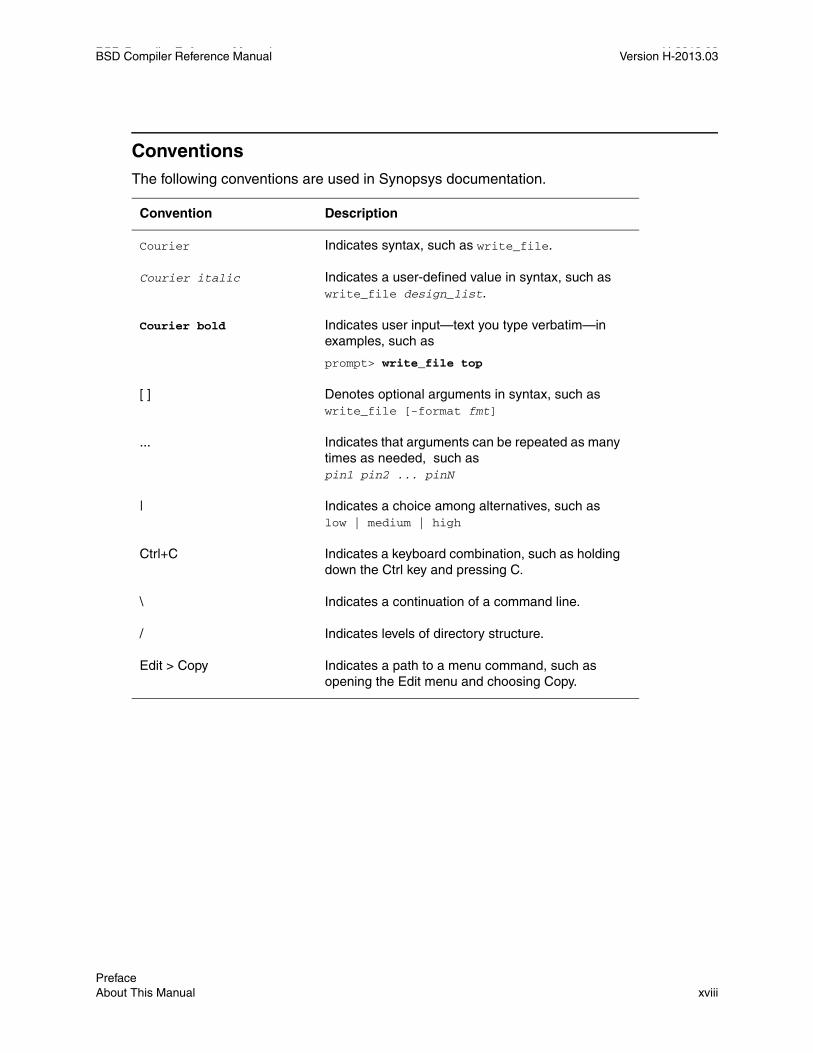
ConventionsThe following conventions are used in Synopsys documentation.
Convention Description
Courier Indicates syntax, such as write_file.
Courier italic Indicates a user-defined value in syntax, such as write_file design_list.
Courier bold Indicates user input—text you type verbatim—in examples, such as
prompt> write_file top
[ ] Denotes optional arguments in syntax, such as write_file [-format fmt]
... Indicates that arguments can be repeated as many times as needed, such as pin1 pin2 ... pinN
| Indicates a choice among alternatives, such as low | medium | high
Ctrl+C Indicates a keyboard combination, such as holding down the Ctrl key and pressing C.
\ Indicates a continuation of a command line.
/ Indicates levels of directory structure.
Edit > Copy Indicates a path to a menu command, such as opening the Edit menu and choosing Copy.
Preface About This Manual xviii

BSD Compiler Reference Manual Version H-2013.03
Customer Support
Customer support is available through SolvNet online customer support and through contacting the Synopsys Technical Support Center.
Accessing SolvNetSolvNet includes an electronic knowledge base of technical articles and answers to frequently asked questions about Synopsys tools. SolvNet also gives you access to a wide range of Synopsys online services including software downloads, documentation on the Web, and “Enter a Call to the Support Center.”
To access SolvNet, go to the SolvNet Web page at the following address:
https://solvnet.synopsys.com
If prompted, enter your user name and password. If you do not have a Synopsys user name and password, follow the instructions to register with SolvNet.
If you need help using SolvNet, click HELP in the top-right menu bar or in the footer.
Contacting the Synopsys Technical Support CenterIf you have problems, questions, or suggestions, you can contact the Synopsys Technical Support Center in the following ways:
• Open a call to your local support center from the Web by going to https://solvnet.synopsys.com, entering your user name and password and then clicking “Enter a Call to the Support Center.”
• Send an e-mail message to your local support center.
❍ E-mail [email protected] from within North America.
❍ Find other local support center e-mail addresses at http://www.synopsys.com/Support/GlobalSupportCenters/Pages
• Telephone your local support center.
❍ Call (800) 245-8005 from within the continental United States.
❍ Call (650) 584-4200 from Canada.
❍ Find other local support center telephone numbers at http://www.synopsys.com/Support/GlobalSupportCenters/Pages
Chapter 1: Preface Customer Support 1-xixPreface Customer Support xix

BSD Compiler Reference Manual H-2013.03BSD Compiler Reference Manual Version H-2013.03
Preface Customer Support xx
1Boundary-Scan Concepts for IEEE Std 1149.1 1
This chapter describes background concepts and terminology for boundary scan, as well as specific elements of IEEE Std 1149.1.
This chapter includes the following sections:
• Boundary-Scan Principles
• IEEE Std 1149.1 Device Architecture
• Boundary-Scan Design Flow
1-1

BSD Compiler Reference Manual H-2013.03BSD Compiler Reference Manual Version H-2013.03
Boundary-Scan Principles
The fundamental component of the boundary-scan architecture is the boundary-scan cell. It can shift data through the device core logic or around the core logic, depending upon the test mode selected. These principles are discussed in the sections that follow.
History of Boundary Scan MethodologyIn the mid-1980s, a group of European test engineers, calling themselves the Joint European Test Action Group (JETAG), began to develop a methodology for including board-level test functionality into chip-level devices. When North American engineers joined the group, the group name became the Joint Test Action Group (JTAG). This group decided on a serial shift register that wrapped around the boundary of the device (Figure 1-1), which they called Boundary Scan. This group is responsible for the international standard for boundary scan, the IEEE Std 1149.1.
Figure 1-1 Serial-Shift Register Around Boundary of Device
The Boundary-Scan CellEach primary input signal and primary output signal emanating from the core logic is supplemented at the top level with a multipurpose memory element called a “boundary-scan cell” (See Figure 1-2). Cells on device primary inputs are called input cells; cells on primary outputs are called output cells.
Device
Serial Shift Register
Core Logic
Chapter 1: Boundary-Scan Concepts for IEEE Std 1149.1 Boundary-Scan Principles 1-2
BSD Compiler Reference Manual Version H-2013.03
Figure 1-2 Boundary-Scan Cell
These boundary-scan cells can capture data into the device core logic in parallel mode (PI to PO), or shift it around the device core logic in serial mode (SI to SO), depending upon the mode of testing you choose. Figure 1-3 illustrates the serial and parallel nature of boundary-scan cells.
Figure 1-3 Serial Shift and Parallel Capture in Boundary Scan
Boundary Scan in Parallel ModeIn the parallel operation mode, the collection of boundary-scan cells is configured into a parallel-in, parallel-out shift register. A parallel load operation is called a “capture” operation. During the capture operation, signal values on device input pins are loaded into input cells, and signal values passing from the core logic to device output pins are loaded into output cells (see Figure 1-4).
PI
PO
SI SOMemoryElement
(Parallel In)
(Parallel Out)
(Serial In) (Serial Out)
Core LogicPI
PO
SI SOMemoryElement
Chapter 1: Boundary-Scan Concepts for IEEE Std 1149.1 Boundary-Scan Principles 1-3Chapter 1: Boundary-Scan Concepts for IEEE Std 1149.1 Boundary-Scan Principles 1-3
BSD Compiler Reference Manual H-2013.03BSD Compiler Reference Manual Version H-2013.03
Figure 1-4 Parallel Capture Operation
A parallel unload operation is called an “update” operation. During the update operation, signal values present in the input cells are passed from the device input pins into the core logic, replacing values on the device input pins, and signal values already present in the output scan cells are passed out through the device output pins, replacing output values generated by the core logic (see Figure 1-5).
Figure 1-5 Parallel Update Operation
Boundary Scan in Serial ModeData can also be shifted around the shift register in serial mode, starting from a dedicated test data in (TDI) device input pin and terminating at a dedicated device output pin, called test data out (TDO). The test clock (TCK) is fed in through yet another dedicated device input pin and the mode operation is controlled by a dedicated test mode select (TMS) serial control signal (see Figure 1-6).
Signal value is captured into the input cell
Signal value is loaded into the output cell
core logic
PI
PO
PI
PO
core logic
Signal value is passed into the core logic
Signal value is passed out of output cell
PI
PO
PI
PO
Chapter 1: Boundary-Scan Concepts for IEEE Std 1149.1 Boundary-Scan Principles 1-4
BSD Compiler Reference Manual Version H-2013.03
Figure 1-6 Boundary-Scan Serial Mode
Boundary-Scan Architecture SummaryThe concepts of boundary scan operating in parallel mode and in serial mode are summarized in Figure 1-7.
Figure 1-7 Boundary-Scan Concepts Summarized
Using the Boundary-Scan PathAt the device level, the boundary-scan elements contribute nothing to the functionality of the core logic. In fact, the boundary-scan path is independent of the function of the device. The value of the scan path is at the board level, because it allows you to test many devices at the same time.
Test Data In (TDI)Test Clock (TCK)
Test Mode Select (TMS)Test Data Out (TDO)
SI
SO
Core Logic
PI
PO
SI SOMemoryElement
Test Data In (TDI)
Test Clock (TCK)
Test Mode Select (TMS)
Test Data Out (TDO)
Chapter 1: Boundary-Scan Concepts for IEEE Std 1149.1 Boundary-Scan Principles 1-5Chapter 1: Boundary-Scan Concepts for IEEE Std 1149.1 Boundary-Scan Principles 1-5
BSD Compiler Reference Manual H-2013.03BSD Compiler Reference Manual Version H-2013.03
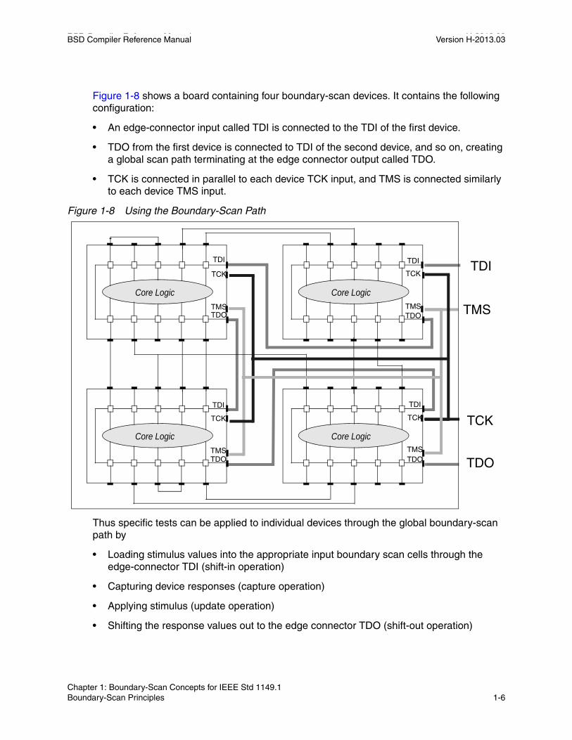
Figure 1-8 shows a board containing four boundary-scan devices. It contains the following configuration:
• An edge-connector input called TDI is connected to the TDI of the first device.
• TDO from the first device is connected to TDI of the second device, and so on, creating a global scan path terminating at the edge connector output called TDO.
• TCK is connected in parallel to each device TCK input, and TMS is connected similarly to each device TMS input.
Figure 1-8 Using the Boundary-Scan Path
Thus specific tests can be applied to individual devices through the global boundary-scan path by
• Loading stimulus values into the appropriate input boundary scan cells through the edge-connector TDI (shift-in operation)
• Capturing device responses (capture operation)
• Applying stimulus (update operation)
• Shifting the response values out to the edge connector TDO (shift-out operation)
Core Logic
Core Logic
Core Logic
Core Logic
TDI
TDI
TDI
TCK
TCK
TCK
TCK
TMS
TMS
TMS
TMS
TDO
TDO
TDO
TDO
TDITDI
TCK
TMS
TDO
Chapter 1: Boundary-Scan Concepts for IEEE Std 1149.1 Boundary-Scan Principles 1-6

BSD Compiler Reference Manual Version H-2013.03
Purpose of Boundary-Scan TestingBoundary scan’s primary purpose is to test for manufacturing defects such as
• Missing devices
• Damaged devices
• Open and short circuits
• Misaligned devices
• Wrong devices
These manufacturing defects can be caused by
• Electrical shock (electrostatic discharge)
• Mechanical shock (poor handling)
• Thermal shock (solder hot spots)
If such defects occur, they are likely to be present in the periphery of the device, in the solder, or in the interconnect between devices. Damage to the core logic of the device is rarely seen without damage to the periphery as well.
Thus the boundary-scan logic is well placed—at the boundary of the core logic of the device and at the boundary of the interconnect paths between devices.
Boundary-scan testing can be used to test the core logic functionality of a device or the interconnect structure between devices. Testing the core logic functionality of a device is called internal testing (Intest), and testing the interconnect structure is called external testing (Extest).
External testing provides a method to search for opens and shorts, and to test for manufacturing defects around the periphery of the device. Internal testing provides a method for testing the minimum functionality of the core logic of the device, such as existence testing.
Board Test StrategyA general-purpose strategy for testing a boundary-scan board can be performed in three steps:
1. Perform a boundary-scan infrastructure test.
This step tests the IEEE Std 1149.1 logic.
Chapter 1: Boundary-Scan Concepts for IEEE Std 1149.1 Boundary-Scan Principles 1-7Chapter 1: Boundary-Scan Concepts for IEEE Std 1149.1 Boundary-Scan Principles 1-7

BSD Compiler Reference Manual H-2013.03BSD Compiler Reference Manual Version H-2013.03
2. Apply stimulus and capture responses across the interconnect structures between the devices on the board. (This is the major application of boundary scan.)
This step tests the regions most susceptible to assembly damage caused by electrical, mechanical, or thermal shock.
3. Either carry out a limited existence test on the individual devices or initiate device self-test routines.
This step tests that the right devices are in their correct positions on the board. Device self-test can be as limited as an existence test, or it can perform its own testing to greater than 98% fault coverage.
IEEE Std 1149.1 Device Architecture
The IEEE Std 1149.1 architecture contains the following elements:
• An n-bit (n > = 2) instruction register (IR), holding the current instruction
• Four required and one optional test pins, collectively referred to as the test access port (TAP) (These pins are shown in Table 1-1.)
• A finite state machine TAP controller with inputs TCK and TMS
• A 1-bit bypass register
• An optional 32-bit identification register capable of being loaded with a permanent device identification code
• A boundary-scan cell on each device primary input and primary output pin, connected internally to form a serial scan path (collectively called the boundary-scan register)
Table 1-1 Test Access Port Pins
Test pin name Description
TDI Test Data In
TMS Test Mode Select
TCK Test Clock
TDO Test Data Out
TRST* Test Reset (IEEE Std 1149.1 Optional)
Chapter 1: Boundary-Scan Concepts for IEEE Std 1149.1 IEEE Std 1149.1 Device Architecture 1-8
BSD Compiler Reference Manual Version H-2013.03
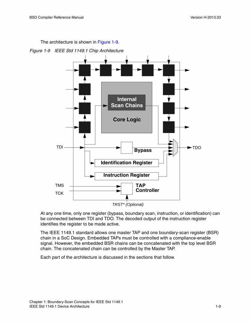
The architecture is shown in Figure 1-9.
Figure 1-9 IEEE Std 1149.1 Chip Architecture
At any one time, only one register (bypass, boundary scan, instruction, or identification) can be connected between TDI and TDO. The decoded output of the instruction register identifies the register to be made active.
The IEEE 1149.1 standard allows one master TAP and one boundary-scan register (BSR) chain in a SoC Design. Embedded TAPs must be controlled with a compliance-enable signal. However, the embedded BSR chains can be concatenated with the top level BSR chain. The concatenated chain can be controlled by the Master TAP.
Each part of the architecture is discussed in the sections that follow.
TDOTDIBypass
Identification Register
Instruction Register
TAPController
TRST* (Optional)
Internal
Core Logic
Scan Chains
TCK
TMS
Chapter 1: Boundary-Scan Concepts for IEEE Std 1149.1 IEEE Std 1149.1 Device Architecture 1-9Chapter 1: Boundary-Scan Concepts for IEEE Std 1149.1 IEEE Std 1149.1 Device Architecture 1-9

BSD Compiler Reference Manual H-2013.03BSD Compiler Reference Manual Version H-2013.03
Instruction RegisterThe instruction register has a shift section that can be connected to TDI and TDO, and a hold section, which holds the current instruction. There might be some decoding logic between the two sections, depending on the width of the register and the number of different instructions.
The TAP controller originates the control signals sent to the instruction register. The signals can either cause a shift-in, shift-out through the instruction register shift section, or cause the contents of the shift section to be passed across to the hold section in an update operation. It is also possible to load certain hard-wired values into the shift section of the instruction register in a capture operation.
The instruction register must be at least 2 bits long to allow coding of the three mandatory instructions, but the maximum length of the instruction register is not defined. The DW_tap_uc component from the foundation library specifies the maximum length of the IR to be 32 bits.
In capture mode, the two least significant bits (those bits closest to the TDO) must capture a 01 pattern, as shown in Figure 1-10. The values captured into higher-order bits are not defined by the standard. The higher-order bits can be used as an informal identification code register, for example. If the 32-bit identification register is not implemented, the instruction register can capture an informal identification code.
Chapter 1: Boundary-Scan Concepts for IEEE Std 1149.1 IEEE Std 1149.1 Device Architecture 1-10

BSD Compiler Reference Manual Version H-2013.03
Figure 1-10 Instruction Register
Figure 1-11 shows an implementation of a typical instruction register cell.
TDOTDIBypass
Identification Register
Instruction Register
TAPController
Internal
ClockDR
ShiftDR
UpdateDR
ClockIR
ShiftIR
UpdateIR
Enable
Select
Reset*
TMS
TCK
FromTDI
ToTDO
Hold Elements
Test Access
Port
Controller
}
Decoded output toselected data register
0 1Instruction Register length ≥ 2
TCKTMS
TRST*
Instruction Register
Shift Register
Decoder
}
Scan Chains
Core Logic
Chapter 1: Boundary-Scan Concepts for IEEE Std 1149.1 IEEE Std 1149.1 Device Architecture 1-11Chapter 1: Boundary-Scan Concepts for IEEE Std 1149.1 IEEE Std 1149.1 Device Architecture 1-11

BSD Compiler Reference Manual H-2013.03BSD Compiler Reference Manual Version H-2013.03
Figure 1-11 Typical Instruction Register Cell Design
InstructionsThe IEEE Std 1149.1 describes four mandatory instructions:
• EXTEST
The EXTEST instruction selects the boundary-scan register and performs operations on both the input boundary-scan register cells and on the output boundary-scan register cells. During EXTEST, all output boundary-scan register cells apply the value they hold to the output ports. This is the update operation in EXTEST. During the same EXTEST instruction, all input boundary-scan register cells can sample the values coming into the device. This is the capture operation in EXTEST. Thus, the EXTEST instruction allows for the testing of interconnections at the board level between different devices.
• BYPASS
The bypass instruction causes the device under test to be bypassed. The BYPASS instruction is assigned the all-1s code. When it is executed, it causes the bypass register to be placed between the TDI and TDO pins.
By definition, the initialized state of the hold section of the instruction register contains the BYPASS instruction, unless the informal identification register is implemented, in which case the IDCODE instruction is present in the hold section.
• SAMPLE
The SAMPLE instruction selects the boundary-scan register. During SAMPLE instruction, the operations of the test logic have no effect on the operations of the on-chip system logic or on the flow of signals between the system pins and the on-chip system logic. During SAMPLE instruction, the states of all the signals flowing from the on-chip system logic or through the system pins (input or output) are captured in the
ShiftIR
Data
From last cell
ClockIRTo Next Cell
G
1
11D
C1
TRST*
Reset &
UpdateIR
1D
C1
R
Instruction bit
Chapter 1: Boundary-Scan Concepts for IEEE Std 1149.1 IEEE Std 1149.1 Device Architecture 1-12
BSD Compiler Reference Manual Version H-2013.03
boundary-scan register cell (on the rising edge of TCK in the Capture-Dr controller state).
• PRELOAD
The PRELOAD instruction selects the boundary-scan register. During PRELOAD instruction, the operations of the test logic have no effect on the operations of the on-chip system logic or on the flow of signals between the system pins and the on-chip system logic. During PRELOAD instruction, parallel output registers/latches included in the boundary-scan register cells, load the data held in the associated shift-register stage (on the falling edge of TCK in the Update-Dr controller state).
Optionally, you can merge the SAMPLE and PRELOAD instructions by using the same opcodes.
See “Binary Code Assignments” on page 2-49 for codes for implementing the aforementioned mandatory instructions.
The IEEE Std 1149.1 defines a number of optional instructions. Optional instructions include
• INTEST
The INTEST instruction selects the boundary-scan register before applying test to the core logic of the device.
• IDCODE
The IDCODE instruction makes the identification register between TDI and TDO active, before loading the identification code and reading it out through TDO.
Note: If there is no device identification register (IDCODE) in the design, the BYPASS instruction is loaded into the instruction register during test logic reset.
• USERCODE
The USERCODE instruction selects the device identification register (DIR), which allows you to program the IDCODE. You must specify the IDCODE prior to this instruction.
• RUNBIST
The RUNBIST instruction initiates an internal self-test routine and places the pass/fail result register between TDI and TDO.
Two instructions introduced in the revised IEEE Std 1149.1a are
• CLAMP
The CLAMP instruction is established initially with the SAMPLE and PRELOAD instructions. It drives preset values onto the outputs of devices and then, unlike the SAMPLE and PRELOAD instructions, it selects the bypass register between TDI and
Chapter 1: Boundary-Scan Concepts for IEEE Std 1149.1 IEEE Std 1149.1 Device Architecture 1-13Chapter 1: Boundary-Scan Concepts for IEEE Std 1149.1 IEEE Std 1149.1 Device Architecture 1-13

BSD Compiler Reference Manual H-2013.03BSD Compiler Reference Manual Version H-2013.03
TDO. CLAMP can be used to set values on the outputs of certain devices to avoid bus contention problems, for example.
• HIGHZ
The HIGHZ instruction is similar to CLAMP, but it leaves the device output pins in their high impedance state. HIGHZ also selects the bypass register between TDI and TDO.
All instruction opcodes except BYPASS are undefined. Because four instructions are mandatory, the minimum length of the instruction register is 2 bits. The maximum length when using BSD Compiler is 32 bits. Any particular instruction can have more than one code and unused codes are mandated by IEEE Std 1149.1 to be interpreted as BYPASS.
Note: The designer can use certain codes to implement private instructions, that is, instructions whose functions are not made public. In these circumstances, the designer must define these codes to be private so that the user can avoid loading the codes. All unused codes must decode to BYPASS.
Using the Instruction RegisterThis section discusses how to load the instruction register and how to decode its contents. Figure 1-12 shows three devices on a circuit board, each connected in parallel to the board level TMS and TCK circuits. Chip 1 is connected to the board’s TDI. Each subsequent chip’s TDI is connected to the previous chip’s TDO.
Figure 1-12 Using the Instruction Register
In Figure 1-12, Chip 1 is placed in bypass mode, and Chip 2 and Chip 3 are placed in extest mode. Chip 1 is placed in bypass mode so that the time to get test stimulus to subsequent devices is reduced. Chip 2 and Chip 3 are placed in extest mode so that those devices can be readied for tests to check the interconnect between them.
TMS
TCK
Chip1 Chip2 Chip3
BoardTDO
BoardTDI
TDOTDI
Bypass
Identification Register
Instruction Register
TAPController
Internal
TDOTDI
Bypass
Identification Register
Instruction Register
TAPController
Internal
TDOTDI
Bypass
Identification Register
Instruction Register
TAPController
Internal
Chapter 1: Boundary-Scan Concepts for IEEE Std 1149.1 IEEE Std 1149.1 Device Architecture 1-14

BSD Compiler Reference Manual Version H-2013.03
To set these modes, it is necessary to load the bypass instruction (all-1s) into the instruction register of Chip 1, and the extest instruction (all-0s) into the instruction registers of Chip 2 and Chip 3.
This is accomplished in three steps:
1. Connect the instruction registers of all three devices between their respective TDI and TDO pins. This is done from the TAP controller by way of the TMS line, which is connected in parallel to each device.
2. Load the appropriate instructions into each chip’s instruction register. If each instruction register is 2 bits long, this operation is a serial load of 110000 into the board TDI, which places 00 on each of the instruction registers of Chips 2 and 3, and 11 on the instruction register of Chip 1. The instruction registers are now set up with the correct instructions loaded in their shift sections.
3. Continue with the values on TMS to cause each TAP controller to issue the control signal values to cause the value in the shift sections of the instruction registers to be transferred to the hold sections where they become the current instruction. This is the Update operation.
At this point the instructions are carried out:
1. Chip 1 deselects the instruction register and selects the bypass register between TDI and TDO.
2. Chips 2 and 3 deselect their instruction registers and select their boundary-scan registers between TDI and TDO.
3. Chips 2 and 3 are now ready for the extest operation.
The resulting states of the three devices are shown in Figure 1-13.
Chapter 1: Boundary-Scan Concepts for IEEE Std 1149.1 IEEE Std 1149.1 Device Architecture 1-15Chapter 1: Boundary-Scan Concepts for IEEE Std 1149.1 IEEE Std 1149.1 Device Architecture 1-15

BSD Compiler Reference Manual H-2013.03BSD Compiler Reference Manual Version H-2013.03
Figure 1-13 Board After Instruction Register Sequence
Test Access PortThe test access port (TAP) consists of four mandatory terminals plus one optional terminal. Its elements are shown in Figure 1-14.
TMS
TCK
Chip1 Chip2 Chip3
BoardTDO
BoardTDI
TDOTDI
Bypass
Identification Register
Instruction Register
TAPController
Internal
TDOTDI
Bypass
Identification Register
Instruction Register
TAPController
Internal
TDOTDI
Bypass
Identification Register
Instruction Register
TAPController
Internal
Chapter 1: Boundary-Scan Concepts for IEEE Std 1149.1 IEEE Std 1149.1 Device Architecture 1-16

BSD Compiler Reference Manual Version H-2013.03
Figure 1-14 Test Access Port
The five terminals are
• Test data in (TDI)
Serial test data in with a default of 1 (pullup).
• Test data out (TDO)
Serial test data out with a default of Z. Only active during a shift operation.
• Test mode select (TMS)
Serial input control signal with a default of 1 (pullup).
• Test clock (TCK)
Dedicated test clock, any convenient frequency.
• Test reset (TRST*) (IEEE Std. 1149.1 optional)
Asynchronous TAP controller reset with default of 1 (pullup) and active low.
Several additional terminals are included in the TAP controller. They are listed in Table 2-3 on page 2-27. For more information about each of these terminals, refer to the BSD Compiler User Guide or the IEEE Std. 1149.1 Specification.
TDOTDIBypass
Identification Register
Instruction Register
TAPController
Internal
TCKTMS
Instruction Register
Scan Chains
Core Logic
Chapter 1: Boundary-Scan Concepts for IEEE Std 1149.1 IEEE Std 1149.1 Device Architecture 1-17Chapter 1: Boundary-Scan Concepts for IEEE Std 1149.1 IEEE Std 1149.1 Device Architecture 1-17

BSD Compiler Reference Manual H-2013.03BSD Compiler Reference Manual Version H-2013.03
Control SignalsThe TMS, TCK, and TRST* terminals go to a finite state machine controller that produces control signals. These signals include dedicated signals to the instruction register and generic signals to all data registers. The finite state machine is shown in Figure 1-16 on page 1-19.
The following are dedicated signals to the instruction register:
• ClockIR
• ShiftIR
• UpdateIR
The following are generic signals to all data registers:
• ClockDR
• ShiftDR
• UpdateDR
The following are additional generic signals:
• Select
• Reset
• Enable
The TAP controller is illustrated in Figure 1-15.
Figure 1-15 TAP Controller
ClockDRShiftDRUpdateDRResetSelectClockIRShiftIRUpdateIRenable
TMS
TCK
TRST*(IEEE Std. 1149.1 optional)
TestAccess
PortController
Chapter 1: Boundary-Scan Concepts for IEEE Std 1149.1 IEEE Std 1149.1 Device Architecture 1-18

BSD Compiler Reference Manual Version H-2013.03
Finite State Machine TAP ControllerThe TAP controller contains 16 states. The state diagram is shown in Figure 1-16.
Figure 1-16 State Table for the TAP Controller
The state table is described as follows:
• A state transition occurs on the positive edge of TCK, and output values change on the negative edge of TCK. The value on the state transition arcs is the value of TMS.
• The TAP controller is initialized in the “Test_Logic Reset” state, the “Asleep” state. While TMS remains at its default of 1, the state remains unchanged. (See Figure 1-17.)
Select_DR-Scan
Capture_DR
Shift_DR
Exit1_DR
Pause_DR
Exit2_DR
Update_DR
Select_IR-Scan
Capture_IR
Shift_IR
Exit1_IR
Pause_IR
Exit2_IR
Update_IR
Test-Logic-Reset
Run-Test/Idle
1
0
01 1 1
0 0
0 0
0 0
1 1
1 1
1 1
1 01 0
1 1
0 0
0
0
0
0
1 1
Data Column Instruction Column
Chapter 1: Boundary-Scan Concepts for IEEE Std 1149.1 IEEE Std 1149.1 Device Architecture 1-19Chapter 1: Boundary-Scan Concepts for IEEE Std 1149.1 IEEE Std 1149.1 Device Architecture 1-19

BSD Compiler Reference Manual H-2013.03BSD Compiler Reference Manual Version H-2013.03
Figure 1-17 TAP Initialization State
• Pulling TMS low causes a transition to the Run_Test Idle state, the “Awake and Do Nothing” state. (See Figure 1-18.)
Figure 1-18 TAP TMS Transition From Initialization State
• Typically, the next state selected is the Select_IR_Scan state so that the TAP can be ready to load and execute a new instruction. An additional “11” sequence on TMS achieves this. (See Figure 1-19.)
Figure 1-19 TAP Ready to Load and Execute State
• From here the TAP controller can move through the various Capture_IR, Shift_IR, Update_IR states as required. (See Figure 1-20.)
Test-Logic-Reset1
0
Test-Logic-Reset
Run-Test/Idle
1
0
0
Select_DR-Scan Select_IR-Scan
Test-Logic-Reset
Run-Test/Idle
1
0
01 1
Chapter 1: Boundary-Scan Concepts for IEEE Std 1149.1 IEEE Std 1149.1 Device Architecture 1-20

BSD Compiler Reference Manual Version H-2013.03
Figure 1-20 TAP State Table for the Instruction Column
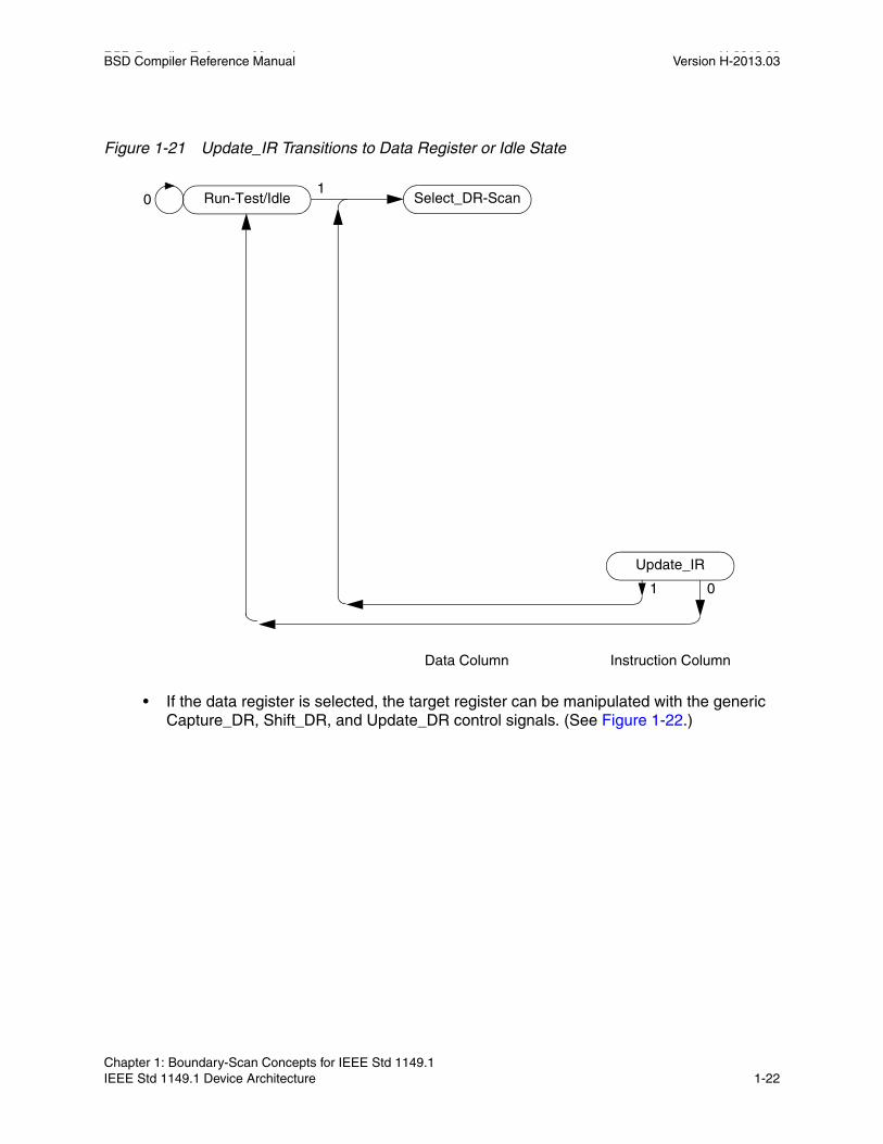
• The last operation in the instruction column is the Update_IR operation. Here the instruction loaded into the shift section of the instruction register is transferred to the hold section to become the current instruction.
• The instruction register is then deselected as the register connected between TDI and TDO. The data register is selected if the value shifted out of TMS = 1. The Run_Test/Idle state is selected if the TMS = 0. (See Figure 1-21.)
Select_IR-Scan
Capture_IR
Shift_IR
Exit1_IR
Pause_IR
Exit2_IR
Update_IR
0
0
0
1
1
1
1
0
0
0
1
Instruction Column
1
Chapter 1: Boundary-Scan Concepts for IEEE Std 1149.1 IEEE Std 1149.1 Device Architecture 1-21Chapter 1: Boundary-Scan Concepts for IEEE Std 1149.1 IEEE Std 1149.1 Device Architecture 1-21
BSD Compiler Reference Manual H-2013.03BSD Compiler Reference Manual Version H-2013.03
Figure 1-21 Update_IR Transitions to Data Register or Idle State
• If the data register is selected, the target register can be manipulated with the generic Capture_DR, Shift_DR, and Update_DR control signals. (See Figure 1-22.)
Select_DR-Scan
Update_IR
Run-Test/Idle01
1 0
Data Column Instruction Column
Chapter 1: Boundary-Scan Concepts for IEEE Std 1149.1 IEEE Std 1149.1 Device Architecture 1-22
BSD Compiler Reference Manual Version H-2013.03
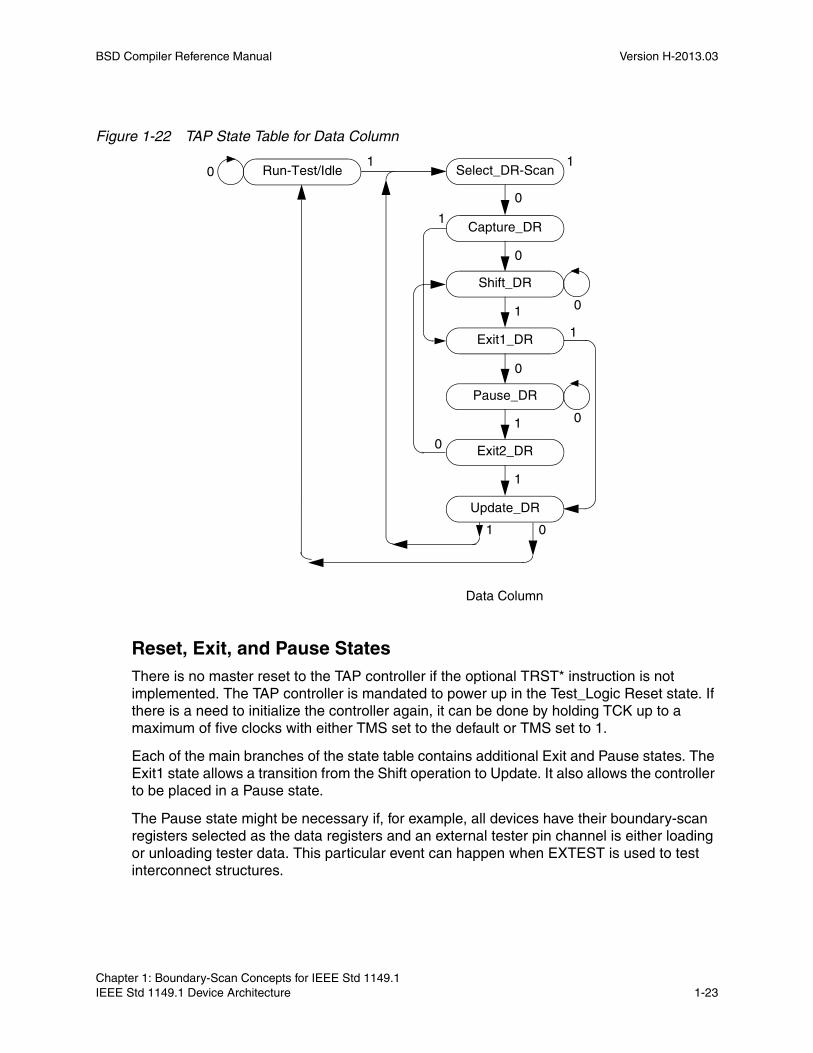
Figure 1-22 TAP State Table for Data Column
Reset, Exit, and Pause StatesThere is no master reset to the TAP controller if the optional TRST* instruction is not implemented. The TAP controller is mandated to power up in the Test_Logic Reset state. If there is a need to initialize the controller again, it can be done by holding TCK up to a maximum of five clocks with either TMS set to the default or TMS set to 1.
Each of the main branches of the state table contains additional Exit and Pause states. The Exit1 state allows a transition from the Shift operation to Update. It also allows the controller to be placed in a Pause state.
The Pause state might be necessary if, for example, all devices have their boundary-scan registers selected as the data registers and an external tester pin channel is either loading or unloading tester data. This particular event can happen when EXTEST is used to test interconnect structures.
Select_DR-Scan
Capture_DR
Shift_DR
Exit1_DR
Pause_DR
Exit2_DR
Update_DR
Run-Test/Idle01 1
0
0
0
1
1
1
1 0
1
0
0
0
1
Data Column
Chapter 1: Boundary-Scan Concepts for IEEE Std 1149.1 IEEE Std 1149.1 Device Architecture 1-23Chapter 1: Boundary-Scan Concepts for IEEE Std 1149.1 IEEE Std 1149.1 Device Architecture 1-23

BSD Compiler Reference Manual H-2013.03BSD Compiler Reference Manual Version H-2013.03
In another situation, the length of the chained boundary-scan registers might be longer than the memory associated with the tester channel. In this case, it is necessary to update or unload the content of the channel memory before resuming the shift operation through the boundary-scan path. The Pause state enables this action, and the Exit2 state allows a return to the shift operation.
TAP Controller Logic RequirementsIn general, a TAP controller requires four state flip-flops and another four flip-flops to hold the values of certain output signals.
Bypass RegisterThe bypass register is a 1-bit register that is selected by the BYPASS instruction. It is shown in Figure 1-23.
Figure 1-23 Bypass Register
The bypass register provides a basic shift function. There is no parallel output, which means that the Update_DR control has no effect on the register, but there is a defined effect with the Capture_DR control—the register captures a hard-wired value of 0.
A typical bypass register design is shown in Figure 1-24.
TDOTDIBypass
Identification Register
Instruction Register
TAPController
Internal
TCKTMS
Instruction Register
Scan Chains
Core Logic
Chapter 1: Boundary-Scan Concepts for IEEE Std 1149.1 IEEE Std 1149.1 Device Architecture 1-24

BSD Compiler Reference Manual Version H-2013.03
Figure 1-24 Typical Bypass Register Design
Device Identification RegisterThe device identification register (DIR), which is optional, is a 32-bit register with capture and shift modes of operation. It is shown in Figure 1-25.
Figure 1-25 Device Identification Register
Shift_DR
From TDI
To TDO1D
C1
&
Clock_DR
TDOTDIBypass
Identification Register
Instruction Register
TAPController
Internal
TCKTMS
Instruction Register
Scan Chains
Core Logic
Chapter 1: Boundary-Scan Concepts for IEEE Std 1149.1 IEEE Std 1149.1 Device Architecture 1-25Chapter 1: Boundary-Scan Concepts for IEEE Std 1149.1 IEEE Std 1149.1 Device Architecture 1-25

BSD Compiler Reference Manual H-2013.03BSD Compiler Reference Manual Version H-2013.03
Note: Capture value for the USERCODE uses the same DIR.
The captured 32 bits identify the device through the following fields:
• Bit 0 (least significant bit—LSB) is always 1.
• Bits 1-11 identify the manufacturer of the device by using a compact form of the JEDEC identification code.
• Bits 12-27 provide a 16-bit free-format part number field.
• Bits 28-31 provide a 4-bit free format field to specify up to 16 different versions of the same basic device.
After it is captured, the 32-bit identification code can be shifted out through TDO for inspection. Figure 1-26 shows a possible implementation of the 32-bit register.
Figure 1-26 Device Identification Register Bits
On power-up, either the least significant bit of the identification register or the contents of the bypass register must be loaded into the hold stage of the device’s boundary-scan register. This requirement is mandated by IEEE Std 1149.1.
Boundary-Scan RegisterBoundary-scan cells are placed on device signal input, output, bidirectional, and tristate ports. These boundary-scan cells are linked together to form the boundary-scan register. The order of linking is determined by the physical adjacency of the pins or by layout constraints. The boundary-scan register is shown in Figure 1-27.
MSB
31 28 27
Ver Part Number Manufacturer ID
12
(4 bits) (16 bits) (11 bits) (1 bit)
Bit Number
1
11 1 0
LSB
Chapter 1: Boundary-Scan Concepts for IEEE Std 1149.1 IEEE Std 1149.1 Device Architecture 1-26

BSD Compiler Reference Manual Version H-2013.03
Figure 1-27 Boundary-Scan Register
The boundary-scan register is selected by the EXTEST, SAMPLE, PRELOAD, and INTEST instructions.
Boundary-Scan CellsA number of BSR cells are defined by IEEE Std 1149.1b. They are detailed in the following sections.
The BC_4 Cell
A basic boundary-scan cell is shown in Figure 1-28. The basic cell contains the minimal functionality to support boundary scan. It contains capture and shift, but not update functionality. The mandatory instructions in IEEE Std 1149.1 do not require update on input scan cells. The basic cell can be used on devices that are sensitive to extra loading on the data_in signals, such as system clocks. This cell is identified as a BC_4 cell by IEEE Std 1149.1b. Whenever the BC_4 cell is mentioned in this document, it refers to the design shown in Figure 1-28.
TDOTDIBypass
Identification Register
Instruction Register
TAPController
Internal
TCKTMS
Instruction Register
Scan Chains
Core Logic
Chapter 1: Boundary-Scan Concepts for IEEE Std 1149.1 IEEE Std 1149.1 Device Architecture 1-27Chapter 1: Boundary-Scan Concepts for IEEE Std 1149.1 IEEE Std 1149.1 Device Architecture 1-27

BSD Compiler Reference Manual H-2013.03BSD Compiler Reference Manual Version H-2013.03
Figure 1-28 Basic Boundary-Scan Cell—BC_4
The benefit to using the BC_4 cell is that it is small. It has only one flip-flop and only one multiplexer (MUX). It is observable but it is not controllable. Because of this, the INTEST instruction cannot be supported on the BC_4 BSR cell.
The BC_1 Cell
A more generic boundary-scan cell is shown in Figure 1-29. This cell is full featured, containing capture, shift, and update functionality. The generic boundary-scan cell can be used for both input and output boundary-scan cells. The generic boundary-scan cell has separate flip-flops for the shift and hold functions. By using this generic boundary-scan cell, you can shift through the shift path without disturbing the hold data. This cell is identified as a BC_1 cell by IEEE Std 1149.1b. Whenever the BC_1 cell is mentioned in this document, it refers to the design shown in Figure 1-29. The mode signal generation for the BC_1 cell is shown in Table 1-2.
Table 1-2 Mode Signal Generation for BC_1
Instruction Mode for input cell Mode for output cell
EXTEST 1 1
SAMPLE 0 0
PRELOAD 0 0
INTEST 1 1a
RUNBIST 1 1
CLAMP 1 1
BYPASS 0 0
Shift_DR
Data_In
Scan_in
Clock_DR
Scan_Out
G
1
11D
C1
(from system pin)
(from last BS cell)(to next BS cell)
Data_Out(to system logic)
Q
CAP
Chapter 1: Boundary-Scan Concepts for IEEE Std 1149.1 IEEE Std 1149.1 Device Architecture 1-28

BSD Compiler Reference Manual Version H-2013.03
Figure 1-29 Basic Boundary-Scan Cell—BC_1
The BC_1 cell is useful because it is both controllable and observable. It supports the INTEST instruction when it is placed on input ports.
The BC_2 Cell
Another type of generic boundary-scan cell is shown in Figure 1-30. It is quite similar to the BC_1 cell. The difference in behavior between the two cells is the value captured in the capture flip-flop when the mode signal is active. In the BC_1 cell, the value captured is the value of the primary input (data_in). In the BC_2 cell, the value captured is the value of the update flip-flop. The mode signal generation for the BC_2 cell is shown in Table 1-3.
a. If you do not want these instructions to drive the output pins with preloaded data held in the boundary-scan register, then these instructions are not needed to determine the state of the mode signal. Instead, the HIGHZ instruction must be added to the output enable logic to force every system output pin to an inactive drive state.
Table 1-3 Mode Signal Generation for BC_2
Instruction Mode for Input Cell Mode for Output Cell
EXTEST 0 1
SAMPLE 0 0
PRELOAD 0 0
Shift_DR
Data_In
Scan_in Clock_DR
Scan_Out
G
1
11D
C1
Q
Data_Out
G
1
1
1D
C1
Q
Update_DR
Mode
(to next BS cell)
(from last BS cell)
CAP UPD
(from
(to system pin)system logic)
Chapter 1: Boundary-Scan Concepts for IEEE Std 1149.1 IEEE Std 1149.1 Device Architecture 1-29Chapter 1: Boundary-Scan Concepts for IEEE Std 1149.1 IEEE Std 1149.1 Device Architecture 1-29

BSD Compiler Reference Manual H-2013.03BSD Compiler Reference Manual Version H-2013.03
Figure 1-30 Basic Boundary-Scan Cell—BC_2
As a result of this difference, the BC_2 cell is more testable than the BC_1 cell.
Note: IEEE Std. 1149.1 does not support INTEST for BC_2 cells on output2. An output2 is a cell that drives a two-state output (either symmetric or asymmetric).
INTEST 1 Not supported
CLAMP X 1
RUNBIST X 1a
BYPASS 0 0
a. If you do not want these instructions to drive the output pins with preloaded data held in the boundary-scan register, these instructions are not needed to determine the state of the mode signal. Instead, the HIGHZ instruction must be added to the output enable logic to force every system output pin to an inactive drive state.
Table 1-3 Mode Signal Generation for BC_2 (Continued)
Instruction Mode for Input Cell Mode for Output Cell
Shift_DRData_In
Scan_in Clock_DR
Scan_Out
G
1
11D
C1
Q 1D
C1
Q
Update_DR
G
1
1
Data_out
Mode
from system logic
(from last BS cell)
(to next BS cell)
(to system pin)
CAP UDP
Chapter 1: Boundary-Scan Concepts for IEEE Std 1149.1 IEEE Std 1149.1 Device Architecture 1-30

BSD Compiler Reference Manual Version H-2013.03
The BC_7 Cell
One cell can combine the function of two generic cells for bidirectional ports. The combined boundary-scan cell is shown in Figure 1-31. Depending on the value of the mode1 signal, the cell is either a boundary-scan cell for the input side or a boundary-scan cell for the output side of the bidirectional port. The mode signal generation for the BC_7 cell is shown in Table 1-4.
Table 1-4 Mode Signal Generation for BC_7
Instruction Mode1 Mode 2 Mode 3
EXTEST 1 0 1
SAMPLE 0 0 1
PRELOAD 0 0 1
INTEST 0 1 0
CLAMP 1 X 1
RUNBIST X X 0
HIGHZ X X 0
Chapter 1: Boundary-Scan Concepts for IEEE Std 1149.1 IEEE Std 1149.1 Device Architecture 1-31Chapter 1: Boundary-Scan Concepts for IEEE Std 1149.1 IEEE Std 1149.1 Device Architecture 1-31

BSD Compiler Reference Manual H-2013.03BSD Compiler Reference Manual Version H-2013.03
Figure 1-31 Generic Boundary-Scan Cell—BC_7 for Bidirectional Pins
Note: The BC_7 cell can be configured in only one function at a time. It is well suited to bidirectionals that are tested at a given time as inputs or as outputs.
This cell is identified as a BC_7 cell by IEEE Std 1149.1b. Whenever the BC_7 cell is mentioned in this document, it refers to the design shown in Figure 1-31.
Adding Boundary-Scan Cells to Your DesignPrimarily, boundary-scan cells must be provided on all device input and output signal pins, with the exception of Power, Ground, and other analog signals. Note that there must be no logic between the pin and the boundary-scan cell with the exception of driver amplifiers or other forms of analog circuitry.
In the case of pin fanin, boundary-scan cells should be provided on each primary input to the core logic. In this way, each input can be set up with an independent value, thus providing the maximum flexibility for intest and assisting in checking for opens and shorts on input to the boundary-scan cell.
Similarly, for the case of pin fanout—if each output pin has a boundary-scan cell, EXTEST can set different and independent values.
&
&
G1
G1
G1
G1 G1
G1
1
1
1
1
1
1
1
1
1
1 1
1
1 1D 1D
1D 1D
C1 C1
C1C1
EN
Clock_DR Update_DRScan_in(from last BS cell)
Mode_2
Mode_1 Shift_DR Mode_3
Data_out(to system pin)
Scan_Out(to next BS cell)
OutputControl
OutputData
InputData
Chapter 1: Boundary-Scan Concepts for IEEE Std 1149.1 IEEE Std 1149.1 Device Architecture 1-32

BSD Compiler Reference Manual Version H-2013.03
Where there are tristate output pins, there must be a boundary-scan cell on the status control signal into the output driver buffer. A simple example of a tristate output pin is shown in Figure 1-32.
Figure 1-32 Control of Tristate Outputs
Up to three boundary-scan cells are required for bidirectional I/O pins—one on the input side, one on the output side, and one to allow the control of the I/O status. You can also use a BC_7 cell for the input/output data and combine it with a control cell to achieve the same result. A simple bidirectional pin is shown in Figure 1-33.
Figure 1-33 Control of Bidirectional I/O Pins
Accessing Other Core Logic RegistersIEEE Std 1149.1 allows for the definition and use of private instructions to access internal shift registers. For example, an optional instruction that accesses internal registers is RUNBIST.
Core Logic
TDI
TCK
TMS
TDO
Core Logic
TDI
TCK
TMS
TDO
Chapter 1: Boundary-Scan Concepts for IEEE Std 1149.1 IEEE Std 1149.1 Device Architecture 1-33Chapter 1: Boundary-Scan Concepts for IEEE Std 1149.1 IEEE Std 1149.1 Device Architecture 1-33

BSD Compiler Reference Manual H-2013.03BSD Compiler Reference Manual Version H-2013.03
RUNBIST is defined in IEEE Std 1149.1. Built-in self-test (BIST) must be self-initializing, and it must target a self-test result register between TDI and TDO. The TAP controller remains in its run-test/idle state for the duration of the test. The self-test clock can be TCK or some other suitable clock. When self-test is completed, the targeted register takes and holds the pass or fail result. This value cannot be changed by any subsequent pulses of TCK. This allows different length self-tests to be performed on different devices, so that when the self-test is complete across the entire board, all values can be clocked out.
Boundary-Scan Design Flow
Consider boundary-scan synthesis in the context of the entire IC-design process. It cannot be executed in isolation from the other tasks associated with developing a robust and appropriate boundary-scan interface for an integrated circuit.
Defining the boundary-scan architecture required for the integrated circuit requires understanding the types of testing tasks that are to be executed at the board or system level.
After boundary-scan logic insertion, the design must be checked for compliance with the IEEE Std 1149.1. Tolerable and intolerable violations of the standard must be analyzed and addressed, where necessary.
Manufacturing test vectors for the synthesized boundary-scan logic must be generated.
A description of the boundary-scan design (BSDL) must be generated for board test tools.
Figure 1-34 shows a design flow for creating boundary-scan logic on an integrated circuit.
Chapter 1: Boundary-Scan Concepts for IEEE Std 1149.1 Boundary-Scan Design Flow 1-34

BSD Compiler Reference Manual Version H-2013.03
Figure 1-34 Boundary-Scan Design Flow
Specifying Boundary-Scan RequirementsWhen you create a boundary-scan design, you must first prepare the interface between the core logic of your design and the top level. You must also define all the elements that are to be a part of the design. These steps include
• Ensuring each port of your top-level design has a corresponding pin
• Ensuring each TAP port has a corresponding pin
• Identifying boundary-scan instructions to be used
Chapter 1: Boundary-Scan Concepts for IEEE Std 1149.1 Boundary-Scan Design Flow 1-35Chapter 1: Boundary-Scan Concepts for IEEE Std 1149.1 Boundary-Scan Design Flow 1-35

BSD Compiler Reference Manual H-2013.03BSD Compiler Reference Manual Version H-2013.03
Inserting Boundary-Scan LogicDuring boundary-scan logic insertion, the tool synthesizes the design automatically. You control optimization within each command’s user interface.
Verifying IEEE Std 1149.1 ComplianceCheck the compliance of your design against the IEEE Std 1149.1. This aids in the testing of diverse designs on circuit boards. If your design is noncompliant, this step can assist you in examining the causes and eliminating problems.
Generating Boundary-Scan Description Language (BSDL)The characteristics of the boundary-scan architecture must be captured for downstream use by board- and system-level test generation tools.
If a Boundary-Scan Description Language (BSDL) file exists for the boundary-scan design, an automated test equipment (ATE) program generator can read it and map the circuit’s linkage to other circuits on the board, creating a board test.
Generating Functional and Leakage Test VectorsBecause boundary scan adds additional logic to your design, it is important to check its functionality on the tester. By generating a set of vectors that are dedicated to boundary-scan logic testing, you can verify this portion of the design. You can use these vectors for functional simulation or you can use them to get more accurate fault coverage on your completed design. The presence of boundary-scan logic close to the pads of your design enables you to characterize the pads using DC-parametric techniques. Leakage test vectors can be generated with the rest of the functional vectors to make DC-parametric testing possible. For more information on DC-parametric, see the BSD Compiler User Guide.
Chapter 1: Boundary-Scan Concepts for IEEE Std 1149.1 Boundary-Scan Design Flow 1-36

2Inserting Boundary-Scan Logic for IEEE Std 1149.1 2
This chapter describes how to insert boundary-scan logic into your design and preview the results before compliance checking. Various sections describe boundary-scan requirements, initializing and inserting the TAP controller, and implementing instructions.
This chapter includes the following sections:
• General Boundary-Scan Design Requirements
• TAP Controller Initialization
• Choosing an Asynchronous or Synchronous Boundary-Scan Implementation
• Choosing Boundary-Scan Components
• Design Requirements for Custom Boundary-Scan Components
• Inserting Boundary-Scan Logic
• The Effect of Boundary-Scan Register Cell Type Specifications
• Ordering Boundary-Scan Register Cells
• Inserting the TAP Controller
• Implementing Mandatory, Optional, and User-Defined Instructions
• Generating Mode Signals for the BSR Cells
2-1

BSD Compiler Reference Manual H-2013.03BSD Compiler Reference Manual Version H-2013.03
• Previewing Your Boundary-Scan Design
• Optimization Techniques
Chapter 2: Inserting Boundary-Scan Logic for IEEE Std 1149.1 2-2

BSD Compiler Reference Manual Version H-2013.03
General Boundary-Scan Design Requirements
After you load your top-level design description, you can insert boundary-scan logic into it.
While a minimum set of design elements must be present before you use the insert_dft command, there are also some design elements that, although not required, you might choose to incorporate.
Mandatory Design ElementsYou must perform the following activities on your design to run insert_dft successfully:
• Define the input, output, and bidirectional interface completely at the top level
• Connect a pad cell to each port
• Define the four mandatory TAP ports by using the set_dft_signal command
Nonmandatory Design ElementsYou are not required to perform the following activities on your design to run insert_dft successfully:
• Synthesize core logic before boundary-scan insertion
• Connect hierarchical logic to the other side of the pads used for the TAP ports
Pad CellsA library pad cell should contain special attributes that allow BSD Compiler to detect their presence. These attributes are
• pad_cell : true ;
This attribute is set on the library cell, and its value should be true.
• is_pad : true ;
This attribute is set on the library cell pin that is connected to the port, and its value should be true.
An example of a portion of the library cell, in which these attributes are defined, is shown in Example 2-1.
Chapter 2: Inserting Boundary-Scan Logic for IEEE Std 1149.1 General Boundary-Scan Design Requirements 2-3Chapter 2: Inserting Boundary-Scan Logic for IEEE Std 1149.1 General Boundary-Scan Design Requirements 2-3

BSD Compiler Reference Manual H-2013.03BSD Compiler Reference Manual Version H-2013.03
Example 2-1 Library Pad Cell
cell(IBUF1) { area : 2; pad_cell :
true; pin(A) { direction : input; capacitance : 1; is_pad :
true; hysteresis : true; input_voltage : CMOS_SCHMITT; ... }
You should make sure that each pad cell of your design has these two attributes set appropriately. If these attributes are missing on the pad cell, you can set them explicitly by using the set_attribute command as shown in Example 2-2.
Example 2-2 Setting Pad Cell Attributes
dc_shell> set_attribute find [lib_cell lsi_10k/IBUFF] \pad_cell true -type boolean
dc_shell> set_attribute find [lib_pin lsi_10k/IBUFF/A] \is_pad true -type boolean
Support for Differential I/O Pad CellsDifferential I/O library pad cells should contain special attributes that allow BSD Compiler to detect their presence. These attributes specify the following:
• When the noninverting pin equals 1 and the inverting pin equals 0, the signal gets logic 1.
• When the noninverting pin equals 0 and the inverting pin equals 1, the signal gets logic 0.
Use the complementary_pin attribute to identify the differential input inverting pin with which the noninverting pin is associated and from which it inherits timing information and associated attributes.
To set the complementary_pin attribute, use the following syntax in the library:
complementary_pin : "pin_name" ;
where the pin_name value identifies the differential input data inverting pin whose timing information and associated attributes the noninverting pin inherits. Only one input pin is modeled at the cell level. The associated differential inverting pin is defined in the same pin group as the noninverting pin. These settings are shown in Example 2-3.
Chapter 2: Inserting Boundary-Scan Logic for IEEE Std 1149.1 General Boundary-Scan Design Requirements 2-4

BSD Compiler Reference Manual Version H-2013.03
Example 2-3 Differential Library Pad Cell
cell (diff_buffer) {...pin (A) { /* noninverting pin /
direction : input ; complementary_pin :("AN") /* inverting_pin / }
}
Use the fault_model attribute to define the value when both complementary pins are driven to the same value. To set the fault_model attribute, use the syntax
fault_model : "two-value string" ;
For more information on the fault_model attribute, see the Library Compiler Liberty and Symbol Libraries Reference Manual.
Make sure that each differential pad cell of your design has these attributes set appropriately. If you define one of the ports of a differential pad as a linkage port, then set the complementary_pin attribute on the positive pin and the master_complement_pin attribute on the negative pin as shown in Example 2-4.
Example 2-4 Setting Differential Pad Cell Attributes
dc_shell> set_attribute find [lib_cell lib_name /cell_name ] \differential_cell true -type boolean
dc_shell> set_attribute find [lib_pin lib_name /cell_name \ pos_pin_name ] complementary_pin neg_pin_name -type string
dc_shell> set_attribute find [lib_pin lib_name /cell_name \ neg_pin_name ] master_complementary_pin pos_pin_name \
-type string
Support for Soft Macro Pad CellsThe define_dft_design command allows you to specify the location of the boundary-scan cell on the pad pin of a library cell, soft-macro cell, or wrapper for the library cell.
Soft macro pad cells have some basic requirements, which are described in the following paragraphs.
A structural gate-level (Verilog) model should be included in a single module or block and can contain multiple levels of hierarchy. The pins of the pad should belong to the same level of hierarchy.
The functionality described in the netlist will be characterized during preview_dft and insert_dft. The BSD specification is based on the structural gate-level (Verilog) model of your soft macro pad cells.
Chapter 2: Inserting Boundary-Scan Logic for IEEE Std 1149.1 General Boundary-Scan Design Requirements 2-5Chapter 2: Inserting Boundary-Scan Logic for IEEE Std 1149.1 General Boundary-Scan Design Requirements 2-5

BSD Compiler Reference Manual H-2013.03BSD Compiler Reference Manual Version H-2013.03
Before insertion, BSD Compiler checks that every port is connected to the pad library module or is identified as a pad. Connections from and to the BSR are made according to the signal types given to these pins; no modifications are allowed to the pad cell during insertion. The functional model for the soft macro pad is persistent and saved in the .ddc file representing the pad design.
Compliance checking is completed after insert_dft. You can characterize complex library pad cells to help BSD Compiler make the correct connections using the define_dft_design command. Doing this ensures both reference names and library cell names will be supported.
The new abstracted pad model is referenced based; therefore, every instance of the design will refer to the same new functional model. This new functional model is based on the pad type you specify and the specification of signal types for some pins of the pad block.
To characterize a pad block or library cell as a pad design cell, use the define_dft_design command. For more information on the define_dft_design command, see the BSD Compiler User Guide.
Example 2-5 Verilog Soft Macro Pad Cell Definition
module pad_with_3st ( DI, DO, DRIVE, ED, EU, GND, OE,PAD, PI, PO, RAIL, SGND, TN, VDD, VDDO, VDDP, VGG, VSSO );input DO, DRIVE, ED, EU, GND, OE, PI, RAIL, SGND, TN, VDD, VDDO, VDDP, VGG, VSSO;output DI, PO;inout PAD; wire n3; BTS5 b0 ( .A(DO), .E(n3), .Z(PAD) ); AN2 U1 ( .A(TN), .B(OE), .Z(n3) ); endmodule
Support for BSR Embedded Pad CellsBoundary-scan synthesis performed by BSD Compiler requires that design ports connect to pad cells. The tool adds BSR cells on the core side of the pad cells. However, as pad designs become more complex, and with IEEE Standard 1149.6, inclusion of BSR cells embedded inside the pad cells are more common.
As with soft macro pad cells, a structural gate-level (Verilog) model should be included in a single module or block and can contain multiple levels of hierarchy. The pins of the pad should belong to the same level of hierarchy.
Figure 2-1 shows a design example with BSR embedded pad cells before synthesis. Figure 2-2 shows the same design after synthesis. BSR cells embedded inside the pad cells are stitched together with all other BSR cells added by BSD Compiler to form the BSR chain.
Chapter 2: Inserting Boundary-Scan Logic for IEEE Std 1149.1 General Boundary-Scan Design Requirements 2-6

BSD Compiler Reference Manual Version H-2013.03
All other BSD signals of BSR embedded pad cells are connected to TAP mode logic just like other BSR cell connections added by BSD Compiler.
During synthesis, BSR embedded pad cells are connected in serial with all other BSR cells within the design to form a BSR chain. BSR cells are only added if there are not enough BSR cells inside the pad cell to observe or control-and-observe all input (or output) ports associated with the pad cell.
BSD Compiler issues an error message when there are insufficient BSD signals on a BSR embedded pad cell.
Use the preview_dft command to view the BSR cells within the BSR cell section of the report.
Chapter 2: Inserting Boundary-Scan Logic for IEEE Std 1149.1 General Boundary-Scan Design Requirements 2-7Chapter 2: Inserting Boundary-Scan Logic for IEEE Std 1149.1 General Boundary-Scan Design Requirements 2-7

BSD Compiler Reference Manual H-2013.03BSD Compiler Reference Manual Version H-2013.03
Figure 2-1 BSR Embedded Pad Design Before Synthesis
CORE
Chapter 2: Inserting Boundary-Scan Logic for IEEE Std 1149.1 General Boundary-Scan Design Requirements 2-8

BSD Compiler Reference Manual Version H-2013.03
Figure 2-2 BSR Embedded Pad Design After Synthesis
CORE
TAP and Mode Logic
Chapter 2: Inserting Boundary-Scan Logic for IEEE Std 1149.1 General Boundary-Scan Design Requirements 2-9Chapter 2: Inserting Boundary-Scan Logic for IEEE Std 1149.1 General Boundary-Scan Design Requirements 2-9

BSD Compiler Reference Manual H-2013.03BSD Compiler Reference Manual Version H-2013.03
During verification, the check_bsd command infers BSR cell segments only for pad cells for which there are a structural models.
Synthesis that occurs during insert_bsd provides the information required for BSDL and pattern generation to describe the BSR embedded pad cells. Otherwise, BSDL and pattern generation depend on the information provided by the check_bsd command.
Note: If there are no structural models for the BSR embedded pad cells, check_bsd won’t recognize these cells and the generated BSDL and patterns won’t include them.
BSD Compiler allows you to specify BSR embedded pad cells with the define_dft_design command. For more information, see the BSD Compiler User Guide.
Missing Mandatory TAP PortsIf you fail to specify the mandatory TAP ports, insert_dft generates the following error message:
Error: No TAP TDI has been specified
If your pads cells do not have the correct attributes as described in section “Pad Cells” on page 2-3, BSD Compiler does not validate the pads and generates an error. In addition, during insert_dft pads without dont_touch attributes associated with them are optimized away, generating an error.
Note: For the TAP controller initialization, the TRST port is not mandatory. However, if the TRST port does not exist in your design, the power-up reset (PUR) cell must be provided and specified with the set_bsd_power_up_reset command.
Black Boxes on Design PadsYou must fully define the functionality of your pads. A pad that contains a black-box model prevents boundary-scan insertion, unless the functionality has been defined using the define_dft_design command. If you have a pad with a black box, insert_dft generates the error message, if you have not used the define_dft_design command to define the functionality:
Error: A design cell was found to be black boxed during diagnostic.
Chapter 2: Inserting Boundary-Scan Logic for IEEE Std 1149.1 General Boundary-Scan Design Requirements 2-10

BSD Compiler Reference Manual Version H-2013.03
Identifying Linkage PortsYou might have ports in your design, such as black boxes, to which you do not want to assign boundary-scan cells.
Such ports can include
• Ports without any digital function
• Analog ports
• Voltage reference ports
You can avoid putting boundary-scan cells on these ports by using the set_bsd_linkage_port command.
A port identified as a linkage port is not checked in the early phase of boundary-scan insertion. Linkage ports are not required to have specific pad cells driving them. All digital ports must have pad cells associated with them, but linkage ports have no such requirement. Moreover, no boundary-scan register cell is inserted on a linkage port.
No compliance checking occurs on these ports and no compliance warnings or errors are reported on these ports. No vectors are generated on these ports. Linkage ports are declared as linkage bits in the BSDL.
TAP Controller Initialization
The IEEE Std 1149.1 supports three alternate ways to initialize the TAP controller, as follows:
• Asynchronous reset
The asynchronous reset requires the TRST TAP port to reset the TAP controller; thereafter you can reset synchronous using TMS and TCK.
• Power-up reset
For the power-up reset implementation, you can use the PUR cell in place of the TRST TAP port to reset the TAP controller. Thereafter, you reset synchronously by using TMS and TCK. No TRST pin is required. Figure 2-3 shows a diagram of a power-up reset of the TAP controller.
• Synchronous reset using TMS and TCK
The synchronous reset requires holding TMS high for approximately five TCK clock periods.
Chapter 2: Inserting Boundary-Scan Logic for IEEE Std 1149.1 TAP Controller Initialization 2-11Chapter 2: Inserting Boundary-Scan Logic for IEEE Std 1149.1 TAP Controller Initialization 2-11

BSD Compiler Reference Manual H-2013.03BSD Compiler Reference Manual Version H-2013.03
Figure 2-3 Power-Up Initialization of TAP Controller
TAP Controller Initialization Using TRSTYou can choose to initialize your TAP controller by selecting the TAP port TRST when setting your BSD specifications.
To put the TAP controller into the Test-Logic-Reset state, use the command
...set_dft_signal -view spec -type trst -port my_trst...set_bsd_configuration -asynchronous_reset true
Implementing this command will cause BSD Compiler to add the TRST port and implement the asynchronous reset for the TAP controller.
Pads
System
Logic
Pads
PURreset
trst_n
tdi
tms
tck
tdo
TAPController
TDO
TDI
TMS
TCK
Chapter 2: Inserting Boundary-Scan Logic for IEEE Std 1149.1 TAP Controller Initialization 2-12

BSD Compiler Reference Manual Version H-2013.03
TAP Controller Initialization Using Power-up ResetYou can choose to initialize your TAP controller using power-up reset by omitting the TAP port TRST and using the PUR cell as part of your BSD specification.
Using the set_bsd_power_up_reset command you can specify the details of the power-up cell to implement the synchronous reset. For example, to specify a PUR cell with 130 ns delay to initialize your TAP controller, use the following command:
set_bsd_power_up_reset -cell_name PUR \ -reset_pin_name reset -active high -delay 130
You can model the PUR reset pulse in the simulation library. For example, for a pulse of 150ns after a delay of 850ns, you can use the command:
...set_bsd_configuration -asynchronous_reset false...set_bsd_power_up_reset -cell_name PUR_INST \
-reset_pin_name Z -active high -delay 1000
Example 2-6 shows the initial block where the PUR reset pulse is modeled in the simulation library.
Example 2-6 PUR Simulation Model
module pur_cell (VDD, Z)input VDD;output Z;reg Z;initial begin
assign Z = 1’b0;#850 assign Z = 1’b1;#150 assign Z = 1’b0;
endendmodule
You can specify a black-box cell for your PUR cell if the black box has the output reset pin defined correctly. Although BSD Compiler does not use the function from the synthesis library for the synchronous reset, the simulation library should describe the PUR reset function correctly.
BSD Compiler adds an inverter during synthesis when the PUR cell is set to -active [high]. For a verification only flow, confirm the TAP controller trst_n pin gets pulsed with active low upon PUR reset.
Chapter 2: Inserting Boundary-Scan Logic for IEEE Std 1149.1 TAP Controller Initialization 2-13Chapter 2: Inserting Boundary-Scan Logic for IEEE Std 1149.1 TAP Controller Initialization 2-13
BSD Compiler Reference Manual H-2013.03BSD Compiler Reference Manual Version H-2013.03
TAP Controller Initialization Using TMS and TCKYou can choose to initialize your TAP controller by selecting the TAP ports TMS and TCK when setting your BSD specifications.
To put the TAP controller into the Test-Logic-Reset state, use the commands:
...set_dft_signal -view spec -type tms -port my_tmsset_dft_signal -view spec -type tck -port my_tck...set_bsd_configuration -asynchronous_reset false
Implementing this command causes BSD Compiler to add the TMS and TCK ports and implement the synchronous reset for the TAP controller.
You don’t need to specify the TRST port when implementing the TAP controller using TMS and TCK.
Choosing an Asynchronous or Synchronous Boundary-Scan Implementation
You can choose to implement asynchronous or synchronous boundary-scan logic. Make this choice according to your boundary-scan logic requirements. Examples of each implementation are discussed in the sections that follow, along with a discussion of the advantages and disadvantages of each. The set_bsd_configuration command is incremental in that it appends new specifications to the results from the last run of the command.
To choose your implementation, use the command
set_bsd_configuration -style synchronous | asynchronous
Specifying synchronous causes the TAP controller and boundary-scan cells to be synchronous. If asynchronous, the TAP controller and boundary-scan cells are asynchronous.
For more information about this command, see the BSD Compiler User Guide.
Choosing an Asynchronous Boundary-Scan ImplementationAn example of an asynchronous boundary-scan implementation is shown in Figure 2-4.
Chapter 2: Inserting Boundary-Scan Logic for IEEE Std 1149.1 Choosing an Asynchronous or Synchronous Boundary-Scan Implementation 2-14

BSD Compiler Reference Manual Version H-2013.03
Figure 2-4 Asynchronous Boundary-Scan Implementation
In the asynchronous implementation, the TCK signal coming from the top-level port goes into the TAP controller and two gated clock signals come out of the TAP controller. These gated clock signals are the control signals clock_dr and update_dr (the clock_dr is connected to the boundary-scan cell signal capture_clk, the update_dr is connected to the boundary-scan cell signal update_clk).
The advantage of an asynchronous implementation is that you save area. The disadvantage is that the design can be subject to timing problems caused by wire delays.
Table 2-1 lists the required signal types for various cell types.
Table 2-1 Allowable Signal Types for Asynchronous Designs
BSR Cell Type Required BSD Signal Types
BC_1 in input pad shift_dr, capture_clk, update_clk, mode_in
BC_2 in input pad shift_dr, capture_clk, update_clk, mode_in
BC_1/BC_2 in output pad shift_dr, capture_clk, update_clk, mode_out
BC_4 shift_dr, capture_clk
BC_7 shift_dr, capture_clk, update_clk, mode1_inout, mode2_inout
AC_1/AC_2 in output pad shift_dr, capture_clk, update_clk, mode_out, ac_test, ac_mode
TMS
TCK
TDIupdate_dr
clock_dr
shift_dr
TAP
PI
SI
SO
PO
Mode(to next BS cell)
(from last BS cell)
(to system (from system logic)pin)
Chapter 2: Inserting Boundary-Scan Logic for IEEE Std 1149.1 Choosing an Asynchronous or Synchronous Boundary-Scan Implementation 2-15Chapter 2: Inserting Boundary-Scan Logic for IEEE Std 1149.1 Choosing an Asynchronous or Synchronous Boundary-Scan Implementation 2-15
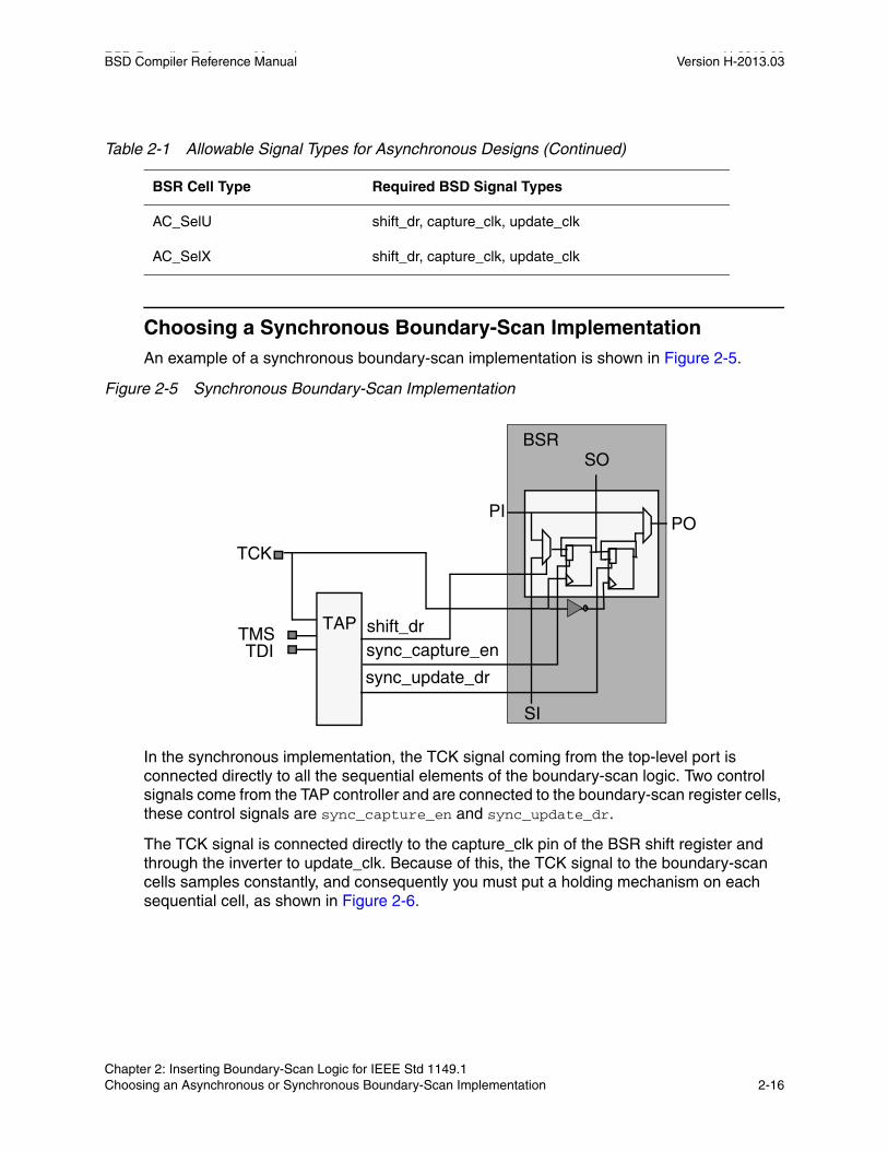
BSD Compiler Reference Manual H-2013.03BSD Compiler Reference Manual Version H-2013.03
Choosing a Synchronous Boundary-Scan ImplementationAn example of a synchronous boundary-scan implementation is shown in Figure 2-5.
Figure 2-5 Synchronous Boundary-Scan Implementation
In the synchronous implementation, the TCK signal coming from the top-level port is connected directly to all the sequential elements of the boundary-scan logic. Two control signals come from the TAP controller and are connected to the boundary-scan register cells, these control signals are sync_capture_en and sync_update_dr.
The TCK signal is connected directly to the capture_clk pin of the BSR shift register and through the inverter to update_clk. Because of this, the TCK signal to the boundary-scan cells samples constantly, and consequently you must put a holding mechanism on each sequential cell, as shown in Figure 2-6.
AC_SelU shift_dr, capture_clk, update_clk
AC_SelX shift_dr, capture_clk, update_clk
Table 2-1 Allowable Signal Types for Asynchronous Designs (Continued)
BSR Cell Type Required BSD Signal Types
TDITMS
TCK
shift_drsync_capture_en
sync_update_dr
TAP
BSR
SI
SO
PIPO
Chapter 2: Inserting Boundary-Scan Logic for IEEE Std 1149.1 Choosing an Asynchronous or Synchronous Boundary-Scan Implementation 2-16

BSD Compiler Reference Manual Version H-2013.03
Figure 2-6 Holding Mechanism for Synchronous Implementation of a BC_4 Cell
Because tck is connected to all the sequential cells, you can build a clock tree and be sure there is no skew between clock tree branches. This allows more reliable timing in the boundary-scan logic. The disadvantage is the consumption of area caused by the holding mechanism required on all sequential cells.
Table 2-2 lists the required signal types for various cell types.
Table 2-2 Allowable Signal Types for Synchronous Designs
BSR Cell Type Required BSD Signal Types
BC_1 in input pad shift_dr, capture_clk, capture_en, update_clk, update_en, mode_in
BC_2 in input pad shift_dr, capture_clk, capture_en, update_clk, update_en, mode_in
BC_1/BC_2 in output pad shift_dr, capture_clk, capture_en, update_clk, update_en, mode_out
BC_4 shift_dr, capture_clk, capture_en
BC_7 shift_dr, capture_clk, capture_en, update_clk, update_en, mode1_inout, mode2_inout
AC_1/AC_2 in output pad shift_dr, capture_clk, capture_en, update_clk, update_en, mode_out, ac_test, ac_mode
D Q0
1
s
tck
capture_en
DFF1data_in
si
shift_dr
so1
0
Chapter 2: Inserting Boundary-Scan Logic for IEEE Std 1149.1 Choosing an Asynchronous or Synchronous Boundary-Scan Implementation 2-17Chapter 2: Inserting Boundary-Scan Logic for IEEE Std 1149.1 Choosing an Asynchronous or Synchronous Boundary-Scan Implementation 2-17

BSD Compiler Reference Manual H-2013.03BSD Compiler Reference Manual Version H-2013.03
Choosing Boundary-Scan Components
When you insert boundary-scan logic, you can use default boundary-scan elements or you can use custom elements. Default elements used by BSD Compiler reside in the DesignWare Foundation Library. Custom components are designs you choose. See the BSD Compiler User Guide for more information on using custom boundary-scan components.
BSD Compiler allows you to use components you design yourself to suit your special needs. For example, you might have special requirements for your boundary-scan logic such as the way you want to implement your boundary-scan register or the way you want to implement your TAP controller. BSD Compiler provides you with the freedom to implement your components in the way you choose. BSD Compiler connects these components automatically, regardless of whether they are custom or default elements.
The process of using custom boundary-scan components for boundary-scan insertion is the same as that for using default components. From outside the component, the boundary-scan elements look exactly the same to BSD Compiler. Consequently, the insertion of default boundary-scan components is the same as the insertion of custom components, except that BSD Compiler uses different references.
Your custom boundary-scan elements and TAP controllers must match the synchronous or asynchronous access interface of the DesignWare foundation components.
Design Requirements for Custom Boundary-Scan Components
The interface requirements for custom boundary-scan components are described in this section. Although BSD Compiler does not deal with the internal representation of the component for the purpose of boundary-scan insertion, compliance checking verifies the IEEE Std 1149.1 compliance of your design components.
If you want to use your design as a custom BSR cell, use the define_dft_design commands. These are discussed in the BSD Compiler User Guide. This command specifies the correspondence between the design pin and the signal type. You must identify the design pin signal type correspondence so that BSD Compiler can make the association.
AC_SelU shift_dr, capture_clk, capture_en, update_clk, update_en
AC_SelX shift_dr, capture_clk, update_clk
Table 2-2 Allowable Signal Types for Synchronous Designs (Continued)
BSR Cell Type Required BSD Signal Types
Chapter 2: Inserting Boundary-Scan Logic for IEEE Std 1149.1 Choosing Boundary-Scan Components 2-18
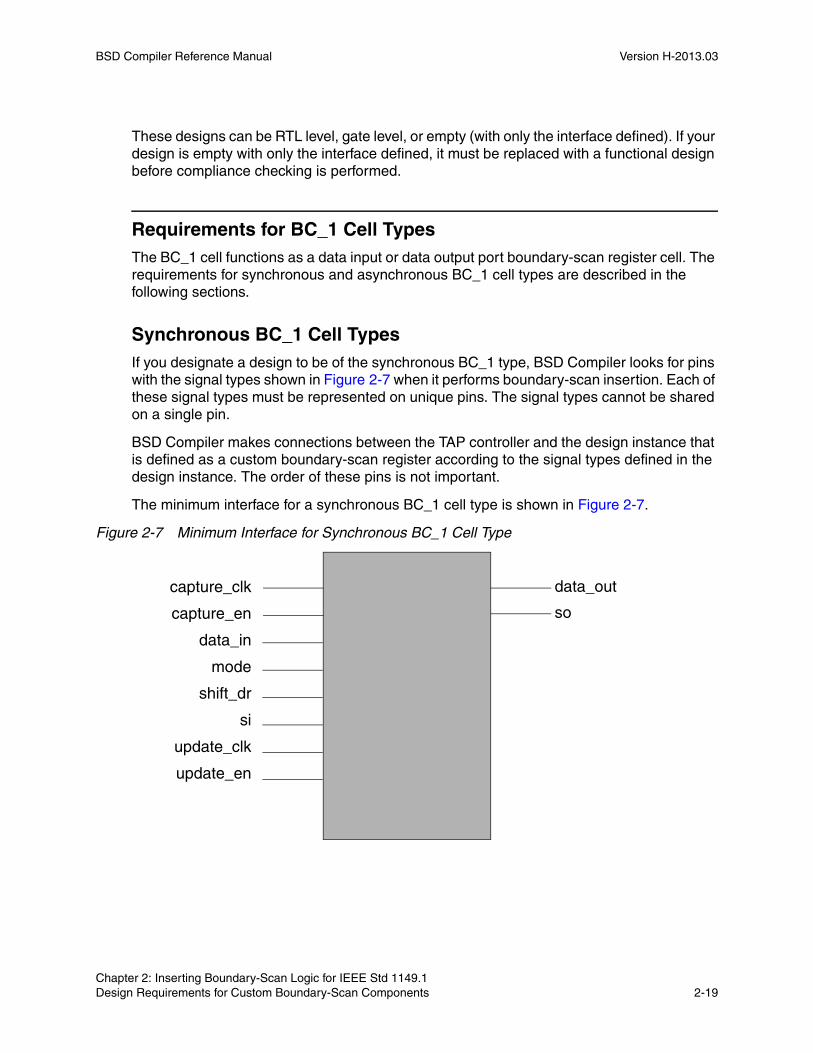
BSD Compiler Reference Manual Version H-2013.03
These designs can be RTL level, gate level, or empty (with only the interface defined). If your design is empty with only the interface defined, it must be replaced with a functional design before compliance checking is performed.
Requirements for BC_1 Cell TypesThe BC_1 cell functions as a data input or data output port boundary-scan register cell. The requirements for synchronous and asynchronous BC_1 cell types are described in the following sections.
Synchronous BC_1 Cell TypesIf you designate a design to be of the synchronous BC_1 type, BSD Compiler looks for pins with the signal types shown in Figure 2-7 when it performs boundary-scan insertion. Each of these signal types must be represented on unique pins. The signal types cannot be shared on a single pin.
BSD Compiler makes connections between the TAP controller and the design instance that is defined as a custom boundary-scan register according to the signal types defined in the design instance. The order of these pins is not important.
The minimum interface for a synchronous BC_1 cell type is shown in Figure 2-7.
Figure 2-7 Minimum Interface for Synchronous BC_1 Cell Type
data_in
mode
shift_dr
si
capture_en
update_en
update_clk
capture_clk data_out
so
Chapter 2: Inserting Boundary-Scan Logic for IEEE Std 1149.1 Design Requirements for Custom Boundary-Scan Components 2-19Chapter 2: Inserting Boundary-Scan Logic for IEEE Std 1149.1 Design Requirements for Custom Boundary-Scan Components 2-19

BSD Compiler Reference Manual H-2013.03BSD Compiler Reference Manual Version H-2013.03
Asynchronous BC_1 Cell TypeIf you designate a design to be of the asynchronous BC_1 type, BSD Compiler looks for pins with the signal types shown in Figure 2-8 when it performs boundary-scan insertion. Each of these signal types must be represented on unique pins, and each must be present on the design. The signal types cannot be shared on a single pin.
BSD Compiler makes connections between the TAP controller and the design instance that is defined as a custom BSR according to the signal types defined in the design instance. The order of these pins is not important.
The minimum interface for an asynchronous BC_1 cell type is shown in Figure 2-8.
Figure 2-8 Minimum Interface for Asynchronous BC_1 Cell Type
Requirements for BC_2 Cell TypesThe BC_2 cell functions as a data input or data output port boundary-scan register cell. The requirements for synchronous and asynchronous BC_2 cell types are described in the following sections.
data_out
sodata_in
mode
shift_dr
si
update_clk
capture_clk
Chapter 2: Inserting Boundary-Scan Logic for IEEE Std 1149.1 Design Requirements for Custom Boundary-Scan Components 2-20

BSD Compiler Reference Manual Version H-2013.03
Synchronous BC_2 Cell TypesIf you designate a design to be of the synchronous BC_2 type, BSD Compiler looks for pins with the signal types shown in Figure 2-9 when it performs boundary-scan insertion. Each of these signal types must be represented on unique pins. The signal types cannot be shared on a single pin.
Although the interfaces for BC_1 and BC_2 cell types are the same, their internal functionality is different. Consequently, the two cell types must be characterized differently.
BSD Compiler makes connections between the TAP controller and the design instance that is defined as a custom BSR according to the signal types defined in the design instance. The order of these pins is not important.
The minimum interface for a synchronous BC_2 cell type is shown in Figure 2-9.
Figure 2-9 Minimum Interface for Synchronous BC_2 Cell Type
Asynchronous BC_2 Cell TypeIf you designate a design to be of the asynchronous BC_2 type, BSD Compiler looks for pins with the signal types shown in Figure 2-10 when it performs boundary-scan insertion. Each of these signal types must be represented on unique pins, and each must be present on the design. The signal types cannot be shared on a single pin.
BSD Compiler makes connections between the TAP controller and the design instance that is defined as a custom BSR according to the signal types defined in the design instance. The order of these pins is not important.
data_in
mode
shift_dr
si
capture_en
update_en
update_clk
capture_clk data_out
so
Chapter 2: Inserting Boundary-Scan Logic for IEEE Std 1149.1 Design Requirements for Custom Boundary-Scan Components 2-21Chapter 2: Inserting Boundary-Scan Logic for IEEE Std 1149.1 Design Requirements for Custom Boundary-Scan Components 2-21
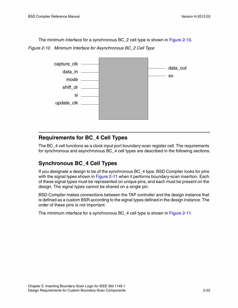
BSD Compiler Reference Manual H-2013.03BSD Compiler Reference Manual Version H-2013.03
The minimum interface for a synchronous BC_2 cell type is shown in Figure 2-10.
Figure 2-10 Minimum Interface for Asynchronous BC_2 Cell Type
Requirements for BC_4 Cell TypesThe BC_4 cell functions as a clock input port boundary-scan register cell. The requirements for synchronous and asynchronous BC_4 cell types are described in the following sections.
Synchronous BC_4 Cell TypesIf you designate a design to be of the synchronous BC_4 type, BSD Compiler looks for pins with the signal types shown in Figure 2-11 when it performs boundary-scan insertion. Each of these signal types must be represented on unique pins, and each must be present on the design. The signal types cannot be shared on a single pin.
BSD Compiler makes connections between the TAP controller and the design instance that is defined as a custom BSR according to the signal types defined in the design instance. The order of these pins is not important.
The minimum interface for a synchronous BC_4 cell type is shown in Figure 2-11.
data_out
sodata_in
mode
shift_dr
si
update_clk
capture_clk
Chapter 2: Inserting Boundary-Scan Logic for IEEE Std 1149.1 Design Requirements for Custom Boundary-Scan Components 2-22
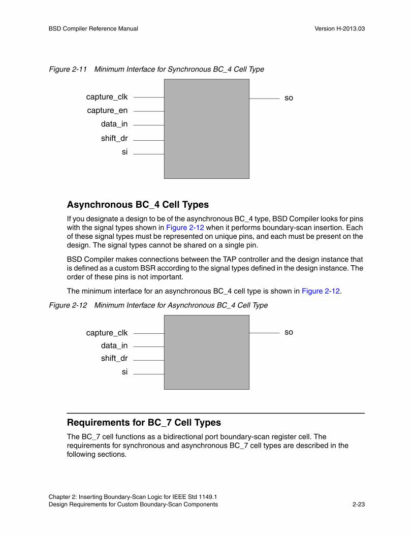
BSD Compiler Reference Manual Version H-2013.03
Figure 2-11 Minimum Interface for Synchronous BC_4 Cell Type
Asynchronous BC_4 Cell TypesIf you designate a design to be of the asynchronous BC_4 type, BSD Compiler looks for pins with the signal types shown in Figure 2-12 when it performs boundary-scan insertion. Each of these signal types must be represented on unique pins, and each must be present on the design. The signal types cannot be shared on a single pin.
BSD Compiler makes connections between the TAP controller and the design instance that is defined as a custom BSR according to the signal types defined in the design instance. The order of these pins is not important.
The minimum interface for an asynchronous BC_4 cell type is shown in Figure 2-12.
Figure 2-12 Minimum Interface for Asynchronous BC_4 Cell Type
Requirements for BC_7 Cell TypesThe BC_7 cell functions as a bidirectional port boundary-scan register cell. The requirements for synchronous and asynchronous BC_7 cell types are described in the following sections.
data_in
shift_dr
si
capture_en
capture_clk so
data_in
shift_dr
si
capture_clk so
Chapter 2: Inserting Boundary-Scan Logic for IEEE Std 1149.1 Design Requirements for Custom Boundary-Scan Components 2-23Chapter 2: Inserting Boundary-Scan Logic for IEEE Std 1149.1 Design Requirements for Custom Boundary-Scan Components 2-23
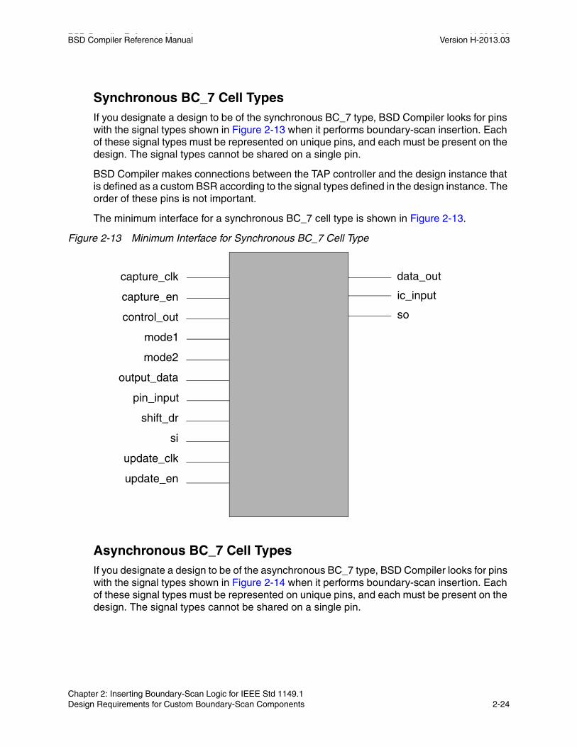
BSD Compiler Reference Manual H-2013.03BSD Compiler Reference Manual Version H-2013.03
Synchronous BC_7 Cell TypesIf you designate a design to be of the synchronous BC_7 type, BSD Compiler looks for pins with the signal types shown in Figure 2-13 when it performs boundary-scan insertion. Each of these signal types must be represented on unique pins, and each must be present on the design. The signal types cannot be shared on a single pin.
BSD Compiler makes connections between the TAP controller and the design instance that is defined as a custom BSR according to the signal types defined in the design instance. The order of these pins is not important.
The minimum interface for a synchronous BC_7 cell type is shown in Figure 2-13.
Figure 2-13 Minimum Interface for Synchronous BC_7 Cell Type
Asynchronous BC_7 Cell TypesIf you designate a design to be of the asynchronous BC_7 type, BSD Compiler looks for pins with the signal types shown in Figure 2-14 when it performs boundary-scan insertion. Each of these signal types must be represented on unique pins, and each must be present on the design. The signal types cannot be shared on a single pin.
mode1
mode2
shift_dr
si
capture_en
update_en
update_clk
capture_clk data_out
ic_input
control_out
output_data
pin_input
so
Chapter 2: Inserting Boundary-Scan Logic for IEEE Std 1149.1 Design Requirements for Custom Boundary-Scan Components 2-24

BSD Compiler Reference Manual Version H-2013.03
BSD Compiler makes connections between the TAP controller and the design instance that is defined as a custom BSR according to the signal types defined in the design instance. The order of these pins is not important.
The minimum interface for an asynchronous BC_7 cell type is shown in Figure 2-14.
Figure 2-14 Minimum Interface for Asynchronous BC_7 Cell Type
TAP Controller Interface RequirementsAlthough you are not required to have the complete functional design when you implement the TAP controller, be careful about what you implement and how you implement it. BSD Compiler checks the TAP controller implementation during compliance checking. Make sure your design is compliant before you move to the compliance checking phase.
Note: The instruction register and BYPASS register should be part of the design declared at the TAP controller. The TAP controller interface must provide a signal to select the BYPASS register.
Use the DW_tap_uc controller. For details about the DW_tap_uc controller, refer to the Synopsys Design Ware datasheet, DW_tap_uc TAP Controller with USERCODE Support.
Figure 2-15 shows the TAP controller interface diagram for the default DW_tap_uc controller.
mode1
mode2
shift_dr
si
update_clk
capture_clk data_out
ic_inputcontrol_out
output_data
pin_input
so
Chapter 2: Inserting Boundary-Scan Logic for IEEE Std 1149.1 Design Requirements for Custom Boundary-Scan Components 2-25Chapter 2: Inserting Boundary-Scan Logic for IEEE Std 1149.1 Design Requirements for Custom Boundary-Scan Components 2-25

BSD Compiler Reference Manual H-2013.03BSD Compiler Reference Manual Version H-2013.03
Figure 2-15 TAP Controller Interface Diagram for the DW_tap_uc Controller
tdo
tdo_en
instructions
tap_state [15 : 0]
tms
tck
trst_n
tdi
so
mux_select
so from BSR
mnfr_id
bypass_sel
User-defined instr.
input pads
so from TDRs
BSR = boundary scan registerTDR = test data register
Instructions that select these registers as the serial path between tdi and tdo
HIGHZCLAMP
clock_drshift_drupdate_dr
sync_update_dr
DW_tap_uc
to BSR and
sync_capture_en
Data Serial PathMux
Instruction Decode Block
user_code_sel
device_id_sel
user_code_val
ver_sel
part_num
BYPASS
TDRs
part_num_sel
mnfr_id_sel
sentinel_val
test
ver
Controller
Chapter 2: Inserting Boundary-Scan Logic for IEEE Std 1149.1 Design Requirements for Custom Boundary-Scan Components 2-26

BSD Compiler Reference Manual Version H-2013.03
Table 2-3 describes the pins associated with DW_tap_uc:
Table 2-3 DW_tap_uc Pin Description
Pin name Size Type Function
tck 1 Input Test clock
trst_n 1 Input Test reset, active low
tms 1 Input Test mode select
tdi 1 Input Test data in
so 1 Input Serial data from boundary scan register and data registers
bypass_sel 1 Input Selects the bypass register, active high
sentinel_val width - 1 Input User-defined status bits
device_id_sel 1 Input Selects the device identification register, active high
user_code_sel 1 Input Selects the user_code_val bus for input into the device identification register, active high
user_code_val 32 Input 32-bit user-defined code
ver 4 Input 4-bit version number
ver_sel 1 Input Selects version from the parameter or the ver input port, where 0 = version (parameter) and 1 = ver (input port)
part_num 16 Input 16-bit part number
part_num_sel 1 Input Selects part from the parameter or the part_num from the input port, where 0 = part (parameter) and 1 = part_num (input port)
mnfr_id 11 Input 11-bit JEDEC manufacturer’s identity code (mnfr_id not equal to 127)
Chapter 2: Inserting Boundary-Scan Logic for IEEE Std 1149.1 Design Requirements for Custom Boundary-Scan Components 2-27Chapter 2: Inserting Boundary-Scan Logic for IEEE Std 1149.1 Design Requirements for Custom Boundary-Scan Components 2-27
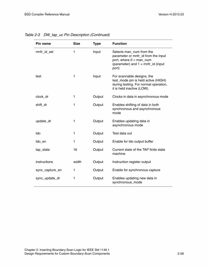
BSD Compiler Reference Manual H-2013.03BSD Compiler Reference Manual Version H-2013.03
mnfr_id_sel 1 Input Selects man_num from the parameter or mnfr_id from the input port, where 0 = man_num (parameter) and 1 = mnfr_id (input port)
test 1 Input For scannable designs, the test_mode pin is held active (HIGH) during testing. For normal operation, it is held inactive (LOW).
clock_dr 1 Output Clocks in data in asynchronous mode
shift_dr 1 Output Enables shifting of data in both synchronous and asynchronous mode
update_dr 1 Output Enables updating data in asynchronous mode
tdo 1 Output Test data out
tdo_en 1 Output Enable for tdo output buffer
tap_state 16 Output Current state of the TAP finite state machine
instructions width Output Instruction register output
sync_capture_en 1 Output Enable for synchronous capture
sync_update_dr 1 Output Enables updating new data in synchronous_mode
Table 2-3 DW_tap_uc Pin Description (Continued)
Pin name Size Type Function
Chapter 2: Inserting Boundary-Scan Logic for IEEE Std 1149.1 Design Requirements for Custom Boundary-Scan Components 2-28

BSD Compiler Reference Manual Version H-2013.03
Table 2-4 describes the parameters associated with DW_tap_uc:
Note: The sentinel_val pins are TAP port input pins used to monitor a bit status from a user-defined register or any other design bit such as the FAIL or DONE bits of the BIST controller. BSD Compiler derives a 1-N number of signals from the total number of IR register bits. The connections to the status bits must be done manually. For example, in the case of the BIST controller, you can connect the FAIL bits directly from the BIST controller to the sentinal_val signals.
Introduction to DW_tap_ucFeatures and benefits of using the TAP controller are as follows:
• IEEE Std 1149.1 compliant
• Synchronous or asynchronous registers with respect to tck
Table 2-4 DW_tap_uc Parameter Description
Parameter Values Description
width 2 to 32 Default = 2
Width of instruction register
id 0 or 1 Default = 0
Determines whether the device identification register is present, where 0 = not present and 1 = present
idcode_ opcode
1 to 2width-1 Default = 1
Opcode for IDCODE
version 0 to 15 Default = 0
4-bit version number
part 0 to 65535 Default = 0
16-bit part number
man_num 0 to 2047 man_num not equal to 127 Default = 0
11-bit JEDEC manufacturer identity code
sync_mode 0 or 1 Default = 0
Determines if the bypass, device identification, and instruction registers are synchronous with respect to tck, where 0 = asynchronous and 1 = synchronous
Chapter 2: Inserting Boundary-Scan Logic for IEEE Std 1149.1 Design Requirements for Custom Boundary-Scan Components 2-29Chapter 2: Inserting Boundary-Scan Logic for IEEE Std 1149.1 Design Requirements for Custom Boundary-Scan Components 2-29
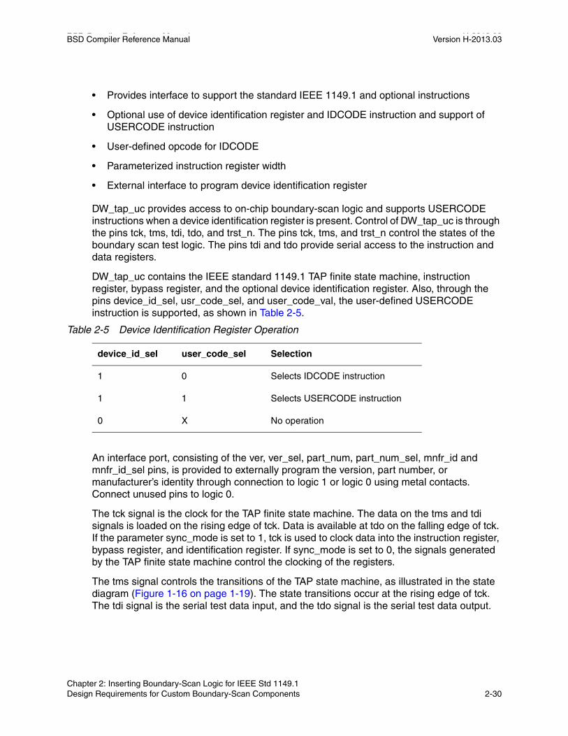
BSD Compiler Reference Manual H-2013.03BSD Compiler Reference Manual Version H-2013.03
• Provides interface to support the standard IEEE 1149.1 and optional instructions
• Optional use of device identification register and IDCODE instruction and support of USERCODE instruction
• User-defined opcode for IDCODE
• Parameterized instruction register width
• External interface to program device identification register
DW_tap_uc provides access to on-chip boundary-scan logic and supports USERCODE instructions when a device identification register is present. Control of DW_tap_uc is through the pins tck, tms, tdi, tdo, and trst_n. The pins tck, tms, and trst_n control the states of the boundary scan test logic. The pins tdi and tdo provide serial access to the instruction and data registers.
DW_tap_uc contains the IEEE standard 1149.1 TAP finite state machine, instruction register, bypass register, and the optional device identification register. Also, through the pins device_id_sel, usr_code_sel, and user_code_val, the user-defined USERCODE instruction is supported, as shown in Table 2-5.
An interface port, consisting of the ver, ver_sel, part_num, part_num_sel, mnfr_id and mnfr_id_sel pins, is provided to externally program the version, part number, or manufacturer’s identity through connection to logic 1 or logic 0 using metal contacts. Connect unused pins to logic 0.
The tck signal is the clock for the TAP finite state machine. The data on the tms and tdi signals is loaded on the rising edge of tck. Data is available at tdo on the falling edge of tck. If the parameter sync_mode is set to 1, tck is used to clock data into the instruction register, bypass register, and identification register. If sync_mode is set to 0, the signals generated by the TAP finite state machine control the clocking of the registers.
The tms signal controls the transitions of the TAP state machine, as illustrated in the state diagram (Figure 1-16 on page 1-19). The state transitions occur at the rising edge of tck. The tdi signal is the serial test data input, and the tdo signal is the serial test data output.
Table 2-5 Device Identification Register Operation
device_id_sel user_code_sel Selection
1 0 Selects IDCODE instruction
1 1 Selects USERCODE instruction
0 X No operation
Chapter 2: Inserting Boundary-Scan Logic for IEEE Std 1149.1 Design Requirements for Custom Boundary-Scan Components 2-30

BSD Compiler Reference Manual Version H-2013.03
The trst_n signal is an active low signal that asynchronously resets the TAP state machine to the Test-Logic-Reset state.
The DW_tap_uc output signals clock_dr, shift_dr, update_dr, sync_update_dr, and sync_capture_en control the boundary-scan cells. In synchronous mode, boundary scan cells are updated on the rising edge to tck.
The tap_state port provides access to the one-hot encoded TAP state machine, enabling advanced users to construct add-on circuits.
Synchronous TAP ControllerThe mandatory interface for a synchronous TAP controller is listed in Figure 2-16.
Figure 2-16 Minimum Interface for Synchronous TAP Controller Type
The sync_capture_en signal is the enable for data clocked into the capture stage of the BSR cell.
The sync_update_dr signal is the clock that allows data to move from one stage to another. In the synchronous TAP controller implementation you have to use both capture_clk and sync_capture_en signals to allow data to move to the capture stage.
For more information on the TAP controller see “Inserting the TAP Controller” on page 2-47.
Asynchronous TAP ControllerThe mandatory interface for an asynchronous TAP controller is shown in Figure 2-17.
bypass_sel
so
tck
tdi
tms
shift_dr
sync_capture_en
sync_update_dr
tdo
tdo_en
trst_n
instructions
Chapter 2: Inserting Boundary-Scan Logic for IEEE Std 1149.1 Design Requirements for Custom Boundary-Scan Components 2-31Chapter 2: Inserting Boundary-Scan Logic for IEEE Std 1149.1 Design Requirements for Custom Boundary-Scan Components 2-31

BSD Compiler Reference Manual H-2013.03BSD Compiler Reference Manual Version H-2013.03
Figure 2-17 Minimum Interface for Asynchronous TAP Controller Type
Inserting Boundary-Scan Logic
You insert boundary-scan logic into your design by using the insert_dft command. See the BSD Compiler User Guide for a detailed discussion of this command. This command is not incremental. You can only insert boundary-scan logic one time. You should not insert boundary-scan logic until you are confident your design is ready for it. BSD Compiler has preview mechanisms that allow you to judge the readiness of your design for boundary-scan logic. See “Previewing Your Boundary-Scan Design” on page 2-61.
According to your implementation choice, BSD Compiler will pick either the synchronous version or the asynchronous version of the boundary-scan components. If you make no specification, BSD Compiler chooses synchronous for you.
The sections that follow describe the steps insert_dft follows to generate boundary-scan logic.
Analyzing PortsBefore it inserts boundary-scan logic into the design, insert_dft analyzes each port and the pad to which it is connected.
Through this analysis, insert_dft automatically identifies the following ports:
• Linkage ports
• Nonclock input ports
• Clock ports
bypass_sel
so
tck
tdi
tms
clock_dr
shift_dr
tdo_en
update_dr
tdotrst_n
instructions
Chapter 2: Inserting Boundary-Scan Logic for IEEE Std 1149.1 Inserting Boundary-Scan Logic 2-32
BSD Compiler Reference Manual Version H-2013.03
• Two-state output ports
• Tristate output ports
• Bidirectional ports
• Open drain
• Open source
Degenerated bidirectional ports acting as tristate output ports are handled automatically. Linkage ports are excluded from the set of ports that have boundary-scan registers inserted.
Handling Global-Enable PinsIf insert_dft detects a tristate output driver with more than one enable pin and if the other enable pins are driven from a top-level port, it recognizes the top-level enable pins as global-enable pins. The insert_dft command inserts disabling logic on global-enable pins to make these signals inactive during boundary-scan testing.
When the TAP controller is not in the Test-Logic-Reset state, or while the TRST* port remains at logic 1, the global-enable signal does not affect the behavior of the circuit.
Because BSD Compiler disables global-enable pins during boundary-scan testing, there is no need to define a tristate output driver with global-enable pins as a compliance-enable port. In this way, compliance checking can be performed without problems. See Figure 2-18 for an example of a global-enable signal.
Chapter 2: Inserting Boundary-Scan Logic for IEEE Std 1149.1 Inserting Boundary-Scan Logic 2-33Chapter 2: Inserting Boundary-Scan Logic for IEEE Std 1149.1 Inserting Boundary-Scan Logic 2-33

BSD Compiler Reference Manual H-2013.03BSD Compiler Reference Manual Version H-2013.03
Figure 2-18 Global-Enable Pin
Inserting Boundary-Scan Register CellsBy using the information extracted during the port analysis step, the insert_dft command puts a BSR cell on each nonlinkage port it discovers. The BSR cell inserted into the design by insert_dft is, by default, a DesignWare Foundation Library element. It can also be a user-defined component. These components can be synchronous or asynchronous BSR cell implementations. The sections that follow describe the default behavior of insert_dft.
Inserting Input Port Boundary-Scan Register CellsUsing boundary-scan components in the DesignWare Foundation Library, insert_dft places BC_2 BSR cells on nonclock input ports.
An example of a BC_2 BSR cell on an input port is shown in Figure 2-19.
DW_tap_uc
Chapter 2: Inserting Boundary-Scan Logic for IEEE Std 1149.1 Inserting Boundary-Scan Logic 2-34

BSD Compiler Reference Manual Version H-2013.03
Figure 2-19 Synchronous DesignWare BC_2 BSR Cell on Input Ports
Table 2-6 provides specific pin description information for the BC_2 cell.
Table 2-6 BC_2 Pin Description
Pin name Size Type Function
capture_clk 1 Input Clocks data into the capture stage
update_clk 1 Input Clocks data into the update stage
capture_en 1 Input Enable for data clocked into the capture stage, active low
update_en 1 Input Enable for data clocked into the update stage, active high
shift_dr 1 Input Enables the boundary-scan chain to shift data one stage toward its serial output (tdo)
D Q0
1
s
D Q0
1s
0
1s
0
1s
capture_clk
mode
data_indata_out
SO
SI
shift_dr
capture_en
update_en
update_clk
DFF1 DFF2
Chapter 2: Inserting Boundary-Scan Logic for IEEE Std 1149.1 Inserting Boundary-Scan Logic 2-35Chapter 2: Inserting Boundary-Scan Logic for IEEE Std 1149.1 Inserting Boundary-Scan Logic 2-35

BSD Compiler Reference Manual H-2013.03BSD Compiler Reference Manual Version H-2013.03
The advantage of using a BC_2 type BSR cell on an input is its testability. The multiplexer (MUX) logic, U3, selecting between the latched output (DFF2) and the parallel input (PI) can be tested by capturing the signal into the shift register.
Inserting Clock Input Port Boundary-Scan Register CellsUsing boundary-scan components in the DesignWare Foundation Library, insert_dft places BC_4 BSR cells on clock-input ports.
An example of a BC_4 cell on a clock port is shown in Figure 2-20.
Figure 2-20 Synchronous DesignWare BC_4 BSR Cell on Clock Ports
mode 1 Input Determines whether data_out is controlled by the boundary-scan cell or by the data_in signal
si 1 Input Serial path from the previous boundary-scan cell
data_in 1 Input Input data
data_out 1 Output Output data
so 1 Output Serial path to the next boundary-scan cell
Table 2-6 BC_2 Pin Description (Continued)
Pin name Size Type Function
D Q0
1
s
0
1s
data_in
SI
shift_dr
capture_en
capture_clk
SO
DFF1
Chapter 2: Inserting Boundary-Scan Logic for IEEE Std 1149.1 Inserting Boundary-Scan Logic 2-36

BSD Compiler Reference Manual Version H-2013.03
Table 2-7 provides specific pin description information for the BC_4 cell.
A BC_4, which is an observe-only BSR cell, is selected for the clock input to minimize the timing impact of the BSR cell on the clock network.
Inserting Two-State Output Port Boundary-Scan Register CellsThe cell type BC_1 is used as a BSR cell for a two-state output port. It uses the DesignWare Foundation Library component BC_1.
Figure 2-21 shows an example of a BC_1 BSR cell placed on an output port.
Table 2-7 BC_4 Pin Description
Pin Name Size Type Function
capture_clk 1 Input Clocks data into the capture stage
capture_en 1 Input Enable for data clocked into the capture stage, active low
shift_dr 1 Input Enables the boundary-scan chain to shift data one stage toward its serial output (tdo)
si 1 Input Serial path from the previous boundary-scan cell
data_in 1 Input Input data
so 1 Output Serial path to the next boundary-scan cell
Chapter 2: Inserting Boundary-Scan Logic for IEEE Std 1149.1 Inserting Boundary-Scan Logic 2-37Chapter 2: Inserting Boundary-Scan Logic for IEEE Std 1149.1 Inserting Boundary-Scan Logic 2-37

BSD Compiler Reference Manual H-2013.03BSD Compiler Reference Manual Version H-2013.03
Figure 2-21 Synchronous DesignWare BC_1 BSR Cell on Output Port
Table 2-8 provides specific pin description information for the BC_1 cell.
Table 2-8 BC_1 Pin Description
Pin Name Size Type Function
capture_clk 1 Input Clocks data into the capture stage
update_clk 1 Input Clocks data into the update stage
capture_en 1 Input Enable for data clocked into the capture stage, active low
update_en 1 Input Enable for data clocked into the update stage, active high
shift_dr 1 Input Enables the boundary-scan chain to shift data one stage toward its serial output (tdo)
mode 1 Input Determines whether data_out is controlled by the boundary-scan cell or by the data_in signal
update_clk
D Q1
0s
D Q1
0
s
0
1s
0
1s
data_in
SI
shift_dr
capture_en
capture_clk
update_en
mode
data_out
SO
DFF1DFF2
Chapter 2: Inserting Boundary-Scan Logic for IEEE Std 1149.1 Inserting Boundary-Scan Logic 2-38

BSD Compiler Reference Manual Version H-2013.03
Inserting Tristate Output Port Boundary-Scan Register CellsBSD Compiler inserts data and control cells on each tristate output port. For each degenerated bidirectional port in output only mode, only data cells are inserted. The control BSR cell is a BC_2. The data BSR cell is a BC_1. This implementation uses the DesignWare Foundation Library components BC_2 and BC_1. This implementation provides one control cell for every tristate enable output port. This prevents the problems associated with ground bounce and allows the board-level test vector software to activate one tristate output at a time, reducing the noise generated by the transition. You can share the enable signal between several tristate output ports by using the merging capabilities of optimization. See “Merging Boundary-Scan Register Cells” on page 2-62 for more information.
Inserting Bidirectional Port CellsConsider a bidirectional data BSR cell and a control BSR cell for each nondegenerated bidirectional port. The control BSR cell is a BC_2 and the data BSR cell is a BC_7. They use the DesignWare Foundation Library components BC_2 and BC_7. An example of a BC_7 cell used as a bidirectional port is shown in Figure 2-22.
si 1 Input Serial path from the previous boundary-scan cell
data_in 1 Input Input data
data_out 1 Output Output data
so 1 Output Serial path to the next boundary-scan cell
Table 2-8 BC_1 Pin Description (Continued)
Pin Name Size Type Function
Chapter 2: Inserting Boundary-Scan Logic for IEEE Std 1149.1 Inserting Boundary-Scan Logic 2-39Chapter 2: Inserting Boundary-Scan Logic for IEEE Std 1149.1 Inserting Boundary-Scan Logic 2-39

BSD Compiler Reference Manual H-2013.03BSD Compiler Reference Manual Version H-2013.03
t
Figure 2-22 Synchronous DesignWare BC_7 BSR Cell on a Bidirectional Port
Table 2-9 provides specific pin description information for the BC_7 cell.
Table 2-9 BC_7 Pin Description
Pin Name Size Type Function
capture_clk 1 Input Clocks data into the capture stage
update_clk 1 Input Clocks data into the update stage
capture_en 1 Input Enable for data clocked into the capture stage, active low
D Q0
1
s
D Q0
1s
0
1s
0
1s
0
1s
0
1s
&
capture_clk
update_clk
output_data
mode_1
pin_input
SI
shift_dr
mode_2
control_out
capture_en
update_en
data_ou
SO
ic_input
DFF1DFF2
Chapter 2: Inserting Boundary-Scan Logic for IEEE Std 1149.1 Inserting Boundary-Scan Logic 2-40
BSD Compiler Reference Manual Version H-2013.03
Naming Conventions for Boundary-Scan Register CellsBSD Compiler uses a naming convention for boundary-scan register cells. The convention associates the boundary-scan register cell’s name with the name of the design to which it belongs, its corresponding port name, and its relative position in the boundary-scan chain.
The instance name of a given boundary-scan register cell is then
top_level_design_name_port_name_bsr index
For example, if the boundary-scan cell is part of the design MyTop, and its associated port name is IN[28], and its position in the chain is 167, its instance name becomes
MyTop_IN[28]_bsr167
update_en 1 Input Enable for data clocked into the update stage, active high
shift_dr 1 Input Enables the boundary-scan chain to shift data one stage toward its serial output (tdo)
mode 1 1 Input Determines whether data_out is controlled by the boundary-scan cell or by the data_in signal
mode 2 1 Input Determines whether ic_input is controlled by the boundary-scan cell or by the output_data signal
si 1 Input Serial path from the previous boundary-scan cell
pin_input 1 Input IC system input pin
control_out 1 Input Control signal for the output enable
output_data 1 Input IC output logic signal
ic_input 1 Output IC input logic signal
data_out 1 Output Output data
so 1 Output Serial path to the next boundary-scan cell
Table 2-9 BC_7 Pin Description (Continued)
Pin Name Size Type Function
Chapter 2: Inserting Boundary-Scan Logic for IEEE Std 1149.1 Inserting Boundary-Scan Logic 2-41Chapter 2: Inserting Boundary-Scan Logic for IEEE Std 1149.1 Inserting Boundary-Scan Logic 2-41
BSD Compiler Reference Manual H-2013.03BSD Compiler Reference Manual Version H-2013.03
Grouping BSR CellsThe insert_dft command groups all the BSR cells under the same level of hierarchy. The instance name of this block is called, by convention,
name_of_the_top_level_design_BSR_top_inst
The design name thus becomes
name_of_the_top_level_design_BSR_top_inst_design
Because the naming convention associates the design, port, and index name, it is very easy to group them at your convenience to fit any requirements for your design hierarchy.
The Design Compiler environment provides two commands that allow you to work on the hierarchical gathering and expanding your cells:
• group
• ungroup
When you use these commands with filtering commands, you can customize your boundary-scan hierarchy.
See the Design Compiler documentation for more information on the group and ungroup commands.
Warning: Make sure that each BSR cell remains in one block to allow correct processing during boundary-scan optimization. Consequently, avoid using the following commands on boundary-scan register cells:
ungroup -all -flatten
ungroup DW_bc_* design
Synthesizing the DesignAfter generating the boundary-scan design, the insert_dft command synthesizes the design, which consists of mapping all inserted boundary-scan logic.
Synthesis assumes that your design contains pad cells, core logic, and boundary-scan logic. The pad cells are gate-level representations of pads, or library cells. The boundary-scan logic, however, might still be generic representations. The generic representations of the boundary-scan logic are synthesized so that they are mapped to logic libraries.
During synthesis, BSD Compiler compiles the boundary-scan logic in a bottom-up strategy, which means that each DesignWare module segment is compiled separately and the compiled module is instantiated as required.
Chapter 2: Inserting Boundary-Scan Logic for IEEE Std 1149.1 Inserting Boundary-Scan Logic 2-42

BSD Compiler Reference Manual Version H-2013.03
The Effect of Boundary-Scan Register Cell Type Specifications
After you specify boundary-scan register cell types by using the set_boundary_cell command, BSD Compiler selects the corresponding cells to be connected to each port. This process is dependent on the type of the port that is to be connected to the boundary-scan cell. There are specific types of cells that are allowed on inputs, outputs, and bidirectional ports.
Note: If you know that a port is not digital and you don’t want a BSR inserted on it, use the set_bsd_linkage_port command. See the section “Identifying Linkage Ports” on page 2-11 for more information.
The sections that follow describe how BSD Compiler uses the cell type specifications you set with the set_boundary_cell command. See the BSD Compiler User Guide for more information on these commands.
The commands you use to specify your boundary-scan register are independent of the type of cell you specify. That means you can use these commands for both default and custom cell specifications.
BSR Cell Types Allowed on Input PortsThe options for BSR cells declared by the set_boundary_cell command that are allowed on input ports are
• BC_1
• BC_2
• BC_4
• BC_7
• none
If you are unfamiliar with these cell types, see “Boundary-Scan Cells” on page 1-27.
After you specify the boundary-scan cell type, BSD Compiler automatically hooks up all the control and data signals of the corresponding BSR.
If you specify none, you can prevent the insertion of boundary-scan cells on a given port. You might do this if you prefer to use a linkage bit for ports that are excluded from boundary-scan testing.
Chapter 2: Inserting Boundary-Scan Logic for IEEE Std 1149.1 The Effect of Boundary-Scan Register Cell Type Specifications 2-43Chapter 2: Inserting Boundary-Scan Logic for IEEE Std 1149.1 The Effect of Boundary-Scan Register Cell Type Specifications 2-43

BSD Compiler Reference Manual H-2013.03BSD Compiler Reference Manual Version H-2013.03
Note: You do not have to specify none if you have used the set_bsd_linkage_port command. This command automatically prevents the insertion of boundary-scan cells on linkage ports.
BSR Cell Types Allowed on Output Ports and Tristate Output PortsThe types of BSR cells declared by the set_boundary_cell command that are allowed on output ports are
• BC_1
• BC_2 (only if INTEST is not implemented in your design)
• none
If you are unfamiliar with these cell types, see “Boundary-Scan Cells” on page 1-27.
After you specify the boundary-scan cell type, BSD Compiler automatically hooks up all the control and data signals of the corresponding BSR.
If you specify none, you can prevent the insertion of boundary-scan cells on a given port.
Note: You do not have to specify none if you have used the set_bsd_linkage_port command. This command automatically prevents the insertion of boundary-scan cells on linkage ports.
BSR Cell Types Allowed for Control CellsThe types of BSR cells declared by the set_boundary_cell command that are accepted on control cells are
• BC_1
• BC_2
• none
There is not a one-to-one correspondence between ports and control cells.
BSD Compiler looks at the port list specified by the command set_boundary_cell to identify what tristate output ports share the control cell together.
If you specify none, you can prevent the insertion of boundary-scan cells on a given control cell.
Chapter 2: Inserting Boundary-Scan Logic for IEEE Std 1149.1 The Effect of Boundary-Scan Register Cell Type Specifications 2-44

BSD Compiler Reference Manual Version H-2013.03
Optimization never increases the number of control cells in the boundary-scan register. By specifying control cells with this command, you can ensure you won’t get more control cells than you want. By using this command, you specify the maximum configuration of control cells. If you want more information about the effect of optimization on this command, see the BSD Compiler User Guide.
BSR Cell Types Allowed for Bidirectional PortsIf you do not specify a direction for a bidirectional cell, you can only use a BC_7 cell on a bidirectional port. If you choose to split the cells to allow both input and output directions, you can use the cells appropriate for input and output ports, respectively.
See the sections on input and output cell types earlier in this chapter for more information.
Ordering Boundary-Scan Register Cells
By default, the BSR cells are ordered in one boundary-scan chain that follows the alphabetical order of the port names given in the design port definition, to which they are linked.
You can use a port-to-pin mapping file to force insert_dft to use a different port order than that provided in the default method. The port-to-pin mapping file performs the following two tasks:
• The correspondence between logical port and physical pin
• The routing order of the cells in your boundary-scan register
Although the port-to-pin mapping file orders the boundary-scan register cells, the file does not indicate the exact position of the control cells in the boundary-scan register. You might want to have more control over this ordering. The set_scan_path command allows you to explicitly specify the positions of data and control cells. If a control cell’s position is not explicitly specified by the set_scan_path command, by default, the control cell is placed before the data cell it controls.
For information on the use of the set_scan_path command, see the BSD Compiler User Guide.
The routing of the BSR conforms exactly to the order specified by the set_scan_path command. The order specified by set_scan_path supersedes the read_pin_map command.
The design for boundary-scan chain order is shown in Figure 2-23.
Chapter 2: Inserting Boundary-Scan Logic for IEEE Std 1149.1 Ordering Boundary-Scan Register Cells 2-45Chapter 2: Inserting Boundary-Scan Logic for IEEE Std 1149.1 Ordering Boundary-Scan Register Cells 2-45

BSD Compiler Reference Manual H-2013.03BSD Compiler Reference Manual Version H-2013.03
Figure 2-23 Design for Boundary-Scan Chain Order
As shown in Example 2-7, you can use the read_pin_map command to specify the initial boundary-scan order.
Example 2-7 Sample Port-to-Pin Mapping File
%> read_pin_map pin.txt
/*pin.txt*/
PACKAGE insert_my_package;
PORT = tdi; PIN = P1;PORT = out1; PIN = P2;PORT = in2; PIN = P3;PORT = in1; PIN = P4;PORT = out2; PIN = P5;PORT = tdo; PIN = P6;
Figure 2-24 shows the resulting boundary-cell chain ordering corresponding to the port-to-pin map of Example 2-7.
Figure 2-24 Boundary-Scan Register Port Ordering With Port-to-Pin Map
In this example, the control cell need not be specified in the pin-to-map file. By default, the control cell is placed before the data port.
in00
in01
out00
out01
ctl2ctl1 in2 in1 TDOTDI out1 out2
Chapter 2: Inserting Boundary-Scan Logic for IEEE Std 1149.1 Ordering Boundary-Scan Register Cells 2-46

BSD Compiler Reference Manual Version H-2013.03
You can fine-tune the boundary-cell chain order by using the set_scan_path command in the following way:
set_scan_path boundary -class bsd \ -ordered_elements [list out1 ctl1 in2 in1 ctl2]
The tool places the ctl1 and ctl2 boundary-scan cells after the data cell after the set_scan_path command is run. The resulting boundary-cell chain ordering is shown in Figure 2-25.
Figure 2-25 Boundary-Scan Register Port Ordering With set_scan_path
See the BSD Compiler User Guide for a detailed discussion on creating the port-to-pin mapping file and using the set_scan_path command.
Inserting the TAP Controller
The default TAP controller is defined by the DesignWare Foundation Library component DW_tap_uc. This component contains
• A 16-bit FSM TAP controller with a one-hot encoding scheme
• A bypass register
• An instruction register
• An optional device identification register that is compliant with IEEE Std 1149.1
• Instruction decoding logic
By default, the four mandatory instructions—EXTEST, BYPASS, SAMPLE, and PRELOAD—are implemented.
Other instructions can be implemented with set_bsd_instruction. For example, IDCODE, USERCODE, HIGHZ, and CLAMP can be implemented as follows:
set_bsd_instruction IDCODE -code 1010 \-capture_value {32’b10000001000111010111000111101111} \ -register DEVICE_ID
set_bsd_instruction USERCODE -code 1101 \-capture_value {32’b00011100111110000000010101010010} \ -register DEVICE_ID
set_bsd_instruction HIGHZ -code 1100 -register HIGHZset_bsd_instruction CLAMP -code 0110 -register CLAMP
out2out1 in2 in1 TDOTDI ctl1 ctl2
Chapter 2: Inserting Boundary-Scan Logic for IEEE Std 1149.1 Inserting the TAP Controller 2-47Chapter 2: Inserting Boundary-Scan Logic for IEEE Std 1149.1 Inserting the TAP Controller 2-47

BSD Compiler Reference Manual H-2013.03BSD Compiler Reference Manual Version H-2013.03
You must specify each instruction explicitly with its own set_bsd_instruction command.
The instruction register length depends on the number of instructions you implement and on the encoding style you select by using the command
set_bsd_configuration -instruction_encoding binary | one_hot
In a one-hot encoding style, the instruction register length is N-2, where N is the number of instructions you implement. Use all 0’s for BYPASS.
In a binary encoding style, the instruction register length is log2(N). All binary codes are valid.
Note: The DW_tap_uc component includes the instruction bus to be decoded automatically for all instructions in the top-level BSR design block. See “Implementing Decoding Logic for Instructions” on page 2-50.
After you run insert_dft, this component is mapped to gate level and is ready for viewing.
Implementing Mandatory, Optional, and User-Defined Instructions
BSD Compiler implements mandatory, optional, and user-defined instructions.
By default, BSD Compiler implements the four mandatory instructions defined by IEEE Std 1149.1—BYPASS, SAMPLE, PRELOAD and EXTEST; therefore, they do not need to be part of the BSD specification in your run script.
BSD Compiler also allows the automatic implementation of the optional IEEE Std 1149.1 instructions—HIGHZ, CLAMP, IDCODE, USERCODE, INTEST, and RUNBIST.
BSD Compiler can implement any user-defined instruction with any binary code you specify. Details about user-defined test data registers are given in the section “User-Defined Test Data Register Requirements” on page 2-50.
Private instructions are user-defined instructions that are restricted from general use. These instructions might be unsafe for use by other than the manufacturer, and their effects are undefined to the general user. Private instructions can select any register among the standard data registers: boundary, bypass or any user-defined test data register.
Setting the Instruction Register LengthThe instruction register length that is set in the TAP controller depends on the number of instructions that are generated. Details about the instruction register length are discussed in the section “Inserting the TAP Controller” on page 2-47.
Chapter 2: Inserting Boundary-Scan Logic for IEEE Std 1149.1 Implementing Mandatory, Optional, and User-Defined Instructions 2-48
BSD Compiler Reference Manual Version H-2013.03
By default, BSD Compiler sets the instruction register length automatically, even if you have user-defined instructions. You can allow the instruction register length to be set automatically by BSD Compiler or you can explicitly set your instruction register length.
If you want to set the instruction register length explicitly, use the command
set_bsd_configuration -ir_width instruction_register_length
You might want to do this because of vendor requirements or because of some other specific design or hardware requirement. If you set your instruction register for too few bits, your command is ignored. The maximum number of instruction register bits is 32; the minimum is 2.
Binary Code AssignmentsThe following binary code assignments are made for specific instructions:
• BYPASS always receives the binary code “all 1s.”
• EXTEST receives binary code that is not reserved.
• SAMPLE and PRELOAD can share a single binary code which effectively results in a merged SAMPLE/PRELOAD instruction. For details, refer to section “Using SAMPLE and PRELOAD Instructions” on page 2-49.
• IDCODE receives any valid and unreserved binary code when you use the default DW_tap_uc component.
• All unused opcodes will be mapped to BYPASS instruction. If you do not specify an “all 0s” for any instruction, then “all 0s” is not used and the instruction defaults to BYPASS.
Using SAMPLE and PRELOAD InstructionsThough SAMPLE and PRELOAD are separate instructions, they can share a single binary code. By default, BSD Compiler implements a merged SAMPLE/PRELOAD instruction unless you specify separate binary codes.
If you specify an opcode for SAMPLE but not for PRELOAD, BSD Compiler implements a merged SAMPLE/PRELOAD instruction:
set_bsd_instruction {SAMPLE} -code {010 100} -register BOUNDARY
However, the preview_dft report displays the instructions separately, as shown in the following example:
Instructions that select the register ’BOUNDARY’:EXTEST 101SAMPLE 010 100PRELOAD 010 100
Chapter 2: Inserting Boundary-Scan Logic for IEEE Std 1149.1 Implementing Mandatory, Optional, and User-Defined Instructions 2-49Chapter 2: Inserting Boundary-Scan Logic for IEEE Std 1149.1 Implementing Mandatory, Optional, and User-Defined Instructions 2-49
BSD Compiler Reference Manual H-2013.03BSD Compiler Reference Manual Version H-2013.03
In addition, though IEEE Std. 1149.1 allows you to share SAMPLE and PRELOAD code with other instructions, BSD Compiler supports binary code sharing only between SAMPLE and PRELOAD.
Implementing Decoding Logic for InstructionsBSD Compiler creates two types of decoding logic. The first is generated automatically in the TAP controller. The other is generated in the top_level_name_BSR_mode_inst design block.
The TAP controller decoding logic includes the standard opcodes for BYPASS. If you specify multiple opcodes, the decoding logic is always implemented outside the TAP.
The top_level_name_BSR_mode_inst design block contains:
• All decode logic for standard and user-defined instructions
• Output conditioning logic
User-Defined Test Data Register RequirementsBSD Compiler treats a user-defined test data register like any other boundary-scan component. The signals of the test data register cell are connected to the control signals of the TAP controller according to a predefined interface. The interface is a set of signal types. Each signal type must correspond to a given user test data register pin.
The block that contains the register structure must be part of the design. Because the same block can be instantiated several times in the design, provide a hierarchical instance name for each use. Use the set_dft_signal and set_scan_path commands. For more information see the BSD Compiler User Guide.
BSD Compiler supports defining multiple-user test data registers for user and scan registers. This way, you can specify multiple user registers at the same hierarchical cell; therefore, connecting each test data register to the decoding logic, and allowing each the ability to drive the SO port into the TAP controller.
The minimum interface for an asynchronous type of the user test data register is shown in Figure 2-26.
Chapter 2: Inserting Boundary-Scan Logic for IEEE Std 1149.1 Implementing Mandatory, Optional, and User-Defined Instructions 2-50
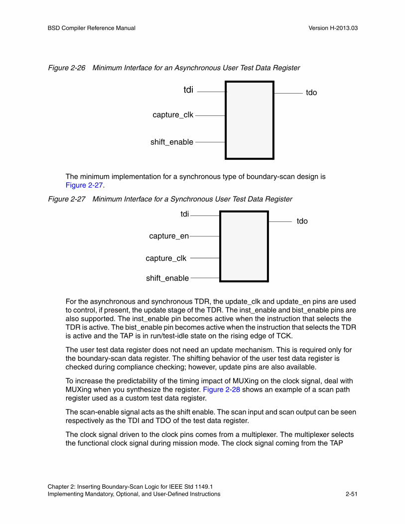
BSD Compiler Reference Manual Version H-2013.03
Figure 2-26 Minimum Interface for an Asynchronous User Test Data Register
The minimum implementation for a synchronous type of boundary-scan design is Figure 2-27.
Figure 2-27 Minimum Interface for a Synchronous User Test Data Register
For the asynchronous and synchronous TDR, the update_clk and update_en pins are used to control, if present, the update stage of the TDR. The inst_enable and bist_enable pins are also supported. The inst_enable pin becomes active when the instruction that selects the TDR is active. The bist_enable pin becomes active when the instruction that selects the TDR is active and the TAP is in run/test-idle state on the rising edge of TCK.
The user test data register does not need an update mechanism. This is required only for the boundary-scan data register. The shifting behavior of the user test data register is checked during compliance checking; however, update pins are also available.
To increase the predictability of the timing impact of MUXing on the clock signal, deal with MUXing when you synthesize the register. Figure 2-28 shows an example of a scan path register used as a custom test data register.
The scan-enable signal acts as the shift enable. The scan input and scan output can be seen respectively as the TDI and TDO of the test data register.
The clock signal driven to the clock pins comes from a multiplexer. The multiplexer selects the functional clock signal during mission mode. The clock signal coming from the TAP
tdi
capture_clk
shift_enable
tdo
tdi
capture_en
shift_enable
tdo
capture_clk
Chapter 2: Inserting Boundary-Scan Logic for IEEE Std 1149.1 Implementing Mandatory, Optional, and User-Defined Instructions 2-51Chapter 2: Inserting Boundary-Scan Logic for IEEE Std 1149.1 Implementing Mandatory, Optional, and User-Defined Instructions 2-51

BSD Compiler Reference Manual H-2013.03BSD Compiler Reference Manual Version H-2013.03
controller is selected during the shift_DR state. You can control the type of selecting logic in the design to meet timing requirements.
Clock signals of BSR or TDR are derived from TCK directly in a synchronous implementation. These signals are derived from TAP in an asynchronous implementation. An asynchronous user test data register is shown in Figure 2-28.
Figure 2-28 Asynchronous User Test Data Register
Connecting the TAP to the User-Defined Test Data RegisterFigure 2-29 shows a representation of the connection between the asynchronous TAP controller and the user-defined test data register. A script for connecting an asynchronous TAP controller to a user-defined test data register is shown in Example 2-8.
shift_enabletdi
capture_clk
inst_enable
tdo
functional clock ~
D D D D D D
Chapter 2: Inserting Boundary-Scan Logic for IEEE Std 1149.1 Implementing Mandatory, Optional, and User-Defined Instructions 2-52

BSD Compiler Reference Manual Version H-2013.03
Figure 2-29 User-Defined Instruction Implemented in an Asynchronous TAP and Test Data Register Style
Example 2-8 Connecting an Asynchronous TAP Controller and a User-Defined Test Data Register
# User-defined test data register (UTDR) and an asynchronous TAP# Polarity default for all signals is active high
set_dft_signal -view spec -type tdi -hookup_pin utdr/tdiset_dft_signal -view spec -type tdo -hookup_pin utdr/tdoset_dft_signal -view spec -type capture_clk -hookup_pin utdr/capture_clkset_dft_signal -view spec -type update_clk -hookup_pin utdr/update_clkset_dft_signal -view spec -type bsd_shift_enable \ -hookup_pin utdr/shift_enable
set_scan_path USER_REG -class bsd -view spec -exact_length 6 \ -hookup [list utdr/tdi \ utdr/capture_clk \ utdr/update_clk \ utdr/shift_enable \
TDI
TCK
tdi
capture_clk
shift_enable
update_clk
tdo
TMS
TRST*
User-defined test data register
DW_TAP_ucController
IRDECODER
IR
Clock_DR
Shift_DR
Update_DR
inst_enable
Functionalserial input
Capture clockinput
Update clockinput
Shift enableinput
1
0
1
0
10
1
0
1
Chapter 2: Inserting Boundary-Scan Logic for IEEE Std 1149.1 Implementing Mandatory, Optional, and User-Defined Instructions 2-53Chapter 2: Inserting Boundary-Scan Logic for IEEE Std 1149.1 Implementing Mandatory, Optional, and User-Defined Instructions 2-53

BSD Compiler Reference Manual H-2013.03BSD Compiler Reference Manual Version H-2013.03
utdr/tdoset_bsd_instruction USER_REG_INST -code “1001” \ -register USER_REG -high utdr/inst_enable
Figure 2-30 shows a representation of the connection between the synchronous TAP controller and the user-defined test data register. A script for connecting a synchronous TAP controller to a user-defined test data register is shown in Example 2-9.
Figure 2-30 User-Defined Instruction Implemented in a Synchronous TAP and Test Data Register Style
Example 2-9 Connecting a Synchronous TAP Controller and a User-Defined Test Data Register
...set_bsd_configuration -style synchronous -ir_width 4...#**************************************************************# User-defined test data register (UTDR) and synchronous TAP# Polarity default for all signals is active high#**************************************************************
set_dft_signal -view spec -type tdi -hookup_pin utdr/tdiset_dft_signal -view spec -type tdo -hookup_pin utdr/tdoset_dft_signal -view spec -type capture_clk -hookup_pin utdr/capture_clkset_dft_signal -view spec -type update_clk -hookup_pin utdr/update_clkset_dft_signal -view spec -type bsd_capture_en \ -hookup_pin utdr/capture_en -active_state 0set_dft_signal -view spec -type bsd_update_en \ -hookup_pin utdr/update_enset_dft_signal -view spec -type bsd_shift_en -hookup_pin utdr/shift_en
tdi tdocapture_clk
shift_enable
User-defined TDR
TAP
sync_capture_en
Shift_DR
TDITCKTMSTRST
IR IR Decoder (user instruction)TDITCKTMSTRST
SysClk TDO
TDO
sync_update_DR
capture_en
update_clk
update_en
inst_enablebist_enable
RunTestState
Chapter 2: Inserting Boundary-Scan Logic for IEEE Std 1149.1 Implementing Mandatory, Optional, and User-Defined Instructions 2-54

BSD Compiler Reference Manual Version H-2013.03
set_dft_signal -view spec -type bist_enable -hookup_pin utdr/bist_en
set_scan_path USER_REG -class bsd -view spec \ -hookup {utdr/tdi \ utdr/capture_clk \ utdr/update_clk \ utdr/capture_en \ utdr/update_en \ utdr/shift_en \ utdr/bist_en \ utdr/tdo}\ -exact_length 45
set_bsd_instruction USER_INST -code “1001” \ -register USER_REG \ -output_condition BSR \ -input_clock_condition TCK \ -high utdr/inst_enable
# NOTE: for a memory BIST controller, use the RUNBIST instruction
MUXing logic is inserted in front of each test data register access pin to select between the functional signal and the TAP controller control signal.
For each user-defined instruction, the decoded signal drives the select pin of the MUXing logic for the corresponding test data register.
If the TDR access pins are initially not connected, BSD Compiler optimization simplifies the MUXing logic to a simple AND gate.
Specifying Output Port ConditioningThe -output_condition option of the set_bsd_instruction command allows you to control how the boundary-scan register controls the output ports when the specified instruction is active. The available values are
• -output_condition BSR
This value puts the boundary-scan register into EXTEST mode when the instruction specified by the set_bsd_instruction command becomes active, regardless of the TAP controller state.
• -output_condition HIGHZ
This value puts the boundary-scan register into HIGHZ mode when the instruction specified by the set_bsd_instruction command becomes active, regardless of the TAP controller state.
Chapter 2: Inserting Boundary-Scan Logic for IEEE Std 1149.1 Implementing Mandatory, Optional, and User-Defined Instructions 2-55Chapter 2: Inserting Boundary-Scan Logic for IEEE Std 1149.1 Implementing Mandatory, Optional, and User-Defined Instructions 2-55
BSD Compiler Reference Manual H-2013.03BSD Compiler Reference Manual Version H-2013.03
• -output_condition NONE
This value keeps the boundary-scan register transparent. This is the default.
You can use the -output_condition option to specify the BSR or HIGHZ output conditions for the INTEST and RUNBIST instructions; a value of NONE is not supported for these instructions. You can specify any of the three output conditions for user-defined instructions. You cannot use this option for the following standard and optional instructions: EXTEST, EXTEST_PULSE, EXTEST_TRAIN, SAMPLE, PRELOAD, BYPASS, HIGHZ, CLAMP, IDCODE, USERCODE.
If you want to condition all your outputs to be in high impedance for the HIGHZ output condition, make sure all output ports are driven by tristate pads.
Specifying Input Clock ConditioningThe -input_clock_condition option of the set_bsd_instruction command allows you to control how the system clocks behave when the specified instruction is active. The available values are
• -input_clock_condition PI
This value does not add any controlling logic to the system clock signals during boundary-scan insertion; each system clock remains driven by the existing connection from its primary input (PI). This is the default.
• -input_clock_condition TCK
This value adds controlling logic to each system clock signal so that it is driven by the test clock TCK when the instruction specified by the set_bsd_instruction command is active and the TAP controller is in the Run-Test-Idle state.
The -input_clock_condition TCK option is normally used to force the system clocks to use TCK when the INTEST or RUNBIST instructions are active, although you can specify it for user-defined instructions as well. You cannot use this option for the following standard and optional instructions: EXTEST, EXTEST_PULSE, EXTEST_TRAIN, SAMPLE, PRELOAD, BYPASS, HIGHZ, CLAMP, IDCODE, USERCODE.
Boundary-scan insertion inserts controlling logic for any primary input signals that it recognizes as clock signals, independent of what timing or test clocks are defined. You can use the preview_dft -bsd cells command to see what primary inputs are identified as clock inputs for boundary-scan insertion:
index port pin(s) package pin function type impl----- ---- ------ ----------- -------- ---- ----7 DIN UDIN/Z - input BC_2 DW_BC_26 TCLK UTCLK/Z - clock BC_4 DW_BC_45 EN UEN/Z - input BC_2 DW_BC_2
Chapter 2: Inserting Boundary-Scan Logic for IEEE Std 1149.1 Implementing Mandatory, Optional, and User-Defined Instructions 2-56

BSD Compiler Reference Manual Version H-2013.03
4 SE USE/Z - input BC_2 DW_BC_23 SI USI/Z - input BC_2 DW_BC_22 SO USO/A - output2 BC_1 DW_BC_11 SYSCLK USYSCLK/Z - clock BC_4 DW_BC_40 DOUT UZ/DOUT - output2 BC_1 DW_BC_1
The controlling logic is inserted inside the boundary-scan register mode control block in accordance with IEEE Std 1149.1 rule number 7.8.2.a. Figure 2-31 shows an example of the controlling logic inserted on a system clock signal for the RUNBIST instruction.
Figure 2-31 Controlling Logic for TCK Input Clock Condition
The behavior of the controlled clock signal is as follows:
• The original system clock is selected when no qualifying instruction is loaded.
• The signal is held inactive when a qualifying instruction is loaded, but the TAP controller is not in the Run-Test-Idle state.
• The TCK clock signal is selected when a qualifying instruction is loaded and the TAP controller is in the Run-Test-Idle state.
If you define a clock port as a linkage port using the set_bsd_linkage_port command, the port is excluded from boundary-scan insertion, and no input condition MUXing logic is added to it.
The -input_clock_condition option does not affect user-defined test data register (UTDR) clock pin connections, even when the UTDR has an existing connection to a system clock. The -input_clock_condition option applies to all other sequential cells clocked by the system clock, but the UTDR clock pin connections are determined by a separate set of rules. For more information on UTDR clock pin connections, see SolvNet article 036718, "How Are User-Defined Test Data Register (UTDR) Connections Made?".
Accessing Internal Scan Through Boundary-Scan LogicDesigners often face restrictions on designs they can put on their ports, so they try to avoid using dedicated ports for internal test. BSD Compiler allows you use boundary-scan logic to control these test signals.
��������������
����������
��
� ����
�
��������������� �������������������� ���� ���� ����
Chapter 2: Inserting Boundary-Scan Logic for IEEE Std 1149.1 Implementing Mandatory, Optional, and User-Defined Instructions 2-57Chapter 2: Inserting Boundary-Scan Logic for IEEE Std 1149.1 Implementing Mandatory, Optional, and User-Defined Instructions 2-57

BSD Compiler Reference Manual H-2013.03BSD Compiler Reference Manual Version H-2013.03
You cannot avoid including boundary-scan ports at the top level, but you can avoid including ports associated with internal scan functionality.
There are three methods for accessing internal scan with boundary-scan logic. You can
• Generate scan-enable signals using boundary-scan logic
• Access internal scan chains between tdi and tdo
• Use scan-through-TAP to daisy chain internal scan to BSR cells
Generating Scan-Enable Signals Using Boundary-Scan LogicIn this configuration you can access the internal scan chains through the top-level ports. These top-level ports can be either dedicated to the scan chain or shared with functional logic.
To generate scan-enable signals on your boundary-scan design,
1. Create a dedicated scan-enable port (scan_en) on your core logic.
2. Specify one instruction with the internal_scan switch.
3. Insert your boundary-scan logic.
4. Run scan insertion using the scan_en port defined on the core as the scan enable.
If boundary-scan insertion is performed earlier in the flow than internal-scan insertion, you should plan to have a dedicated port in the core logic for the scan enable. You should declare this port as the scan_en signal for boundary-scan insertion. You use this port as the scan-enable port for internal scan insertion.
The scan-enable signal generated in the boundary-scan logic is associated with an instruction that makes internal scan active. To generate such a signal and to connect to the correct core logic pin, use the -internal_scan option of the set_bsd_instruction command. The set_bsd_instruction command is discussed in detail in the BSD Compiler User Guide.
The following example shows how the set_bsd_instruction command might be used to generate an internal scan signal:
set_bsd_instruction {chain_1} -code {1001} -internal_scan U_CORE/TEST_SE
This example creates the instruction chain_1, assigns to it the opcode 1001 and associates the instruction with the internal scan port U_CORE/TEST_SE. Because IEEE Std 1149.1 requires a register to be connected between TDI and TDO whenever an instruction is selected, the bypass register is active during this operation.
Chapter 2: Inserting Boundary-Scan Logic for IEEE Std 1149.1 Implementing Mandatory, Optional, and User-Defined Instructions 2-58

BSD Compiler Reference Manual Version H-2013.03
Be aware that a special test protocol file is needed to run ATPG on your design. This protocol file makes sure that the instruction selecting the scan-shift mode is set in the boundary-scan logic before data is shifted.
See the DFT Compiler Scan User Guide for information on inserting internal scan into your core logic.
The advantage to using this method is that parallel access to the scan chains is allowed, reducing test time. It allows you to avoid having a dedicated top-level scan-enable port. The disadvantage is that this implementation does not allow internal scan access through the board-level test mechanism.
Accessing Internal Scan Chains Between TDI and TDOTo achieve complete access of your internal scan through your boundary-scan logic:
Connect all your scan chains between TDI and TDO by following these steps:
1. Declare dedicated input and output ports on your core logic for each scan chain.
2. Identify each scan chain as a user-defined test data register.
3. Specify an instruction that selects each scan chain.
4. Run boundary-scan insertion.
5. Use the dedicated ports as the scan input and scan output of your core logic.
6. Run scan insertion on your core logic.
This method allows you to have complete access to your chips at the board level. You also save a scan-enable port. This method is inconvenient because the scan chains are shifted serially, causing a time-consuming test cycle.
The test protocol for this method is quite large and requires each scan chain to be loaded separately.
Using Scan-Through-TAP to Daisy Chain Internal Scan to BSR CellsThe scan-through-TAP capability in BSD Compiler allows you to daisy chain the scan chains with the BSR chain to become a single chain between TDI and TDO.
To use scan-through-TAP in your flow,
• Specify the scan-through-TAP register.
• Specify the scan-through-TAP instruction.
• Implement scan-through-TAP.
Chapter 2: Inserting Boundary-Scan Logic for IEEE Std 1149.1 Implementing Mandatory, Optional, and User-Defined Instructions 2-59Chapter 2: Inserting Boundary-Scan Logic for IEEE Std 1149.1 Implementing Mandatory, Optional, and User-Defined Instructions 2-59

BSD Compiler Reference Manual H-2013.03BSD Compiler Reference Manual Version H-2013.03
This method allows you to automate the process of
• Specifying the scan-through-TAP register containing multiple scan-chains and boundary-scan registers
• Daisy-chaining the specified scan chains or the BSRs in the scan-through-TAP register
• Synthesizing the circuitry to control the scan-chain operation by IEEE Std. 1149.1 instruction
Generating Mode Signals for the BSR Cells
During insert_dft, the logic required to generate the mode signal for each BSR and the instruction decoding logic for HIGHZ, CLAMP, and user-defined instructions are inserted by using unmapped generic components.
The design is put under the design name
name_of_top_level_design_BSR_mode_inst_design
This block is instantiated in the BSR block. Its instance name is
name_of_top_level_design_BSR_mode_inst
The BSR cells and mode generation block created by insert_dft are shown in Figure 2-32.
Figure 2-32 BSR Cells and Mode Logic at MyTop_BSR_top_design Level
BSR cell:
Mode logicgeneration block
tdi
tdo
MyTop_in2_bsr4
BSR cell:
MyTop_out1_bsr4
BSR cell:
MyTop_in1_bsr4
BSR cell:
MyTop_out2_bsr1
tap_statesignals
MyTop_BSR_mode_inst
Chapter 2: Inserting Boundary-Scan Logic for IEEE Std 1149.1 Generating Mode Signals for the BSR Cells 2-60

BSD Compiler Reference Manual Version H-2013.03
After insert_dft your boundary scan is present in your design in an unmapped state. The next step is to synthesize the logic.
The generic boundary-scan logic generated by insert_dft is shown in Figure 2-33.
Figure 2-33 Boundary-Scan Logic at the Top Level
Previewing Your Boundary-Scan Design
You can preview the results of boundary-scan insertion by using the preview_dft command.
The preview_dft command invokes the boundary-scan architect embedded in BSD Compiler. The boundary-scan architect provides you with a map of the boundary-scan implementation.
The preview_dft command validates all pad design instances against the specified pad type and the access list. By default, all pad design instances are validated unless otherwise specified with the set_bsd_configuration -check_pad_designs.
DWTAP
MyTop_BSR_top_inst
Core Logic
Chapter 2: Inserting Boundary-Scan Logic for IEEE Std 1149.1 Previewing Your Boundary-Scan Design 2-61Chapter 2: Inserting Boundary-Scan Logic for IEEE Std 1149.1 Previewing Your Boundary-Scan Design 2-61

BSD Compiler Reference Manual H-2013.03BSD Compiler Reference Manual Version H-2013.03
When you use the preview_dft command before you use insert_dft, the boundary-scan architect tells you how the boundary-scan logic is to be implemented. For more information about using the preview_dft command, see the BSD Compiler User Guide.
Optimization Techniques
After inserting the boundary-scan logic, you can use three cell-level optimization techniques to minimize the inserted logic’s impact on the area and timing of your design.
Merging Boundary-Scan Register CellsBefore performing any cell-merging operations, preview the results of boundary-scan insertion by using the preview_dft command.
The insert_dft command performs complete boundary-scan insertion, providing a boundary-scan register cell for each port and control signal. Your design might have feed-through connections or tristate output drivers directly fed by an input driver. In such cases, the BSR cells on the feed-through connections or on the output drivers are not necessary. The insert_dft command automatically merges cells in two specific situations:
• The parallel output of an input BSR cell drives the parallel input of an output BSR cell.
In this case the input BSR cell is removed, leaving a direct connection from the input pad-cell output to the parallel input of the output BSR cell.
• The parallel output of an input BSR cell drives the parallel input of a control BSR cell.
BSD Compiler operates the same kind of BSR cell merging as described in the previous case.
Chapter 2: Inserting Boundary-Scan Logic for IEEE Std 1149.1 Optimization Techniques 2-62
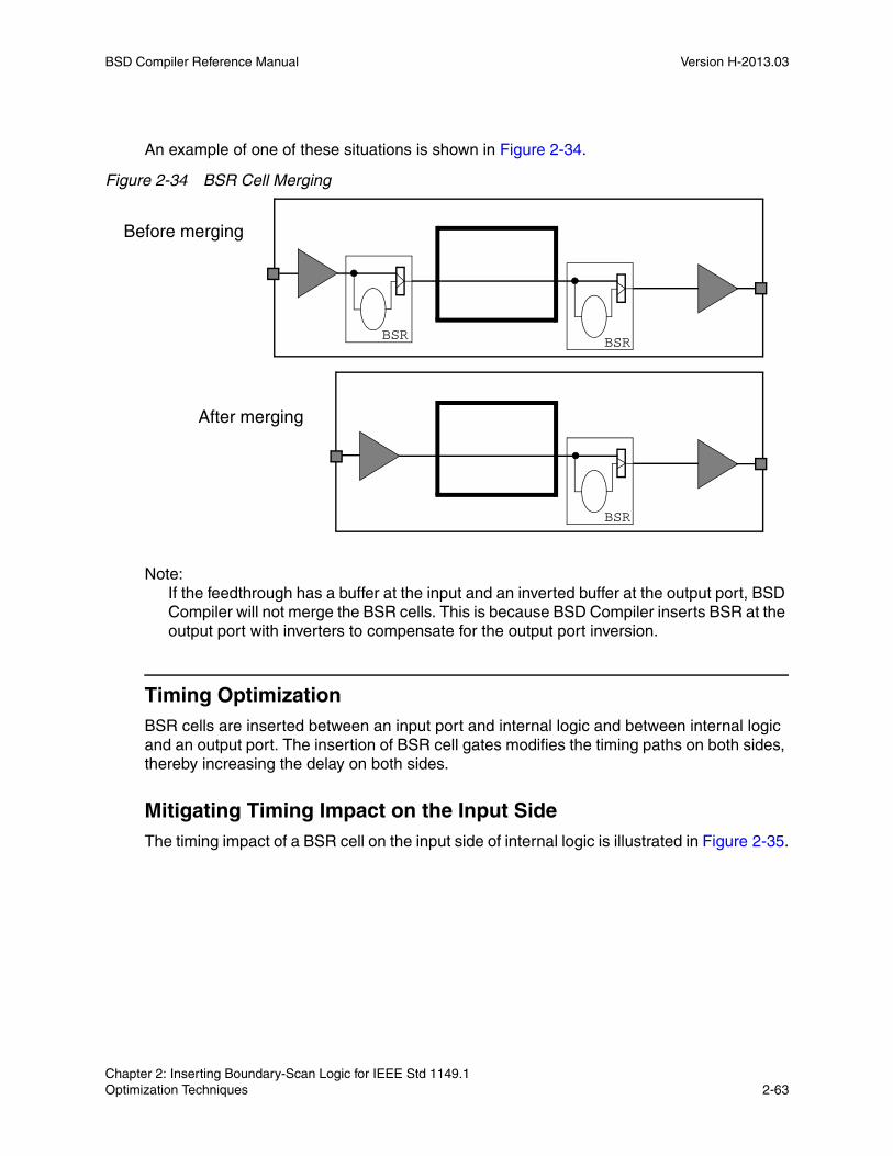
BSD Compiler Reference Manual Version H-2013.03
An example of one of these situations is shown in Figure 2-34.
Figure 2-34 BSR Cell Merging
Note: If the feedthrough has a buffer at the input and an inverted buffer at the output port, BSD Compiler will not merge the BSR cells. This is because BSD Compiler inserts BSR at the output port with inverters to compensate for the output port inversion.
Timing OptimizationBSR cells are inserted between an input port and internal logic and between internal logic and an output port. The insertion of BSR cell gates modifies the timing paths on both sides, thereby increasing the delay on both sides.
Mitigating Timing Impact on the Input SideThe timing impact of a BSR cell on the input side of internal logic is illustrated in Figure 2-35.
BSRBSR
BSR
Before merging
After merging
Chapter 2: Inserting Boundary-Scan Logic for IEEE Std 1149.1 Optimization Techniques 2-63Chapter 2: Inserting Boundary-Scan Logic for IEEE Std 1149.1 Optimization Techniques 2-63

BSD Compiler Reference Manual H-2013.03BSD Compiler Reference Manual Version H-2013.03
Figure 2-35 Timing Impact on Input
You can mitigate the timing impact by substituting a control-and-observe cell with a control-only cell, or you can eliminate the cell altogether.
If the timing path is critical, you can remove the default control-and-observe BSR cell (BC_1, BC_2) and substitute an observe-only BSR cell (BC_4) where no multiplexing logic is inserted in the functional path. IEEE Std 1149.1 allows input observe-only BSR cells if the INTEST instruction is not implemented in the design.
If you can afford to, you might want to remove the BSR cell from the input if it is on a timing-critical path. Although this action violates IEEE Std 1149.1, BSD Compiler considers it to be a tolerable violation. Its main impact is to reduce the design’s testability.
Mitigating Timing Impact on the Output SideThe timing impact on the output side of the internal logic is illustrated in Figure 2-36.
0.3 ns
0.3 ns + 0.5 ns
BSR
Before Boundary-Scan Insertion
After Boundary-Scan Insertion
Core logic
Core logic
Chapter 2: Inserting Boundary-Scan Logic for IEEE Std 1149.1 Optimization Techniques 2-64

BSD Compiler Reference Manual Version H-2013.03
Figure 2-36 Timing Impact on Output
The only alternative is to remove the BSR cell if it is on a timing-critical path. This action violates IEEE Std 1149.1, but BSD Compiler considers it to be a tolerable violation, reducing the design’s testability.
Specifying Timing ConstraintsYou can specify timing constraints on ports by using the set_max_delay command.
set_max_delay -from in00 -to U1/D 2.9set_max_delay -from U86/Z -to out00 2.3
For more information on how to constrain the timing in your design, see the Design Compiler documentation.
Area Optimization By default insert_dft adds a control BSR cell for each output tristate driver enable pin. The area overhead caused by this insertion can be significant. Consequently, you might want to share a control BSR cell among several enable signals. This reduces the number of BSR cells and the total area consumed by the BSR.
The board-level test vector software activates one tristate output at a time, reducing the noise generated by the transition. To avoid ground bounce problems, limit the number of
0.3 ns
0.3 ns + 0.5 ns
BSR
Before Boundary-Scan Insertion
After Boundary-Scan Insertion
Core logic
Core logic
Chapter 2: Inserting Boundary-Scan Logic for IEEE Std 1149.1 Optimization Techniques 2-65Chapter 2: Inserting Boundary-Scan Logic for IEEE Std 1149.1 Optimization Techniques 2-65

BSD Compiler Reference Manual H-2013.03BSD Compiler Reference Manual Version H-2013.03
enable pins driven by a single BSR cell. You can limit the number of enable pins one control BSR can drive by using the set_bsd_configuration -control_cell_max_fanout.
Figure 2-37 shows an example of area-driven boundary-scan optimization.
Figure 2-37 Area-Driven Boundary-Scan Optimization
c_1
Before After
c_2
c_3
c_4
c_5
c_6
c_7
c_8
c_9
c_10
c_11
c_12
c_1
c_2
c_6
c_7
c_8
c_9
c_10
c_12
c_4
Chapter 2: Inserting Boundary-Scan Logic for IEEE Std 1149.1 Optimization Techniques 2-66
3Inserting Boundary-Scan Logic for IEEE Std 1149.6 3
This chapter describes how to insert boundary-scan logic for IEEE Std 1149.6-2003 into your design and preview the results before compliance checking. Various sections describe boundary-scan requirements, initializing and inserting the TAP controller, and implementing instructions.
This chapter includes the following sections:
• IEEE Std 1149.6 Overview
• Boundary-Scan Components for IEEE Std 1149.6
• The EXTEST_TRAIN Instruction
• The EXTEST_PULSE Instruction
3-1

BSD Compiler Reference Manual H-2013.03BSD Compiler Reference Manual Version H-2013.03
IEEE Std 1149.6 Overview
This section provides an overview of IEEE Std 1149.6 logic. BSD Compiler synthesizes the IEEE Std 1149.6 in conjunction with the IEEE Std 1149.1, and generates a IEEE Std 1149.6 compliant BSDL file, and the IEEE Std 1149.6 patterns for verification.
The compliance checker validates the IEEE Std 1149.1 for designs with IEEE Std 1149.6 logic, and the validation of the IEEE Std 1149.6 patterns is done by BSD patterns simulation. There is no support for AC_8, AC_9, and AC_10 BSR cells.
For more information on IEEE Standard 1149.6, see the BSD Compiler User Guide.
Boundary-Scan Components for IEEE Std 1149.6
This standard defines new BSR AC selection cells and new BSR data cells on AC pins that have drive capability. Figure 3-1 shows the IEEE Std 1149.1 original cell type with AC_1 and AC_2 cells and the changes made to it required by IEEE Std 1149.6.
Chapter 3: Inserting Boundary-Scan Logic for IEEE Std 1149.6 IEEE Std 1149.6 Overview 3-2
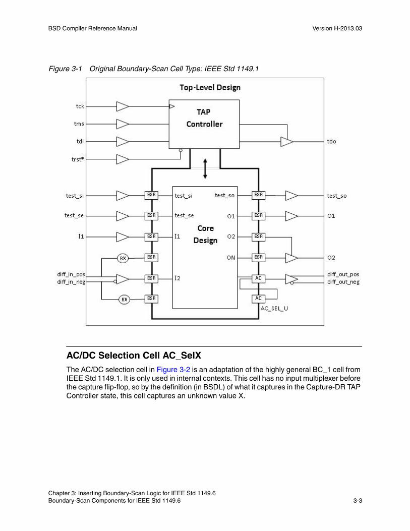
BSD Compiler Reference Manual Version H-2013.03
Figure 3-1 Original Boundary-Scan Cell Type: IEEE Std 1149.1
AC/DC Selection Cell AC_SelX The AC/DC selection cell in Figure 3-2 is an adaptation of the highly general BC_1 cell from IEEE Std 1149.1. It is only used in internal contexts. This cell has no input multiplexer before the capture flip-flop, so by the definition (in BSDL) of what it captures in the Capture-DR TAP Controller state, this cell captures an unknown value X.
Chapter 3: Inserting Boundary-Scan Logic for IEEE Std 1149.6 Boundary-Scan Components for IEEE Std 1149.6 3-3Chapter 3: Inserting Boundary-Scan Logic for IEEE Std 1149.6 Boundary-Scan Components for IEEE Std 1149.6 3-3
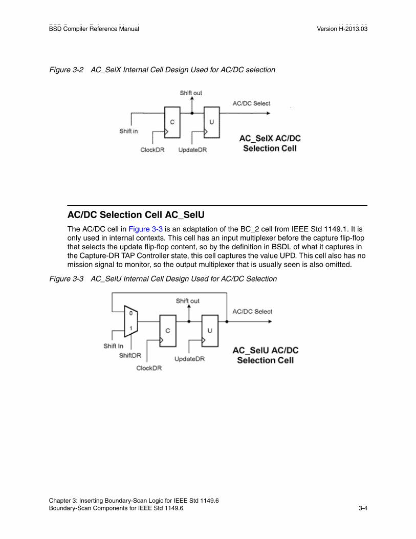
BSD Compiler Reference Manual H-2013.03BSD Compiler Reference Manual Version H-2013.03
Figure 3-2 AC_SelX Internal Cell Design Used for AC/DC selection
AC/DC Selection Cell AC_SelU The AC/DC cell in Figure 3-3 is an adaptation of the BC_2 cell from IEEE Std 1149.1. It is only used in internal contexts. This cell has an input multiplexer before the capture flip-flop that selects the update flip-flop content, so by the definition in BSDL of what it captures in the Capture-DR TAP Controller state, this cell captures the value UPD. This cell also has no mission signal to monitor, so the output multiplexer that is usually seen is also omitted.
Figure 3-3 AC_SelU Internal Cell Design Used for AC/DC Selection
Chapter 3: Inserting Boundary-Scan Logic for IEEE Std 1149.6 Boundary-Scan Components for IEEE Std 1149.6 3-4

BSD Compiler Reference Manual Version H-2013.03
Output Data Cell AC_1 (Supports INTEST) The AC_1 cell in Figure 3-4 is an adaptation of the general BC_1 cell from IEEE Std 1149.1. This cell supports the INTEST instruction. Note that the BC_1 cell can be used in contexts other than supplying data to output drivers (input cells, control cells), but the AC_1 cell supports only the Output2 and Output3 contexts.
Figure 3-4 AC_1 Output Data Cell Adapted From BC_1
The circuitry added for support of AC EXTEST test instructions is circled in the figure.
Output Data Cell AC_2 The AC_2 cell in Figure 3-5 is an adaptation of the BC_2 cell from IEEE Std 1149.1. Note that the BC_2 cell can be used in contexts other than supplying data to output drivers (input cells, control cells), but that the AC_2 cell supports only the Output2 and Output3 contexts. This cell does not support INTEST. The circuitry added for support of AC EXTEST test instructions is circled in the figure.
Chapter 3: Inserting Boundary-Scan Logic for IEEE Std 1149.6 Boundary-Scan Components for IEEE Std 1149.6 3-5Chapter 3: Inserting Boundary-Scan Logic for IEEE Std 1149.6 Boundary-Scan Components for IEEE Std 1149.6 3-5

BSD Compiler Reference Manual H-2013.03BSD Compiler Reference Manual Version H-2013.03
Figure 3-5 AC_2 Output Data Cell Adapted From BC_2
BIDI Output Cell AC_7 (Supports INTEST) The AC_7 cell in Figure 3-6 (shown with its companion BC_2 control cell) is an adaptation of the bidirectional BC_7 cell from IEEE Std 1149. This cell supports the INTEST instruction. The circuitry added for support of AC EXTEST test instructions is circled.
Chapter 3: Inserting Boundary-Scan Logic for IEEE Std 1149.6 Boundary-Scan Components for IEEE Std 1149.6 3-6

BSD Compiler Reference Manual Version H-2013.03
Figure 3-6 AC_7 Output Cell Adapted From BC_7
AC Cell Mode Controls Table 3-1 defines the mode signal generation for the AC output cells.
Table 3-1 AC Output Mode Generation
Instruction Mode 1 Mode 2 Mode 3 Mode 4 Mode 5
EXTEST 1 0 1 1 1
PRELOAD 0 0 1 X 0
SAMPLE 0 0 1 0 0
Chapter 3: Inserting Boundary-Scan Logic for IEEE Std 1149.6 Boundary-Scan Components for IEEE Std 1149.6 3-7Chapter 3: Inserting Boundary-Scan Logic for IEEE Std 1149.6 Boundary-Scan Components for IEEE Std 1149.6 3-7

BSD Compiler Reference Manual H-2013.03BSD Compiler Reference Manual Version H-2013.03
Note: The EXTEST entry includes EXTEST, EXTEST_PULSE, and EXTEST_TRAIN.
The row for the INTEST instruction for cells AC_2, AC_8, and AC_10 that do not support INTEST should be ignored.
General AC Pin Driver StructureA possible implementation for a pin driver that supports IEEE Std 1149.1 instructions as well as AC test capabilities provided by IEEE Std 1149.6 is shown in Figure 3-7. This implementation is a simple adaptation of a commonly used Boundary-Scan Register cell design (BC_1), where an extra multiplexer, controlled by AC Mode is used to select either the update register content, or that same content modulated by an exclusive-OR gate with the AC test signal.
INTEST 0 1 0 0 1
RUNBIST X X 0 X 1
CLAMP 1 X 1 X 1
HIGHZ X X 0 X X
Table 3-1 AC Output Mode Generation (Continued)
Instruction Mode 1 Mode 2 Mode 3 Mode 4 Mode 5
Chapter 3: Inserting Boundary-Scan Logic for IEEE Std 1149.6 Boundary-Scan Components for IEEE Std 1149.6 3-8

BSD Compiler Reference Manual Version H-2013.03
Figure 3-7 General AC Pin Driver Structure
Test Receiver With BSR CellsIn Figure 3-8, the retiming latch ensures that the gating signal always encloses the TCK='1' pulse that is intended to gate. TMS='1' in the equation ensures that the hysteretic memory initializes only on transitions from one of the Exit*_DR states to Update_DR, and not to PauseDR or to ShiftDR. The timing diagrams help in understanding the circuit.
Chapter 3: Inserting Boundary-Scan Logic for IEEE Std 1149.6 Boundary-Scan Components for IEEE Std 1149.6 3-9Chapter 3: Inserting Boundary-Scan Logic for IEEE Std 1149.6 Boundary-Scan Components for IEEE Std 1149.6 3-9
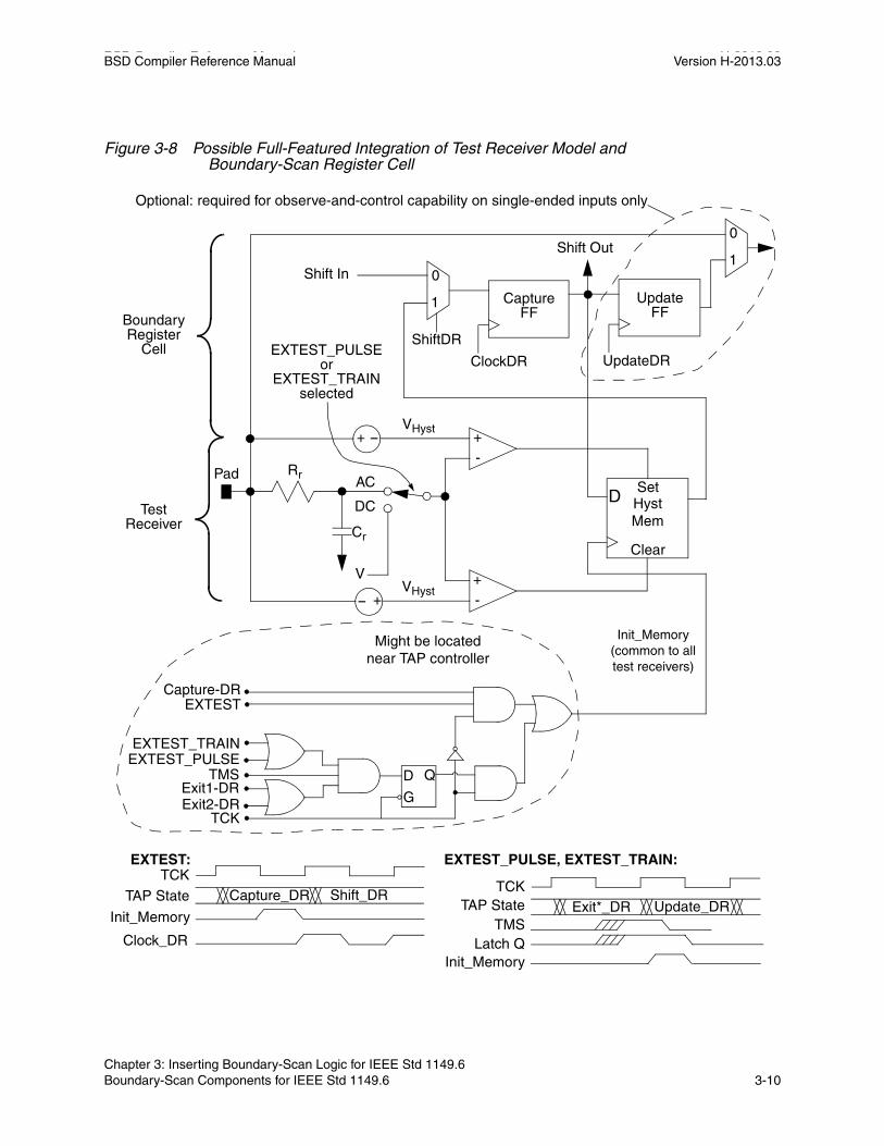
BSD Compiler Reference Manual H-2013.03BSD Compiler Reference Manual Version H-2013.03
Figure 3-8 Possible Full-Featured Integration of Test Receiver Model and Boundary-Scan Register Cell
Capture FF
Update FFBoundary
Register Cell
Test Receiver
1
0Shift Out
UpdateDRClockDR
1
0
ShiftDR
Shift In
D
+-
+
+-+
PadAC
DC
V
Cr
EXTEST_PULSE, EXTEST_TRAIN:
EXTEST_PULSEor
EXTEST_TRAIN selected
VHyst
VHyst
RrSet
Clear
HystMem
Optional: required for observe-and-control capability on single-ended inputs only
-
-
Capture_DR Shift_DRTAP State
Init_Memory
Clock_DR
TCKEXTEST:
Exit*_DR Update_DRTAP StateTMS
Latch QInit_Memory
TCK
Init_Memory(common to alltest receivers)
TMS
EXTEST
TCK
EXTEST_TRAINEXTEST_PULSE
Capture-DR
Exit2-DRExit1-DR
D
G
Q
Might be located near TAP controller
Chapter 3: Inserting Boundary-Scan Logic for IEEE Std 1149.6 Boundary-Scan Components for IEEE Std 1149.6 3-10

BSD Compiler Reference Manual Version H-2013.03
Note: The generated clock, init_memory, is suitable for rising edge-sensitive behavior only.
In Figure 3-9, the circuit provides a negative-active level-sensitive clock signal. A retiming latch and TMS are used to ensure the correct transitions are taking place.
For a level-sensitive clock, the trailing edge of the clock pulse needs to be the active edge, that is, placed at the TCK edge as required by the IEEE Std 1149.6. In order to place it correctly, ensure that a transition is taking place from Select_DR_Scan to Capture_DR.
The circuit creates a level-sensitive clock with the trailing edge as the active edge. By making it negative-active, the trailing edge is also the rising edge, so the clock produced by this circuit can be used with test receivers (RX) exhibiting either level-sensitive or edge-sensitive behavior or even a mix of behaviors. Due to this flexibility, the circuit shown in Figure 3-9 might be preferred over that in Figure 3-8 for implementation when the type of test receivers being supported cannot be determined in advance.
Chapter 3: Inserting Boundary-Scan Logic for IEEE Std 1149.6 Boundary-Scan Components for IEEE Std 1149.6 3-11Chapter 3: Inserting Boundary-Scan Logic for IEEE Std 1149.6 Boundary-Scan Components for IEEE Std 1149.6 3-11
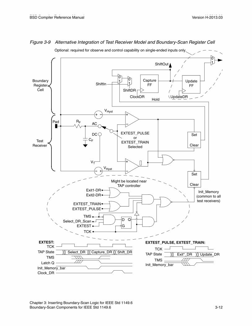
BSD Compiler Reference Manual H-2013.03BSD Compiler Reference Manual Version H-2013.03
Figure 3-9 Alternative Integration of Test Receiver Model and Boundary-Scan Register Cell
TMS
EXTEST
TCK
EXTEST_TRAINEXTEST_PULSE
Exit1-DRExit2-DR
Select_DR_Scan D
G
Q
+
-
+
-
CaptureFF
UpdateFF
Set
Clear
Set
Clear
VHyst
VHyst
VT
CF
AC
DC
RFPad
+
+
-
-
ClockDR UpdateDR
EXTEST_PULSEor
EXTEST_TRAINSelected
01
01
01ShiftIn
ShiftDR
Hold
ShiftOut
Init_Memory(common to alltest receivers)
BoundaryRegister
Cell
TestReceiver
Might be located near TAP controller
Optional: required for observe and control capability on single-ended inputs only
Select_DR Capture_DR Shift_DRExit*_DR Update_DR
TAP State
TMS
Latch QInit_Memory_barClock_DR
TCKEXTEST:
TCKTAP State
TMSInit_Memory_bar
EXTEST_PULSE, EXTEST_TRAIN:
Chapter 3: Inserting Boundary-Scan Logic for IEEE Std 1149.6 Boundary-Scan Components for IEEE Std 1149.6 3-12
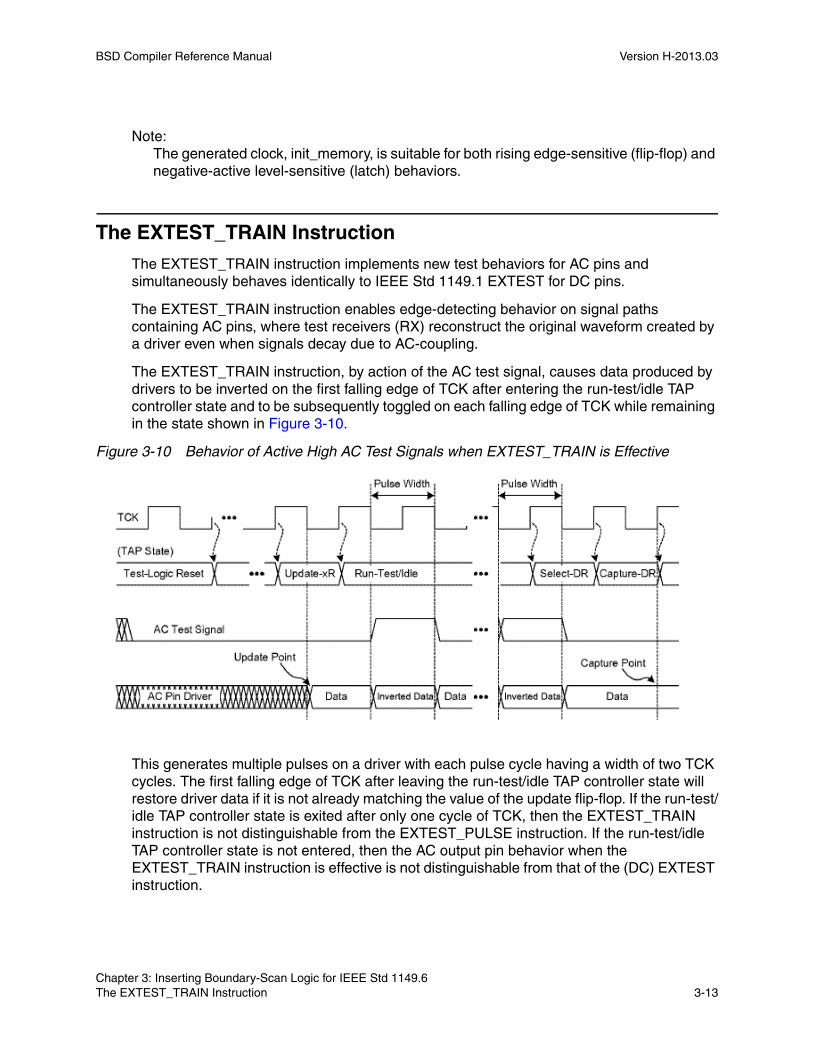
BSD Compiler Reference Manual Version H-2013.03
Note: The generated clock, init_memory, is suitable for both rising edge-sensitive (flip-flop) and negative-active level-sensitive (latch) behaviors.
The EXTEST_TRAIN Instruction
The EXTEST_TRAIN instruction implements new test behaviors for AC pins and simultaneously behaves identically to IEEE Std 1149.1 EXTEST for DC pins.
The EXTEST_TRAIN instruction enables edge-detecting behavior on signal paths containing AC pins, where test receivers (RX) reconstruct the original waveform created by a driver even when signals decay due to AC-coupling.
The EXTEST_TRAIN instruction, by action of the AC test signal, causes data produced by drivers to be inverted on the first falling edge of TCK after entering the run-test/idle TAP controller state and to be subsequently toggled on each falling edge of TCK while remaining in the state shown in Figure 3-10.
Figure 3-10 Behavior of Active High AC Test Signals when EXTEST_TRAIN is Effective
This generates multiple pulses on a driver with each pulse cycle having a width of two TCK cycles. The first falling edge of TCK after leaving the run-test/idle TAP controller state will restore driver data if it is not already matching the value of the update flip-flop. If the run-test/idle TAP controller state is exited after only one cycle of TCK, then the EXTEST_TRAIN instruction is not distinguishable from the EXTEST_PULSE instruction. If the run-test/idle TAP controller state is not entered, then the AC output pin behavior when the EXTEST_TRAIN instruction is effective is not distinguishable from that of the (DC) EXTEST instruction.
Chapter 3: Inserting Boundary-Scan Logic for IEEE Std 1149.6 The EXTEST_TRAIN Instruction 3-13Chapter 3: Inserting Boundary-Scan Logic for IEEE Std 1149.6 The EXTEST_TRAIN Instruction 3-13
BSD Compiler Reference Manual H-2013.03BSD Compiler Reference Manual Version H-2013.03
The derivation of the output signal inversions from the falling edge of TCK when a pulse train is generated guarantees that the duty cycle of TCK does not affect the squareness of the pulse train. However, interruptions in TCK that are allowed by IEEE Std 1149.1 will have the effect of stretching a pulse or duration between pulses. Typical TCK frequencies used in test equipment might vary from hundreds of kilohertz to tens of megahertz. The TCK rate used to drive a chain of devices is also limited by the slowest TCK rate of any member of that chain, as documented in BSDL. This standard is intended for use in many device types, including devices where system clock rates are several decades higher than these typical TCK rates. The device designer needs to remember this basic range on TCK rates and how it might be quite different from the mission performance range.
As a device designer, you might have some flexibility in driver implementation if the driver has dynamic behavior that must be conditioned by some minimum number of pulses before a downstream receiver actually samples its output. Rules specified in the IEEE Std 1149.6 allow you to further state a time frame within which these pulses should occur. However, this begins to approximate a minimum TCK requirement that should be observed by testing tools, which might prevent a given tool from being able to perform the EXTEST_TRAIN instruction. The IEEE Std 1149.6 recommends designers not add this restriction whenever possible, so as to avoid implementing an instruction that cannot be used practically. It also recommends using a large maximum time period when such time is needed.
The EXTEST_PULSE Instruction
The EXTEST_PULSE instruction implements new test behaviors for AC pins and simultaneously behaves identically to IEEE Std 1149.1 EXTEST for DC pins.
The EXTEST_PULSE instruction enables edge-detecting behavior on signal paths containing AC pins, where test receivers (RX) reconstruct the original waveform created by a driver even when signals decay due to AC-coupling.
One possible mechanism for achieving the required behavior is with an internal signal called the AC test signal. The AC test signal will be made exclusive-OR with the signal from the associated Boundary-Scan Register data cell, and it causes data produced by drivers to be inverted on the first falling edge of TCK after entering the run-test/idle TAP controller state and to be restored on the first falling edge of TCK after leaving this state, as shown in Figure 3-11. This generates a pulse of inverted data on a driver that is as wide as the time spent in the run-test/idle TAP controller state. If the run-test/idle TAP controller state is not entered, then the output behavior of the AC pins is not distinguishable from that of the DC EXTEST instruction.
Chapter 3: Inserting Boundary-Scan Logic for IEEE Std 1149.6 The EXTEST_PULSE Instruction 3-14

BSD Compiler Reference Manual Version H-2013.03
Figure 3-11 Behavior of Active High AC Test Signals when EXTEST_PULSE is Effective
The device designer might specify a minimum width requirement for pulses produced by the EXTEST_PULSE instruction that exceeds the minimum width necessitated by rules provided by this standard. This allows you to specify a minimum pulse width produced by the EXTEST_PULSE instruction that is longer than the minimum already governed by the rules for determining T-test. A minimum pulse width allows critical time constants for AC-coupling or edge detection to decay to a static DC level. You might have other design parameters that require more time than this minimum.
Note: For more information on the IEEE Std 1149.6, contact the IEEE Society.
Chapter 3: Inserting Boundary-Scan Logic for IEEE Std 1149.6 The EXTEST_PULSE Instruction 3-15Chapter 3: Inserting Boundary-Scan Logic for IEEE Std 1149.6 The EXTEST_PULSE Instruction 3-15

BSD Compiler Reference Manual H-2013.03BSD Compiler Reference Manual Version H-2013.03
Chapter 3: Inserting Boundary-Scan Logic for IEEE Std 1149.6 The EXTEST_PULSE Instruction 3-16

4Checking IEEE Std 1149.1 Compliance 4
This chapter describes how to check compliance of your completed boundary-scan design against IEEE Standard 1149.1 to ensure that it behaves correctly and can be used by any board-level tester that complies with IEEE Standard 1149.1.
BSD Compiler provides complete compliance checking through the check_bsd command. The check_bsd command verifies your boundary-scan design against the IEEE Std 1149.1 rules. The check_bsd command is an easy and fast way to verify your boundary-scan design without generating a testbench or running an exhaustive functional simulation.
This chapter includes the following sections:
• Introduction
• Phase One: Extracting and Verifying the TAP Controller
• Phase Two: Extracting the Shift Register Stages of IEEE Std 1149.1 Registers
• Phase Three: Extracting Implemented Instructions and Test Data Registers
• Phase Four: Inferring BSR Cell Characteristics
4-1

BSD Compiler Reference Manual H-2013.03BSD Compiler Reference Manual Version H-2013.03
Introduction
The check_bsd command performs compliance checking and design verification, and it generates messages to inform you about possible problems with the design. Whether you generate your boundary-scan design with BSD Compiler or with another tool, check_bsd is valuable. Often designs pass through many hands, resulting in potential errors. The check_bsd command uses symbolic simulation to discover problems in the boundary-scan design.
BSD Compiler implements the check_bsd command in three different ways:
• As a standalone command
The check_bsd command is generally run as an individual command. When you run check_bsd, you can obtain information about your boundary-scan design then debug violations to the IEEE Std 1149.1. This chapter discusses the use of check_bsd in this manner.
• Within the write_bsdl command, as a BSDL preprocessor
The write_bsdl command automatically executes check_bsd if no previous run of check_bsd was done or if the results of the previous run are invalid.
• Within the create_bsd_patterns command, as a boundary-scan test-vector preprocessor
The create_bsd_patterns command automatically executes check_bsd if no previous run of check_bsd was done or if the results of the previous run are invalid.
check_bsd MessagesWhile analyzing your boundary-scan design check_bsd provides you with feedback by using messages numbered TEST-801, TEST-802, and so on.
The messages generated by check_bsd can have one of three levels of severity:
1. Information
Information messages provide you with information about the status of the compliance-checking process or more details about a specific violation. This is the lowest level of severity.
2. Warning
Warning messages indicate a boundary-scan violation. A warning message means your design doesn’t fully comply with IEEE Std 1149.1 and this might affect the test procedure at the board level.
Chapter 4: Checking IEEE Std 1149.1 Compliance Introduction 4-2

BSD Compiler Reference Manual Version H-2013.03
If check_bsd produces warning messages for your design, you should fix the problem to achieve a verified and compliant design. This is the intermediate level of severity.
3. Error
Error Messages indicate the existence of a boundary-scan violation that is so severe that check_bsd cannot proceed. After an error is reported, check_bsd stops processing your design. No BSDL or patterns are generated.
You can downgrade certain error messages to a warning status with the set_message_severity command. This command is described in the BSD Compiler User Guide.
If check_bsd produces error messages for your design, you must fix them to achieve a verified and compliant design.
This is the highest level of severity. You must fix error violations to continue checking your design.
Reporting Multiple ViolationsWhen a violation occurs one time, it might be present in other areas of the design as well. As a consequence, two information messages exist to identify the number of times a violation has occurred.
• If a violation occurs only one time more, the information message TEST-801 is generated. For example,
Information: There is 1 such other violation. (TEST-801)
The TEST-801 message immediately follows the violation message to which it refers. It is generated in both the verbose and the nonverbose modes of check_bsd. In the verbose mode of check_bsd, the name of the object containing the same violation is listed. To address the problems that cause the TEST-801 message to be generated, investigate and fix the causes of the previous message and run check_bsd again.
• If a violation occurs more than one more time, the information message TEST-802 is generated. For example,
Information: There are 8 such other violations. (TEST-802)
The TEST-802 message immediately follows the violation message to which it refers. It is generated in both the verbose and the nonverbose modes of check_bsd. In the verbose mode of check_bsd, the name of the objects containing the same violation are listed. To address the problems that cause the TEST-802 message to be generated, investigate and fix the causes of the previous message and run check_bsd again.
Chapter 4: Checking IEEE Std 1149.1 Compliance Introduction 4-3Chapter 4: Checking IEEE Std 1149.1 Compliance Introduction 4-3
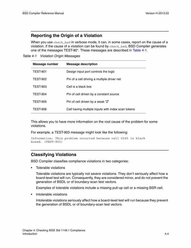
BSD Compiler Reference Manual H-2013.03BSD Compiler Reference Manual Version H-2013.03
Reporting the Origin of a ViolationWhen you use check_bsd in verbose mode, it can, in some cases, report on the cause of a violation. If the cause of a violation can be found by check_bsd, BSD Compiler generates one of the messages TEST-90*. These messages are described in Table 4-1.
This allows you to have more information on the root cause of the problem for some violations.
For example, a TEST-903 message might look like the following:
Information: This problem occurred because cell U245 is black boxed. (TEST-903)
Classifying ViolationsBSD Compiler classifies compliance violations in two categories:
• Tolerable violations
Tolerable violations are typically not severe violations. They don’t seriously affect how a board-level test will run. Consequently, they are considered minor, and do not prevent the generation of BSDL or of boundary-scan test vectors.
Examples of tolerable violations include a missing pull-up cell or a missing BSR cell.
• Intolerable violations
Intolerable violations seriously affect how a board-level test will run because they prevent the generation of BSDL or of boundary-scan test vectors.
Table 4-1 Violation Origin Messages
Message number Message description
TEST-901 Design input port controls the logic
TEST-902 Pin of a cell driving a multiple driver net
TEST-903 Cell is a black box
TEST-904 Pin of cell driven by a constant source
TEST-905 Pin of cell driven by a weak “Z”
TEST-906 Cell having multiple inputs with index scan tokens
Chapter 4: Checking IEEE Std 1149.1 Compliance Introduction 4-4

BSD Compiler Reference Manual Version H-2013.03
Examples of intolerable violations include a missing bypass register or a noncompliant boundary-scan register.
Note: Some intolerable violations can be down graded from status error to warning. Refer to the BSD Compiler User Guide for details.
Preparing to Use check_bsdBefore you begin checking your design for compliance with IEEE Std 1149.1, confirm the following items:
• Your netlist and the logic libraries to which it is mapped are all in the Design Compiler database.
If you have not loaded your netlist and the logic libraries to which it is mapped into the Design Compiler database, you must do so by using Design Compiler commands.
• Your netlist contains IEEE Std 1149.1 logic.
• All pads used in the design have a valid function in the logic library.
❍ Run link to identify unresolved references and fix.
❍ Run check_design to check for other multiple driven nets.
❍ Run report_cell and report_reference to identify black boxes.
❍ Run report_hierarchy to show the hierarchy references.
❍ Run check_bsd -infer_instructions false to have check_bsd look for implement instructions information passed by insert_bsd. If not found, check_bsd looks for explicit set_bsd_instruction specifications you provided. If neither exist, check_bsd proceeds as it would if you set this option to true. Setting this option to true causes BSD Compiler to extract the instructions automatically.
• All TAP ports are defined.
• All compliance-enable ports are defined.
Figure 4-1 shows Design Compiler tips for checking your design before compliance checking.
Chapter 4: Checking IEEE Std 1149.1 Compliance Introduction 4-5Chapter 4: Checking IEEE Std 1149.1 Compliance Introduction 4-5
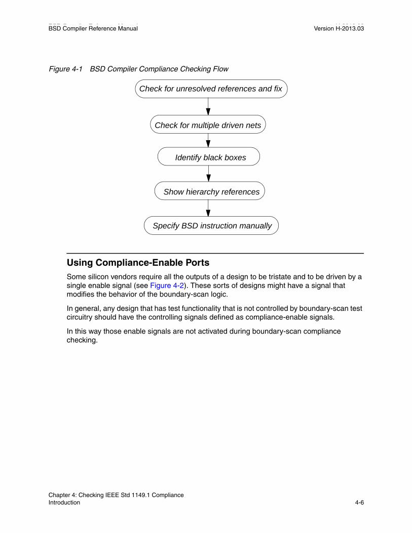
BSD Compiler Reference Manual H-2013.03BSD Compiler Reference Manual Version H-2013.03
Figure 4-1 BSD Compiler Compliance Checking Flow
Using Compliance-Enable PortsSome silicon vendors require all the outputs of a design to be tristate and to be driven by a single enable signal (see Figure 4-2). These sorts of designs might have a signal that modifies the behavior of the boundary-scan logic.
In general, any design that has test functionality that is not controlled by boundary-scan test circuitry should have the controlling signals defined as compliance-enable signals.
In this way those enable signals are not activated during boundary-scan compliance checking.
Check for unresolved references and fix
Check for multiple driven nets
Identify black boxes
Show hierarchy references
Specify BSD instruction manually
Chapter 4: Checking IEEE Std 1149.1 Compliance Introduction 4-6

BSD Compiler Reference Manual Version H-2013.03
Figure 4-2 Compliance-Enable Signals
You can declare such ports to be compliance-enable ports by using the following BSD Compiler command.
set_bsd_compliance -name pattern_name \ -pattern [port1_name disabling_value1 port2_name disabling_value2]
Another way to specify the ports as compliance-enable ports is to use the following BSD Compiler command.
set_bsd_compliance -name pattern_name \ -pattern [port1_name disabling_value1]set_bsd_compliance pattern_name [port2_name disabling_value2]
For more information on using the set_bsd_compliance command, see the BSD Compiler User Guide.
Using check_bsdSee the BSD Compiler User Guide for information on using the check_bsd command.
The command syntax is
check_bsd [-verbose] [-effort low | medium | high][-infer_instructions true | false]
enable
out1
out2
out3
Chapter 4: Checking IEEE Std 1149.1 Compliance Introduction 4-7Chapter 4: Checking IEEE Std 1149.1 Compliance Introduction 4-7
BSD Compiler Reference Manual H-2013.03BSD Compiler Reference Manual Version H-2013.03
When true, the -infer_instructions option tells check_bsd to infer instructions by analyzing the decoded signatures for different opcode values in the instruction register. Otherwise, check_bsd uses the implemented instructions.
The level you choose for -effort affects only the implemented instruction extraction in check_bsd. If the IR width is less than or equal to 16, a full sequential search is done to determine all implemented instructions and therefore the effort level is ignored. If the IR width is greater than 16, choose the appropriate effort level accordingly. The options and their description for -effort are shown below:
Working With check_bsdThe check_bsd command performs the following checks on your design:
1. Extraction and verification of the TAP controller
2. Extraction of the shift stage of the registers
3. Extraction and analysis of the instructions
4. Characterization of the boundary-scan register cells
The sections that follow provide details on how check_bsd performs these steps and the violations it can detect. The messages that might be produced as a result of design problems are described. The common sources of violations and how you can fix them are also noted.
Use this information to debug your boundary-scan design efficiently.
Option Description
low Use low effort when heuristic search is applied to extract implemented instructions. A heuristic search is based on one-hot encoding search; therefore, if the on-hot encoding style is used for instruction implementation, use this effort level.
medium Use medium effort when heuristic and limited sequential search is applied to extract implemented instructions. This search is made narrower that what is used for effort level high, and is therefore more useful and less time consuming than with a long length instruction register.
high Use high effort when heuristic and full sequential search is applied to extract implemented instruction. A heuristic and full sequential search is useful when the instruction register is not long, as a long IR would take considerably more time to extract the implemented instructions
Chapter 4: Checking IEEE Std 1149.1 Compliance Introduction 4-8

BSD Compiler Reference Manual Version H-2013.03
Compliance-Checking PhasesCompliance-checking and verification occurs in four phases:
1. Extracting and verifying the TAP controller
2. Extracting the registers
3. Extracting implemented instructions and test data registers
4. Inferring BSR cell characteristics
Phase One: Extracting and Verifying the TAP Controller
Phase One examines and verifies the TAP controller design.
Phase One includes the following tasks:
• Extract TAP controller state elements
• Extract state encoding
• Infer asynchronous clock logic
In performing these tasks, Phase One verifies
• State machine functionality
• Initialization, using
❍ TRST* (if present)
❍ Power-up
❍ The synchronizing sequence of “11111”
• TCK halt state
• Pull-ups on TDI, TMS, and TRST* ports
• State of the TDO port during each TAP controller state
In the next section, a detailed discussion of the phase one checks is discussed. Messages addressing phase one violations are discussed in the sections that follow.
Chapter 4: Checking IEEE Std 1149.1 Compliance Phase One: Extracting and Verifying the TAP Controller 4-9Chapter 4: Checking IEEE Std 1149.1 Compliance Phase One: Extracting and Verifying the TAP Controller 4-9

BSD Compiler Reference Manual H-2013.03BSD Compiler Reference Manual Version H-2013.03
Phase One ProcessWhen check_bsd begins extracting and verifying the TAP controller, it performs the tasks detailed as follows.
Extracting Sequential CellsAs a preprocessing step, check_bsd extracts all the sequential cells from your design.
...Finding set of sequential elements
After this initial set is filtered, BSD Compiler proceeds through the compliance-checking process described in this chapter to extract the sequential cells belonging to different sections of the boundary-scan logic.
Verifying TAP PortsThe check_bsd command uses the TAP ports as a starting point. The check_bsd command performs its first check by searching for the presence of the correct number of TAP ports. check_bsd accesses the TAP controller logic through these ports.
Violations that occur during the verification of TAP ports are flagged with messages described in “TAP Port Messages” on page 4-12.
Extracting the TAP Controller State CellsFrom the TAP ports, TMS, and TCK, check_bsd extracts the TAP controller state cells. A pruning algorithm verifies that the state cells make the complete finite state machine (FSM) TAP controller.
...Analyzing TAP and TAP Controller.
......Analyzing TAP.
......Finding the set of TAP controller sequential elements
......Pruning set of TAP Controller sequential Elements
Violations that occur during the extraction of TAP controller state cells are flagged with messages described in See “TAP Controller State Cell Message” on page 4-12..
Checking TAP Controller BehaviorThe check_bsd command checks the TAP controller initialization, state transitions, and control port behavior.
...Checking the TAP controller initialization.
...Analyzing the TAP controller reset condition.
...Traversing the TAP controller states.
...Analyzing TCK halt state
...Analyzing TMS port
Chapter 4: Checking IEEE Std 1149.1 Compliance Phase One: Extracting and Verifying the TAP Controller 4-10

BSD Compiler Reference Manual Version H-2013.03
...Analyzing TRST port
To get to an initial state, the TRST* TAP port is activated. From this state the complete state encoding of the TAP controller is extracted. See “Finite State Machine TAP Controller” on page 1-19 for a discussion of the state encoding of the TAP controller. For each transition, the resulting state is checked against the expected state.
The check_bsd command verifies the reset mechanisms by looking at
• TRST* activation
• Any port that resets the TAP controller
• TMS synchronous reset sequence
Violations that occur during the analysis of TAP controller behavior are flagged with messages described in “Transition, Initialization, and Reset Messages” on page 4-13.
While the TAP controller transitions are checked, the TDO output conditioning is analyzed.
Violations that occur during the analysis of TDO output conditioning are flagged with messages described in “State of TDO Port Messages” on page 4-17.
Checking TAP Input Halt StatesThe TCK halt state is checked when the TCK port is left untoggled. The TAP controller state should not change. The check_bsd command checks to see if the state of the TAP changes on the falling edge of the TCK clock.
The check_bsd command looks for pull-ups on TAP ports. If you fail to put a pull-up mechanism on your input ports, pull-up messages are generated.
On completion of these steps, the verification of the TAP controller and its access port is complete.
Violations that occur during the search for pull-ups and halt states are flagged with messages described in “TAP Controller Input Port Halt-State Messages” on page 4-19.
Chapter 4: Checking IEEE Std 1149.1 Compliance Phase One: Extracting and Verifying the TAP Controller 4-11Chapter 4: Checking IEEE Std 1149.1 Compliance Phase One: Extracting and Verifying the TAP Controller 4-11

BSD Compiler Reference Manual H-2013.03BSD Compiler Reference Manual Version H-2013.03
TAP Port MessagesAll mandatory test ports must be present in the design and defined in BSD Compiler. You must specify at least four mandatory test access ports. If you fail to do so, the messages in Table 4-2 are generated.
Missing TAP Ports [TEST-811]If some, but not all, mandatory test ports are defined, the message TEST-811 is generated. To correct this error, specify the missing test access port by using the command set_dft_signal -view existing_dft.
No TAP Ports Are Defined [TEST-812]If no mandatory test ports are defined, the message TEST-812 is generated. To correct this error, specify all the mandatory test access ports by using the command set_dft_signal -view existing_dft.
TAP Controller State Cell MessageA minimum of four state elements must be present in your TAP controller. These four state elements provide for the 16 states required for IEEE Std 1149.1 compliance.
Insufficient TAP Controller State Flip-Flops [TEST-813]If an insufficient number of state elements are present in your TAP controller, the message TEST-813 is generated (see Table 4-3).
Table 4-2 TAP Port Messages
Number Type Message
TEST-811 Error Missing TAP Ports [TEST-811]
TEST-812 Error No TAP Ports Are Defined [TEST-812]
Table 4-3 State Machine Messages
Number Type Message
TEST-813 Error Insufficient number of TAP controller state flip-flops found
Chapter 4: Checking IEEE Std 1149.1 Compliance Phase One: Extracting and Verifying the TAP Controller 4-12

BSD Compiler Reference Manual Version H-2013.03
If you encounter this error message, you must find the cause and fix the problem or problems before continuing with check_bsd.
Diagnosing State Machine ProblemsCommon sources of errors in the state machine include:
• Pad cells for the test access ports are modeled incorrectly, preventing check_bsd from determining their functionality.
• Pad cell models contain black boxes.
You can create a functional view of pads by using the command change_link to replace the black box with the functional model.
• Broken connection in the cone of logic driven by TMS or TCK.
• Q outputs of the state flip-flop incorrectly connected together, confusing the internal simulator.
This problem can be caused by a design flaw or by a failure to specify compliance-enable ports on the design. If the problem is caused by a design flaw, the check_bsd command can find the flaw. If the problem is caused by a noncompliant design, you can fix the problem by specifying compliance-enable ports on the design.
To specify compliance-enable ports on the design, use the command set_bsd_compliance. For information on the set_bsd_compliance command, see the BSD Compiler User Guide.
This problem is an error condition and must be corrected before you rerun check_bsd.
Transition, Initialization, and Reset MessagesIf all the state elements are present and properly defined, the next task for Phase One to perform is extraction and analysis of proper TAP controller initialization behavior.
The initialization and reset messages generated by check_bsd are listed in Table 4-4.
Table 4-4 Initialization Messages
Number Type Message
TEST-814 Error Invalid State Transition [TEST-814]
TEST-816 Error TRST* Fails to Reset TAP Controller [TEST-816]
TEST-816a Warning TRST* Fails to Reset TAP Controller Asynchronously [TEST-816a]
Chapter 4: Checking IEEE Std 1149.1 Compliance Phase One: Extracting and Verifying the TAP Controller 4-13Chapter 4: Checking IEEE Std 1149.1 Compliance Phase One: Extracting and Verifying the TAP Controller 4-13

BSD Compiler Reference Manual H-2013.03BSD Compiler Reference Manual Version H-2013.03
Invalid State Transition [TEST-814]The 16 states in the TAP controller are well-defined by IEEE Std 1149.1. If, during verification, the TAP controller makes a state transition that is not defined in IEEE Std 1149.1, that transition is invalid, and the error message TEST-814 is generated.
This invalid transition can occur if following an initial reset using TRST* or a PUR cell, the synchronous reset sequence “11111” doesn’t take the TAP controller to the Test-Logic-Reset state, or it can occur if the TAP controller state machine is not functioning properly. In either case, there is a flaw either in the synchronous reset sequence function or in the TAP controller state machine. check_bsd cannot identify the cause of the invalid state transition.
You must fix this error condition before rerunning check_bsd.
TRST* Fails to Reset TAP Controller [TEST-816]TRST*, the optional Test-Reset Test Access port, is mandated by the standard to asynchronously reset the TAP controller to a Test-Logic-Reset state when its value is set to logic 0.
If a logic 0 applied to TRST* fails to cause a reset of the TAP controller to a Test-Logic-Reset state, the TEST-816 error message is generated. As a result of the error, check_bsd ignores the TRST* specification on the port to which it is assigned.
This problem might be caused by a problem with the TAP Controller reset operation, or the wrong design port might have been assigned the TRST* designation.
You can fix this problem by correcting the reset problem or by assigning the TRST* attribute to the proper design port.
TEST-816b Error Power-Up Reset Problems [TEST-816b]
TEST-822 Warning Incorrect Reset Behavior [TEST-822]
TEST-823 Error Incorrect Synchronizing Sequence Behavior [TEST-823]
TEST-850 Warning Initialization by TMS Does Not Match TRST* or Power-Up [TEST-850]
TEST-850a Error No External TAP Controller Reset Method [TEST-850a]
Table 4-4 Initialization Messages (Continued)
Number Type Message
Chapter 4: Checking IEEE Std 1149.1 Compliance Phase One: Extracting and Verifying the TAP Controller 4-14

BSD Compiler Reference Manual Version H-2013.03
TRST* Fails to Reset TAP Controller Asynchronously [TEST-816a]TRST*, the optional Test-Reset Test Access Port, is mandated by the standard to asynchronously reset the TAP controller to a Test-Logic-Reset state when its value is set to logic 0.
If a logic 0 applied to TRST* synchronously resets the TAP Controller to the Test-Logic-Reset state, the warning message TEST-816a is generated. As a result of the incorrect reset behavior, check_bsd removes the TRST* specification from the port on which it is specified.
Because IEEE Std 1149.1 requires that TRST* reset the TAP controller asynchronously, the synchronous reset behavior is incorrect. This behavior is probably caused by a problem with the TAP controller reset operation.
You can fix this problem by correcting the reset problem in the TAP controller before you rerun check_bsd.
Power-Up Reset Problems [TEST-816b]An external means of resetting the TAP controller must exist, either with reset circuitry or with the specification of a TRST* port.
The TAP controller must reset at power-up. If the reset circuitry you build into your design fails to function properly, check_bsd might generate the error message TEST-816b. This reset behavior is created by circuitry built into the test logic and is mandated by IEEE Std 1149.1.
To fix this problem, check to see if power-up circuitry exists on the design. If no circuitry exists, either fix the design or assign a TRST* port to the design.
Incorrect Reset Behavior [TEST-822]IEEE Std 1149.1 requires that the TAP controller cannot be initialized by any functional system input, such as the system reset. If the TAP controller is reset by a functional system input, the warning message TEST-822 is generated.
You can fix this problem by removing the initialization by any system input of the TAP controller, or by declaring the port to be TRST*.
Incorrect Synchronizing Sequence Behavior [TEST-823]IEEE Std 1149.1 requires that the TAP controller enter Test-Logic-Reset when TMS is held high for at least five rising edges of TCK, regardless of the TAP controller’s original state. If the five rising edges of TCK fail to put the TAP controller into Test-Logic-Reset state, the error message TEST-823 is generated.
Chapter 4: Checking IEEE Std 1149.1 Compliance Phase One: Extracting and Verifying the TAP Controller 4-15Chapter 4: Checking IEEE Std 1149.1 Compliance Phase One: Extracting and Verifying the TAP Controller 4-15

BSD Compiler Reference Manual H-2013.03BSD Compiler Reference Manual Version H-2013.03
You can fix this problem by checking the TAP controller logic and rectifying the synchronizing sequence problem.
Initialization by TMS Does Not Match TRST* or Power-Up [TEST-850]IEEE Std 1149.1 states that initialization of the TAP controller can occur at power-up with TRST* or with built-in circuitry, or following an initial reset using TRST* or a PUR cell by holding TMS high for at least five rising edges of TCK. The initialized states resulting from either of these methods must be the same. If they are not, the warning message TEST-850 is generated.
If this warning message is issued, initialization continues by using the TMS sequence.
If an unexpected state is reached through the state transitions, the message TEST-814 is generated as well. See “Invalid State Transition [TEST-814]” on page 4-14.
This problem might be caused by one of the following problems:
• Incorrect logic
• The reset does not drive all the state flip-flops
You can fix this problem by making the initialization by both methods to be the Test-Logic-Reset state.
No External TAP Controller Reset Method [TEST-850a]IEEE Std 1149.1 states that initialization of the TAP controller can occur at power-up with TRST* or with built-in circuitry. If neither of these methods for initialization exists, the error message TEST-850a is generated.
If this error condition exists, there is no external means of controlling the TAP controller.
You must fix this problem by correcting the TAP controller design and provide at least one external initialization method. Do this by providing a reset port and setting it as a TAP port. You can also check the network driven by the TRST* port.
Chapter 4: Checking IEEE Std 1149.1 Compliance Phase One: Extracting and Verifying the TAP Controller 4-16

BSD Compiler Reference Manual Version H-2013.03
State of TDO Port MessagesIEEE Std 1149.1 mandates that test data out (TDO) be active only when the scanning of data is in progress. In any other TAP controller state, TDO must be inactive. The TDO port messages are listed in Table 4-5.
TDO Is Incorrectly Active [TEST-817]If TDO is active in a state during which it is not allowed to be active, the error message TEST-817 is generated.
You can correct this problem by causing the TDO logic to put the TDO driver into the inactive state during this particular TAP Controller state.
TDO Is Incorrectly Inactive [TEST-818]If TDO driver is not active in a state during which it is supposed to be active, the error message TEST-818 is generated.
You can correct this problem by causing the TDO logic to put the TDO driver into active state during this particular TAP controller state.
EXTEST opcode is not specified [TEST-820]If the opcode for the EXTEST instruction is not specified when you are using the 2001 revision (default) of the IEEE1149.1 standard during check_bsd for the compliance check, this error message is generated.
In the 2001 revision of the IEEE1149.1 standard, all-0's is no longer the default opcode for the EXTEST instruction, so you need to explicitly specify the EXTEST opcode for the check_bsd using the set_bsd_instruction command.
Table 4-5 State of TDO Port Messages
Number Type Message
TEST-817 Error TDO Is Incorrectly Active [TEST-817]
TEST-818 Error TDO Is Incorrectly Inactive [TEST-818]
TEST-820 Error EXTEST opcode is not specified [TEST-820]
TEST-821 Warning TDO Changes Incorrectly on Rising Edge of TCK [TEST-821]
Chapter 4: Checking IEEE Std 1149.1 Compliance Phase One: Extracting and Verifying the TAP Controller 4-17Chapter 4: Checking IEEE Std 1149.1 Compliance Phase One: Extracting and Verifying the TAP Controller 4-17

BSD Compiler Reference Manual H-2013.03BSD Compiler Reference Manual Version H-2013.03
If you are checking the conformance against the 2001 revision (default) of the IEEE1149.1 standard, then specify the EXTEST opcode using the set_bsd_instruction command and rerun the check_bsd command.
set_bsd_instruction EXTEST -code {0010}
If you have not upgraded to the 2001 revision of the IEEE1149.1 standard, you can switch back to the older version (non default mode) using the set_bsd_configuration command and rerun check_bsd. In this mode check_bsd assumes all-0's opcode for the EXTEST instruction and you need not specify the EXTEST opcode.
set_bsd_configuration -std ieee1149.1_1993
TDO Changes Incorrectly on Rising Edge of TCK [TEST-821]IEEE Std 1149.1 requires TDO to change only on the falling edge of TCK to ensure race-free operations. If TDO changes on the rising edge of TCK, the warning message TEST-821 is generated.
If your logic generates a TEST-821 message, check the following:
1. The logic driving this enable pin
Look for data inversion.
2. The polarity of the tristate enable pin
3. The polarity of the clock driving the TDO output register
The inversion can be on the clock pin or on the logic driving the clock.
See Figure 4-3 for an illustration of these problems.
Figure 4-3 Violations at the TDO Output
You can fix this problem by correcting the behavior of the test logic at TDO to change only on the falling edge of TCK.
TDO
Problem 2
Problem 1
Problem 3
Chapter 4: Checking IEEE Std 1149.1 Compliance Phase One: Extracting and Verifying the TAP Controller 4-18

BSD Compiler Reference Manual Version H-2013.03
TAP Controller Input Port Halt-State MessagesThe IEEE Std 1149.1 allows the existence of a dedicated test clock (TCK) input, if this input permits the shifting of test data concurrently with the system operation. TCK must be allowed to stop at zero for an indefinite period to allow other support functions to occur during testing. While TCK is stopped at zero, state devices are required to retain their state so that test logic can continue its operation when TCK is allowed to be nonzero. If the TCK halt state does not behave in this manner, one of the messages in Table 4-6 is generated.
Missing Pull-Up [TEST-819]The failure to insert pull-up mechanisms on your input ports is considered to be a tolerable violation because it is so common and because it is usually a deliberate choice of the designer. See Figure 4-4.
You need to indicate in your pad model that the input has a pull-up resistor. In the library description of your pad cell, add the following line in the declaration for the pin connected to the input port:
driver_type: pull_up;
For more information about the driver_type attribute see the Library Compiler user guides.
Figure 4-4 TAP Port With Pull-Up Resistor
Table 4-6 TAP Controller Input Port Halt-State Messages
Number Type Message
TEST-819 Warning Missing Pull-Up [TEST-819]
TEST-883 Warning Invalid State Transition at TCK Halt Low [TEST-883]
TEST-884 Error Invalid State Transition at TCK Halt High [TEST-884]
TMS
TRST*
TDI
Chapter 4: Checking IEEE Std 1149.1 Compliance Phase One: Extracting and Verifying the TAP Controller 4-19Chapter 4: Checking IEEE Std 1149.1 Compliance Phase One: Extracting and Verifying the TAP Controller 4-19
BSD Compiler Reference Manual H-2013.03BSD Compiler Reference Manual Version H-2013.03
IEEE Std 1149.1 requires that undriven ports fed from TAP ports TMS, TDI, and TRST* produce a response identical to the application of a logic 1. If an undriven input port is floating and does not produce a logic 1, the warning message TEST-819 is generated.
You can fix this problem by correcting the specified TAP port and then rerunning check_bsd.
Invalid State Transition at TCK Halt Low [TEST-883]IEEE Std 1149.1 requires that the TAP controller retain its state for an indefinite period of time when TCK is at halt low. If the TAP controller changes state during TCK halt low, the warning message TEST-883 is generated.
You can fix this problem by correcting the TCK halt state or by introducing a TCK halt state if one does not exist.
Invalid State Transition at TCK Halt High [TEST-884]IEEE Std 1149.1 requires that the TAP controller retain its state when TCK is at halt high. The TAP controller should change its state only at the rising edge of TCK. If the TAP controller changes state, the error message TEST-884 is generated.
You can fix this problem by changing the TCK halt state to low or by introducing a TCK halt-low state if none exists.
Phase Two: Extracting the Shift Register Stages of IEEE Std 1149.1 Registers
The remaining portions of the boundary-scan logic can be accessed after the successful completion of phase-one checks. These segments of the logic are typically the shifting structure for the various registers—the instruction register, the bypass register, the boundary-scan register, and the device identification register—and other user-defined test data registers.
In Phase Two, check_bsd extracts all the registers and analyzes their functionality.
Phase Two performs the following tasks:
• Forces the controller into shift_IR state and then extracts the shift register stage of the instruction register.
• Forces the all-1s opcode (BYPASS instruction) into the instruction register’s shift register stage and extracts the bypass register’s shift register stage and then takes the TAP controller to the shift_DR state.
• Puts the TAP controller into Test-Logic-Reset state and extracts the device identification register’s shift register stage.
Chapter 4: Checking IEEE Std 1149.1 Compliance Phase Two: Extracting the Shift Register Stages of IEEE Std 1149.1 Registers 4-20
BSD Compiler Reference Manual Version H-2013.03
• Forces the EXTEST instruction binary code into the instruction register’s shift register stage, extracts the BSR’s shift register stage and then takes the TAP controller to the shift_DR state.
• Extracts the update register stage of all controllable BSR cells.
• Identifies BSR cells that control, sense, or drive design ports.
These tasks verify the following design areas:
• Length of instruction register
• Loading of the 01 pattern into the least significant bit (LSB) locations of the instruction register in the capture_DR controller state
• No data inversion between TDI and TDO for any data register
• Behavior of the instruction register in each TAP controller state
• Latching of instructions on the falling edge of TCK
• The all-1s instruction corresponds to BYPASS
• The length of the bypass register and its capture value
• The length of the device identification register and its capture value
• The manufacturing code is not 0001111111
• BSR cells are assigned to each design port
The next section discusses Phase Two checks in detail. Messages addressing Phase Two violations are discussed in the sections that follow.
Phase Two ProcessPhase Two checks are performed in the manner discussed in the following sections.
Analyzing Clock SignalsBefore check_bsd extracts any shift-register cells, it must infer the clocks that drive the cells. During this step, check_bsd can discover any asynchronous implementation of the boundary-scan logic.
It is important for check_bsd to discover all clock signals coming out of the TAP controller so that those signals can be held when needed.
....inferring the tap controller clock outputs
Chapter 4: Checking IEEE Std 1149.1 Compliance Phase Two: Extracting the Shift Register Stages of IEEE Std 1149.1 Registers 4-21Chapter 4: Checking IEEE Std 1149.1 Compliance Phase Two: Extracting the Shift Register Stages of IEEE Std 1149.1 Registers 4-21

BSD Compiler Reference Manual H-2013.03BSD Compiler Reference Manual Version H-2013.03
An example of the types of clock signals exiting the TAP controller is shown in Figure 4-5 and described as follows.
Figure 4-5 Clock Signals Exiting the TAP
In Figure 4-5 the design is such that
1. A clock signal (TCK) is routed to the shift-register cell
2. In addition, the TCK gated-signal sync_capture_en is also present
3. The sync_capture_en pin drives the mux pin that selects between the data
4. A Q output is fed back into the same register
5. As a result, the signal is held, allowing the simulator to propagate stable values to the shift register
Extracting Register Shift Stage InformationThe following checks are performed by check_bsd on each register in the boundary-scan logic:
• Testing the data propagation from TDI to TDO
• Looking for data inversions
• Determining the number of register cells
• Checking to see if all the cells are reached by the clock
• Checking the TDO output conditioning
• Checking the clock edge on which data is shifted
Q
Shift Extraction Starts
PI
TDI
SHIFT_DR
SYNC_CAPTURE_EN
TCK
TDO
Chapter 4: Checking IEEE Std 1149.1 Compliance Phase Two: Extracting the Shift Register Stages of IEEE Std 1149.1 Registers 4-22

BSD Compiler Reference Manual Version H-2013.03
Violations that occur during the extraction of register shift stage information are flagged with messages described in “Register Shift Stage Extraction Messages” on page 4-27.
Extracting Instruction Register Information When clock inference is complete, the TAP controller is put into the shift_IR state. This allows check_bsd to extract the shift cells of the instruction register.
...Analyzing the instruction register
The checks performed at this point are described in the preceding sections, “Extracting Register Shift Stage Information” on page 4-22.
In addition to the general checks, the following instruction register-specific checks are performed:
• The command checks to see if the number of shift-register cells is at least two.
• The capture data is verified by putting the TAP controller in capture_IR and pulsing TCK one time.
• The check_bsd command tries to extract the update stage of the instruction register by putting the TAP controller in the update_IR state and pulsing the clock TCK.
...finding the update flops
Sometimes the update flip-flops can’t be found automatically by propagating data from the shift register stage. Some instruction decoding logic can be between the two stages. See Figure 4-6.
Figure 4-6 An Alternative Instruction Register Implementation
FromTDI
ToTDO
Hold Elements
Decoder
Shift Register
Chapter 4: Checking IEEE Std 1149.1 Compliance Phase Two: Extracting the Shift Register Stages of IEEE Std 1149.1 Registers 4-23Chapter 4: Checking IEEE Std 1149.1 Compliance Phase Two: Extracting the Shift Register Stages of IEEE Std 1149.1 Registers 4-23

BSD Compiler Reference Manual H-2013.03BSD Compiler Reference Manual Version H-2013.03
Violations that occur during the extraction of instruction register information are flagged with messages described in “Instruction Register Messages” on page 4-30.
Extracting Bypass Register InformationWhen the instruction register checks are complete, check_bsd goes on to check the bypass register.
... Analyzing the BYPASS register
The checks performed at this point are described in “Extracting Register Shift Stage Information” on page 4-22.
IEEE Std 1149.1 requires that the all-ones instruction code select the bypass register. The check_bsd command shifts logic 1 into the instruction register it has previously extracted. Then it sets the TAP controller state to shift_DR.
Only one register cell should be extracted at this stage.
Violations that occur during the extraction of bypass register information are flagged with messages described in “Bypass Register Messages” on page 4-32.
Extracting Device Identification Register InformationIf the IDCODE instruction is implemented, putting the TAP controller into the Test-Logic-Reset state should automatically reset the instruction register update flip-flops and select the device identification register as mandated by IEEE Std 1149.1.
... Analyzing the DIR register
If the IDCODE instruction is not implemented, putting the TAP controller into the Test-Logic-Reset state should automatically reset the instruction register update flip-flops and select the bypass register.
The checks performed at this point are described in “Extracting Register Shift Stage Information” on page 4-22.
Because the bypass register has been extracted previously, check_bsd can recognize it quickly and see whether IDCODE is implemented or not.
If the register selected by test-logic-reset is not bypass, the length of the selected register is checked.
If no device identification register is found, the following status message is generated.
Device Identification register doesn’t exist
Violations that occur during the extraction of device identification register information are flagged with messages described in “Device Identification Register Messages” on page 4-34.
Chapter 4: Checking IEEE Std 1149.1 Compliance Phase Two: Extracting the Shift Register Stages of IEEE Std 1149.1 Registers 4-24

BSD Compiler Reference Manual Version H-2013.03
Extracting Boundary-Scan Register InformationIEEE Std 1149.1 requires that the all-zeros instruction code select the boundary-scan register. The check_bsd command shifts logic 0 into the instruction register it has previously extracted. Then it sets the TAP controller state to shift_DR.
....Analyzing boundary scan register
The checks performed at this point are described in “Extracting Register Shift Stage Information” on page 4-22.
Putting the TAP controller in the update_DR state and pulsing TCK checks the clocking scheme and no updates should update on the rising edge.
... finding update flops
Note: Update flip-flops do not always exist in a TAP controller design.
In the analysis of the update flip-flops, check_bsd verifies that the path between the boundary-scan register cells and their associated design ports is transparent. No inversion or other logic is allowed.
You can have a chain of an even number of inverters between the boundary-scan register cells and their associated design ports. For example, some pad cells have a built-in inversion from the input to the output. To make the path transparent, you must insert an inverter both before and after the boundary-scan register cell to meet IEEE Std 1149.1 requirements, as shown in Figure 4-7.
Chapter 4: Checking IEEE Std 1149.1 Compliance Phase Two: Extracting the Shift Register Stages of IEEE Std 1149.1 Registers 4-25Chapter 4: Checking IEEE Std 1149.1 Compliance Phase Two: Extracting the Shift Register Stages of IEEE Std 1149.1 Registers 4-25

BSD Compiler Reference Manual H-2013.03BSD Compiler Reference Manual Version H-2013.03
Figure 4-7 Path Transparency
Any violations that occur during the extraction of boundary-scan register information are flagged with messages described in “Boundary-Scan Register Messages” on page 4-35.
Associating BSR Cells With Design PortsAfter check_bsd extracts the boundary-scan register, it looks for the correspondence between the BSR cells and their associated ports.
The check_bsd command first looks for the control boundary-scan register cell corresponding to each tristate output port. It then finds the data boundary-scan register cell corresponding to each input and each output port. The check_bsd command also finds merged cells in this step. The database is updated with the information extracted by check_bsd as shown in the following example lines:
...finding BSR controlling design ports
...finding BSR sensing cells design ports
...finding BSR cells driving design ports
Any violations that occur during the association of boundary-scan register cells with design ports are flagged with messages described in “BSR Cells on Design Port Messages” on page 4-35.
BSRSystem outputSystem logic
Capture UpdateRegister Register
BSR
Chapter 4: Checking IEEE Std 1149.1 Compliance Phase Two: Extracting the Shift Register Stages of IEEE Std 1149.1 Registers 4-26

BSD Compiler Reference Manual Version H-2013.03
Register Shift Stage Extraction MessagesThe messages that govern the register shift stage extraction are listed in Table 4-7.
Inversion in TDO Port Cell [TEST-824a]If data is inverted during shift from TDI to TDO at the TDO port cell, the information message TEST-824a is generated.
Table 4-7 Register Shift Stage Messages
Number Type Message
TEST-824 Information Inversion in Shift Register Cell [TEST-824]
TEST-824a Information Inversion in TDO Port Cell [TEST-824a]
TEST-824b Warning Inversion in Shift Register Cell [TEST-824]
TEST-854 Information Cell Driven by Inactive Element [TEST-854]
TEST-855 Information TDO Not Driven by Shift Register Chain [TEST-855]
TEST-856 Warning TDO Port Not Enabled [TEST-856]
TEST-861 Warning BSR Cannot Update [TEST-861]
TEST-864 Information TDO Port Driven by Constant Source [TEST-864]
TEST-865 Information TDO Port Not Enabled During Shift_DR [TEST-865]
TEST-1110 Information Values At The TDO Pin [TEST-1110]
TEST-1110a Information Pad Cell Is Missing At The TDO Port [TEST-1110a]
TEST-1111 Information Values At The Pins Of The Shift Flip-Flop [TEST-1111]
TEST-1112 Information Break In Shift Register Chain Caused By Unknown Value Of Pin [TEST-1112]
TEST-1113 Information Break In Shift Register Chain Caused By A Feedback Loop [TEST-1113]
TEST-1114 Information TDO Port Is Driven By The Shift Flip-Flop [TEST-1114]
TEST-1115 Information Data Is Inverted Between TDI And TDO [TEST-1115]
Chapter 4: Checking IEEE Std 1149.1 Compliance Phase Two: Extracting the Shift Register Stages of IEEE Std 1149.1 Registers 4-27Chapter 4: Checking IEEE Std 1149.1 Compliance Phase Two: Extracting the Shift Register Stages of IEEE Std 1149.1 Registers 4-27

BSD Compiler Reference Manual H-2013.03BSD Compiler Reference Manual Version H-2013.03
You can fix this problem by rectifying the TDO logic.
Inversion in Shift Register Cell [TEST-824]IEEE Std 1149.1 requires that no data can be inverted between the serial input and the serial output of the instruction register or any test data registers.
If data is inverted during shift from TDI to TDO at a particular cell of the shift register, either the information message TEST-824 or the warning message TEST-824b is generated.
To fix this problem, rectify the logic at the cell of the shift register.
Cell Driven by Inactive Element [TEST-854]If, during the inference of the shift-register stage between TDI and TDO, a break at a particular cell is discovered, and the break is caused by an inactive element driving the cell, the information message TEST-854 is generated.
You can isolate this problem by running check_bsd in verbose mode to find the actual cause of the break. Correct the problem by removing the cause, and rerun check_bsd.
TDO Not Driven by Shift Register Chain [TEST-855]If, during inference of the shift register stage between TDI and TDO, a break at TDO is found, and the break is caused by TDO logic not being enabled, the information message TEST-855 is generated.
You can isolate this problem by running check_bsd in verbose mode to find the actual cause of the break. Correct the problem by removing the cause and rerun check_bsd.
TDO Port Not Enabled [TEST-856]If, during inference, the TDO port is not found to be enabled, the warning message TEST-856 is generated. A TDO port that is not enabled fails to create path to propagate to the TDO port. This can cause problems in the traversing of TAP states and in the shift register stage. Diagnostics can help you to isolate the cause.
To fix this problem, run check_bsd in verbose mode to find the cause of the break. Then correct the design and rerun check_bsd.
BSR Cannot Update [TEST-861]IEEE Std 1149.1 states that regardless of the path to Update_DR, the update flip-flops should be updated by the latest values from the boundary-scan shift-register stage. If the BSR cells are not able to update when Update_DR occurs through Exit_DR, the warning message TEST-861 is generated.
Chapter 4: Checking IEEE Std 1149.1 Compliance Phase Two: Extracting the Shift Register Stages of IEEE Std 1149.1 Registers 4-28

BSD Compiler Reference Manual Version H-2013.03
You can fix this problem by correcting the design of the BSR cell.
TDO Port Driven by Constant Source [TEST-864]If a problem described by another TEST-8XX message occurs in the design because check_bsd has discovered that TDO is driven by a constant source, the information message TEST-864 is generated.
This can be caused by sequential elements, which become inactive for shift-register inference, making it impossible to locate the shift register.
You can fix this problem by correcting the design so that TDO is not driven by a constant source during shifting.
TDO Port Not Enabled During Shift_DR [TEST-865]IEEE Std 1149.1 states that the TDO port must be active during the Shift_DR TAP controller state to facilitate the serial shifting of data. If TDO is not enabled during this state, the information message TEST-865 is generated.
To isolate the cause of this problem, you can run check_bsd in verbose mode. Then correct the enabling logic of TDO and rerun check_bsd.
Values At The TDO Pin [TEST-1110]During shift register extraction, if the TDO driver is not enabled, the information message TEST-1110 is generated. This message helps you determine the cause of the disabled TDO driver by showing the values at the TDO port pad pins.
Pad Cell Is Missing At The TDO Port [TEST-1110a]While extracting the shift register, if it’s found that the TDO driver is not enabled or there is a break in the shift register chain due to a missing pad cell at the TDO port, the information message TEST-1110a is generated.
You can fix this problem by inserting a tristate pad cell at the TDO port.
Values At The Pins Of The Shift Flip-Flop [TEST-1111]During shift register extraction, if there is a break in the shift register chain, the information message TEST-1111 is generated. This message helps you determine the cause of the break by showing the values at the pins of the shift flip-flop.
Chapter 4: Checking IEEE Std 1149.1 Compliance Phase Two: Extracting the Shift Register Stages of IEEE Std 1149.1 Registers 4-29Chapter 4: Checking IEEE Std 1149.1 Compliance Phase Two: Extracting the Shift Register Stages of IEEE Std 1149.1 Registers 4-29

BSD Compiler Reference Manual H-2013.03BSD Compiler Reference Manual Version H-2013.03
Break In Shift Register Chain Caused By Unknown Value Of Pin [TEST-1112]A break in the shift register was caused because a pin at a flip-flop driving the pin of another flip-flop has an unknown value; therefore generating the information message TEST-1112.
You can fix this problem by defining the value at the driving pin.
Break In Shift Register Chain Caused By A Feedback Loop [TEST-1113]A break in the shift register was caused by a feedback loop. This generates the information message TEST-1113, showing the location of the feedback loop in the shift register chain.
You can fix this problem by removing the feedback loop in the shift register chain.
TDO Port Is Driven By The Shift Flip-Flop [TEST-1114]An inversion was found in the shift register chain. This generates the information message TEST-1114, showing the shift flip-flop that is driving the TDO port, causing the inversion.
Correct the inversion problem in your design and rerun check_bsd.
Data Is Inverted Between TDI And TDO [TEST-1115]While extracting the shift register chain, it was found that data is inverted between TDI and TDO. This generates the information message TEST-1115, showing the location of the cell at which point the data is inverted.
Correct the inversion problem in your design and rerun check_bsd.
Instruction Register MessagesThe messages governing the instruction register are shown in Table 4-8.
Table 4-8 Instruction Register Messages
Number Type Message
TEST-825 Error Cannot Access Instruction Register [TEST-825]
TEST-826 Error Instruction Register Length [TEST-826]
TEST-828 Error Least Significant Bit Loading [TEST-828]
Chapter 4: Checking IEEE Std 1149.1 Compliance Phase Two: Extracting the Shift Register Stages of IEEE Std 1149.1 Registers 4-30

BSD Compiler Reference Manual Version H-2013.03
Cannot Access Instruction Register [TEST-825]IEEE Std 1149.1 requires a shift register with a length of at least two to be located between TDI and TDO in the TAP controller. If no shift register is inferred during the Shift_IR TAP controller state, the error message TEST-825 is generated because the instruction register is not accessible.
You must fix the instruction register problem. If the check_bsd command provides information about a particular port controlling the inference problem, set that port as a compliance-enable port by using the command set_bsd_compliance.
Instruction Register Length [TEST-826]IEEE Std 1149.1 requires that the instruction register include at least two shift-register based cells capable of holding instruction data. If the instruction register contains less than two shift-register-based cells, the error message TEST-826 is generated.
You can fix this problem by correcting the instruction-register length.
Least Significant Bit Loading [TEST-828]IEEE Std 1149.1 requires the two least significant bits (LSB) in the instruction register to be 01. If the instruction register’s LSBs do not have the required value, the error message TEST-828 is generated.
You can fix this error condition by correcting the instruction register design.
Instruction Register Updates on Rising Edge of TCK [TEST-844]If the instruction register is updated on the rising edge of TCK, the error message TEST-844 is generated.
TEST-844 Error Instruction Register Updates on Rising Edge of TCK [TEST-844]
TEST-851 Error Shift_IR Flip-Flops Not Clocked on Rising Edge of TCK [TEST-851]
TEST-858 Warning Instruction Register Updates on Rising Edge of TCK but Might Not in the Update IR Control State [TEST-858]
Table 4-8 Instruction Register Messages (Continued)
Number Type Message
Chapter 4: Checking IEEE Std 1149.1 Compliance Phase Two: Extracting the Shift Register Stages of IEEE Std 1149.1 Registers 4-31Chapter 4: Checking IEEE Std 1149.1 Compliance Phase Two: Extracting the Shift Register Stages of IEEE Std 1149.1 Registers 4-31

BSD Compiler Reference Manual H-2013.03BSD Compiler Reference Manual Version H-2013.03
You can fix this problem by correcting the design to make the update stage latch on the falling edge of TCK.
Shift_IR Flip-Flops Not Clocked on Rising Edge of TCK [TEST-851]The Shift_IR Flip-Flops must clock on the rising edge of TCK. If they do not, the error message TEST-851 is generated.
You must fix this error condition, and you can do so by correcting the design.
Instruction Register Updates on Rising Edge of TCK but Might Not in the Update IR Control State [TEST-858]IEEE Std 1149.1 requires data that is present at the parallel output of the instruction register to be latched on the falling edge of TCK in the Update_IR controller state. If data is not latched on the falling edge of TCK, the warning message TEST-858 is generated.
You can fix this problem by correcting the design of the instruction register.
Bypass Register MessagesThe messages listed in Table 4-9 describe issues with the bypass register.
Cannot Access Registers in Test-Logic-Reset State [TEST-830a]IEEE Std 1149.1 requires that the instruction register be initialized to either the IDCODE, if the device identification register is enabled, or to the BYPASS instruction.
Table 4-9 Bypass Register Messages
Number Type Message
TEST-830a Warning Cannot Access Registers in Test-Logic-Reset State [TEST-830a]
TEST-832 Error Cannot Access Bypass Register [TEST-832]
TEST-880 Warning All-Ones Opcode Selects Multibit Bypass Register [TEST-880]
TEST-881 Error Invalid Bypass Register Capture Value [TEST-881]
Chapter 4: Checking IEEE Std 1149.1 Compliance Phase Two: Extracting the Shift Register Stages of IEEE Std 1149.1 Registers 4-32

BSD Compiler Reference Manual Version H-2013.03
If, during the Capture_DR state and after the TAP controller has been taken through to the Test-Logic-Reset state, no register is found, the warning message TEST-830a is generated. This problem can be caused by one of the following design flaws:
• The device identification register might not be connected between TDI and TDO.
• An incorrect instruction might be loaded during the Test-Logic-Reset state transition.
You can fix this problem by doing one or both of the following:
• Correct the instruction register design to load either the BYPASS or IDCODE instruction.
• Correct the device identification register design.
Cannot Access Bypass Register [TEST-832]IEEE Std 1149.1 requires the BYPASS instruction to be selected by the all-ones opcode. If the all-ones opcode fails to select bypass during the shift_DR TAP state, the error message TEST-832 is generated.
You can fix this by correcting the design of the BYPASS instruction to include an all-ones opcode.
All-Ones Opcode Selects Multibit Bypass Register [TEST-880]IEEE Std 1149.1 states that a binary code of all-ones shall select a 1-bit BYPASS register. If the register selected by the all-ones instruction has more than 1bit, the warning message TEST-880 is generated.
This can be caused by one of two problems:
• The all-ones opcode might select the wrong register
• The bypass register might be more than 1 bit long
You can fix this problem by correcting the all-ones instruction to map to the BYPASS instruction, or correct the bypass register design to make it one bit long.
Invalid Bypass Register Capture Value [TEST-881]IEEE Std 1149.1 states that the shift register stage of the bypass register shall be set to a logic 0 on the rising edge of TCK following entry into the Capture_DR controller state. If the bypass register is not logic 0, the error message TEST-881 is generated.
You can fix this problem by correcting the design of the bypass register.
Chapter 4: Checking IEEE Std 1149.1 Compliance Phase Two: Extracting the Shift Register Stages of IEEE Std 1149.1 Registers 4-33Chapter 4: Checking IEEE Std 1149.1 Compliance Phase Two: Extracting the Shift Register Stages of IEEE Std 1149.1 Registers 4-33

BSD Compiler Reference Manual H-2013.03BSD Compiler Reference Manual Version H-2013.03
Device Identification Register MessagesThe messages generated by device identification register problems are shown in Table 4-10.
Incorrect ID Register Length [TEST-829]IEEE Std 1149.1 requires the identification register length to be 32 bits. If the ID register length is not 32 bits, the warning message TEST-829 is generated.
You can fix this problem by correcting the identification register design.
Least Significant Bit Capture Value Should Be Logic 1 [TEST-835]IEEE Std 1149.1 requires that the device identification register load a constant logic 1 into its least significant bit in the Test-Logic-Reset TAP controller state. If the capture value of the LSB is logic 0, the error message TEST-835 is generated.
You can fix this problem by correcting the design of the device identification register.
Invalid Manufacturer Code [TEST-836]IEEE Std 1149.1 forbids the use of the value 00001111111 for the manufacturer code. If this invalid manufacturer code is captured by the device identification register, the error message TEST-836 is generated.
You can fix this problem by correcting the design of the device identification register.
Table 4-10 Device Identification Register Messages
Number Type Message
TEST-829 Warning Incorrect ID Register Length [TEST-829]
TEST-835 Error Least Significant Bit Capture Value Should Be Logic 1 [TEST-835]
TEST-836 Error Invalid Manufacturer Code [TEST-836]
Chapter 4: Checking IEEE Std 1149.1 Compliance Phase Two: Extracting the Shift Register Stages of IEEE Std 1149.1 Registers 4-34
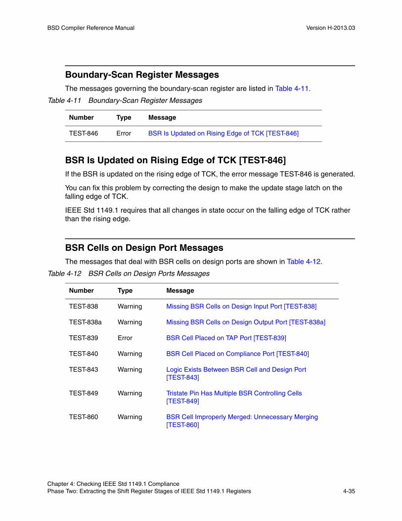
BSD Compiler Reference Manual Version H-2013.03
Boundary-Scan Register MessagesThe messages governing the boundary-scan register are listed in Table 4-11.
BSR Is Updated on Rising Edge of TCK [TEST-846]If the BSR is updated on the rising edge of TCK, the error message TEST-846 is generated.
You can fix this problem by correcting the design to make the update stage latch on the falling edge of TCK.
IEEE Std 1149.1 requires that all changes in state occur on the falling edge of TCK rather than the rising edge.
BSR Cells on Design Port MessagesThe messages that deal with BSR cells on design ports are shown in Table 4-12.
Table 4-11 Boundary-Scan Register Messages
Number Type Message
TEST-846 Error BSR Is Updated on Rising Edge of TCK [TEST-846]
Table 4-12 BSR Cells on Design Ports Messages
Number Type Message
TEST-838 Warning Missing BSR Cells on Design Input Port [TEST-838]
TEST-838a Warning Missing BSR Cells on Design Output Port [TEST-838a]
TEST-839 Error BSR Cell Placed on TAP Port [TEST-839]
TEST-840 Warning BSR Cell Placed on Compliance Port [TEST-840]
TEST-843 Warning Logic Exists Between BSR Cell and Design Port [TEST-843]
TEST-849 Warning Tristate Pin Has Multiple BSR Controlling Cells [TEST-849]
TEST-860 Warning BSR Cell Improperly Merged: Unnecessary Merging [TEST-860]
Chapter 4: Checking IEEE Std 1149.1 Compliance Phase Two: Extracting the Shift Register Stages of IEEE Std 1149.1 Registers 4-35Chapter 4: Checking IEEE Std 1149.1 Compliance Phase Two: Extracting the Shift Register Stages of IEEE Std 1149.1 Registers 4-35

BSD Compiler Reference Manual H-2013.03BSD Compiler Reference Manual Version H-2013.03
Missing BSR Cells on Design Input Port [TEST-838]IEEE Std 1149.1 requires that one or more boundary-scan register cells be provided at each system input of the on-chip system logic. If a boundary-scan cell is missing from a design input port, the warning message TEST-838 is generated.
You can fix this problem by providing the missing boundary-scan register cell on this port.
Missing BSR Cells on Design Output Port [TEST-838a]IEEE Std 1149.1 requires one or more boundary-scan register cells to be provided at each system output of the on-chip system logic. If a boundary-scan cell is missing from a design output port, the warning message TEST-838a is generated.
You can fix this problem by providing the missing boundary-scan register cell on this port.
BSR Cell Placed on TAP Port [TEST-839]IEEE Std 1149.1 forbids the placement of boundary-scan register cells on TAP ports, specifically at the TCK, TDI, TDO, TMS, and TRST* ports. If a boundary-scan register is found on one of these ports, the error message TEST-839 is generated.
You can fix this problem by removing the boundary-scan register cell from the TAP port.
TEST-860a Warning BSR Cell Improperly Merged: Too Many Functions [TEST-860a]
TEST-1121 Information Input BSR Cell At Bidirectional Port Not Detected; Missing Control BSR Cell [TEST-1121]
TEST-1122 Information Input BSR Cell Not Detected At Port Due To Pad Not Propagating Data [TEST-1122]
TEST-1123 Information Output BSR Cell Not Detected Because Pad Cannot Propagate Data [TEST-1123]
TEST-1124 Information BSR Cell %s On Port %s Not Detected Because Control Cell Not Found At Port [TEST-1124]
TEST-1125 Information Cannot Find BSR Cell At Port Caused By BSR Cell Update Stage Flip-Flop [TEST-1125]
Table 4-12 BSR Cells on Design Ports Messages (Continued)
Number Type Message
Chapter 4: Checking IEEE Std 1149.1 Compliance Phase Two: Extracting the Shift Register Stages of IEEE Std 1149.1 Registers 4-36

BSD Compiler Reference Manual Version H-2013.03
BSR Cell Placed on Compliance Port [TEST-840]IEEE Std 1149.1 forbids the placement of boundary-scan register cells on compliance ports. If a boundary-scan register cell is found on one of these ports, the error message TEST-840 is generated.
You can fix this problem by removing the boundary-scan register cell from the compliance port.
Logic Exists Between BSR Cell and Design Port [TEST-843]IEEE Std 1149.1 forbids the placement of logic between the design port and its corresponding BSR cell. If logic is found between these two entities, the warning message TEST-843 is generated.
You can fix this problem by removing the logic between the boundary-scan register cell and the design port.
Tristate Pin Has Multiple BSR Controlling Cells [TEST-849]IEEE Std 1149.1 requires that pad cells not be controlled by multiple BSR cells. If multiple BSR cells drive the controlling input to a pad cell, the warning message TEST-849 is generated.
You can correct this problem by fixing the logic.
BSR Cell Improperly Merged: Unnecessary Merging [TEST-860]If a BSR cell is merged unnecessarily—as in the case where an input is used solely as a control or output source, and not as an input source—IEEE Std 1149.1 states that a single cell can be provided to meet the rules for the input and the output pins. If such a condition is discovered in your logic, the warning message TEST-860 is generated.
You can fix this problem by correcting the BSR cell design.
BSR Cell Improperly Merged: Too Many Functions [TEST-860a]IEEE Std 1149.1 requires that a merged BSR cell not contain more than two functions. If a merged BSR cell controls more than one output port or contains more than two functions, the warning message TEST-860a is generated.
You can fix this problem by limiting the number of output ports driven by the BSR cell to one, or by limiting the number of functions on the merged cell to two.
Chapter 4: Checking IEEE Std 1149.1 Compliance Phase Two: Extracting the Shift Register Stages of IEEE Std 1149.1 Registers 4-37Chapter 4: Checking IEEE Std 1149.1 Compliance Phase Two: Extracting the Shift Register Stages of IEEE Std 1149.1 Registers 4-37

BSD Compiler Reference Manual H-2013.03BSD Compiler Reference Manual Version H-2013.03
Input BSR Cell At Bidirectional Port Not Detected; Missing Control BSR Cell [TEST-1121]Due to a missing BSR cell at the output side of the port, the input BSR cell at a bidirectional port is not detected. If a missing BSR cell on the output causes the input BSR cell to go undetected, the information message TEST-1121 is generated.
You can fix this problem by either inserting a control BSR cell at the output side of the port, or disable the output side of the port and then rerun check_bsd.
Input BSR Cell Not Detected At Port Due To Pad Not Propagating Data [TEST-1122]Because data is stuck at the input pad, the data won’t propagate and therefore the input BSR cell is not detected. Because the data is stuck at the input pad making the input BSR cell undetectable, the information message TEST-1122 is generated and displays the value at the pad pins.
You can fix this correcting the problem in your design at the input pad and then rerun check_bsd.
Output BSR Cell Not Detected Because Pad Cannot Propagate Data [TEST-1123]The output BSR cell isn’t detected because the pad can’t propagate data. When data coming from the output BSR cell gets stuck at the output pad the information message TEST-1123 is generated and displays the value at the pad pins.
You can fix this correcting the problem in your design at the output pad and then rerun check_bsd.
BSR Cell %s On Port %s Not Detected Because Control Cell Not Found At Port [TEST-1124]The BSR cell at the specified port isn’t detected because of a missing control BSR. When the output BSR cell is found to be missing at the port due to a missing control BSR the information message TEST-1124 is generated.
You can fix this problem by inserting a control BSR cell at the output port and then rerun check_bsd.
Chapter 4: Checking IEEE Std 1149.1 Compliance Phase Two: Extracting the Shift Register Stages of IEEE Std 1149.1 Registers 4-38

BSD Compiler Reference Manual Version H-2013.03
Cannot Find BSR Cell At Port Caused By BSR Cell Update Stage Flip-Flop [TEST-1125]The BSR cell at the specified port isn’t detected is caused by the BSR cell update stage flip-flop. When the BSR cell is determined to be missing at the port due to the BSR cell update stage flip-flop the information message TEST-1125 is generated.
Phase Three: Extracting Implemented Instructions and Test Data Registers
You can either allow BSD Compiler to extract the implemented instructions, or you can define the instructions and opcodes explicitly.
Phase Three performs the following tasks when BSD Compiler extracts the implemented instructions automatically:
• Finds the different signatures
• Finds the corresponding set of opcodes
• Infers the SAMPLE and PRELOAD instructions
• Infers all implemented INTEST, RUNBIST, HIGHZ, CLAMP, IDCODE, and USERCODE instructions
Alternatively, you can specify all the instructions and the corresponding opcodes manually by using the command check_bsd -infer_instructions false:
• Specify the different implemented instructions
• Specify their corresponding set of opcodes
You specify these instructions and opcodes using the set_bsd_instruction command.
Phase Three performs the following tasks when either BSD Compiler extracts the implemented instructions or when you define the instructions and opcodes:
• Extracts the decoding logic
• Identifies the test data register selected by each signature
• Characterizes each signature’s behavior
• Infers primary inputs and primary outputs for all BSR cells
In the next section, a detailed discussion of the phase three checks is presented. Messages addressing phase three violations are discussed in the sections that follow.
Chapter 4: Checking IEEE Std 1149.1 Compliance Phase Three: Extracting Implemented Instructions and Test Data Registers 4-39Chapter 4: Checking IEEE Std 1149.1 Compliance Phase Three: Extracting Implemented Instructions and Test Data Registers 4-39

BSD Compiler Reference Manual H-2013.03BSD Compiler Reference Manual Version H-2013.03
Phase Three ProcessPhase Three checks are performed in the manner discussed in the following sections.
Extracting Decoding PinsThe check_bsd command extracts the different decoding pins. The decoding pins control the behavior of the boundary-scan logic. The expected value for the set of pins is called a signature. The signature represents the independent state of the instruction decoding logic.
...finding the set of IR decoding pins
Decoding pins are shown in Figure 4-8.
Figure 4-8 Decoding Pins
Boundary-Scan Register
Bypass Register
User Test Data Register
TDO
TAPController
Instruction Register
Chapter 4: Checking IEEE Std 1149.1 Compliance Phase Three: Extracting Implemented Instructions and Test Data Registers 4-40

BSD Compiler Reference Manual Version H-2013.03
Building an Opcode SetAn opcode is the string of bits shifted into the shift register stage of the instruction register. When that opcode is shifted in, a relationship is defined between the signatures and their corresponding opcodes.
The check_bsd command builds the set of opcodes. Each opcode set is characterized by a unique signature.
Analyzing and Classifying SignaturesBefore check_bsd can infer instructions, it must first analyze and classify each signature’s behavior.
The check_bsd command performs the following tasks with the signatures:
• Looks at what register is selected when a signature is shifted in
• Classifies the signature according to the test data register it is selecting
...Analyzing the different signatures at the decoding pin
• Classifies the signature according to the output conditioning of the instructions:
❍ Instructions that condition the outputs: INTEST, RUNBIST, EXTEST, CLAMP, HIGHZ
❍ Instructions that don’t condition the outputs: SAMPLE, PRELOAD, BYPASS, IDCODE
...Checking output conditioning of the implemented instruction
• Classifies the boundary-scan register signatures according to the value captured into and applied by the boundary-scan register
• By cross-referencing the signature classifications produced in this process, check_bsd can infer instructions
Inferring the SAMPLE and PRELOAD InstructionsMaking use of the signature classifications, check_bsd shifts an opcode corresponding to SAMPLE and PRELOAD into the instruction register.
The check_bsd command infers the SAMPLE and PRELOAD instructions as follows:
• Infers the SAMPLE instruction when the input BSR cell’s shift elements capture the data input value at the rising TCK in the capture-DR state.
• Infers the PRELOAD instruction when the output BSR cell’s update elements load the data held in the associated shift register stage at the falling TCK in the update-DR state.
Chapter 4: Checking IEEE Std 1149.1 Compliance Phase Three: Extracting Implemented Instructions and Test Data Registers 4-41Chapter 4: Checking IEEE Std 1149.1 Compliance Phase Three: Extracting Implemented Instructions and Test Data Registers 4-41

BSD Compiler Reference Manual H-2013.03BSD Compiler Reference Manual Version H-2013.03
The check_bsd command must identify the primary inputs and primary outputs for each boundary-scan register cell so that the boundary-scan register cells can be delineated from the rest of the design logic.
The check_bsd command uses a tracing mechanism to determine the pins associated with the primary inputs and the primary outputs of each given boundary-scan register cell.
...finding controlling BSR cells PIs
...finding controlling BSR cells POs
...finding non-controlling BSR cells PIs
...finding BSR cell POs
The check_bsd command uses an algorithm to search for feedthroughs. If there is a feed-through problem, check_bsd must recompute the structure to determine the real primary input.
... Modifying controlling/outputs BSR cell PIs
There are no numbered messages associated with the feedthrough checking portion of check_bsd.
Any violations that occur during the inference of the SAMPLE and PRELOAD instructions are flagged with messages described “SAMPLE and PRELOAD Instruction Messages” on page 4-43.
Inferring Other InstructionsThe check_bsd command looks for the INTEST instruction, to see whether it is implemented or not.
...inferring the implemented INTEST instruction
If the INTEST instruction is implemented, it corresponds to a given set of opcodes shifted into the instruction register (provided that the outputs are conditioned and that the selected test data register is the boundary-scan register).
There are no numbered messages associated with the INTEST inference checking portion of check_bsd.
If the outputs are conditioned to something other than high impedance, and the test-data-register selected is the bypass register, the corresponding instruction is set to CLAMP.
...inferring the implemented CLAMP instruction
If the outputs are conditioned to high impedance and the test-data-register selected is the bypass register, the corresponding instruction is set to HIGHZ.
...Inferring the implemented HIGHZ instruction
Chapter 4: Checking IEEE Std 1149.1 Compliance Phase Three: Extracting Implemented Instructions and Test Data Registers 4-42

BSD Compiler Reference Manual Version H-2013.03
If the current opcode is the same as the one loaded during the Test-Logic-Reset state of TAP controller, the instruction is set to IDCODE. Otherwise the instruction is set to USERCODE.
...inferring the implemented IDCODE & USERCODE instruction
If the outputs are conditioned to HIGHZ and the test data register selected is a user-defined register, the instruction is set to RUNBIST.
...inferring the implemented RUNBIST instruction
At this point each opcode should have an associated instruction. The next step is to analyze the behavior of the boundary-scan register for the instruction that is selected.
SAMPLE and PRELOAD Instruction MessagesTo analyze the instructions in detail and to analyze the characteristics of BSR cells, the primary inputs and primary outputs of the cells are inferred.
Problems are governed by the messages listed in Table 4-13 and discussed in the sections that follow.
Table 4-13 Parallel Input and Output Messages
Number Type Message
TEST-837 Warning Opcode Does Not Select Register [TEST-837]
TEST-841 Error Missing SAMPLE/PRELOAD Instruction [TEST-841]
TEST-875 Warning BSR Cell Cannot Capture Logic State of Input Port [TEST-875]
TEST-890 Warning Unable to Locate Parallel Input for BSR Cell [TEST-890]
TEST-891 Error Unable to Locate Parallel Output for BSR Cell [TEST-891]
TEST-896 Error Mandatory SAMPLE Instruction Not Implemented [TEST-896]
TEST-897 Error Mandatory PRELOAD Instruction Not Implemented [TEST-897]
Chapter 4: Checking IEEE Std 1149.1 Compliance Phase Three: Extracting Implemented Instructions and Test Data Registers 4-43Chapter 4: Checking IEEE Std 1149.1 Compliance Phase Three: Extracting Implemented Instructions and Test Data Registers 4-43

BSD Compiler Reference Manual H-2013.03BSD Compiler Reference Manual Version H-2013.03
Opcode Does Not Select Register [TEST-837]A register must be selected with any opcode instruction. IEEE Std 1149.1 requires that all unused opcodes be set to select the bypass register. If an opcode fails to select any register, the warning message TEST-837 is generated.
You can fix this problem by mapping the opcode to select the bypass register if it is otherwise unused. If it is used for another register, correct the design to select the proper register.
Missing SAMPLE/PRELOAD Instruction [TEST-841]SAMPLE/PRELOAD is an instruction mandated by IEEE Std 1149.1. If the instruction is not found during the inferring process, the message TEST-841 is generated.
BSR Cell Cannot Capture Logic State of Input Port [TEST-875]If, during the inference of a SAMPLE/PRELOAD instruction, some BSR cells cannot capture the data on their design input ports, the warning message TEST-875 is generated.
This problem might be caused by one of the following:
• The instruction might not be SAMPLE/PRELOAD, but instead a private instruction.
• The design of SAMPLE/PRELOAD might be incorrect.
• The BSR cell design might be incorrect.
If this instruction is private, you can ignore the warning. If it is not private, you must correct the design problem.
Unable to Locate Parallel Input for BSR Cell [TEST-890]If no primary input is discovered on a BSR cell, the warning message TEST-890 is generated.
The reason for not finding a primary input of an observable or controllable BSR cell can be one of the following:
• BSR cell is not compliant to IEEE Std 1149.1 because its primary input does not drive its primary output during SAMPLE/PRELOAD.
• The primary input is not captured into the shift register stage properly.
You can fix this problem by correcting the BSR cell implementation if you want to check for further compliance. No BSDL can be generated if this problem is not addressed.
Chapter 4: Checking IEEE Std 1149.1 Compliance Phase Three: Extracting Implemented Instructions and Test Data Registers 4-44

BSD Compiler Reference Manual Version H-2013.03
Unable to Locate Parallel Output for BSR Cell [TEST-891]If no primary output is discovered on a BSR cell, the warning message TEST-891 is generated.
The reason for not finding a primary output of an observable or controllable BSR cell can be one of the following:
• BSR cell is not compliant to IEEE Std 1149.1 because its primary output is not driven by its primary input during SAMPLE/PRELOAD
• The primary output is not captured into the shift register stage properly
You can fix this problem by correcting the BSR cell implementation if you want to check for further compliance. No BSDL can be generated if this problem is not addressed.
Mandatory SAMPLE Instruction Not Implemented [TEST-896]This error assumes you are working within the IEEE Standard 1149.1(2001) guidelines and occurs during check_bsd when you have not specified the SAMPLE instruction. Each component must be accompanied with a SAMPLE instruction, which is inferred by analyzing input port capture by the boundary-scan register cells on the design input ports.
To fix this error, ensure that you have specified the correct opcodes for the implemented SAMPLE instruction and that the design implements the SAMPLE instruction correctly. If you do not know the SAMPLE instruction opcodes, specify check_bsd -infer_instructions and then rerun check_bsd.
Mandatory PRELOAD Instruction Not Implemented [TEST-897]This error assumes you are working within the IEEE Standard 1149.1(2001) guidelines and occurs during check_bsd when you have not specified the PRELOAD instruction. Each component must be accompanied with a PRELOAD instruction, which is inferred by analyzing the update behavior of the boundary-scan register. The output update flip-flops should load the data held in the associated shift register cells on the falling edge of TCK in the UPDATE-DR state.
To fix this error, ensure that you have specified the correct opcodes for the implemented PRELOAD instruction and that the design correctly implements the PRELOAD instruction. If you do not know the PRELOAD instruction opcodes, specify check_bsd -infer_instructions and then rerun check_bsd.
Chapter 4: Checking IEEE Std 1149.1 Compliance Phase Three: Extracting Implemented Instructions and Test Data Registers 4-45Chapter 4: Checking IEEE Std 1149.1 Compliance Phase Three: Extracting Implemented Instructions and Test Data Registers 4-45

BSD Compiler Reference Manual H-2013.03BSD Compiler Reference Manual Version H-2013.03
Phase Four: Inferring BSR Cell Characteristics
Phase Four performs the following tasks:
• Analyzes all the BSR cells for each inferred instruction
• Characterizes the functionality of each BSR cell with respect to the inferred instructions
• Analyzes the structure of each BSR cell
• Assigns a cell type (BC_0 to BC_7) to individual BSR cells, depending on their functional and structural characteristics
Phase Four verifies the following design elements:
• HIGHZ instruction
• CLAMP instruction
• INTEST instruction
• RUNBIST instruction
• IDCODE and USERCODE instructions
• Operation of BSR at system logic inputs
• Operation of BSR at system logic outputs
• Operation of BSR at system bidirectional (BIDI) signals
• Operation of merged BSR cells
In the next section, a detailed discussion of the phase four checks is discussed. Messages addressing phase four violations are discussed in the sections that follow.
Phase Four ProcessPhase Four checks occur in the following sequence.
Analyzing SAMPLE and PRELOAD RulesAfter the real primary input and primary output are found, some basic rules are checked if the SAMPLE and PRELOAD instructions are active.
Chapter 4: Checking IEEE Std 1149.1 Compliance Phase Four: Inferring BSR Cell Characteristics 4-46

BSD Compiler Reference Manual Version H-2013.03
These rules include
• Transparency
• The signal flowing through the logic outpu77t to be captured at the output BSR
• System input value to be captured on the input BSR
BSD Compiler analyzes the SAMPLE and PRELOAD instructions as follows:
• SAMPLE binary codes are checked to ensure that the capture descriptor is legal and that BSR cell data sources are PI for all BSR cells.
• PRELOAD binary codes are checked to ensure that the BSR cells’ update elements load the data values held in their associated shift element on the falling edge of TCK in the Update-DR controller state.
Characterizing the Cell BehaviorThe cell behavior is characterized for the given instruction according to the IEEE Std 1149.1.
...Analyzing INTEST instruction
...Analyzing CLAMP instruction
...Analyzing HIGHZ instruction
...Analyzing the EXTEST instruction
For each BSR cell, the type of BC cell is determined (BC_1 to BC_7). This information is then passed on to the BSDL generation process.
Invalid Capture Descriptor for Instruction (Nonspecific)IEEE Std 1149.1 requires that the signal loaded into the shift register stage of each BSR cell on the rising edge of TCK in the Capture_DR controller state be mapped to a particular cell at the system logic output.
Mismatched BSR Cell Mapping [TEST-871]If the BSR cell to system logic output cell mapping does not match the mapping discovered by the tool, the error message TEST-871 is generated (see Table 4-14).
Table 4-14 General Instruction Messages
Number Type Message
TEST-871 Error Invalid Capture Descriptor for Instruction (Nonspecific)
Chapter 4: Checking IEEE Std 1149.1 Compliance Phase Four: Inferring BSR Cell Characteristics 4-47Chapter 4: Checking IEEE Std 1149.1 Compliance Phase Four: Inferring BSR Cell Characteristics 4-47
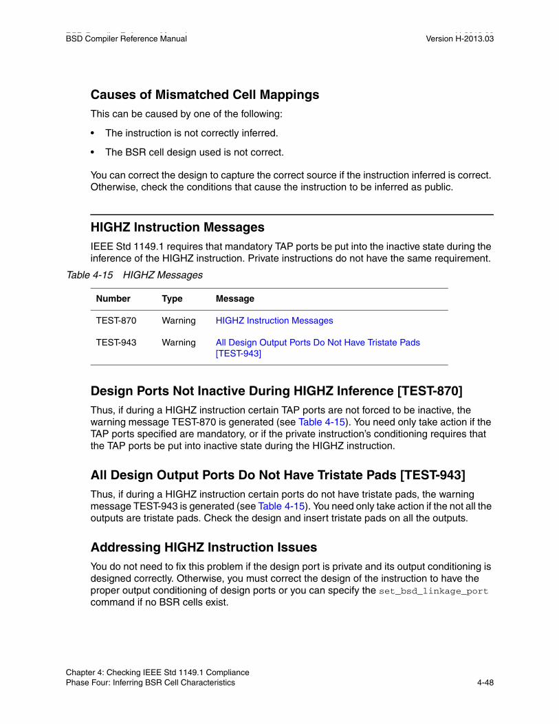
BSD Compiler Reference Manual H-2013.03BSD Compiler Reference Manual Version H-2013.03
Causes of Mismatched Cell MappingsThis can be caused by one of the following:
• The instruction is not correctly inferred.
• The BSR cell design used is not correct.
You can correct the design to capture the correct source if the instruction inferred is correct. Otherwise, check the conditions that cause the instruction to be inferred as public.
HIGHZ Instruction MessagesIEEE Std 1149.1 requires that mandatory TAP ports be put into the inactive state during the inference of the HIGHZ instruction. Private instructions do not have the same requirement.
Design Ports Not Inactive During HIGHZ Inference [TEST-870]Thus, if during a HIGHZ instruction certain TAP ports are not forced to be inactive, the warning message TEST-870 is generated (see Table 4-15). You need only take action if the TAP ports specified are mandatory, or if the private instruction’s conditioning requires that the TAP ports be put into inactive state during the HIGHZ instruction.
All Design Output Ports Do Not Have Tristate Pads [TEST-943]Thus, if during a HIGHZ instruction certain ports do not have tristate pads, the warning message TEST-943 is generated (see Table 4-15). You need only take action if the not all the outputs are tristate pads. Check the design and insert tristate pads on all the outputs.
Addressing HIGHZ Instruction IssuesYou do not need to fix this problem if the design port is private and its output conditioning is designed correctly. Otherwise, you must correct the design of the instruction to have the proper output conditioning of design ports or you can specify the set_bsd_linkage_port command if no BSR cells exist.
Table 4-15 HIGHZ Messages
Number Type Message
TEST-870 Warning HIGHZ Instruction Messages
TEST-943 Warning All Design Output Ports Do Not Have Tristate Pads [TEST-943]
Chapter 4: Checking IEEE Std 1149.1 Compliance Phase Four: Inferring BSR Cell Characteristics 4-48

BSD Compiler Reference Manual Version H-2013.03
CLAMP Instruction MessagesThe CLAMP instruction error messages are shown in Table 4-16.
BSR Updates Under CLAMP Instruction [TEST-847]IEEE Std 1149.1 requires that all latched output of the BSR should retain their states until one of the following conditions occurs:
• The Test-Logic-Reset controller state is entered as a result of the application of a logic 0 at TRST*.
• The first falling edge of TCK occurs in Test-Logic-Reset controller state when that state is entered as a result of signals applied at TCK and TMS.
If the BSR updates improperly when either of the aforementioned conditions has not been met, the warning message TEST-847 is generated.
You can fix this problem by making the update stage static during the CLAMP instruction.
Port Not Driven by BSR Cell for Opcode During CLAMP [TEST-874]During the inference of the CLAMP instruction, for any nonprivate opcode, all boundary-scan cells need to drive their respective design ports. If any BSR cells fail to drive their design ports, whether public or private, the warning message TEST-874 is generated.
This might be caused by one of the following conditions:
• The instruction is not CLAMP, but a private instruction
• The design of the CLAMP instruction is incorrect
If the instruction opcode belongs to a private instruction, ignore the warning. Otherwise, you must correct the design of CLAMP to cause all design ports to be driven by BSR cells.
Table 4-16 CLAMP Messages
Number Type Message
TEST-847 Warning BSR Updates Under CLAMP Instruction [TEST-847]
TEST-874 Warning Port Not Driven by BSR Cell for Opcode During CLAMP [TEST-874]
TEST-1133 Information Port Not Driven Or Captured by BSR [TEST-1133]
TEST-1136 Information List Of Update Flip-Flops Reset Illegally [TEST-1136]
Chapter 4: Checking IEEE Std 1149.1 Compliance Phase Four: Inferring BSR Cell Characteristics 4-49Chapter 4: Checking IEEE Std 1149.1 Compliance Phase Four: Inferring BSR Cell Characteristics 4-49
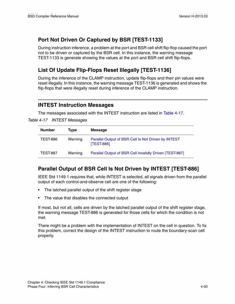
BSD Compiler Reference Manual H-2013.03BSD Compiler Reference Manual Version H-2013.03
Port Not Driven Or Captured by BSR [TEST-1133]During instruction inference, a problem at the port and BSR cell shift flip-flop caused the port not to be driven or captured by the BSR cell. In this instance, the warning message TEST-1133 is generate showing the values at the port and BSR cell shift flip-flops.
List Of Update Flip-Flops Reset Illegally [TEST-1136]During the inference of the CLAMP instruction, update flip-flops and their pin values were reset illegally. In this instance, the warning message TEST-1136 is generated and shows the flip-flops that were illegally reset during inference of the CLAMP instruction.
INTEST Instruction MessagesThe messages associated with the INTEST instruction are listed in Table 4-17.
Parallel Output of BSR Cell Is Not Driven by INTEST [TEST-886]IEEE Std 1149.1 requires that, while INTEST is selected, all signals driven from the parallel output of each control-and-observe cell are one of the following:
• The latched parallel output of the shift register stage
• The value that disables the connected output
If most, but not all, cells are driven by the latched parallel output of the shift register stage, the warning message TEST-886 is generated for those cells for which the condition is not met.
There might be a problem with the implementation of INTEST on the cell in question. To fix this problem, correct the design of the INTEST instruction to route the boundary-scan cell properly.
Table 4-17 INTEST Messages
Number Type Message
TEST-886 Warning Parallel Output of BSR Cell Is Not Driven by INTEST [TEST-886]
TEST-887 Warning Parallel Output of BSR Cell Invalidly Driven [TEST-887]
Chapter 4: Checking IEEE Std 1149.1 Compliance Phase Four: Inferring BSR Cell Characteristics 4-50

BSD Compiler Reference Manual Version H-2013.03
Parallel Output of BSR Cell Invalidly Driven [TEST-887]IEEE Std 1149.1 states that for clock inputs, when the INTEST instruction is selected, the signal driven to the on-chip system logic shall be one of the following:
• The signal received at the connected system pin
• The TCK signal, controlled such that the on-chip system logic changes state only in the Run-Test/Idle controller state
• The parallel output of the shift register stage
If the parallel output of a clock boundary-scan cell is not driven according to one of the conditions previously noted, the warning message TEST-887 is generated.
You can fix this problem by correcting the INTEST routing for the BSR cell on the clock system pins.
RUNBIST Instruction MessagesIEEE Std 1149.1 requires that all latched output of the BSR retain their states until one of the following conditions occurs:
• The Test-Logic-Reset controller state is entered as a result of the application of a logic 0 at TRST*.
• The first falling edge of TCK occurs in Test-Logic-Reset controller state when that state is entered as a result of signals applied at TCK and TMS.
BSR Updates Improperly [TEST-848]If the BSR updates improperly when either of the aforementioned conditions has not been met, the warning message TEST-848 is generated.
Addressing RUNBIST IssuesYou can fix this problem by making the update stage static during the RUNBIST instruction.
Table 4-18 RUNBIST Messages
Number Type Message
TEST-848 Warning BSR Updates Improperly [TEST-848]
Chapter 4: Checking IEEE Std 1149.1 Compliance Phase Four: Inferring BSR Cell Characteristics 4-51Chapter 4: Checking IEEE Std 1149.1 Compliance Phase Four: Inferring BSR Cell Characteristics 4-51

BSD Compiler Reference Manual H-2013.03BSD Compiler Reference Manual Version H-2013.03
EXTEST Instruction MessagesThe messages that govern the EXTEST instruction are listed in Table 4-19.
EXTEST Opcode Is Not Specified [TEST-820]This error assumes you are working within the IEEE Standard 1149.1(2001) guidelines and occurs during check_bsd when you have not specified the opcode for the EXTEST instruction. You must explicitly specify the EXTEST opcode using the set_bsd_instruction command.
Invalid Capture Source for EXTEST Instruction [TEST-872]IEEE Std 1149.1 requires the signal loaded into the shift register stage of each design input port on the rising edge of TCK to be driven from an external source. The signal must be received from the primary system logic input. If the signal comes from any other source, the warning message TEST-872 is generated.
You can fix this by correcting the design of the BSR cell on the design input.
Invalid Output Conditioning During EXTEST [TEST-873]IEEE Std 1149.1 states that the signal driven from the parallel output of each control-and-observe cell in EXTEST should be the parallel output of the shift-register stage. If, when EXTEST is inferred, some BSR cells are not driven by latched parallel outputs, the error message TEST-873 is generated.
You must fix this error condition by correcting the design of the EXTEST instruction or of the BSR cell at the system outputs.
Table 4-19 EXTEST Messages
Number Type Message
TEST-820 Error EXTEST Opcode Is Not Specified [TEST-820]
TEST-872 Warning Invalid Capture Source for EXTEST Instruction [TEST-872]
TEST-873 Error Invalid Output Conditioning During EXTEST [TEST-873]
TEST-876 Error BSR Cell Output Not Driven by Update Flip-Flop in EXTEST [TEST-876]
TEST-1128 Information Ports Not Being Driven by Their BSR Cell Shift Stage [TEST-1128]
Chapter 4: Checking IEEE Std 1149.1 Compliance Phase Four: Inferring BSR Cell Characteristics 4-52
BSD Compiler Reference Manual Version H-2013.03
BSR Cell Output Not Driven by Update Flip-Flop in EXTEST [TEST-876]IEEE Std 1149.1 states that when EXTEST is selected, the state of all signals driven from system output pins shall be completely defined by the data held in the BSR and change only on the falling edge of TCK in the Update_DR controller state. If the output pin of a BSR cell is not driven by the update flip-flop during the EXTEST instruction, the error message TEST-876 is generated.
You must fix this problem by correcting the design of EXTEST in the circuit.
Ports Not Being Driven by Their BSR Cell Shift Stage [TEST-1128]There is illegal output conditioning on the output BSR cells during EXTEST. Because ports are not driven by their BSR cell during the shift stage the information message TEST-1123 is generated and displays the port on which this occurred.
Input and Output Cell MessagesThe messages that govern the BSR input cells and output cells are listed in Table 4-20.
Output Pins Not Driven by Input Pins During Instruction [TEST-877]During certain instructions—specifically SAMPLE, PRELOAD, BYPASS, IDCODE, and USERCODE—the operation of the test logic has no effect on the operation of the on-chip system logic or on the flow of signals between system pins and on-chip system logic. Consequently, the output pin of a BSR cell must be driven directly by its input pin. If this is not the case, the warning message TEST-877 is generated.
This condition might be caused by one of the following issues:
• The BSR cell does not allow the primary input to be driven by the primary output.
• The design of the instruction with this opcode is incorrect.
You can fix this by correcting the design problem.
Table 4-20 Input and Output Cell Messages
Number Type Message
TEST-877 Warning Output Pins Not Driven by Input Pins During Instruction [TEST-877]
TEST-878 Warning BSR Cell Capture Value Is Not From Input Pin [TEST-878]
Chapter 4: Checking IEEE Std 1149.1 Compliance Phase Four: Inferring BSR Cell Characteristics 4-53Chapter 4: Checking IEEE Std 1149.1 Compliance Phase Four: Inferring BSR Cell Characteristics 4-53

BSD Compiler Reference Manual H-2013.03BSD Compiler Reference Manual Version H-2013.03
BSR Cell Capture Value Is Not From Input Pin [TEST-878]If, during inference, the primary input to a BSR cell cannot be found, the error message TEST-878 is generated. As a result of this error, no further processing can occur on the design. The check_bsd command can to find the cause of the problem.
To fix this problem, run check_bsd in verbose mode to isolate the problem. Correct the cause of the problem before you continue.
Cell Type MessagesThe messages that govern the types of cells in the boundary-scan design are listed in Table 4-21.
Invalid Number of Capture Descriptors [TEST-882]A BSR cell type can be from of BC_0 to BC_7. For you to assign a particular type to the appropriate cell, a number of capture descriptors need to be present for each EXTEST, INTEST, SAMPLE, or PRELOAD instruction associated with that cell. If an insufficient number of capture descriptors are present for a particular cell, the warning message TEST-882 is generated.
This problem highlights a problem in analyzing the mandatory instructions EXTEST, SAMPLE, and PRELOAD.
Table 4-21 Cell Types
Number Type Message
TEST-882 Warning Invalid Number of Capture Descriptors [TEST-882]
TEST-889 Warning BSR Cell Is Not Standard Type [TEST-889]
TEST-898 Error BSR Cell Not a Valid Cell Type [TEST-898]
TEST-1129 Information Capture Descriptor Found for BSR Cell [TEST-1129]
TEST-1129a Information Illegal Capture Descriptor for BSR Cell [TEST-1129a]
TEST-1130 Information INTEST Not Supported on Input of BC_4 BSR Cell [TEST-1130]
TEST-1131 Information INTEST Not Supported on Two-state Output of BC_4 BSR Cell [TEST-1131]
Chapter 4: Checking IEEE Std 1149.1 Compliance Phase Four: Inferring BSR Cell Characteristics 4-54

BSD Compiler Reference Manual Version H-2013.03
Fix this problem by reviewing the analysis of the mandatory instructions and fixing other, associated problems.
BSR Cell Is Not Standard Type [TEST-889]According to IEEE Std 1149.1, to differentiate cell types from BC_0 through BC_7, the BSR cells on system inputs and outputs are analyzed under the influence of the EXTEST, SAMPLE, PRELOAD, and INTEST instructions to find the captured source. The BSR cells are then structurally analyzed to find other characteristics. The information gathered determines what cell type is to be assigned to the BSR cell. If the analysis determines the cells to have characteristics other than those appropriate to the specific cell types BC_0 to BC_7, the cell is determined to be nonstandard.
If this situation occurs on a BSR cell in your design, the cell type is defaulted to be BC_0 and the warning message TEST-889 is generated.
You should check the analysis of the EXTEST, SAMPLE, PRELOAD, and INTEST instructions to determine what functional problems, if any, exist.
BSR Cell Not a Valid Cell Type [TEST-898]IEEE Std 1149.1 states that the only valid cell types allowed are the following:
• INPUT
• OUTPUT2
• CLOCK
• OUTPUT3
• CONTROL
• CONTROLR
• INTERNAL
• BIDIR
• OBSERVE_ONLY
If the cell type is not one of those listed, the error message TEST-898 is generated.
You must fix the design and functionality of the BSR cells.
Chapter 4: Checking IEEE Std 1149.1 Compliance Phase Four: Inferring BSR Cell Characteristics 4-55Chapter 4: Checking IEEE Std 1149.1 Compliance Phase Four: Inferring BSR Cell Characteristics 4-55

BSD Compiler Reference Manual H-2013.03BSD Compiler Reference Manual Version H-2013.03
Capture Descriptor Found for BSR Cell [TEST-1129]According to IEEE Std 1149.1, capture descriptors of a BSR cell are a set of triplets, showing the behavior of the BSR cell under the standard instructions, in the following form:
(<BSR Cell Content>, <Capture Instruction>, <Data Source for the value captured in the cell>)
If BSD Compiler finds a capture descriptor for the BSR cell, creating a nonstandard BSR cell, the information message TEST-1129 is generated.
You should verify that the BSR cell design is compliant with the standard and that the BSR cell type is appropriate for the instructions you implement.
Illegal Capture Descriptor for BSR Cell [TEST-1129a]According to IEEE Std 1149.1, capture descriptors of a BSR cell are a set of triplets, showing the behavior of the BSR cell under the standard instructions, in the following form:
(<BSR Cell Content>, <Capture Instruction>, <Data Source for the value captured in the cell>).
If BSD Compiler finds an illegal capture descriptor for the BSR cell, the information message TEST-1129a is generated.
You should verify that the BSR cell design is compliant with the standard and that the BSR cell type is appropriate for the instructions you implement.
INTEST Not Supported on Input of BC_4 BSR Cell [TEST-1130]The INTEST instruction is not supported as an input by a BC_4 type BSR cell. Implementing an INTEST instruction at this point causes a nonstandard BSR cell.
As the INTEST instruction is implemented, an input BSR cell is found to be of type BC_0 instead of BC_4, thereby generating information message TEST-1130. You should verify that the BSR cell design is compliant with the standard and that the BSR cell type is appropriate for the instructions you implement.
INTEST Not Supported on Two-state Output of BC_4 BSR Cell [TEST-1131]The INTEST instruction is not supported on a two-state output by a BC_4 type BSR cell. Implementing an INTEST instruction at this point causes a nonstandard BSR cell.
As the INTEST instruction is implemented, an output2 BSR cell is found to be of type BC_0 instead of BC_2, thereby generating the information message TEST-1131.
Chapter 4: Checking IEEE Std 1149.1 Compliance Phase Four: Inferring BSR Cell Characteristics 4-56
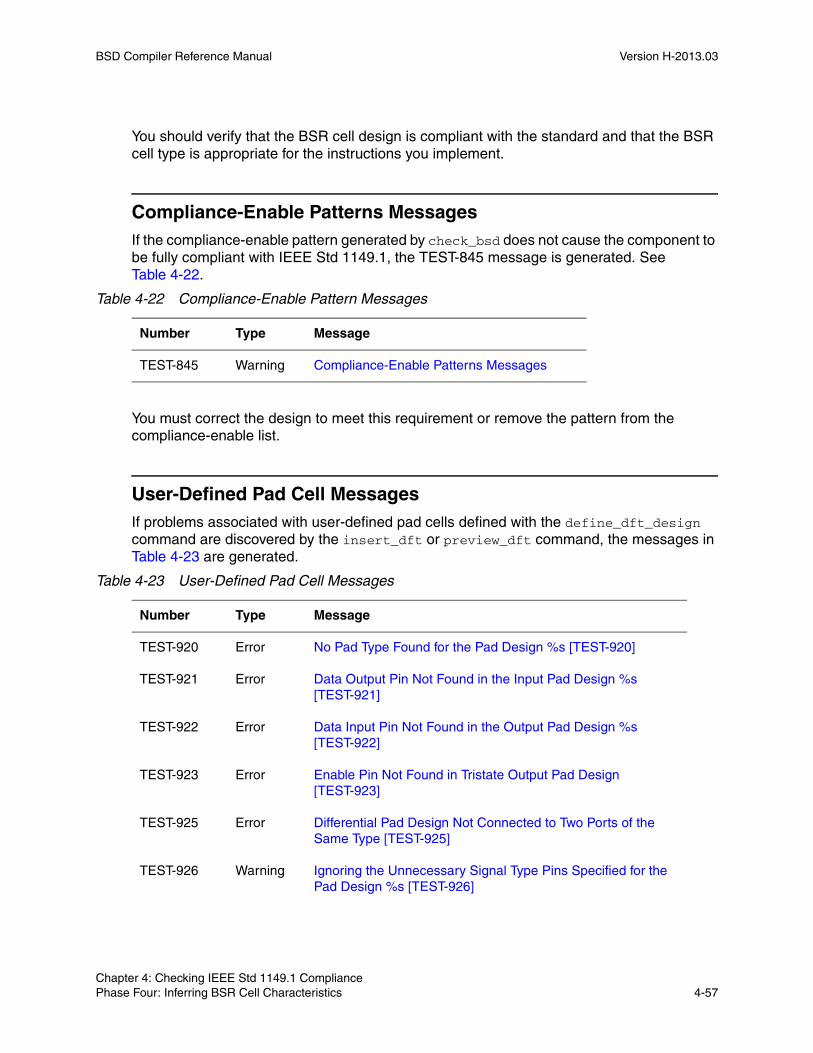
BSD Compiler Reference Manual Version H-2013.03
You should verify that the BSR cell design is compliant with the standard and that the BSR cell type is appropriate for the instructions you implement.
Compliance-Enable Patterns MessagesIf the compliance-enable pattern generated by check_bsd does not cause the component to be fully compliant with IEEE Std 1149.1, the TEST-845 message is generated. See Table 4-22.
You must correct the design to meet this requirement or remove the pattern from the compliance-enable list.
User-Defined Pad Cell MessagesIf problems associated with user-defined pad cells defined with the define_dft_design command are discovered by the insert_dft or preview_dft command, the messages in Table 4-23 are generated.
Table 4-22 Compliance-Enable Pattern Messages
Number Type Message
TEST-845 Warning Compliance-Enable Patterns Messages
Table 4-23 User-Defined Pad Cell Messages
Number Type Message
TEST-920 Error No Pad Type Found for the Pad Design %s [TEST-920]
TEST-921 Error Data Output Pin Not Found in the Input Pad Design %s [TEST-921]
TEST-922 Error Data Input Pin Not Found in the Output Pad Design %s [TEST-922]
TEST-923 Error Enable Pin Not Found in Tristate Output Pad Design [TEST-923]
TEST-925 Error Differential Pad Design Not Connected to Two Ports of the Same Type [TEST-925]
TEST-926 Warning Ignoring the Unnecessary Signal Type Pins Specified for the Pad Design %s [TEST-926]
Chapter 4: Checking IEEE Std 1149.1 Compliance Phase Four: Inferring BSR Cell Characteristics 4-57Chapter 4: Checking IEEE Std 1149.1 Compliance Phase Four: Inferring BSR Cell Characteristics 4-57

BSD Compiler Reference Manual H-2013.03BSD Compiler Reference Manual Version H-2013.03
No Pad Type Found for the Pad Design %s [TEST-920]If you fail to specify a pad type for the pad design in the command define_dft_design, this message is generated during the insert_dft or preview_dft command.
You can fix this problem by providing a valid -type PAD value in the define_dft_design command and then rerunning insert_dft or preview_dft.
Data Output Pin Not Found in the Input Pad Design %s [TEST-921]An output pin type, either data_out or data_out_inverted, is expected to be instantiated on an input pad with the define_dft_design command. If the pin type is not instantiated, or if the pin instantiated does not exist, this message is generated during insert_dft or preview_dft.
You can fix this problem by providing a valid pad design pin name for the data_out or data_out_inverted signal type in the access list of the define_dft_design command and then rerunning insert_dft or preview_dft.
Data Input Pin Not Found in the Output Pad Design %s [TEST-922]An input pin type, either data_in or data_in_inverted, is expected to be instantiated on an output pad with the define_dft_design command. If the pin type is not instantiated, or if the pin instantiated does not exist, this message is generated during insert_dft or preview_dft.
You can fix this problem by providing a valid pad design pin name for the data_in or data_in_inverted signal type in the access list of the define_dft_design command and then rerunning insert_dft or preview_dft.
TEST-928 Warning Output Disable Result Value Not Specified for the Tristate Pad Design %s [TEST-928]
TEST-929 Warning Enable Pin Not Found or Not Specified for the Bidirectional Pad Design %s. The Pad Design Will Be Treated As an Open Drain Bidirectional Pad [TEST-929]
Table 4-23 User-Defined Pad Cell Messages (Continued)
Number Type Message
Chapter 4: Checking IEEE Std 1149.1 Compliance Phase Four: Inferring BSR Cell Characteristics 4-58

BSD Compiler Reference Manual Version H-2013.03
Enable Pin Not Found in Tristate Output Pad Design [TEST-923]An enable pin type, either enable or enable_inverted, is expected to be instantiated on a tristate pad with the define_dft_design command. If the pin type is not instantiated or if the pin instantiated does not exist, this message is generated during insert_dft or preview_dft.
You can fix this problem by providing a valid pad design pin name for the enable or enable_inverted signal type in the access list of the define_dft_design command and then rerunning insert_dft or preview_dft.
Differential Pad Design Not Connected to Two Ports of the Same Type [TEST-925]If you specified a pad design that is not connected to two ports of the same type, this message is generated during insert_dft and preview_dft.
You can fix this problem by modifying the design so the differential pad design is connected to two ports of the same type and then rerunning insert_dft or preview_dft.
Ignoring the Unnecessary Signal Type Pins Specified for the Pad Design %s [TEST-926]If you specify signal types that are not required for the pad type you have defined, insert_dft and preview_dft has ignored them and issues this informational message.
Output Disable Result Value Not Specified for the Tristate Pad Design %s [TEST-928]If you do not provide a value for the $disable_res$ parameter, specified with the define_dft_design -params command, this message is generated during insert_dft or preview_dft.
You can fix this problem by providing a disable result value (disable_res) for the define_dft_design command and then rerunning insert_dft or preview_dft.
Enable Pin Not Found or Not Specified for the Bidirectional Pad Design %s. The Pad Design Will Be Treated As an Open Drain Bidirectional Pad [TEST-929]If you do not identify any enable or enable_inverted signal type in the access list of your pad design, or if the pin you have specified is not found in the design, this warning message is generated. The pad design is treated as an open drain bidirectional pad.
If you do not want this pad to be treated as an open drain bidirectional pad, you can correct the define_dft_design specification and rerun insert_dft or preview_dft.
Chapter 4: Checking IEEE Std 1149.1 Compliance Phase Four: Inferring BSR Cell Characteristics 4-59Chapter 4: Checking IEEE Std 1149.1 Compliance Phase Four: Inferring BSR Cell Characteristics 4-59

BSD Compiler Reference Manual H-2013.03BSD Compiler Reference Manual Version H-2013.03
Chapter 4: Checking IEEE Std 1149.1 Compliance Phase Four: Inferring BSR Cell Characteristics 4-60

5Generating BSDL and Boundary-Scan Test Vectors 5
This chapter describes how to generate BSDL and boundary-scan test vectors for use in downstream processes.
This chapter includes the following sections:
• Checking IEEE Std 1149.1 Compliance
• Generating a BSDL File
• Generating STIL Patterns and Verilog DPV Testbench
• BSDL-Based Test Pattern Generation
• Generating WGL Patterns
• Generating Verilog Testbench
• Generating Manufacturing Test Vectors
• Creating DC Parametric Test Vectors
5-1

BSD Compiler Reference Manual H-2013.03BSD Compiler Reference Manual Version H-2013.03
Checking IEEE Std 1149.1 Compliance
When you invoke write_bsdl, the command automatically executes check_bsd if no previous run of check_bsd was done or if the results of the previous run are invalid. The write_bsdl command uses check_bsd to get much of the information it needs to create the BSDL file.
The information given in the BSDL file is directly related to the information extracted by check_bsd.
The same effort option you choose for write_bsdl is provided to check_bsd.
Generating a BSDL File
You generate a BSDL file by using the write_bsdl command. For information on using the write_bsdl command, see the BSD Compiler User Guide.
Checking for Reserved WordsBoth VHDL and BSDL contain reserved words. Some BSDL readers accept these reserved words in the BSDL file, but others do not. The -naming_check option on write_bsdl allows you to specify the reserved words BSD Compiler checks during design processing. BSD Compiler performs naming checks on port, bus, register, instruction, package pin, and identifier names.
The -naming_check VHDL option specifies checks for both VHDL and BSDL reserved words. BSD Compiler generates warning messages for names that use either VHDL or BSDL reserved words. This is the default naming_check value.
The -naming_check BSDL option specifies checks for BSDL reserved words only. BSD Compiler generates warning messages for names that use the BSDL reserved words. BSD Compiler writes VHDL reserved words to the BSDL file without warnings.
The -naming_check none option disables all naming checks.
The naming_check options are mutually exclusive. If you rerun write_bsdl with a different naming_check option, the new option overwrites the previous value.
Chapter 5: Generating BSDL and Boundary-Scan Test Vectors Checking IEEE Std 1149.1 Compliance 5-2

BSD Compiler Reference Manual Version H-2013.03
Controlling Line LengthYou can control the maximum line length of the BSDL file using the test_bsdl_max_line_length variable. The value for this variable must be greater than 50 and less than 132. The default for this variable is 72. If you specify a value that is outside of these boundaries, BSD Compiler generates a warning message and ignores the specification.
Boundary-Scan KeywordsThe BSDL generator uses keywords to represent the standard boundary-scan instructions and the standard test data registers. Table 5-1 shows the keywords used by BSD Compiler for the standard boundary-scan instructions.
Table 5-2 shows the keywords used by BSD Compiler for the standard test data registers.
Table 5-1 Standard Boundary-Scan Keywords
Standard instruction keywords Standard boundary-scan instruction
BYPASS BYPASS
EXTEST EXTEST
CLAMP CLAMP
HIGHZ HIGHZ
IDCODE IDCODE
INTEST INTEST
PRELOAD PRELOAD
RUNBIST RUNBIST
SAMPLE SAMPLE
USERCODE USERCODE
Table 5-2 Standard Test Data Register Keywords
Standard test data register Keyword
Boundary-Scan Register BOUNDARY
Chapter 5: Generating BSDL and Boundary-Scan Test Vectors Generating a BSDL File 5-3Chapter 5: Generating BSDL and Boundary-Scan Test Vectors Generating a BSDL File 5-3

BSD Compiler Reference Manual H-2013.03BSD Compiler Reference Manual Version H-2013.03
Boundary Scan Register Label FieldsTable 5-3 describes each label field that appears in the BSDL file for boundary scan registers from TDI to TDO.
Example 5-1 shows a sample preview_dft output. Cell 0 of port out00 has a controlling BSR cell (ccell) 1 and the disable value is 1. When 1 is forced on the control cell, the resulting state for the bidirectional output is a high impedance Z state.
Bypass Register BYPASS
Device Identification Register DEVICE_ID_REG
Table 5-3 Boundary Scan Register Label Fields
Field Label Description
num Cell number
cell Cell type as defined by IEEE Std 1149.1
port Design port name. Control cells do not have a port name.
function Primary function of the relevant cell as defined by IEEE Std 1149.1. Can be: input, clock, output2, output3, control, control, internal, bidir, observe_only.
safe Value that the BSR cell should be loaded with for safe operation when the tool might otherwise choose a random value.
ccell For the relevant port, the cell number of the control cell that can disable the output.
disval The value that must be forced on the ccell to disable the relevant port.
rslt The condition of the driver of the relevant port signal when it is disabled. Possible values as defined by IEEE Std. 1149.1 are Z, WEAK0, WEAK1, PULL0, PULL1, and KEEPER.
Table 5-2 Standard Test Data Register Keywords (Continued)
Standard test data register Keyword
Chapter 5: Generating BSDL and Boundary-Scan Test Vectors Generating a BSDL File 5-4

BSD Compiler Reference Manual Version H-2013.03
Example 5-1 BSDL Output attribute BOUNDARY_REGISTER of M1: entity is---- num cell port function safe [ccell disval rslt]-- "4 (BC4, clk clock, X), " & "3 (BC2, en input, X), " & "2 (BC4, in00, observe_only, X), " & "1 (BC2, *, control, 1), " & "0 (BC1, out00, output3, X, 1, 1, Z) "; end M1;
Providing Additional RUNBIST InformationIf your boundary-scan design implements the RUNBIST instruction, BSD Compiler cannot extract all the information required to generate a complete BSDL file. Before running the BSDL generator, you must specify the following information:
• The amount of time required for test completion.
You can describe this duration as an absolute time value or as a number of clock cycles.
• The resulting state of the selected test data register (signature) at test completion.
If you want to see the RUNBIST info in the BSDL, you must specify all required information; otherwise, an incomplete BSDL file is generated.
Use the set_bsd_instruction command to specify the required information. Use the command as follows:
set_bsd_instruction RUNBIST [-clock_cycles {clk cycle_count clk cycle_count...}] [-input_clock_condition input_clock_conditioning] [-output_condition output_conditioning][-signature pattern]
For example, if the RUNBIST instruction requires 5000 clock cycles of TCK and 20000 clock cycles of SYSCLK, enter the following command:
dc_shell> set_bsd_instruction RUNBIST \ -clock_cycles {TCK 5000 SYSCLK 20000} \ -signature 10101010
If the RUNBIST instruction requires HIGHZ or BOUNDARY as the output condition, enter the following command:
dc_shell> set_bsd_instruction RUNBIST \ -output_condition HIGHZ or BOUNDARY \ -signature 10101010
Chapter 5: Generating BSDL and Boundary-Scan Test Vectors Generating a BSDL File 5-5Chapter 5: Generating BSDL and Boundary-Scan Test Vectors Generating a BSDL File 5-5

BSD Compiler Reference Manual H-2013.03BSD Compiler Reference Manual Version H-2013.03
If the RUNBIST instruction requires 5000 clock cycles of TCK and HIGHZ or BOUNDARY as the output condition, enter the following command:
dc_shell> set_bsd_instruction RUNBIST \ -clock_cycles {TCK 5000} \ -output_condition HIGHZ or BOUNDARY \ -signature 10101010
If the RUNBIST instruction requires 2000 clock cycles of TCK and HIGHZ or BOUNDARY as the output condition, enter the following command:
dc_shell> set_bsd_instruction RUNBIST \ -clock_cycles {TCK 2000} \ -output_condition HIGHZ or BOUNDARY \ -signature 10101010
If the RUNBIST instruction requires 5000 clock cycles of CLK, 2000 clock cycles of SYSCLK, and HIGHZ or BOUNDARY as the output condition, enter the following command:
dc_shell> set_bsd_instruction RUNBIST -clock_cycles \ {CLK 5000 SYSCLK 2000} \ -output_condition HIGHZ or BOUNDARY \ -signature 10101010
Use the reset_bsd_configuration command to delete the current RUNBIST specification.
Providing Additional INTEST InformationIf your boundary-scan design implements the INTEST instruction, BSD Compiler cannot extract all the information required to generate a complete BSDL file. Before running the BSDL generator, you must specify the amount of time required for test completion. You can describe this duration as an absolute time value or as a number of clock cycles.
If you want to see the INTEST info in the BSDL, you must specify all required information; otherwise, an incomplete BSDL file is generated.
Use the set_bsd_instruction command to specify the required information. The set_bsd_instruction command has the following syntax:
set_bsd_instruction INTEST [-clock_cycles {clk cycle_count [clk cycle_count ...]}] [-input_clock_condition input_clock_conditioning] [-output_condition output_conditioning]
For example, if the INTEST instruction requires 5000 clock cycles of TCK and 20000 clock cycles of SYSCLK, enter the following command:
dc_shell> set_bsd_instruction INTEST \ -clock_cycles {TCK 5000 SYSCLK 20000}
Chapter 5: Generating BSDL and Boundary-Scan Test Vectors Generating a BSDL File 5-6

BSD Compiler Reference Manual Version H-2013.03
If the INTEST instruction requires an output condition of HIGHZ or BOUNDARY, enter the following command:
dc_shell> set_bsd_instruction INTEST \ -output_condition HIGHZ or BOUNDARY
If the INTEST instruction requires 250 clock cycles of TCK and an output condition of HIGHZ or BOUNDARY, enter the following command:
dc_shell> set_bsd_instruction INTEST -clock_cycles {TCK 250} \ -output_condition HIGHZ or BOUNDARY
Use the reset_bsd_configuration command to delete the current INTEST specification.
Generating STIL Patterns and Verilog DPV Testbench
You can create patterns in STIL format and the Verilog DPV testbench using BSD Compiler. Before generating STL and Verilog-DPV patterns, use the read bsd_inserted.ddc command and the check_bsd command to read in the design and check for compliance in your mapped boundary-scan inserted design.
Use the create_bsd_patterns command to capture the STIL Patterns and Verilog DPV testbench in memory. Use the write_test command to generate Verilog DPV testbench and STIL patterns to disk. The write_test command retrieves the BSD patterns data from memory and writes out the testbench file in Verilog DPV format and the STIL format.
To generate the STIL vector file, use the -format stil option. To generate both the STIL patterns and the Verilog DPV testbench file, use the -format stil_testbench option.
write_test -format stilwrite_test -format stil_testbench
When generating Verilog DPV, BSD Compiler creates a Verilog-DPV formatted testbench containing an instance of the device to be tested with appropriate connections to the Verilog DPV testbench interface. The testbench contains the necessary calls to the Verilog DPV testbench PLI tasks.
See the BSD Compiler User Guide for information on how to generate STIL and a Verilog DPV testbench.
When you execute these commands, BSD Compiler generates the following output in the log file:
dc_shell> write_test -format stil -output TOP_stil_tb...Getting test program from design....Writing test patterns to file TOP_stil_tb.stil.1
Chapter 5: Generating BSDL and Boundary-Scan Test Vectors Generating STIL Patterns and Verilog DPV Testbench 5-7Chapter 5: Generating BSDL and Boundary-Scan Test Vectors Generating STIL Patterns and Verilog DPV Testbench 5-7
BSD Compiler Reference Manual H-2013.03BSD Compiler Reference Manual Version H-2013.03
dc_shell> write_test -format stil_testbench -output TOP_tb...Getting test program from design....Writing test patterns to file TOP_tb.stil....Writing STIL-DPV test bench to file TOP_tb.v.1
BSDL-Based Test Pattern Generation
Figure 5-1 shows the BSDL file to pattern generation flow diagram.
The read_bsdl command in BSD Compiler reads the input BSDL file to generate the output BSDL file, which is then used to generate patterns.
Use the read_file command to read the black-box description of the netlist (I/O information only) into BSD Compiler.
This feature is described in the following sections:
• Setting Up the Design Environment (Reading the Technology Library)
• Reading the Black-Box Description of the Netlist
• Reading the BSDL File
• Automatic Test Pattern Generation From the BSDL File
• Limitations
• Script Example
Chapter 5: Generating BSDL and Boundary-Scan Test Vectors BSDL-Based Test Pattern Generation 5-8
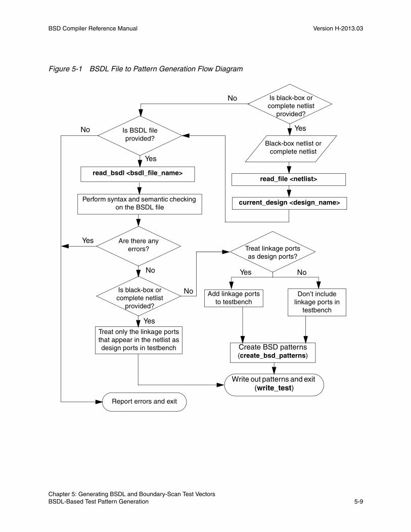
BSD Compiler Reference Manual Version H-2013.03
Figure 5-1 BSDL File to Pattern Generation Flow Diagram
Is black-box or complete netlist
provided?
Black-box netlist or complete netlist
Treat only the linkage ports that appear in the netlist as design ports in testbench
Is BSDL file provided?
Treat linkage ports as design ports?
Are there any errors?
Is black-box or complete netlist
provided?
Add linkage ports to testbench
Don’t include linkage ports in
testbench
Perform syntax and semantic checking on the BSDL file
Report errors and exit
read_bsdl <bsdl_file_name>read_file <netlist>
current_design <design_name>
Create BSD patterns (create_bsd_patterns)
Write out patterns and exit (write_test)
No
No
No
NoNo
Yes
Yes
Yes
Yes
Yes
Chapter 5: Generating BSDL and Boundary-Scan Test Vectors BSDL-Based Test Pattern Generation 5-9Chapter 5: Generating BSDL and Boundary-Scan Test Vectors BSDL-Based Test Pattern Generation 5-9
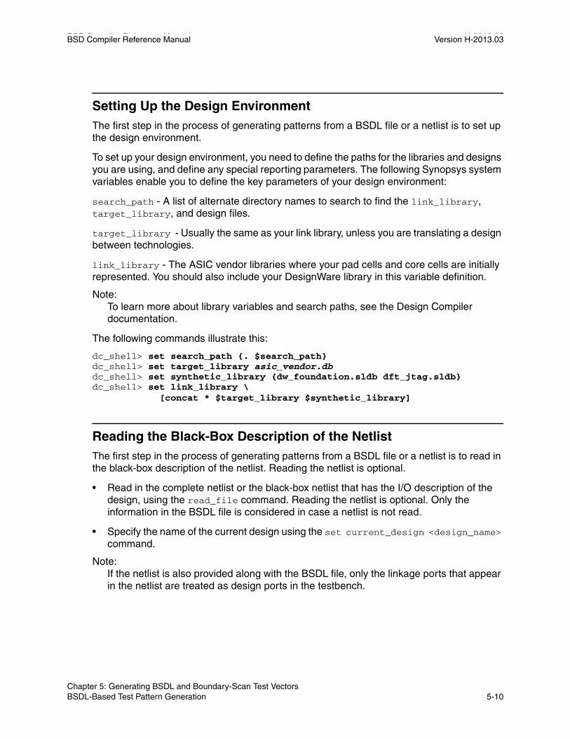
BSD Compiler Reference Manual H-2013.03BSD Compiler Reference Manual Version H-2013.03
Setting Up the Design EnvironmentThe first step in the process of generating patterns from a BSDL file or a netlist is to set up the design environment.
To set up your design environment, you need to define the paths for the libraries and designs you are using, and define any special reporting parameters. The following Synopsys system variables enable you to define the key parameters of your design environment:
search_path - A list of alternate directory names to search to find the link_library, target_library, and design files.
target_library - Usually the same as your link library, unless you are translating a design between technologies.
link_library - The ASIC vendor libraries where your pad cells and core cells are initially represented. You should also include your DesignWare library in this variable definition.
Note: To learn more about library variables and search paths, see the Design Compiler documentation.
The following commands illustrate this:
dc_shell> set search_path {. $search_path}dc_shell> set target_library asic_vendor.dbdc_shell> set synthetic_library {dw_foundation.sldb dft_jtag.sldb}dc_shell> set link_library \ [concat * $target_library $synthetic_library]
Reading the Black-Box Description of the NetlistThe first step in the process of generating patterns from a BSDL file or a netlist is to read in the black-box description of the netlist. Reading the netlist is optional.
• Read in the complete netlist or the black-box netlist that has the I/O description of the design, using the read_file command. Reading the netlist is optional. Only the information in the BSDL file is considered in case a netlist is not read.
• Specify the name of the current design using the set current_design <design_name> command.
Note: If the netlist is also provided along with the BSDL file, only the linkage ports that appear in the netlist are treated as design ports in the testbench.
Chapter 5: Generating BSDL and Boundary-Scan Test Vectors BSDL-Based Test Pattern Generation 5-10

BSD Compiler Reference Manual Version H-2013.03
Reading the BSDL FileRead in the BSDL file using the read_bsdl command. The syntax for the command is as follows.
read_bsdl bsdl_file_name [-add_linkage_as_design_port true | false]
The default for the -add_linkage_as_design_port option is false, which will disregard all the linkage ports during the testbench construction when only the BSDL file is read.
If a netlist is not read in, then the linkage ports may be treated in one of the following two methods:
• If you set the -add_linkage_as_design_port option to true, the linkage ports are listed as design ports in the testbench.
• If you set the -add_linkage_as_design_port option to false, the linkage ports are not listed as design ports in the testbench.
Note: NC ports are treated the same way as linkage ports.
BSD Compiler supports the following BSDL instructions in the BSDL file when reading in the file using the read_bsdl command.
BSD Compiler supports the following cell types in the BSDL file when reading using the read_bsdl command.
Checking for Syntax and Semantic Errors in the BSDL FileBSDL compilation determines if a BSDL description is syntactically correct and makes numerous checks for semantic violations.
EXTEST CLAMP EXTEST_PULSE RUNBIST
BYPASS HIGHZ EXTEST_TRAIN PRELOAD
SAMPLE IDCODE INTEST USERCODE
User-defined instructions
BC_0 BC_2 BC_7 AC_2 AC_SelX
BC_1 BC_4 AC_1 AC_7 AC_SelU
Chapter 5: Generating BSDL and Boundary-Scan Test Vectors BSDL-Based Test Pattern Generation 5-11Chapter 5: Generating BSDL and Boundary-Scan Test Vectors BSDL-Based Test Pattern Generation 5-11

BSD Compiler Reference Manual H-2013.03BSD Compiler Reference Manual Version H-2013.03
The following syntax checks are performed on a BSDL file that is read in using the read_bsdl command:
• Missing punctuation
• Misspelled keywords
• Missing opcodes
• Missing IR capture value
• VHDL and Verilog naming conventions
The following semantic error checks are performed on a BSDL file that is read using the read_bsdl command:
• Omission of required instruction codes (e.g. SAMPLE)
• Missing register associations
• Missing boundary-scan register cells
• Unrecognized attributes in BSDL file that are flagged as warnings
• Unrecognized statements in BSDL file that are flagged as errors
• Incomplete statements that are flagged as errors
• Missing logical or physical port descriptions
• Missing standard package use or COMPONENT_CONFORMANCE statements
• Missing TAP description
• Missing instruction register length or capture value
• Missing mandatory instruction definitions in accordance with IEEE Std 1149.1
• Instructions without Opcodes or Test Data Registers
• Missing boundary-scan register length
• Unrecognized boundary-scan register cell statements
• Unrecognized port names
• Incorrect control cell numbers
If BSD Compiler encounters an error during the syntax or the semantic errors check, it generates an error report and exits.
Chapter 5: Generating BSDL and Boundary-Scan Test Vectors BSDL-Based Test Pattern Generation 5-12
BSD Compiler Reference Manual Version H-2013.03
Some of the errors that are reported are
• Missing BSDL input file. To remedy this error, make sure that the BSDL file is available in the search path and rerun the test.
• Missing I/O netlist. To remedy this error, make sure that the netlist with I/O information is available in the search path and rerun the test.
Any existing User Interface Test messages for BSD Compiler are used as applicable.
Automatic Test Pattern Generation From the BSDL FileIf the syntax and semantic error checks are successful, the BSD patterns are created with the create_bsd_patterns command.
When the BSD patterns are created, they are written out, using the write_test command. These patterns can be simulated using VCS. A lack of mismatches implies that the BSDL file parsing mechanism has generated the correct results. The output BSDL file might differ from the input BSDL file in the sequence of BSDL statements. A BSDL file that is written out using the write_bsdl command is readable using the read_bsdl command.
Note: When the input and the output BSDL files have the same name, the comments in the input file do not appear in the output file.
The create_bsd_patterns and the write_test commands are used as is. There are no modifications to these commands.
Limitations• The following boundary-scan register cell types are not supported: BC_3, BC_5, BC_6,
BC_8, BC_9, BC_10, AC_8, AC_9, and AC_10.
• Not all constructs of the BSDL syntax are supported. For example, user supplied packages are not supported by the BSDL reader.
• User extensions to BSDL as well as the DESIGN_WARNING attribute are not supported.
• The following boundary-scan register cells support INTERNAL function: BC_0, BC_1, BC_2, BC_3, and BC_4.
Chapter 5: Generating BSDL and Boundary-Scan Test Vectors BSDL-Based Test Pattern Generation 5-13Chapter 5: Generating BSDL and Boundary-Scan Test Vectors BSDL-Based Test Pattern Generation 5-13

BSD Compiler Reference Manual H-2013.03BSD Compiler Reference Manual Version H-2013.03
Script Exampleset search_path [list "." ./lib $search_path]set synthetic_library [list dw_foundation.sldb dft_jtag.sldb]set target_library [list class.db]set link_library [concat "*" $target_library $synthetic_library]read_file -format verilog f_bsd.v ;# (optional)current_design testlinkread_bsdl f_bsd.bsdlread_pin_map pin_map.txt #(optional)create_bsd_patternswrite_test -format stil_testbench -output f_stil_tbwrite_test -format verilog -output f_verilog_tbwrite_test -format wgl_serial -output f_wgl_serial
Generating WGL Patterns
You can create WGL patterns using BSD Compiler. Before generating the WGL file, use the read bsd_inserted.ddc command and the check_bsd command to read in the design and check for compliance in your mapped boundary-scan inserted design.
Use the create_bsd_patterns command to capture the WGL patterns in memory. Use the write_test command to generate WGL patterns to disk. The write_test command retrieves the BSD test vectors from memory and writes out the patterns file in WGL format. Using the -format wgl_serial option with the write_test command causes the command to generate a file WGL patterns format.
When executing these commands, BSD Compiler generates the following output in the log file:
write_test -format wgl_serial -output ./pat/f_d1_wgl...Getting test program from design....Writing test patterns to file ./pat/f_d1_wgl.wgl./remote/release/synthesis/A-2007.12-SP2/sparcOS5/syn/ltran/stil2wgl: processing the unnamed PatternExec block// STIL2WGL Version A-2007.12// Copyright (c) 2002-2007 by Synopsys, Inc.// ALL RIGHTS RESERVED//STIL-parse(./pat/f_d1_wgl.wgl.stil): ... STIL version 1.0 ( Design P2001.01) ...STIL-parse(./pat/f_d1_wgl.wgl.stil): ... Building test model ...STIL-parse(./pat/f_d1_wgl.wgl.stil): ... Signals ...
Chapter 5: Generating BSDL and Boundary-Scan Test Vectors Generating WGL Patterns 5-14

BSD Compiler Reference Manual Version H-2013.03
STIL-parse(./pat/f_d1_wgl.wgl.stil): ... SignalGroups ...STIL-parse(./pat/f_d1_wgl.wgl.stil): ... Timing ...STIL-parse(./pat/f_d1_wgl.wgl.stil): ... PatternBurst "_BSD_burst_" ...STIL-parse(./pat/f_d1_wgl.wgl.stil): ... PatternExec ... STIL-parse(./pat/f_d1_wgl.wgl.stil): ... Pattern block "_BSD_block_" ...stil2wgl: End of STIL data; WGL generation complete1
Generating Verilog Testbench
You can specify the name of your Verilog testbench for pattern simulation using the write_test command.
BSD Compiler can generate the Verilog testbench after the insert_dft command and after the check_bsd command using the same command.
For more information about generating a Verilog testbench, refer to the BSD Compiler User Guide.
Generating Manufacturing Test Vectors
The create_bsd_patterns generates five independent sets of test vectors that you can generate separately by using the option -type vectors.
If the TRST* port exists, each set of vectors begins by asynchronously resetting the boundary-scan logic from this port. Because write_bsdl generates the test vectors in this way, each set of vectors can be used and simulated independently.
By default, the generated vectors file contains the five vector sets in consecutive order:
1. Boundary-scan logic reset mechanism test vectors
2. TAP controller transition test vectors
3. Instructions and test data register vectors
4. Boundary-scan register test vectors
5. Leakage failures test vectors
Boundary-Scan Logic Reset Mechanism Test VectorsIn this vector set, the asynchronous reset of your boundary-scan logic TRST* is activated and the state of the TAP controller is checked if the TRST* port exists in your design. Otherwise, it waits for power-up delay and then tests for power-up reset. The synchronous
Chapter 5: Generating BSDL and Boundary-Scan Test Vectors Generating Verilog Testbench 5-15Chapter 5: Generating BSDL and Boundary-Scan Test Vectors Generating Verilog Testbench 5-15
BSD Compiler Reference Manual H-2013.03BSD Compiler Reference Manual Version H-2013.03
reset is also tested by holding the value on the TMS port to logic 1 for five cycles, following the initial reset using TRST* or a PUR cell, which synchronizes the TAP to the Test-Logic-Reset state.
TAP Controller Transition Test VectorsThe TAP controller state machine is tested in this set of vectors. The test is based on the state encoding extracted by compliance checking. Any incorrect transition is detected.
Boundary-Scan Logic Instructions Test VectorsFor each of the instructions defined in the boundary-scan logic, the path from TDI to TDO is tested. For each instruction, one of the test data registers should be selected. The vectors generated depend on the register selected, and every sequence of logic bits should flow transparently from TDI to TDO.
Note: This is the only type of checking performed on the private instructions. For RUNBIST, the behavior of the circuit itself isn’t checked.
For all instructions, BSD Compiler performs a flush test operation through the respective test data registers, checking their functionality.
For the HIGHZ instruction, the state of each output port is checked to ensure it is in a high impedance state.
For the CLAMP instructions, the state of each output port is checked to ensure it is in the state previously loaded in the update stage of the BSR by the SAMPLE and PRELOAD instructions.
For the SAMPLE and PRELOAD instructions, values are applied to the parallel inputs, and the captured values in the shift-register stage are checked.
Boundary-Scan Register Test VectorsUsing the SAMPLE, PRELOAD and EXTEST instructions, the function of the BSR is tested to make sure that each cell can capture values at its primary input and apply values at its primary output.
This set of vectors can be formulated as DC-parametric vectors and controlling by specifying the minimum/maximum input and output ports that can switch simultaneously. See the man pages for bsd_max_in_switching_limit and bsd_max_out_switching_limit.
Chapter 5: Generating BSDL and Boundary-Scan Test Vectors Generating Manufacturing Test Vectors 5-16

BSD Compiler Reference Manual Version H-2013.03
Leakage Failures Test VectorsIf your design contains tristate output drivers, they are set to the high impedance state by using the SAMPLE and PRELOAD instructions. This allows you to check the leakage current resulting from this state.
Creating DC Parametric Test Vectors
You can perform a DC parametric test by creating both leakage vectors and BSR vectors. BSR vectors allow you to test threshold voltage.
If you use the command:
create_bsd_patterns -type leakage
you create vectors to test I/O leakage only.
If you want to ensure that your DC parametric test vectors include both registers and leakage, and can be used to measure threshold voltage and current levels for the I/O, use the command
create_bsd_patterns -type dc_parametric
DC-parametric vectors of the type bsr allow the checking of DC design characteristics such as:
• Input threshold voltage Vil/Vih or current Iil/Iih.
• Output threshold voltage Vol/Voh or current Iol/Ioh.
Checking input threshold voltage or current is done by
1. Applying the logic value 0 on all the functional inputs
2. Capturing that value into the BSR attached to the input ports
3. Shifting out the content of the boundary-scan register
4. Comparing the output stream on the TDO port with the expected value
5. Applying the logic value 1 on all the functional inputs
6. Capturing that value into the BSR attached to the inputs port
7. Shifting out the content of the boundary-scan register
8. Comparing the output stream on the TDO port with the expected value
Chapter 5: Generating BSDL and Boundary-Scan Test Vectors Creating DC Parametric Test Vectors 5-17Chapter 5: Generating BSDL and Boundary-Scan Test Vectors Creating DC Parametric Test Vectors 5-17

BSD Compiler Reference Manual H-2013.03BSD Compiler Reference Manual Version H-2013.03
Checking output threshold voltage or current is done by
1. Shifting a stream of bits into the boundary-scan register that sets all the registers attached to the output port to a logic 0
2. Updating the value shifted into the update stage of the BSR.
3. Strobing all the functional outputs of the design
4. Comparing to logic 0
5. Shifting into the boundary-scan register a stream of bits setting all the BSR attached to the output port to logic 1
6. Updating the value shifted into the update stage of the BSR
7. Strobing all the functional outputs of the design
8. Comparing to logic 1
Setting Input Switching LimitsThe bsd_max_in_switching_limit variable specifies the number of inputs to be switched together. By default, all inputs are switched together, but this can cause ground bounce. When the bsd_max_in_switching_limit variable is set, only the specified number of ports change values while the others remain at their existing logic value. The cycle repeats until all the inputs go from X to 0 and then from 0 to 1. For example, when you set this variable to 8, only 8 ports change input values.
dc_shell> set_app_var bsd_max_in_switching_limit 8
Setting Output Switching LimitsThe bsd_max_out_switching_limit variable specifies the number of outputs to be switched together. By default, all outputs are switched together, but this can cause ground bounce. When the bsd_max_out_switching_limit variable is set, only the specified number of ports change values while the others remain at their existing logic values. The cycle repeats until all the outputs go from X to 0 and then from 0 to 1. For example, when you set this variable to 8, only 8 ports change output values.
dc_shell> set_app_var bsd_max_out_switching_limit 8
Chapter 5: Generating BSDL and Boundary-Scan Test Vectors Creating DC Parametric Test Vectors 5-18

Index
Aanalyzing
bypass register 4-24output signals 4-47PRELOAD instruction 4-46SAMPLE instruction 4-46signatures 4-41system inputs 4-47test data output 4-11transparency 4-47
area overhead,control BSR cells and 2-65asynchronous BC_1 cell type interface 2-20asynchronous BC_2 cell type interface 2-21asynchronous BC_4 cell type interface 2-23asynchronous BC_7 cell type interface 2-24asynchronous boundary-scan design
interface 2-50asynchronous implementation 2-14, 2-15asynchronous reset 2-11asynchronous reset, failure 4-15attributes
setting on differential I/O pad cells 2-4setting on pad cells 2-3
BBC_1 cell
data BSR cell 2-39inserting 2-37
BC_2 cellcontrol BSR cell 2-39inserting 2-34
BC_4 cell, inserting 2-36BC_7 cell, data BSR cell 2-39bidirectional port
boundary-scan register cells 1-33cell insertion 2-39degenerated 2-33
bidirectional port cell types 2-45binary code
BYPASS instruction 2-49EXTEST instruction 2-49IDCODE instruction 2-49instructions 2-49PRELOAD instruction 2-49SAMPLE instruction 2-49
binary encoding, instruction register length and 2-48
BIST, requirements 1-34black box, design ports and 2-10black boxes, linkage ports and 2-11board test
existence test 1-8infrastructure test 1-7interconnect test 1-8
IN-1 IN-1

BSD Compiler Reference Manual Version H-2013.03
board test strategy 1-7board-level, boundary scan at the 1-5boundary-scan
at board-level 1-5choosing components 2-18core interface and 1-35custom components 2-18design flow
BSDL generation 1-36compliance checking 1-36
in overall design flow 1-34interface components 2-18requirements, design flow 1-35scan path 1-5
boundary-scan cell type specificationeffect of 2-43
boundary-scan components, fundamental 1-2boundary-scan design
register cells 2-62boundary-scan keywords 5-3boundary-scan logic
unmapped 2-61boundary-scan register
cannot update 4-28described 1-26extracting information from 4-25extracting shift register stage 4-21extracting update register stage 4-21functionality 1-27IEEE Std 1149.1 architecture 1-8label fields 5-4selecting 1-27signatures 4-41updates during CLAMP instruction 4-49updates incorrectly on rising edge of TCK
4-35boundary-scan register cell
analyzing structure 4-55and INTEST instruction 4-51assigning cell types to 4-46basic functionality 1-3bidirectional 1-33
capture descriptors 4-56characterizing behavior 4-47control cells and area overhead 2-65correspondence with associated ports 4-26creating 1-32described 1-28differentiating 4-55driven by inactive element 4-28fails to drive design port 4-49fanin and 1-32fanout and 1-32feed-through connections and 2-62fundamental, description 1-2identifying 4-21illegal capture descriptors 4-56improperly placed on compliance port 4-37improperly placed on TAP port 4-36invalid type 4-55logic not allowed 4-37merged improperly 4-37, 4-38merged unnecessarily 4-37missing on design input port 4-36missing on design output port 4-36multiple cells driving pads 4-37no primary input found 4-44no primary output found 4-45not driven by INTEST instruction 4-50parallel mode 1-3path delay and 2-63primary input 1-2primary input not found 4-54primary output 1-2removal of 2-64substitution 2-64tristate output drivers and 2-62tristate outputs 1-33undetected
BSR cell update stage flop 4-39missing control BSR 4-38
unpropagated datainput cell 4-38output cell 4-38, 4-53
IN-2 Index IN-2
BSD Compiler Reference Manual Version H-2013.03
BSDLgeneration, boundary-scan design flow and
1-36providing INTEST information for 5-6reserved words 5-2using check_bsd before generating 4-2
BSRdescribed 1-26functionality 1-27
BSR cell 2-6bidirectional 1-33creating 1-32described 1-28fanin and 1-32fanout and 1-32grouping 2-42three-state outputs 1-33
BSR cell routingdefault 2-45port-to-pin mapping file and 2-45
BSR cells, linkage ports and 2-11BSR embedded pad cells 2-6BYPASS instruction
binary code for 2-49mandated by IEEE Std 1149.1 1-12
bypass registeranalyzing 4-24extracting shift register stage 4-20function 1-24IEEE Std 1149.1 architecture 1-8not selected by all-1s opcode 4-33shift register stage value 4-33
Ccapture clock signal 2-31capture descriptor
invalid 4-47invalid number 4-54
capture enable signal 2-31capture operation, described 1-3, 1-6
causes of manufacturing defects 1-7cell types
bidirectional port 2-45control port 2-44input port 2-43output port 2-44tristate output port 2-44
characterizing opcodes 4-41check_bsd command
as BSDL preprocessor 4-2as stand-alone 4-2as test vector preprocessor 4-2checks performed by 4-8implementation 4-2preparation 4-5purpose 4-2with write_bsdl 5-2
checkingphase four tasks 4-46phase one tasks 4-9phase three tasks 4-39phase two tasks 4-20pull-ups 4-11TAP controller behavior 4-10TCK halt states 4-11
CLAMP instructionallowed by IEEE Std 1149.1 1-13BSR cell fails to drive design port during 4-49BSR updates during 4-49inferred 4-42output conditioning 4-42
clocks, inferring 4-21commands
check_bsdas BSDL preprocessor 4-2as stand-alone 4-2as test vector preprocessor 4-2checks performed by 4-8implementation 4-2preparation 4-5purpose 4-2with write_bsdl 5-2
IN-3 Index IN-3
BSD Compiler Reference Manual Version H-2013.03
create_bsd_patterns, using check_bsd with 4-2
define_dft_design 2-18group 2-42insert_dft
BC_1 cells 2-37BC_2 cells 2-34BC_4 cells 2-36black box design ports and 2-10global enables and 2-33mandatory design elements 2-3nonmandatory design elements 2-3tristate output drivers and 2-33
preview_dft 2-62reset_bsd_specification 5-6, 5-7set_attribute 2-4set_bsd_compliance 4-7set_bsd_configuration -asynchronous_reset
2-12, 2-14set_bsd_configuration -style 2-14set_bsd_instruction 5-5, 5-6set_bsd_instruction -internal_scan 2-58set_bsd_linkage_port 2-11set_bsd_power_up_reset 2-13set_dft_signal 2-12set_max_delay 2-65set_message_severity 4-3set_scan_path 2-45ungroup 2-42write_bsdl
compliance checking 5-2naming_check option 5-2
compliance checkingboundary-scan design flow and 1-36in write_bsdl 5-2linkage ports and 2-11phase four tasks 4-46phase one tasks 4-9phase three tasks 4-39phase two tasks 4-20phases 4-9
compliance-enable patterns 4-57
compliance-enable portsboundary-scan register cell improperly
placed on 4-37failure to specify 4-13
control BSR celland area overhead 2-65BC_2 2-39
control port behavior, checking 4-10control port cell types 2-44control signal, selecting 2-55control signals, described 1-18controlling BSDL line length 5-3create_bsd_patterns command, using
check_bsd with 4-2critical path
BSR cell removal and 2-64cell substitution and 2-64output 2-65
custom designasynchronous TAP controller 2-31synchronous TAP controller 2-31TAP controller 2-25
Ddata BSR cell
BC_1 2-39BC_7 2-39
data inversionat particular cell 4-28at test data out 4-27
decoding logic for instructions 2-50decoding pins, extracting 4-40decoding the instruction register 1-14default BSR cell routing order 2-45define_dft_design command 2-18definition
error messages 4-3information messages 4-2warning messages 4-2
degenerated bidirectional ports 2-33
IN-4 Index IN-4

BSD Compiler Reference Manual Version H-2013.03
descriptioncapture operation 1-3, 1-6check_bsd command 4-2external testing 1-7EXTEST 1-7instruction register 1-10internal testing 1-7INTEST instruction 1-7intolerable violations 4-4parallel-load operation 1-3parallel-unload operation 1-4run-test-idle state 1-20select_IR_scan state 1-20serial-mode operation 1-4serial-mode signals 1-4shift-in operation 1-6shift-out operation 1-6TAP controller design 2-47test-logic-reset state 1-19tolerable violations 4-4update operation 1-4, 1-6update_IR state 1-21
design elementsmandatory 2-3nonmandatory 2-3
design elements, verifying 4-46design flow, boundary-scan 1-35design input port, missing boundary-scan
register cells on 4-36design output port, missing boundary-scan
register cells on 4-36design port, logic not allowed 4-37design synthesis 2-42DesignWare Foundation Library
BC_1 BSR cell 2-37BC_2 BSR cells 2-34BC_4 BSR cell 2-36DW_tap_uc 2-47
device identification registerextracting information from 4-24extracting shift register stage 4-20
not connected 4-33device number 1-26differential I/O pad cells, setting attributes on
2-4DW_tap_uc, default TAP controller 2-25, 2-29,
2-47DW_tap_uc, DesignWare element 2-47DW_tap, setting 2-25
Eembedded in pads 2-6embedded pad cells 2-6enable signals, vendor requirements 4-6environment variables
systemlink_library 5-10search_path 5-10target_library 5-10
error messagesdefined 4-3implications 4-3
errors, downgrading to warning 4-3errors, state machine
black box pad cells 4-13sources 4-13
example of port ordering 2-45existence test, board-level 1-8exit state 1-23Exit2 state 1-24external testing, described 1-7EXTEST instruction
binary code for 2-49described 1-7mandated by IEEE Std 1149.1 1-12output conditioning and 4-52output not driven during 4-53
extractingboundary-scan shift register stage 4-21boundary-scan update register stage 4-21bypass register shift register stage 4-20
IN-5 Index IN-5

BSD Compiler Reference Manual Version H-2013.03
decoding pins 4-40device identification register shift register
stage 4-20sequential cells 4-10shift register stage 4-20
extractionboundary-scan register information 4-25bypass register information 4-24device identification register information 4-24instruction register shift cells 4-23register information 4-22shift register update stage 4-23state encoding 4-11TAP controller logic 4-10TAP controller state cells 4-10
Ffanin, boundary-scan register cells and 1-32fanout, boundary-scan register cells and 1-32feed-through connections, boundary-scan
register cells and 2-62feedthroughs, searching for 4-42finite state machine
described 1-19state table, described 1-19
flip-flops, insufficient number found 4-12function of
instruction register 1-10TAP controller with instruction register 1-10
Ggenerating boundary-scan register test vectors
5-16generating instructions test vectors 5-16generating leakage failures test vectors 5-17generating manufacturing test vectors 5-15generating reset mechanism test vectors 5-15generating TAP controller transition test
vectors 5-16
Generating Verilog DPVusing BSD Compiler 5-7
global enables, insert_dft and 2-33ground bounce, avoiding 2-65grouping BSR cells 2-42
Hhalt states, checking 4-11hierarchy, grouping BSR cells 2-42HIGHZ instruction
allowed by IEEE Std 1149.1 1-14inferred 4-42output conditioning 4-42
IIDCODE instruction
allowed by IEEE Std 1149.1 1-13binary code for 2-49inferred 4-43
identification registerdescription 1-25device number 1-26IEEE Std 1149.1 architecture 1-8incorrect length 4-34incorrect LSB value 4-34incorrect manufacturer code 4-34manufacturer code 1-26part number 1-26
identifying primary inputs 4-42identifying primary outputs 4-42IEEE Std 1149.1
architectureactive registers in 1-9boundary-scan register 1-8bypass register 1-8elements 1-8identification register 1-8instruction register 1-8TAP 1-8
IN-6 Index IN-6

BSD Compiler Reference Manual Version H-2013.03
TAP controller 1-8mandatory instructions
BYPASS 1-12described 1-12EXTEST 1-12PRELOAD 1-13SAMPLE 1-12
optional instructionsCLAMP 1-13HIGHZ 1-14IDCODE 1-13INTEST 1-13RUNBIST 1-13
IEEE Std 1149.6AC cell mode controls 3-7AC pin driver structure 3-8AC/DC selection cell AC_SelU 3-4AC/DC selection cell AC_SelX 3-3BIDI output cell AC_7 3-6boundary-scan components 3-2EXTEST_PULSE 3-14EXTEST_TRAIN 3-13output data cell AC_1 3-5output data cell AC_2 3-5overview 3-2test receiver with BSR cells 3-9
implementationasynchronous 2-14, 2-15synchronous 2-14, 2-16
implementing private opcodes 1-14inactive element driving cell 4-28incorrect least significant bit in instruction
register 4-31inferring clocks 4-21inferring instructions
CLAMP 4-42HIGHZ 4-42IDCODE 4-43INTEST 4-42RUNBIST 4-43USERCODE 4-43
inferring primary inputs 4-43inferring primary outputs 4-43information messages
defined 4-2implications 4-2
infrastructure test, board-level 1-7initialization
checking TAP controller 4-10inconsistent states 4-16incorrect 4-15messages 4-13no register found during 4-32undefined 4-16
input port cell types 2-43inputs, analyzing system 4-47insert_dft command
BC_1 cells 2-37BC_2 BSR cells 2-34BC_4 cells 2-36black box design ports and 2-10global enables and 2-33mandatory design elements for 2-3nonmandatory design elements for 2-3tristate output drivers and 2-33
instructionBYPASS, does not initialize 4-32CLAMP
BSR cell fails to drive design port 4-49BSR updates during 4-49
decoding logic for 2-50EXTEST
output conditioning and 4-52output not driven during 4-53
IDCODE does not initialize 4-32incorrect during test-logic-reset 4-33INTEST
clock boundary-scan register cell and 4-51does not drive boundary-scan register cell
4-50opcodes 4-42searching for 4-42
mandatory
IN-7 Index IN-7

BSD Compiler Reference Manual Version H-2013.03
BYPASS 1-12EXTEST 1-12PRELOAD 1-13SAMPLE 1-12
optionalCLAMP 1-13HIGHZ 1-14IDCODE 1-13INTEST 1-13RUNBIST 1-13
output conditioning 4-41PRELOAD
analyzing 4-46inferring 4-41opcodes corresponding to 4-41
PRELOAD, using 2-49RUNBIST, output fails to retain state 4-51SAMPLE
analyzing 4-46inferring 4-41opcodes corresponding to 4-41
SAMPLE, using 2-49SAMPLE/PRELOAD
cannot capture data 4-44not found 4-44
instruction registerand TAP controller, function 1-10decoding 1-14defined 1-10extracting shift cells 4-23extracting shift register stage 4-20function 1-10in capture mode, mandatory pattern 1-10incorrect least significant bit 4-31initialization
BYPASS instruction 4-32IDCODE instruction 4-32
lengthbinary encoding style 2-48one-hot encoding style 2-48
length of 2-48loading 1-14
minimum length requirement 1-10not inferred 4-31setting length of 2-49shifts on wrong clock edge 4-32updates on wrong clock edge 4-31, 4-32using 1-14
instructionsaccess internal register using RUNBIST 1-34binary codes for 2-49implementing 2-48INTEST, providing BSDL information for 5-6mandated by IEEE Std 1149.1 1-12private 1-33private, implementing 2-48
interconnect test, board-level 1-8interconnect testing 1-7interface
asynchronous BC_1 cell type 2-20asynchronous BC_2 cell type 2-21asynchronous BC_4 cell type 2-23asynchronous BC_7 cell type 2-24asynchronous boundary-scan design 2-50synchronous BC_1 cell type 2-19synchronous BC_2 cell type 2-21synchronous BC_4 cell type 2-22synchronous BC_7 cell type 2-24synchronous boundary-scan design 2-51
interface requirements, boundary-scan component 2-18
interface, boundary-scan and core 1-35internal scan
accessing through boundary-scan logic 2-57accessing through top-level ports 2-58
internal scan chains, creating 2-59internal testing, described 1-7INTEST instruction
allowed by IEEE Std 1149.1 1-13clock boundary-scan register cell 4-51described 1-7does not drive boundary-scan register cell
4-50
IN-8 Index IN-8

BSD Compiler Reference Manual Version H-2013.03
inferred 4-42opcodes 4-42providing BSDL information for 5-6searching for 4-42
intolerable violations, described 4-4invalid capture descriptor 4-47invalid state transition 4-14invalid state transition synchronous reset
sequence 4-14inversion, data
at particular cell 4-28at test data out 4-27
JJETAG 1-2Joint Test Action Group 1-2JTAG 1-2
Kkeywords, boundary scan 5-3
Lline length, controlling BSDL 5-3link_library system variable 5-10linkage ports 2-11loading instruction register 1-14logic required for mode signal generation 2-60
Mmandatory design elements 2-3mandatory instructions
BYPASS, described 1-12described 1-12EXTEST, described 1-12PRELOAD, described 1-13SAMPLE, described 1-12
manufacturer code 1-26manufacturer code, incorrect value 4-34manufacturing defects
causes of 1-7on periphery 1-7testing for 1-7
manufacturing test vectorsboundary-scan register test vectors 5-16generating 5-15instructions test vectors 5-16leakage failures test vectors 5-17reset mechanism vectors 5-15TAP controller transition vectors 5-16
mergingimproper 4-37, 4-38unnecessary 4-37
merging boundary-scan register cells 2-62messages
errordefined 4-3implications 4-3
informationdefined 4-2implications 4-2
initialization 4-13reset 4-13state transition, invalid 4-14TEST-1110 4-27, 4-29TEST-1110a 4-27, 4-29TEST-1111 4-27, 4-29TEST-1112 4-27, 4-30TEST-1113 4-27, 4-30TEST-1114 4-27, 4-30TEST-1115 4-27, 4-30TEST-1121 4-36, 4-38TEST-1122 4-36, 4-38TEST-1123 4-36, 4-38, 4-53TEST-1124 4-36, 4-38TEST-1125 4-36, 4-39TEST-1128 4-52TEST-1129 4-54, 4-56TEST-1129a 4-54, 4-56
IN-9 Index IN-9

BSD Compiler Reference Manual Version H-2013.03
TEST-1130 4-54, 4-56TEST-1131 4-54, 4-56TEST-1133 4-49, 4-50TEST-1136 4-49, 4-50TEST-801 4-3TEST-802 4-3TEST-811 4-12TEST-812 4-12TEST-813 4-12TEST-814 4-13, 4-14, 4-16TEST-816 4-13, 4-14TEST-816a 4-13, 4-15TEST-816b 4-14, 4-15TEST-817 4-17TEST-818 4-17TEST-819 4-19, 4-20TEST-820 4-52TEST-821 4-17, 4-18TEST-822 4-14, 4-15TEST-823 4-14, 4-15TEST-824 4-27, 4-28TEST-824a 4-27TEST-824b 4-27, 4-28TEST-825 4-30, 4-31TEST-826 4-30, 4-31TEST-828 4-30, 4-31TEST-829 4-34TEST-830a 4-32, 4-33TEST-832 4-32, 4-33TEST-835 4-34TEST-836 4-34TEST-837 4-43, 4-44TEST-838 4-35, 4-36TEST-838a 4-35, 4-36TEST-839 4-35, 4-36TEST-840 4-35, 4-37TEST-841 4-43, 4-44TEST-843 4-35, 4-37TEST-844 4-31TEST-845 4-57TEST-846 4-35TEST-847 4-49
TEST-849 4-35, 4-37TEST-850 4-14, 4-16TEST-850a 4-14, 4-16TEST-851 4-31TEST-854 4-27, 4-28TEST-855 4-27, 4-28TEST-856 4-27, 4-28TEST-858 4-31, 4-32TEST-860 4-35, 4-37TEST-860a 4-36, 4-37TEST-861 4-27, 4-28TEST-864 4-27, 4-29TEST-865 4-27, 4-29TEST-870 4-48TEST-871 4-47TEST-872 4-52TEST-873 4-52TEST-874 4-49TEST-875 4-43, 4-44TEST-876 4-52, 4-53TEST-877 4-53TEST-878 4-53, 4-54TEST-880 4-32, 4-33TEST-881 4-32, 4-33TEST-882 4-54TEST-883 4-19, 4-20TEST-884 4-19, 4-20TEST-886 4-50, 4-51TEST-887 4-50, 4-51TEST-889 4-54, 4-55TEST-890 4-43, 4-44TEST-891 4-43, 4-45TEST-896 4-43, 4-45TEST-897 4-43, 4-45TEST-898 4-54, 4-55warning
defined 4-2implications 4-3
missinginstruction register 4-31pull-up 4-19test access ports 4-12
IN-10 Index IN-10

BSD Compiler Reference Manual Version H-2013.03
missing tap ports 2-10mode signal generation, logic required for 2-60multiple violations 4-3
Nnames, checking for reserved words 5-2non-digital ports 2-43nonmandatory design elements 2-3
Oone-hot encoding, instruction register length
and 2-48opcodes
all-1s does not select bypass register 4-33associating signatures with 4-41characterizing 4-41does not select any register 4-44INTEST 4-42PRELOAD 4-41private, implementing 1-14SAMPLE 4-41undefined 1-14
optimization techniques 2-62optional instructions
CLAMP, described 1-13HIGHZ, described 1-14IDCODE, described 1-13INTEST, described 1-13RUNBIST, described 1-13
outputanalyzing signal 4-47fails to retain state 4-51not driven during EXTEST 4-53not driven properly 4-53
output conditioningCLAMP instruction 4-42EXTEST instruction and 4-52HIGHZ 4-42signature classification and 4-41
output port cell types 2-44
Ppad cell
BSR embedded in pad 2-6pad cells
linkage ports and 2-11setting attributes on 2-3synthesizing 2-42
parallel modeboundary-scan cells 1-3illustrated 1-5
parallel-load operation, described 1-3parallel-unload operation, described 1-4part number 1-26path delay, boundary-scan register cells and
2-63path, transparent 4-25pause state 1-23periphery, manufacturing defects on 1-7port ordering, example 2-45ports
compliance-enableboundary-scan register cell improperly
placed on 4-37failure to specify 4-13
correspondence with associated boundary-scan register cells 4-26
missing boundary-scan register cellson input 4-36on output 4-36
non-digital 2-43port-to-pin mapping file, using 2-45power-up reset 2-11, 2-13power-up reset failure 4-15power-up, mandated state for 1-23predicting timing impact 2-51PRELOAD instruction
analyzing 4-46binary code for 2-49
IN-11 Index IN-11

BSD Compiler Reference Manual Version H-2013.03
mandated by IEEE Std 1149.1 1-13using 2-49
preview_dft command 2-62primary inputs
boundary-scan cells on 1-2identifying 4-42inferring 4-43not found 4-54not found on cell 4-44
primary outputsboundary-scan cells on 1-2identifying 4-42inferring 4-43not found on cell 4-45
private instructions 1-33, 2-48private instructions, implementing 2-48private opcodes, implementing 1-14pull-ups
checking for 4-11missing 4-19
Rregister
active in IEEE Std 1149.1 architecture 1-9all-1s selects multibit register 4-33boundary-scan
extracting information from 4-25updates incorrectly on rising edge of TCK
4-35bypass, not selected by all-1s 4-33checking shifting structure for 4-20device identification
extracting information from 4-24not connected 4-33
extracting information from 4-22identification
incorrect length 4-34incorrect LSB value 4-34incorrect manufacturer code 4-34
none selected by opcode 4-44register cells, merging 2-62
register length, instruction register 1-10registers
boundary-scandescribed 1-26functionality 1-27selecting 1-27
bypass, description 1-24identification
description 1-25device number 1-26manufacturer code 1-26part number 1-26
instructionbinary encoding style and 2-48one-hot encoding style and 2-48
requirements, BIST 1-34requirements, test data register 2-50reserved words
BSDL 5-2checking for 5-2VHDL 5-2
resetmessages 4-13power-up failure 4-15TRST fails 4-14verifying mechanisms 4-11
reset_bsd_specification command 5-6, 5-7routing order, set_scan_path command and
2-45RUNBIST instruction 1-34
allowed by IEEE Std 1149.1 1-13inferred 4-43output fails to retain state 4-51specifying 5-5
run-test-idle state, described 1-20
SSAMPLE instruction
analyzing 4-46binary code for 2-49
IN-12 Index IN-12

BSD Compiler Reference Manual Version H-2013.03
mandated by IEEE Std 1149.1 1-12using 2-49
SAMPLE/PRELOAD instructioncannot capture data 4-44not found 4-44
scan path, boundary scan 1-5scan-enable signal 2-51scan-through-TAP, using 2-59search_path system variable 5-10select_IR_scan state, described 1-20selecting control signals 2-55sentinel_val pins 2-29sequential cells, extracting 4-10serial mode
illustrated 1-5operation, described 1-4signals, described 1-4
set_attribute command 2-4set_bsd_compliance command 4-7set_bsd_configuration -asynchronous_reset
command 2-12, 2-14set_bsd_configuration -style command 2-14set_bsd_instruction command 5-5, 5-6set_bsd_instruction -internal_scan 2-58set_bsd_linkage_port command 2-11set_bsd_power_up_reset command 2-13set_dft_signal command 2-12set_max_delay command 2-65set_message_severity command 4-3set_scan_path command 2-45setting differential I/O pad cell attributes 2-4setting pad cell attributes 2-3shift cells, extracting 4-23shift register
extracting the update stage 4-23verifying capture data 4-23verifying size 4-23
shift register stageextracting 4-20
extracting boundary-scan register’s 4-21extracting bypass register’s 4-20extracting device identification register’s 4-20
shift-enable signal 2-51shift-in operation, described 1-6shifting structure, checking 4-20shift-out operation, described 1-6signal not driven by external source 4-52signatures
analyzing 4-41associating opcodes with 4-41boundary-scan register 4-41
soft macro pad cells 2-5state
invalid transition 4-20TAP controller fails to retain 4-20
state encoding, extracting 4-11state flip-flops, insufficient number found 4-12state machine errors
black box pad cells 4-13common sources 4-13
state table operationsmandatory power-up state 1-23run-test-idle 1-20select_IR_scan 1-20test-logic-reset 1-19update_IR 1-21
state transitioninvalid 4-14messages, invalid 4-14
statesexit 1-23Exit2 1-24pause 1-23
strategy, board-test 1-7substitution
control-only cells 2-64synchronizing
behavior, incorrect 4-15sequence, invalid state transition and 4-14
synchronous BC_1 cell type interface 2-19
IN-13 Index IN-13

BSD Compiler Reference Manual Version H-2013.03
synchronous BC_2 cell type interface 2-21synchronous BC_4 cell type interface 2-22synchronous BC_7 cell type interface 2-24synchronous boundary-scan design, interface
2-51synchronous implementation 2-14, 2-16synchronous reset 2-11synchronous reset, invalid 4-15synthesis 2-42synthesizing pad cells 2-42system input, improperly resets TAP 4-15system variables
link_library 5-10search_path 5-10target_library 5-10
TTAP controller
behavior, checking 4-10design description 2-47DW_tap 2-25DW_tap_uc pins 2-27DW_tap_uc, default 2-25extracting state cells 4-10extracting state encoding 4-11fails to retain state 4-20failure to reset 4-14IEEE Std 1149.1 architecture 1-8improper initialization 4-15incorrect synchronizing behavior 4-15initialization, checking 4-10initialized states do not exist 4-16initialized states inconsistent 4-16interface diagram 2-25invalid state transition 4-20logic requirements 1-24logic, extracting 4-10
TAP Controller, initialization 2-11TAP controller, initializing, using power-up
reset 2-13
TAP Controller, initializing, using TRST 2-12, 2-14
TAP portboundary-scan register cells placed
improperly on 4-36extracting TAP controller state cells 4-10missing 4-12none defined 4-12not inactive 4-48verifying 4-10
tap ports, missing 2-10target_library system variable 5-10TCK halt states, checking 4-11test access port
boundary-scan register cell improperly placed on 4-36
IEEE Std 1149.1 architecture 1-8missing 4-12none defined 4-12not inactive 4-48
test clockinstruction register shifting on wrong edge
4-32instruction register updating on wrong edge
4-31, 4-32rising edge and bypass register 4-33
test data outchanges on incorrect clock edge 4-18incorrectly active 4-17incorrectly inactive 4-17not driven 4-28port driven by constant source 4-29port not enabled 4-28port not enabled during shift-dr 4-29
test data output, analyzing conditioning 4-11test data register
requirements 2-50update mechanism 2-51
test protocol, internal scan 2-59test reset fails to reset TAP 4-14test vectors, generating 5-15
IN-14 Index IN-14
BSD Compiler Reference Manual Version H-2013.03
test_bsdl_max_line_length variable 5-3TEST-1110 message 4-27, 4-29TEST-1110a message 4-27, 4-29TEST-1111 message 4-27, 4-29TEST-1112 message 4-27, 4-30TEST-1113 message 4-27, 4-30TEST-1114 message 4-27, 4-30TEST-1115 message 4-27, 4-30TEST-1121 message 4-36, 4-38TEST-1122 message 4-36, 4-38TEST-1123 message 4-36, 4-38, 4-53TEST-1124 message 4-36, 4-38TEST-1125 message 4-36, 4-39TEST-1128 message 4-52TEST-1129 message 4-54, 4-56TEST-1129a message 4-54, 4-56TEST-1130 message 4-54, 4-56TEST-1131 message 4-54, 4-56TEST-1133 message 4-49, 4-50TEST-1136 message 4-49, 4-50TEST-801 message 4-3TEST-802 message 4-3TEST-811 message 4-12TEST-812 message 4-12TEST-813 message 4-12TEST-814 message 4-13, 4-14, 4-16TEST-816 message 4-13, 4-14TEST-816a message 4-13, 4-15TEST-816b message 4-14, 4-15TEST-817 message 4-17TEST-818 message 4-17TEST-819 message 4-19, 4-20TEST-820 4-17TEST-820 message 4-52TEST-821 message 4-17, 4-18TEST-822 message 4-14, 4-15TEST-823 message 4-14, 4-15TEST-824 message 4-27, 4-28
TEST-824a message 4-27TEST-824b message 4-27, 4-28TEST-825 message 4-30, 4-31TEST-826 message 4-30, 4-31TEST-828 message 4-30, 4-31TEST-829 message 4-34TEST-830a message 4-32, 4-33TEST-832 message 4-32, 4-33TEST-835 message 4-34TEST-836 message 4-34TEST-837 message 4-43, 4-44TEST-838 message 4-35, 4-36TEST-838a message 4-35, 4-36TEST-839 message 4-35, 4-36TEST-840 message 4-35, 4-37TEST-841 message 4-43, 4-44TEST-843 message 4-35, 4-37TEST-844 message 4-31TEST-845 message 4-57TEST-846 message 4-35TEST-847 message 4-49TEST-849 message 4-35, 4-37TEST-850 message 4-14, 4-16TEST-850a message 4-14, 4-16TEST-851 message 4-31TEST-854 message 4-27, 4-28TEST-855 message 4-27, 4-28TEST-856 message 4-27, 4-28TEST-858 message 4-31, 4-32TEST-860 message 4-35, 4-37TEST-860a message 4-36, 4-37TEST-861 message 4-27, 4-28TEST-864 message 4-27, 4-29TEST-865 message 4-27, 4-29TEST-870 message 4-48TEST-871 message 4-47TEST-872 message 4-52TEST-873 message 4-52
IN-15 Index IN-15

BSD Compiler Reference Manual Version H-2013.03
TEST-874 message 4-49TEST-875 message 4-43, 4-44TEST-876 message 4-52, 4-53TEST-877 message 4-53TEST-878 message 4-53, 4-54TEST-880 message 4-32, 4-33TEST-881 message 4-32, 4-33TEST-882 message 4-54TEST-883 message 4-19, 4-20TEST-884 message 4-19, 4-20TEST-886 message 4-50, 4-51TEST-887 message 4-50, 4-51TEST-889 message 4-54, 4-55TEST-890 message 4-43, 4-44TEST-891 message 4-43, 4-45TEST-896 message 4-43, 4-45TEST-897 message 4-43, 4-45TEST-898 message 4-54, 4-55test-logic-reset
incorrect instruction loaded during 4-33power-up state 1-23state, described 1-19
testsinterconnect 1-7manufacturing defects 1-7
timing impact, mitigating by cell substitution 2-64
timing, impact predictability 2-51tolerable violations, described 4-4top-level ports, accessing internal scan
through 2-58transitions, checking TAP controller state 4-10transparency, analyzing 4-47transparent path 4-25tristate output drivers, boundary-scan register
cells and 2-62tristate output port cell types 2-44tristate output, insert_dft and 2-33
tristate outputs, boundary-scan register cells 1-33
tristate, multiple boundary-scan register cells drive 4-37
TRSTfails asynchronous reset 4-15fails to reset TAP controller 4-14
Uunmapped boundary-scan logic 2-61update mechanism 2-51update operation, described 1-4, 1-6update register stage
extracting boundary-scan register’s 4-21extracting shift register 4-23
update_IR state, described 1-21USERCODE, inferred instruction 4-43
Vvariables
bsd_use_old_tap 2-25system
link_library 5-10search_path 5-10target_library 5-10
test_bsdl_max_line_length 5-3vendor enable-signal requirements 4-6verification
phase four tasks 4-46phase one tasks 4-9phase two tasks 4-21phases 4-9reset mechanisms 4-11shift register capture data 4-23shift register size 4-23TAP ports 4-10
verifying design elements 4-46VHDL reserved words 5-2violations
IN-16 Index IN-16

BSD Compiler Reference Manual Version H-2013.03
intolerable, described 4-4multiple 4-3tolerable, described 4-4
Wwarning messages
defined 4-2implications 4-3
write_bsdl commandcompliance checking 5-2naming_check option 5-2
IN-17 Index IN-17