chapter 10 cvd and dielectric thin film - miun.se
TRANSCRIPT

Hong Xiao, Ph. D. www2.austin.cc.tx.us/HongXiao/Book.htm 1
Chapter 10CVD and Dielectric
Thin FilmHong Xiao, Ph. D.
www2.austin.cc.tx.us/HongXiao/Book.htm

Hong Xiao, Ph. D. www2.austin.cc.tx.us/HongXiao/Book.htm 2
Objectives
• Identify at least four CVD applications
• Describe CVD process sequence
• List the two deposition regimes anddescribe their relation to temperature
• List two dielectric thin films
• Name the two most commonly used siliconprecursors for dielectric CVD

Hong Xiao, Ph. D. www2.austin.cc.tx.us/HongXiao/Book.htm 3
CVD Oxide vs. Grown Oxide
Grown film Deposited filmBare silicon
SiO2
SiO2
SiSi Si

Hong Xiao, Ph. D. www2.austin.cc.tx.us/HongXiao/Book.htm 4
CVD Oxide vs. Grown Oxide
Grow
• Oxygen is from gasphase
• Silicon from substrate
• Oxide grow intosilicon
• Higher quality
CVD
• Both oxygen andsilicon are from gasphase
• Deposit on substratesurface
• Lower temperature
• Higher growth rate

Hong Xiao, Ph. D. www2.austin.cc.tx.us/HongXiao/Book.htm 5
Dielectric Thin Film Applications
• Multi-level metal interconnection
• CVD and SOG plus CVD dielectrics
• Shallow trench isolation (STI)
• Sidewall spacer for salicide, LDD, and thesource/drain diffusion buffer
• The passivation dielectric (PD)
• Dielectric ARC for feature size < 0.25 µm

Hong Xiao, Ph. D. www2.austin.cc.tx.us/HongXiao/Book.htm 6
Dielectric Thin Film Applications
• Inter layer dielectric, or ILD, include PMDand IMD
• Pre-metal dielectric: PMD– normally PSG or BPSG
– Temperature limited by thermal budget
• Inter-metal dielectric: IMD– USG or FSG
– Normally deposited around 400 °C

Hong Xiao, Ph. D. www2.austin.cc.tx.us/HongXiao/Book.htm 7
OxideNitride
USGW
P-wafer
N-wellP-well
BPSG
p+ p+n+n+ USG
W
Metal 2, Al•Cu
P-epi
Metal 1, Al•Cu
Al•Cu
STI
Figure 10.2
STI
PMD orILD1
IMD orILD2
ARCPD1
PD2
Sidewallspacer
WCVD
TiNCVD

Hong Xiao, Ph. D. www2.austin.cc.tx.us/HongXiao/Book.htm 8
Dielectric Processes
An N-layer metal interconnection IC chip with STI, the minimum number of dielectric process is:
Dielectric layer = 1 + 1 + 1 + (N−1) + 1 = N + 3
STI spacer PMD IMD PD

Hong Xiao, Ph. D. www2.austin.cc.tx.us/HongXiao/Book.htm 9
CVD
• Chemical Vapor Deposition
• Chemical gases or vapors react on the surfaceof solid, produce solid byproduct on thesurface in the form of thin film. Otherbyproducts are volatile and leave the surface.

Hong Xiao, Ph. D. www2.austin.cc.tx.us/HongXiao/Book.htm 10
CVD ApplicationsFILMS PRECURSORS
Si (poly) SiH4 (silane)Semiconductor SiCl2H2 (DCS)
Si (epi) SiCl3H (TCS)SiCl4 (Siltet)
LPCVD SiH4, O2
SiO2 (glass) PECVD SiH4, N2ODielectrics PECVD Si(OC2H5)4 (TEOS), O2
LPCVD TEOS
APCVD&SACVDTM TEOS, O3 (ozone)
Oxynitride SiH4, N2O, N2, NH3
PECVD SiH 4, N2, NH3
Si3N4 LPCVD SiH 4, N2, NH3
LPCVD C8H22N2Si (BTBAS)
W (Tungsten) WF6 (Tungsten hexafluoride), SiH4, H2
WSi2 WF6 (Tungsten hexafluoride), SiH4, H2
Conductors TiN Ti[N (CH3) 2]4 (TDMAT)Ti TiCl4Cu

Hong Xiao, Ph. D. www2.austin.cc.tx.us/HongXiao/Book.htm 11
CVD
• Gas or vapor phase precursors are introduced into the reactor
• Precursors across the boundary layer and reach the surface
• Precursors adsorb on the substrate surface
• Adsorbed precursors migrate on the substrate surface
• Chemical reaction on the substrate surface
• Solid byproducts form nuclei on the substrate surface
• Nuclei grow into islands
• Islands merge into the continuous thin film
• Other gaseous byproducts desorb from the substrate surface
• Gaseous byproducts diffuse across the boundary layer
• Gaseous byproducts flow out of the reactor.

Hong Xiao, Ph. D. www2.austin.cc.tx.us/HongXiao/Book.htm 12
Figure 10.3
ReactantsByproducts
Showerhead
PedestalWafer
Precursors
Forced convectionregion
Boundary layer

Hong Xiao, Ph. D. www2.austin.cc.tx.us/HongXiao/Book.htm 13
Deposition Process
Precursor arrives surface Migrate on the surface
React on the surface Nucleation:Island formation

Hong Xiao, Ph. D. www2.austin.cc.tx.us/HongXiao/Book.htm 14
Deposition Process
Islands growIslands grow,cross-section
Islands merge Continuous thin film

Hong Xiao, Ph. D. www2.austin.cc.tx.us/HongXiao/Book.htm 15
CVD Processes
• APCVD
• LPCVD
• PECVD

Hong Xiao, Ph. D. www2.austin.cc.tx.us/HongXiao/Book.htm 16
Atmospheric Pressure CVD
• CVD process taking place at atmosphericpressure
• APCVD process has been used to depositsilicon oxide and silicon nitride
• APCVD O3-TEOS oxide process is widelyused in the semiconductor industry,especially in STI and PMD applications
• Conveyor belt system with in-situ belt clean

Hong Xiao, Ph. D. www2.austin.cc.tx.us/HongXiao/Book.htm 17
Heater
Wafers
N2 N2Process Gas
Exhaust
Wafers
ConveyorBelt
Belt CleanStation
APCVD Reactor

Hong Xiao, Ph. D. www2.austin.cc.tx.us/HongXiao/Book.htm 18
Question
• A semiconductor manufacturer has its R&Dlab on the coast near sea level and one of itsmanufacturing fabs on a high altitudeplateau. It was found that the APCVDprocesses developed in the R&D labcouldn’t directly apply in that particular fab.Why?

Hong Xiao, Ph. D. www2.austin.cc.tx.us/HongXiao/Book.htm 19
Answer
• On a high-altitude plateau, the atmosphericpressure is significantly lower than at sealevel. Because earlier APCVD reactordidn’t have a pressure-control system, aprocess that worked fine in the R&D lab atsea level might not work well in the highaltitude fab because of pressure difference

Hong Xiao, Ph. D. www2.austin.cc.tx.us/HongXiao/Book.htm 20
LPCVD
• Longer MFP
• Good step coverage & uniformity
• Vertical loading of wafer
• Fewer particles and increased productivity
• Less dependence on gas flow
• Vertical and horizontal furnace

Hong Xiao, Ph. D. www2.austin.cc.tx.us/HongXiao/Book.htm 21
Horizontal Conduction-Convection-heated LPCVD
• Adaptation of horizontal tube furnace
– Low pressure: from 0.25 to 2 Torr
– Used mainly for polysilicon, silicon dioxideand silicon nitride films
– Can process 200 wafers per batch

Hong Xiao, Ph. D. www2.austin.cc.tx.us/HongXiao/Book.htm 22
LPCVD System
Heating Coils
QuartzTube
To Pump
PressureSensor
Process Gas Inlet
LoadingDoor
Wafers
Center Zone
Flat ZoneDistance
Temperature
Wafer Boat

Hong Xiao, Ph. D. www2.austin.cc.tx.us/HongXiao/Book.htm 23
PECVD
• Developed when silicon nitride replacedsilicon dioxide for passivation layer.
• High deposition rate at relatively low temp.
• RF induces plasma field in deposition gas
• Stress control by RF
• Chamber plasma clean.

Hong Xiao, Ph. D. www2.austin.cc.tx.us/HongXiao/Book.htm 24
Plasma Enhanced CVD System
Processgases
Processchamber
By-products tothe pump
Heated plate
WaferPlasma
RF power

Hong Xiao, Ph. D. www2.austin.cc.tx.us/HongXiao/Book.htm 25
Step Coverage
• A measurement of the deposited filmreproducing the slope of a step on thesubstrate surface
• One of the most important specifications– Sidewall step coverage– Bottom step coverage– Conformality– Overhang

Hong Xiao, Ph. D. www2.austin.cc.tx.us/HongXiao/Book.htm 26
Step Coverage and Conformity
a
b
c
d
Substrate
Structure
CVD thin film
Sidewall step coverage = b/a Bottom step coverage = d/a
Conformity = b/c Overhang = (c - b)/b
Aspect ratio = h/w
h
w

Hong Xiao, Ph. D. www2.austin.cc.tx.us/HongXiao/Book.htm 27
Factors Affect Step Coverage
• Arriving angle of precursor
• Surface mobility of adsorbed precursor

Hong Xiao, Ph. D. www2.austin.cc.tx.us/HongXiao/Book.htm 28
Arriving Angles
AB
C
270°
90°
180°

Hong Xiao, Ph. D. www2.austin.cc.tx.us/HongXiao/Book.htm 29
Arriving Angle
• Corner A: 270°, corner C: 90°• More precursors at corner A
• More deposition
• Form the overhang
• Overhang can cause voids or keyholes

Hong Xiao, Ph. D. www2.austin.cc.tx.us/HongXiao/Book.htm 30
Void Formation Process
Metal Dielectric
Dielectric
Dielectric
Void
Metal
Metal

Hong Xiao, Ph. D. www2.austin.cc.tx.us/HongXiao/Book.htm 31
Control of Arriving Angle
• |Changing pressure
• Tapering opening
Hong Xiao, Ph. D. www2.austin.cc.tx.us/HongXiao/Book.htm 32
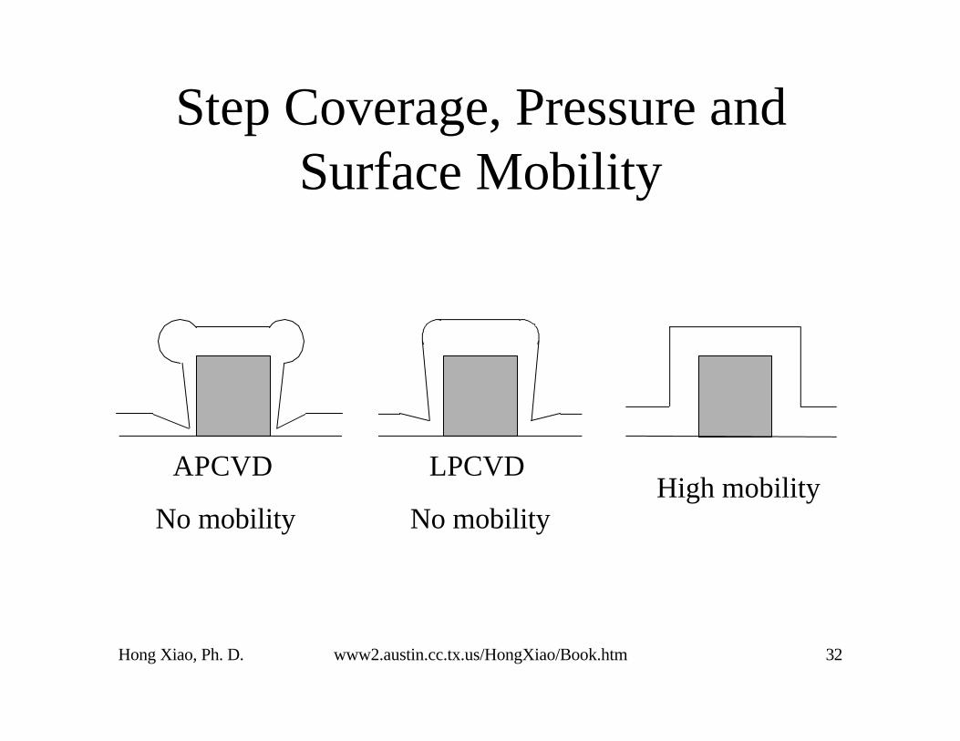
Step Coverage, Pressure andSurface Mobility
APCVD
No mobility
LPCVD
No mobilityHigh mobility

Hong Xiao, Ph. D. www2.austin.cc.tx.us/HongXiao/Book.htm 33
Silicon
PSG
Nitride
Largerarrivingangle
Smallerarrivingangle
Arriving Angles, Contact Holes

Hong Xiao, Ph. D. www2.austin.cc.tx.us/HongXiao/Book.htm 34
Gap Fill
• Fill a gap without voids
• Voids: cause defect and reliability problems
• Deposition/Etchback/Deposition– Silane and PE-TEOS film
• Conformal deposition– O3-TEOS and tungsten CVD
• High density plasma CVD

Hong Xiao, Ph. D. www2.austin.cc.tx.us/HongXiao/Book.htm 35
Gap Fill
• PMD: zero tolerance voids– Tungsten can be deposited into these voids
– Causing shorts
• IMD: voids below metal may tolerable– reducing κ– process gas could come out later and cause
reliability problem
Hong Xiao, Ph. D. www2.austin.cc.tx.us/HongXiao/Book.htm 36
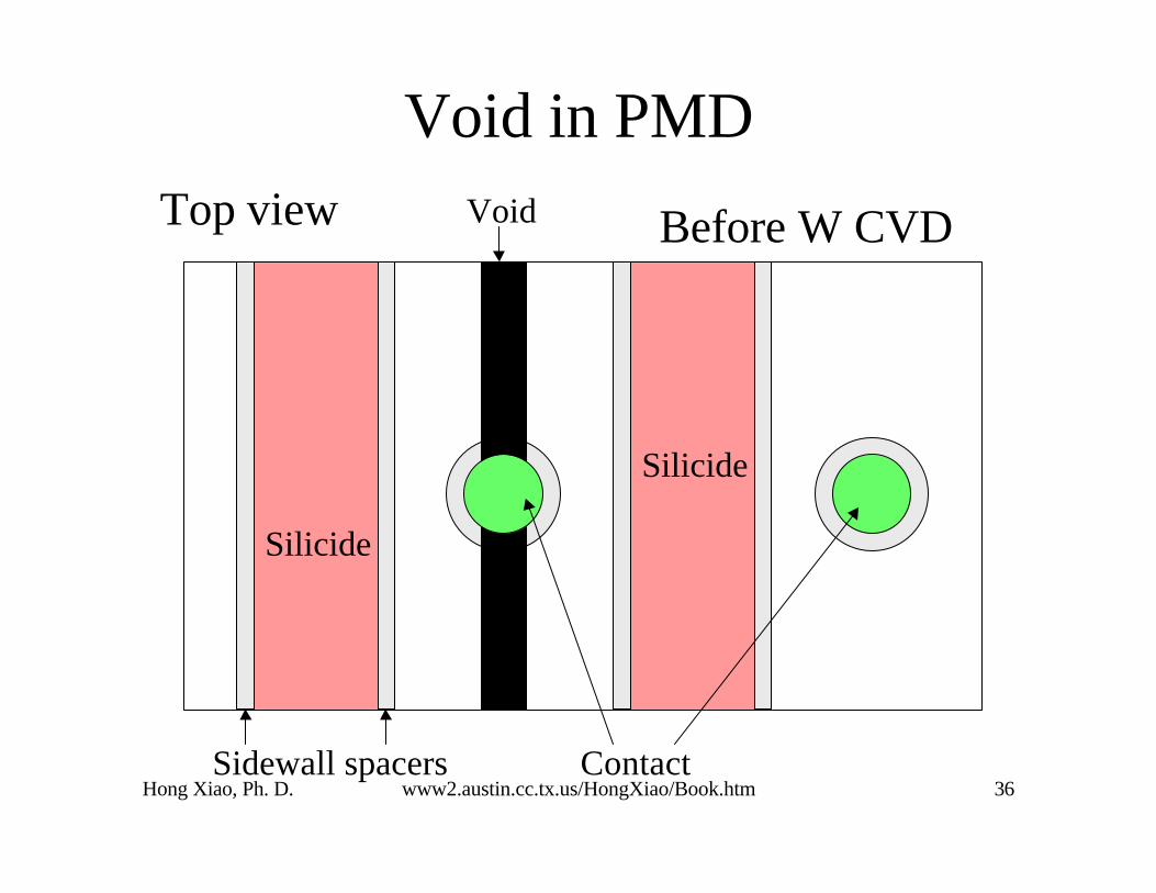
Void in PMD
Silicide
Void
Silicide
Top view Before W CVD
ContactSidewall spacers

Hong Xiao, Ph. D. www2.austin.cc.tx.us/HongXiao/Book.htm 37
Unwanted W Line Between Gates
Silicide
Tungsten
Silicide
Top view After W CVD
W plugSidewall spacers

Hong Xiao, Ph. D. www2.austin.cc.tx.us/HongXiao/Book.htm 38
Deposition/Etchback/Deposition
Al·Cu
Al·Cu
Al·Cu
USG
USG
USG
Dep.
Dep.
Etch

Hong Xiao, Ph. D. www2.austin.cc.tx.us/HongXiao/Book.htm 39
Conformal Deposition Gap Fill

Hong Xiao, Ph. D. www2.austin.cc.tx.us/HongXiao/Book.htm 40
Conformal Deposition Gap Fill

Hong Xiao, Ph. D. www2.austin.cc.tx.us/HongXiao/Book.htm 41
Conformal Deposition Gap Fill

Hong Xiao, Ph. D. www2.austin.cc.tx.us/HongXiao/Book.htm 42
Metal MetalMetal
Metal MetalMetal
Metal MetalMetal
HDP CVD Gap Fill

Hong Xiao, Ph. D. www2.austin.cc.tx.us/HongXiao/Book.htm 43
Surface Adsorption
• Determine precursors surface mobility
• Affect step coverage and gap fill
• Physical adsorption (physisorption)
• Chemical adsorption (chemisorption)

Hong Xiao, Ph. D. www2.austin.cc.tx.us/HongXiao/Book.htm 44
Chemisorption
• Actual chemical bonds between surface atomand the adsorbed precursor molecule
• Bonding energy usually exceeding 2 eV
• Low surface mobility
• Ion bombardment with10 to 20 eV energy inPECVD processes can cause some surfacemigration of chemisorbed precursors

Hong Xiao, Ph. D. www2.austin.cc.tx.us/HongXiao/Book.htm 45
Physisorption
• Weak bond between surface and precursor
• Bonding energy usually less than 0.5 eV– Hydrogen bonding
– Van der Waals forces
• Ion bombardment and thermal energy at 400 °Ccan cause migration of physisorbed precursors
• High surface mobility

Hong Xiao, Ph. D. www2.austin.cc.tx.us/HongXiao/Book.htm 46
Distancefrom surface
Bondingenergy
Substrate Surface
Chemisorbed precursor
Physisorbed precursor
Adsorptions

Hong Xiao, Ph. D. www2.austin.cc.tx.us/HongXiao/Book.htm 47
Dielectric CVD Precursors
• Silane (SiH4)
• TEOS (tetra-ethyl-oxy-silane, Si(OC2H5)4)

Hong Xiao, Ph. D. www2.austin.cc.tx.us/HongXiao/Book.htm 48
CVD Precursor: Silane
• Dielectric CVD– PECVD passivation dielectric depositions
– PMD barrier nitride layer
– Dielectric anti reflective coating (DARC)
– High density plasma CVD oxide processes
• LPCVD poly-Si and silicon nitride
• Metal CVD– W CVD process for nucleation step
– Silicon source for WSix deposition
Hong Xiao, Ph. D. www2.austin.cc.tx.us/HongXiao/Book.htm 49
Dielectric CVD Precursor: Silane
• Pyrophoric (ignite itself), explosive, and toxic
• Open silane line without thoroughly purgingcan cause fire or minor explosion and dust line

Hong Xiao, Ph. D. www2.austin.cc.tx.us/HongXiao/Book.htm 50
H
Si
H
H
H
Structure of Silane Molecule
Si
H
H
H H

Hong Xiao, Ph. D. www2.austin.cc.tx.us/HongXiao/Book.htm 51
CVD Precursor Adsorption: Silane
• Silane molecule is perfectly symmetrical
• Neither chemisorb nor physisorb
• Fragments of silane, SiH3, SiH2, or SiH, caneasily form chemical bonds with surface
• Low surface mobility, overhangs and poor stepcoverage

Hong Xiao, Ph. D. www2.austin.cc.tx.us/HongXiao/Book.htm 52
CVD Precursor Adsorption: TEOS
• TEOS (tetra-ethyl-oxy-silane, Si(OC2H5)4)
• Big organic molecule
• TEOS molecule is not perfectly symmetric
• Can form hydrogen bond and physisorb
• High surface mobility
• Good step coverage, conformality, and gap fill
• Widely used for oxide deposition

Hong Xiao, Ph. D. www2.austin.cc.tx.us/HongXiao/Book.htm 53
Si
H
H
H H
H
H H
H
C
C
O
O
H
H H
H
C
C
C C O C CO
HH HH
H HH H
TEOS Molecule

Hong Xiao, Ph. D. www2.austin.cc.tx.us/HongXiao/Book.htm 54
TEOS Applications
• STI, sidewall spacer, PMD, and IMD
• Most dielectric CVD processes are TEOSbased oxide processes

Hong Xiao, Ph. D. www2.austin.cc.tx.us/HongXiao/Book.htm 55
1
3
10
30
100
10 20 30 40 50 60 70 80 90 100 110
Vap
or P
ress
ure
(Tor
r)
Temperature (°C)
TEOS Vapor Pressure
1
3
10
30
100

Hong Xiao, Ph. D. www2.austin.cc.tx.us/HongXiao/Book.htm 56
TEOS Delivery
• A liquid at room temperature with boilingpoint at the sea level is 168 °C– As a reference, boiling point of water (H2O) at sea
level is 100 °C
• Need delivery system to send its vapor toprocess chamber
• Boiler, bubbler, and injection systems

Hong Xiao, Ph. D. www2.austin.cc.tx.us/HongXiao/Book.htm 57
MFC Processchamber Pump
TEOS
Thermostatic oven
Heated gas line Heated foreline
Boiler System

Hong Xiao, Ph. D. www2.austin.cc.tx.us/HongXiao/Book.htm 58
LiquidTEOS
Thermostaticoven
MFC MFM Processchamber
Pump
Carrier gas
Carrier gasbubbles
Heated gas line
Bubbler System

Hong Xiao, Ph. D. www2.austin.cc.tx.us/HongXiao/Book.htm 59
LFC Processchamber
Pump
MFCCarriergas
Injectionvalve
Liquid TEOS
Pressurizegas
Liquid TEOSflow Heated gas
line, TEOSvapor andcarrier gas
Injection System

Hong Xiao, Ph. D. www2.austin.cc.tx.us/HongXiao/Book.htm 60
Sticking Coefficient
• The probability that precursor atom formschemical bond with surface atom in onecollision
• Can be calculated by comparing the calculateddeposition rate with 100% sticking coefficientand the measured actual deposition rate

Hong Xiao, Ph. D. www2.austin.cc.tx.us/HongXiao/Book.htm 61
Sticking Coefficient
Precursors Sticking Coefficient
SiH4 3×10⁻⁴ to 3×10⁻⁵
SiH3 0.04 to 0.08
SiH2 0.15
SiH 0.94
TEOS 10-3
WF6 10-4

Hong Xiao, Ph. D. www2.austin.cc.tx.us/HongXiao/Book.htm 62
Step Coverage of TEOS and Silane Oxide
TEOS
Silane
Hong Xiao, Ph. D. www2.austin.cc.tx.us/HongXiao/Book.htm 63
Question
• Why don’t people apply TEOS as thesilicon source gas for the silicon nitridedeposition to get better step coverage for thenitride film

Hong Xiao, Ph. D. www2.austin.cc.tx.us/HongXiao/Book.htm 64
Answer
• In the TEOS molecule, the silicon atom isbonded with four oxygen atoms. It is almostimpossible to strip all oxygen atoms andhave silicon bonded only with nitrogen.Therefore, TEOS is mainly used for theoxide deposition and the nitride depositionnormally uses silane as the silicon sourcegas

Hong Xiao, Ph. D. www2.austin.cc.tx.us/HongXiao/Book.htm 65
Chemical Reaction Rate
∆Η
Ea
Precursor
Byproduct
C.R. = A exp (-Ea/kT)
Hong Xiao, Ph. D. www2.austin.cc.tx.us/HongXiao/Book.htm 66
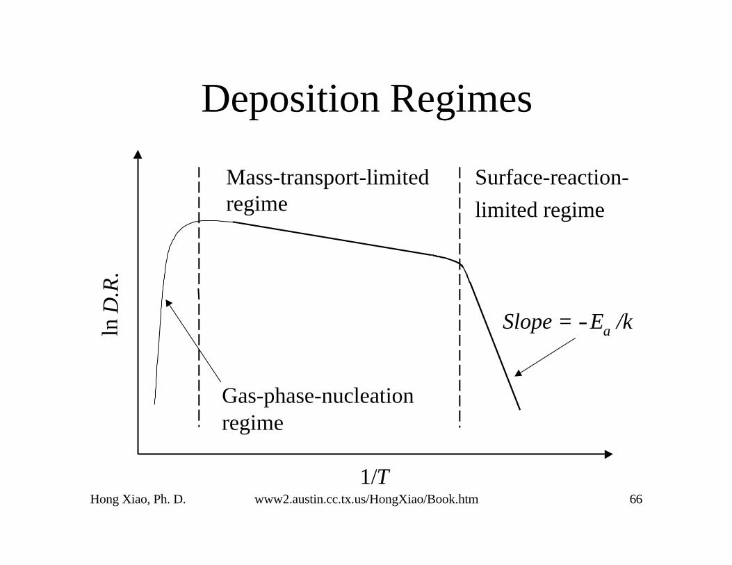
Deposition Regimes
1/T
ln D
.R.
Mass-transport-limitedregime
Surface-reaction-
limited regime
Slope = −Ea /k
Gas-phase-nucleationregime

Hong Xiao, Ph. D. www2.austin.cc.tx.us/HongXiao/Book.htm 67
Surface-Reaction-Limited Regime
• Chemical reaction rate can’t match precursordiffusion and adsorption rates; precursors pileup on the substrate surface and wait their turnto react.
D.R. = C.R. [B] [C] []…• Deposition rate is very sensitive to temperature

Hong Xiao, Ph. D. www2.austin.cc.tx.us/HongXiao/Book.htm 68
Mass-Transport-Limited Regime
• When the surface chemical reaction rate is highenough, the chemical precursors reactimmediately when they adsorb on the substratesurface.
• Deposition rate = D dn/dx [B] [C] []…• Deposition rate is insensitive to temperature
• Mainly controlled by gas flow rates

Hong Xiao, Ph. D. www2.austin.cc.tx.us/HongXiao/Book.htm 69
Temperature
Dep
osit
ion
rate Dep. rate
insensitive totemperature
Dep. ratesensitive totemperature
Deposition Rage Regimes

Hong Xiao, Ph. D. www2.austin.cc.tx.us/HongXiao/Book.htm 70
CVD Reactor Deposition Regime
• Most single wafer process reactors aredesigned in mass-transport-limited regime
• It is easier to control the gas flow rate
• Plasma or unstable chemicals such as ozoneare used to achieve mass-transport-limited-regime at relatively low temperature

Hong Xiao, Ph. D. www2.austin.cc.tx.us/HongXiao/Book.htm 71
Applications of Dielectric Thin film
• Shallow trench isolation (STI, USG)
• Sidewall Spacer (USG)
• Pre-metal dielectric (PMD, PSG or BPSG)
• Inter-metal dielectric (IMD, USG or FSG)
• Anti-reflection coating (ARC, SiON)
• Passivation dielectric (PD, Oxide/Nitride)

Hong Xiao, Ph. D. www2.austin.cc.tx.us/HongXiao/Book.htm 72
Dielectric CVD, Oxide and Nitride
Oxide (SiO2) Nitride (Si3N4)
Similar dielectric strength, > 1×10⁷
V/cmSimilar dielectric strength, > 1×10⁷ V/cm
Lower dielectric constant, κ = 3.9 Higher dielectric constant, κ = 7.0
Not a good barrier for moisture andmobile ion (Na+)
Good barrier for moisture and mobile ion(Na+)
Transparent to UV Conventional nitride opaque to UV
Can be doped with P and B

Hong Xiao, Ph. D. www2.austin.cc.tx.us/HongXiao/Book.htm 73
Shallow Trench Isolation (STI)
Grow pad oxideDeposition nitride
Etch nitride,oxide andsilicon
Grow barrieroxide
CVD USGtrench fill
CMP USGAnneal USG
Si Si Si Si Si
Strip nitrideand oxide
USG USG USG

Hong Xiao, Ph. D. www2.austin.cc.tx.us/HongXiao/Book.htm 74
Shallow Trench Isolation (STI)

Hong Xiao, Ph. D. www2.austin.cc.tx.us/HongXiao/Book.htm 75
Sidewall Spacer Formation
Substrate
Poly gate
Oxide
Substrate
Poly gate
Sidewall spacer
•Lightly doped drain (LDD)
•Self aligned silicide (Salicide)

Hong Xiao, Ph. D. www2.austin.cc.tx.us/HongXiao/Book.htm 76
PMD
• Doped oxide
• PSG or BPSG
• Phosphorus: gettering sodium and reduce flowtemperature.
• Boron: further reduces flow temperature withoutexcessive phosphorus

Hong Xiao, Ph. D. www2.austin.cc.tx.us/HongXiao/Book.htm 77
Sodium Ion Turn-on the MOSFET
Source Drainp-Si
n+ n+
“Metal” Gate
SiO2
Source Drainp-Si
VDVG = 0
Normal off
“Metal” Gate
Thin oxide
VD > 0VG = 0
+ + + + + + + +− − − − − − − −
Electron flow
Sodium ions
ElectronsTurn on by Na +
n+ n+

Hong Xiao, Ph. D. www2.austin.cc.tx.us/HongXiao/Book.htm 78
PMD
• More phosphorus, lower reflow temperature
• >7wt% phosphorus, hygroscope
P2O5 + 3H2O → 2H3PO4
• H3PO4 etches aluminum causes metal corrosion
• Too much boron will cause crystallization ofboric acid. H3BO3.
• Limit, P% + B% < 10%

Hong Xiao, Ph. D. www2.austin.cc.tx.us/HongXiao/Book.htm 79
Question
• Silicon nitride is a better sodium barrierlayer than silicon oxide. Why don’t peoplejust use nitride for PMD layer?

Hong Xiao, Ph. D. www2.austin.cc.tx.us/HongXiao/Book.htm 80
Answer
• Silicon nitride has higher dielectric constant
• Using nitride can cause longer RC timedelay and reduce circuit speed
• A thin layer of nitride (~ 200 Å) iscommonly used as a diffusion barrier layerin the PMD application
• Prevent diffusion of phosphorus and boronfrom BPSG diffusing into source/drain

Hong Xiao, Ph. D. www2.austin.cc.tx.us/HongXiao/Book.htm 81
PSG Reflow at 1100 °C, N2, 20 min.
0%
4.6%
2.2%
7.2%
Source: VLSI Technology, by S.M. Sze

Hong Xiao, Ph. D. www2.austin.cc.tx.us/HongXiao/Book.htm 82
Some Facts about SodiumName Sodium
Symbol NaAtomic number 11Atomic weight 22.989770
Discoverer Sir Humphrey DavyDiscovered at EnglandDiscovery date 1807Origin of name From the English word "soda" (the origin of the
symbol Na comes from the Latin word "natrium")Density of solid 0.968 g/cm3
Molar volume 23.78 cm3
Velocity of sound 3200 m/secElectrical resistivity 4.7 µΩ⋅cm
Reflectivity No dataMelting point 97.72 °CBoiling point 882.85 °C
Thermal conductivity 140 W m-1 K-1
Coefficient of linear thermalexpansion
71×10-6 K-1
Applications Major contaminant, needs to be strictly controlledMain removal agent HCl
Barrier materials used Silicon nitride and PSG

Hong Xiao, Ph. D. www2.austin.cc.tx.us/HongXiao/Book.htm 83
4×4 BPSG Reflow at 850 °C, 30Minutes in N2 Ambient

Hong Xiao, Ph. D. www2.austin.cc.tx.us/HongXiao/Book.htm 84
Development of PMD Processes
Dimension PMD Planarization Reflow temperature
> 2 µm PSG Reflow 1100°C
2 - 0.35 µm BPSG Reflow 850 - 900°C
0.25 µm BPSG Reflow + CMP 750°C
0.18 µm PSG CMP -

Hong Xiao, Ph. D. www2.austin.cc.tx.us/HongXiao/Book.htm 85
PMD Applications Roadmap
WaferSize (mm)
0.8 0.5
150
0.35 0.25 0.18
200 300
PE-TEOS BPSG
Thermal Flow or RTP/CMP
O3-TEOS PSG + PE-PSG
CMP
HDP PSG + PE-PSGCMP
LPCVD BPSG
O3-TEOS BPSG
FeatureSize (µm)
1995 199819921989 2000Year
Thermal Flow
APCVD Silane BPSG
Low-k DielectricCMP

Hong Xiao, Ph. D. www2.austin.cc.tx.us/HongXiao/Book.htm 86
IMD
• Inter-metal dielectric
• Undoped silicate glass (USG) or FSG
• SOG
• Gap fill and planarization
• Temperature limited by metal melting– Normally 400 °C
• PE-TEOS, O3-TEOS, and HDP

Hong Xiao, Ph. D. www2.austin.cc.tx.us/HongXiao/Book.htm 87
TEOS
• Tetraethyloxysilane,Si(OC2H5)4
• Liquid silicon source
• Commonly used forSiO2 deposition
• Good step coverageand gap fill
Si
H
H
H H
H
H H
H
C
C
O
O
H
H H
H
C
C
C C O C CO
HH HH
H HH H

Hong Xiao, Ph. D. www2.austin.cc.tx.us/HongXiao/Book.htm 88
PE-TEOS
• Plasma-enhanced TEOS CVD processes
• TEOS and O2
• Most commonly used dielectric CVD process
• Deposit USG at ~400 °C
• Mainly for IMD
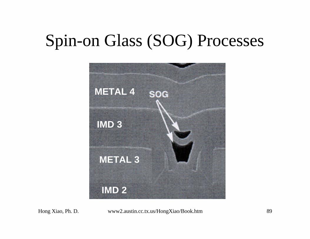
Hong Xiao, Ph. D. www2.austin.cc.tx.us/HongXiao/Book.htm 89
METAL 3
METAL 4
IMD 3
IMD 2
Spin-on Glass (SOG) Processes

Hong Xiao, Ph. D. www2.austin.cc.tx.us/HongXiao/Book.htm 90
PE-TEOS
• PE-TEOS
• Sputteringetchback
• PE-TEOS
Photo courtesy:Applied Materials

Hong Xiao, Ph. D. www2.austin.cc.tx.us/HongXiao/Book.htm 91
O3-TEOS
• TEOS and Ozone
• O3 → O2 + O (half-life time: 86 hours at 22 °C,< 1ms at 400 °C)
• O + TEOS → USG + other volatile byproducts
• Excellent step coverage and gap fill.
• Applied for IMD and PMD

Hong Xiao, Ph. D. www2.austin.cc.tx.us/HongXiao/Book.htm 92
O3-TEOS vs PE-TEOS
PE-TEOS Ozone-TEOS
Step coverage: 50% Step coverage: 90%Conformality: 87.5% Conformality: 100%

Hong Xiao, Ph. D. www2.austin.cc.tx.us/HongXiao/Book.htm 93
High Density Plasma CVD
• HDP-CVD: deposition and sputtering etch atthe same time.
• USG for STI application
• USG and FSG for IMD applications
• PMD for PMD application

Hong Xiao, Ph. D. www2.austin.cc.tx.us/HongXiao/Book.htm 94
Metal MetalMetal
HDP-CVD, IMD Application

Hong Xiao, Ph. D. www2.austin.cc.tx.us/HongXiao/Book.htm 95
Metal MetalMetal
Oxide CMP
Hong Xiao, Ph. D. www2.austin.cc.tx.us/HongXiao/Book.htm 96
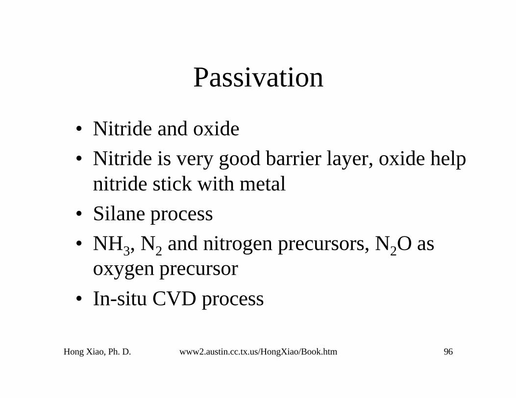
Passivation
• Nitride and oxide
• Nitride is very good barrier layer, oxide helpnitride stick with metal
• Silane process
• NH3, N2 and nitrogen precursors, N2O asoxygen precursor
• In-situ CVD process

Hong Xiao, Ph. D. www2.austin.cc.tx.us/HongXiao/Book.htm 97
Dielectric Thin FilmCharacteristics
• Refractive index
• Thickness
• Uniformity
• Stress
• Particles

Hong Xiao, Ph. D. www2.austin.cc.tx.us/HongXiao/Book.htm 98
Refractive Index
Speed of light in vacuumRefractive index, n =
Speed of light in the film

Hong Xiao, Ph. D. www2.austin.cc.tx.us/HongXiao/Book.htm 99
θ1
θ2Refractive light
Vacuumn1
Filmn2
Incident light
n1 sin θ1 = n2 sin θ2
Refractive Index

Hong Xiao, Ph. D. www2.austin.cc.tx.us/HongXiao/Book.htm 100
SiO2
Refractive index
Si3N4
Polysilicon
1.46
2.01
4.0
Oxygen rich
Oxygen richNitrogen rich
Oxygen richNitrogen rich
Nitrogen richSilicon rich
Silicon rich
Oxynitride
Film Information from R.I.

Hong Xiao, Ph. D. www2.austin.cc.tx.us/HongXiao/Book.htm 101
Linearly Polarized Incident Light
Elliptically PolarizedReflected Light
n1, k1, t1
n2, k2
sp
Ellipsometry R.I. Measurement

Hong Xiao, Ph. D. www2.austin.cc.tx.us/HongXiao/Book.htm 102
Laser light Photo detector
Substrate
Coupling head
Thin film θ
Illustration of Prism Coupler

Hong Xiao, Ph. D. www2.austin.cc.tx.us/HongXiao/Book.htm 103
θ
Refle
cted
Inten
sity
20° 10° 0° -10° -20°
Reflected Light Intensity vs.Incidence Angle
Modes

Hong Xiao, Ph. D. www2.austin.cc.tx.us/HongXiao/Book.htm 104
Metricon Model 2010 PrismCoupler

Hong Xiao, Ph. D. www2.austin.cc.tx.us/HongXiao/Book.htm 105
Comparison of the Two Methods
Ellipsometry
• Need know rough filmthickness before hand
• Can measure thicknessif R.I. is know
Prism coupler
• Need certain thicknessof the film, > 3000 Å
• Can measure thicknessif film thick enough tosupport enough modes

Hong Xiao, Ph. D. www2.austin.cc.tx.us/HongXiao/Book.htm 106
Thickness Measurement
• One of the most important measurementsfor dielectric thin film processes.
• Determines– Film deposition rate
– Wet etch rate
– Shrinkage

Hong Xiao, Ph. D. www2.austin.cc.tx.us/HongXiao/Book.htm 107
Dielectric Thin Film ThicknessMeasurement
t
21
Substrate
Dielectric film, n(λ)
Incident lightHuman eye orphotodetector

Hong Xiao, Ph. D. www2.austin.cc.tx.us/HongXiao/Book.htm 108
Dielectric Thin Film ThicknessMeasurement
• Different thickness has different color
• Tilting wafer also changes the color

Hong Xiao, Ph. D. www2.austin.cc.tx.us/HongXiao/Book.htm 109
Question
• If you see some beautiful color rings on a waferwith a CVD dielectric layer, what is yourconclusion?

Hong Xiao, Ph. D. www2.austin.cc.tx.us/HongXiao/Book.htm 110
Answer
• Color change indicates the dielectric thin filmthickness change, thus we know the film withthe color rings must have problem withthickness uniformity, which is most likelycaused by a non-uniform thin film depositionprocess.

Hong Xiao, Ph. D. www2.austin.cc.tx.us/HongXiao/Book.htm 111
Question
• Why does the thin film color change when onelook at the wafer from different angle?

Hong Xiao, Ph. D. www2.austin.cc.tx.us/HongXiao/Book.htm 112
Answer
• When one looking at wafer from a differentangle, phase shift will change, thus wavelengthfor constructive interference will change, whichcauses color change
• It is important to hold the wafer straight whenusing the color chart to measure film thickness
• Tilt wafer makes the film thickness thicker thanit actually is

Hong Xiao, Ph. D. www2.austin.cc.tx.us/HongXiao/Book.htm 113
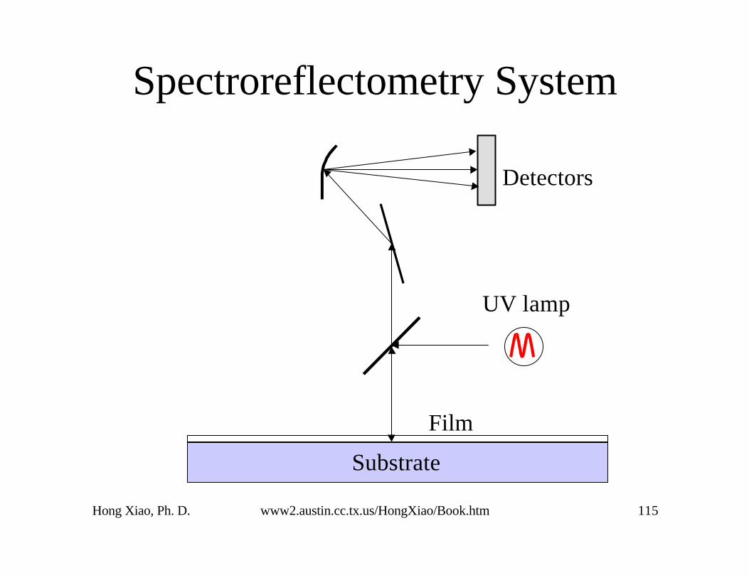
Spectroreflectometry
• Measure the reflected light intensity at differentwavelengths
• Calculate thin film thickness from therelationship between reflected light intensity andwavelength.
• Photodetector is more sensitive than human eyes
• Spectroreflectometry can obtain much higherresolution and accuracy for the film thickness

Hong Xiao, Ph. D. www2.austin.cc.tx.us/HongXiao/Book.htm 114
Relation of Reflectance and Wavelength
λ1 λ2 λ3
358 417 476 535 594 653 712 771
Ref
lect
ance
(%
)
05
101520253035404550
Wavelength (nm)
Constructive interferenceDestructive interference
ntmm 2
111
1
=−+λλ
Hong Xiao, Ph. D. www2.austin.cc.tx.us/HongXiao/Book.htm 115
Spectroreflectometry System
Substrate
UV lamp
Detectors
Film

Hong Xiao, Ph. D. www2.austin.cc.tx.us/HongXiao/Book.htm 116
Question
• Many advance thin film thicknessmeasurement tools allows user to choosethe refractive index of the film. If someonemistakenly chooses the PE-TEOS USG filmrefractive index to measure O3-TEOS USGfilms thickness, what will be the effect onthe measurement result?

Hong Xiao, Ph. D. www2.austin.cc.tx.us/HongXiao/Book.htm 117
Answer
• Since the nt always coupled together
• A wrong n will cause wrong t measurement
• O3-TEOS USG is a porous film and has aR.I., about 1.44
• Slightly lower than 1.46 of PE-TEOS USG
• Measured O3-TEOS film thickness will beslightly thinner than its actual value

Hong Xiao, Ph. D. www2.austin.cc.tx.us/HongXiao/Book.htm 118
Deposition Rate
Thickness of deposited film
Deposition timeDeposition Rate =

Hong Xiao, Ph. D. www2.austin.cc.tx.us/HongXiao/Book.htm 119
Wet Etch Rate
Thickness change of the CVD film Wet etch rate ratio =
Thickness change of the thermal oxide film
Thickness change after etchWet Etch Rate =
Etch time

Hong Xiao, Ph. D. www2.austin.cc.tx.us/HongXiao/Book.htm 120
Uniformity
• Multi-point measurement• Definition
• Average:
• Standard deviation:
• Standard deviation non-uniformity: σ/x
Nxxxx
x N+⋅⋅⋅+++= 321
1
)()()()( 223
22
21
−−+⋅⋅⋅+−+−+−
=N
xxxxxxxx Nσ

Hong Xiao, Ph. D. www2.austin.cc.tx.us/HongXiao/Book.htm 121
Stress
• Mismatch between different materials
• Two kinds of stresses, intrinsic and extrinsic
• Intrinsic stress develops during the filmnucleation and growth process.
• The extrinsic stress results from differencesin the coefficients of thermal expansion
• Tensile stress: cracking film if too high
• Compressive stress: hillock if too strong

Hong Xiao, Ph. D. www2.austin.cc.tx.us/HongXiao/Book.htm 122
Bare Wafer After Thin Film Deposition
Compressive StressNegative curvature
Tensile StressPositive curvature
Substrate SubstrateSubstrate
Film Stress

Hong Xiao, Ph. D. www2.austin.cc.tx.us/HongXiao/Book.htm 123
Illustration of Thermal Stress
SiO2
Si
∆L
SiO2
Si
At 400 °C
At Room Temperature
L
∆L = α ∆T L

Hong Xiao, Ph. D. www2.austin.cc.tx.us/HongXiao/Book.htm 124
Coefficients of Thermal Expansion
α(SiO2) = 0.5×10⁻⁶ °C−1
α(Si) = 2.5×10⁻⁶ °C−1
α(Si3N4) = 2.8×10⁻⁶ °C−1
α(W) = 4.5×10⁻⁶ °C−1
α(Al) = 23.2×10⁻⁶ °C−1

Hong Xiao, Ph. D. www2.austin.cc.tx.us/HongXiao/Book.htm 125
Stress Measurement
)11
(61 12
2
RRthE
−−
=ν
σ
Wafer curvature change before and after thinfilm deposition
Laser beam scans wafer surface, reflectionlight indicates the wafer curvature
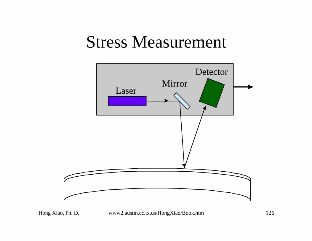
Hong Xiao, Ph. D. www2.austin.cc.tx.us/HongXiao/Book.htm 126
LaserMirror
Detector
Stress Measurement

Hong Xiao, Ph. D. www2.austin.cc.tx.us/HongXiao/Book.htm 127
Dielectric CVD Processes
• Thermal Silane CVD Process
• Thermal TEOS CVD Process
• PECVD Silane Processes
• PECVD TEOS Processes
• Dielectric Etchback Processes
• O3-TEOS Processes
• Spin-on Glass
• High Density Plasma CVD

Hong Xiao, Ph. D. www2.austin.cc.tx.us/HongXiao/Book.htm 128
Thermal Silane CVD Process
• Silane has been commonly used for silicondioxide deposition with both APCVD andLPCVD process
heat
SiH4 + 2 O2 → SiO2 + 2 H2O
• APCVD normally uses diluted silane (3% innitrogen) and LPCVD uses pure silane
• Not commonly used in the advanced fab

Hong Xiao, Ph. D. www2.austin.cc.tx.us/HongXiao/Book.htm 129
Thermal TEOS CVD Process
• TEOS: physisorption, high surface mobility
• TEOS film has better step coverage
• LPCVD TEOS dissociates at high temp: 700 °C
Si(OC2H5)4 → SiO2 + volatile organics
• BPSG with TMB and TMP for PMD
• Temperature is too high for IMD

Hong Xiao, Ph. D. www2.austin.cc.tx.us/HongXiao/Book.htm 130
PECVD Silane Processes
• Silane and N2O (laughing gas)• Dissociation in plasma form SiH2 and O• Radicals react rapidly to form silicon oxide
plasma
SiH4 + N2O → SiOxHy + H2O + N2 + NH3 + … heat
• Overflow N2O, using SiH4 flow to controldeposition rate

Hong Xiao, Ph. D. www2.austin.cc.tx.us/HongXiao/Book.htm 131
Question
• Can we overflow silane and use nitrousoxide flow rate to controlled depositionrate?

Hong Xiao, Ph. D. www2.austin.cc.tx.us/HongXiao/Book.htm 132
Answer
• Theoretically we can, but practically no oneshould even try this
• It is very dangerous and not cost effective
• Overflowing silane will create a big safetyhazard: fire and explosion
• Silane is more expensive than nitrous oxide
Hong Xiao, Ph. D. www2.austin.cc.tx.us/HongXiao/Book.htm 133
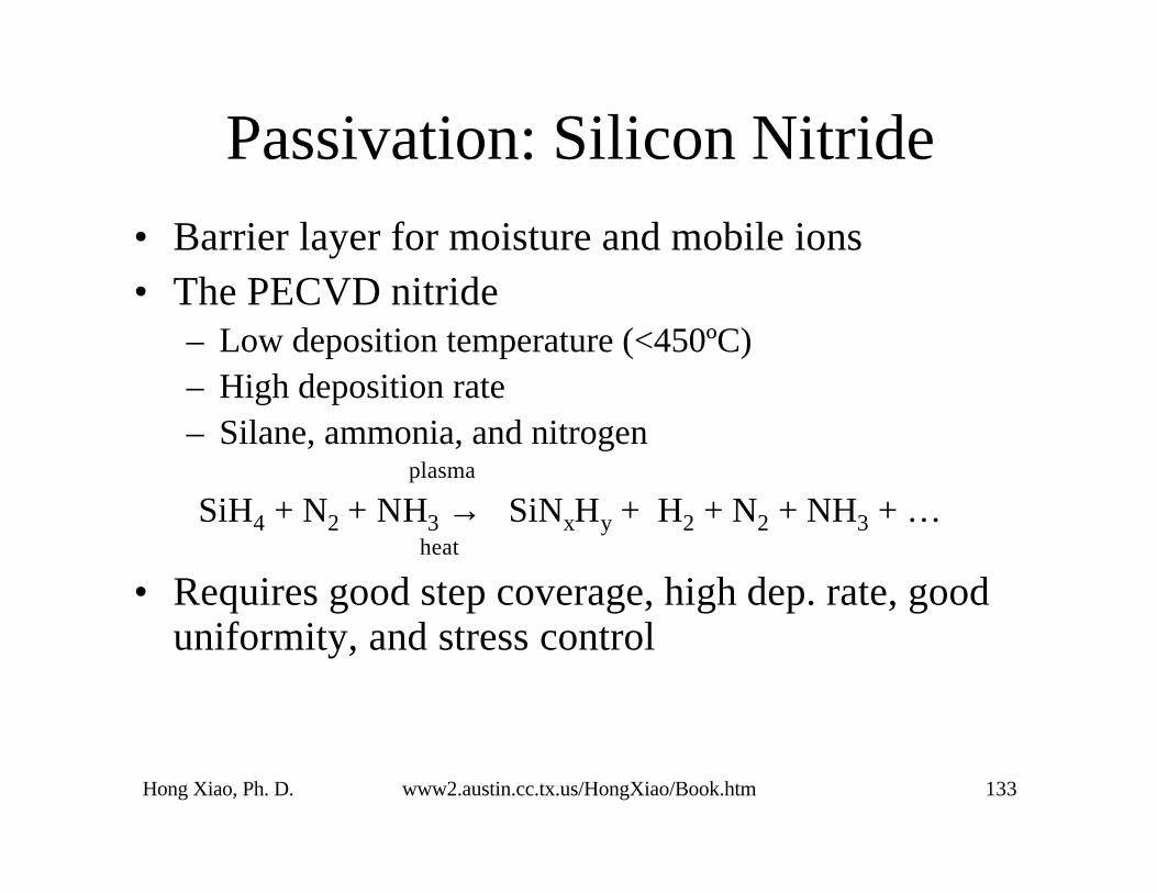
Passivation: Silicon Nitride
• Barrier layer for moisture and mobile ions• The PECVD nitride
– Low deposition temperature (<450ºC)– High deposition rate– Silane, ammonia, and nitrogen
plasma
SiH4 + N2 + NH3 → SiNxHy + H2 + N2 + NH3 + … heat
• Requires good step coverage, high dep. rate, gooduniformity, and stress control

Hong Xiao, Ph. D. www2.austin.cc.tx.us/HongXiao/Book.htm 134
Passivation Dielectric Deposition
• Stabilization 1 (stabilize pressure)
• Oxide deposition (stress buffer for nitride)
• Pump
• Stabilization 2 (stabilize pressure)
• Nitride deposition (passivation layer)
• Plasma purging (eliminate SiH4)
• Pump

Hong Xiao, Ph. D. www2.austin.cc.tx.us/HongXiao/Book.htm 135
EPROM Passivation Dielectric
• Need UV transparent passivation layer
• UV light can erase EPROM memory
• Oxynitride (SiOxNy) is commonly used
• Source gases: SiH4, N2, NH3, and N2Oplasma
SiH4 + N2 + NH3 + N2O → SiOxNy + H2O + N2 + … heat
• Properties in between oxide and nitride– UV transparent, and a fairly good barrier layer

Hong Xiao, Ph. D. www2.austin.cc.tx.us/HongXiao/Book.htm 136
PMD Barrier Layer
• PSG or BPSG need a diffusion barrier layer– USG (need 1000 Å)
– LPCVD nitride at ~700 ºC (~ 300 Å)
– PECVD nitride at <550 ºC (< 200 Å)
• At higher temperature, PECVD nitride film hashigher deposition rate, lower hydrogenconcentration, and better film quality
• Possible in future: remote plasma CVD
Hong Xiao, Ph. D. www2.austin.cc.tx.us/HongXiao/Book.htm 137
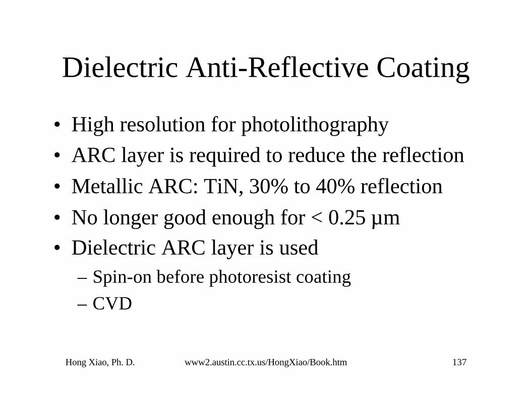
Dielectric Anti-Reflective Coating
• High resolution for photolithography
• ARC layer is required to reduce the reflection
• Metallic ARC: TiN, 30% to 40% reflection
• No longer good enough for < 0.25 µm
• Dielectric ARC layer is used– Spin-on before photoresist coating
– CVD

Hong Xiao, Ph. D. www2.austin.cc.tx.us/HongXiao/Book.htm 138
Dielectric Anti-Reflective Coating
t
21
Aluminum alloy
Dielectric ARC, n, k
UV light (λ)
Photoresist
∆φ = 2nt = λ/2

Hong Xiao, Ph. D. www2.austin.cc.tx.us/HongXiao/Book.htm 139
Dielectric ARC
• PECVD silane process
• N2O as oxygen and nitrogen source plasma
SiH4 + N2O + He → SiOxNy + H2O + N2 + NH3 +He + · · ·
heat

Hong Xiao, Ph. D. www2.austin.cc.tx.us/HongXiao/Book.htm 140
PE-TEOS
• Most widely used dielectric CVD process
• Fast
• Good uniformity
• Good step coverage
• Mainly used for IMD

Hong Xiao, Ph. D. www2.austin.cc.tx.us/HongXiao/Book.htm 141
PE-TEOS
• USG processPlasma
Si(OC2H5)4 + O2 → SiO2 + other volatiles400 ºC
• FGS process plasma
FSi(OC2H5)3 + Si(OC2H5)4 + O2 → SiOxFy + other volatile(FTES) (TEOS) heat (FSG)
Hong Xiao, Ph. D. www2.austin.cc.tx.us/HongXiao/Book.htm 142
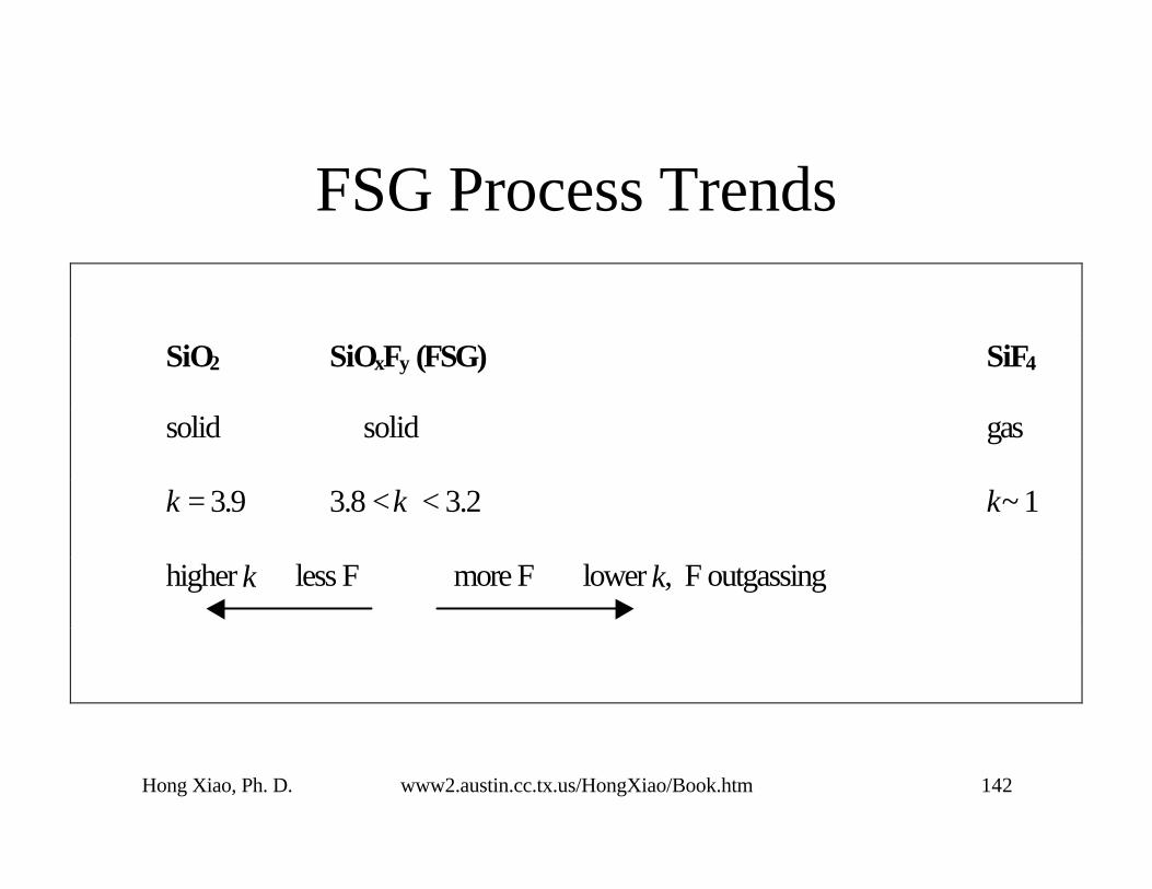
SiO2 SiOxFy (FSG) SiF4
solid solid gas
κ = 3.9 3.8 < κ < 3.2 κ~ 1
higher k less F more F lower k, F outgassing
FSG Process Trends

Hong Xiao, Ph. D. www2.austin.cc.tx.us/HongXiao/Book.htm 143
Dielectric Etchback Processes
• Gap fill and planarization
• Performed in thin film bay with DCVD
• Cluster tool
• In-situ dep/etch/dep process

Hong Xiao, Ph. D. www2.austin.cc.tx.us/HongXiao/Book.htm 144
C D
BAR
ob
ot
Cassette handler
Transfer chamber
CVD chambers
Sputter etch chamber
Sputter etch chamber
Dep.
Dep.
Etch
Metal
In-situ Dep/Etch/Dep Process

Hong Xiao, Ph. D. www2.austin.cc.tx.us/HongXiao/Book.htm 145
Sputtering Corner ChoppingAr+ Ar+

Hong Xiao, Ph. D. www2.austin.cc.tx.us/HongXiao/Book.htm 146
Question
• Why does sputtering etch process usuallyuse argon as the process gas?

Hong Xiao, Ph. D. www2.austin.cc.tx.us/HongXiao/Book.htm 147
Answer
• It is inert, heavy, and relative inexpensive
• The atomic weight of argon is 40, comparedwith silicon’s 28 and helium’s 4
• Argon is the third most abundant element inearth atmosphere (~ 1%) only after nitrogen(78%) and oxygen (20%)
• Can be purified directly from condensed air

Hong Xiao, Ph. D. www2.austin.cc.tx.us/HongXiao/Book.htm 148
Schematic of Sputtering EtchChamber
Process gases
PlasmaProcesschamber
By-products tothe pump
Chuck
RF power
Magnet coils

Hong Xiao, Ph. D. www2.austin.cc.tx.us/HongXiao/Book.htm 149
Reactive Etch Back
• CF4 and O2
• Heavy bombardment with chemical reaction
• Applications– Planarize dielectric surface
– SOG etch back

Hong Xiao, Ph. D. www2.austin.cc.tx.us/HongXiao/Book.htm 150
2 µm PE-TEOS oxide deposition
1 µm planarization etchback
Reactive Etch Back Planarization

Hong Xiao, Ph. D. www2.austin.cc.tx.us/HongXiao/Book.htm 151
O3-TEOS Processes
• Ozone is a very unstable molecule,
O3 → O2 + O
• At 400 °C, half-lifetime of O3: < 1ms
• Used as carrier of free oxygen radicals
• Ozone reacts with TEOS form silicon oxide
• Excellent conformality and gap fill capability
• Sub-micron IC chip applications
• APCVD and SA-CVD

Hong Xiao, Ph. D. www2.austin.cc.tx.us/HongXiao/Book.htm 152
Ozone Generation
plasma
O2 → O + O
O + O2 + M → O3 + M (M = O2, N2, Ar, He, etc.)
Lighting, corona discharge

Hong Xiao, Ph. D. www2.austin.cc.tx.us/HongXiao/Book.htm 153
O2 + N2 O2 + O3 + N2+ N2O + …
RF
Illustration of Ozonator

Hong Xiao, Ph. D. www2.austin.cc.tx.us/HongXiao/Book.htm 154
Monitored by UV absorption (Beer-Lambert law):
I = I0 exp(-XCL)
Ozone cell
L
O3/O2 O3/O2
Mechanical chopper UV sensor
Analyzer UV Lamp
Ozone Concentration Monitoring

Hong Xiao, Ph. D. www2.austin.cc.tx.us/HongXiao/Book.htm 155
O3-TEOS USG Process
• TEOS + O3 → SiO2 + volatile organics heat
• Main applications– STI (higher temperature, ~ 550 °C)
– IMD (~ 400 °C)

Hong Xiao, Ph. D. www2.austin.cc.tx.us/HongXiao/Book.htm 156
O3-TEOS USG
Step coverage Gap fill

Hong Xiao, Ph. D. www2.austin.cc.tx.us/HongXiao/Book.htm 157
O3-TEOS BPSG and PSG Process
O3 → O2 + O
O + TEB + TEPO + TEOS → BPSG + volatile organicsheat
O + TEPO + TEOS → PSG + volatile organicsheat
• Main application– PMD

Hong Xiao, Ph. D. www2.austin.cc.tx.us/HongXiao/Book.htm 158
O3-TEOS BPSG
SACVD BPSG for 0.25 µm gap and 4:1 A/R.
Silicide
Poly Si
BarrierNitride
O 3 -TEOSBPSG

Hong Xiao, Ph. D. www2.austin.cc.tx.us/HongXiao/Book.htm 159
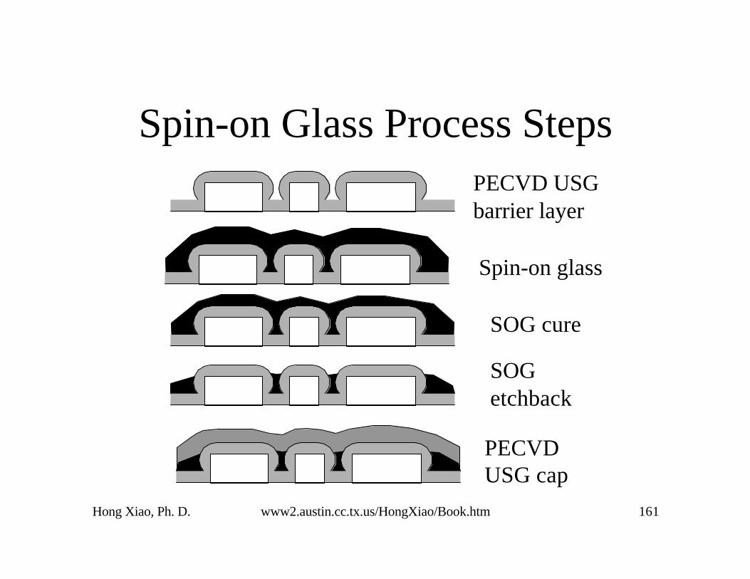
Spin-on Glass (SOG)
• Similar to PR coating and baking process
• People in fab like familiar technologies
• IMD gap fill and planarization
• Two kinds of spin-on glass:– Silicate
– Siloxane

Hong Xiao, Ph. D. www2.austin.cc.tx.us/HongXiao/Book.htm 160
Spin-on Glass: Silicate and Siloxane
Si
H
H
H H
O
O
O OSi
R’
R
H HO O
R = CH3, R’ = R or OH
Si(OH)4
Silicate
RnSi(OH)4-n, n = 1, 2
Siloxane
Hong Xiao, Ph. D. www2.austin.cc.tx.us/HongXiao/Book.htm 161
Spin-on Glass Process StepsPECVD USGbarrier layer
Spin-on glass
SOG cure
SOGetchback
PECVDUSG cap

Hong Xiao, Ph. D. www2.austin.cc.tx.us/HongXiao/Book.htm 162
High-Density Plasma CVD
• Dep/etch/dep gap fill needs two chambers
• Narrower gaps may need more dep/etchcycles to fill
• A tool can deposit and sputtering etchsimultaneously would be greatly helpful
• The solution: HDP-CVD

Hong Xiao, Ph. D. www2.austin.cc.tx.us/HongXiao/Book.htm 163
Question
• With the feature size shrinking, metal linewidth and gap between metal lines becomessmaller. However the metal line heightdoesn't shrink accordingly, which causeslarger gap aspect ratio.
• Why doesn’t shrink metal line heightaccordingly to keep the same aspect ratioand easier for dielectric gap fill?

Hong Xiao, Ph. D. www2.austin.cc.tx.us/HongXiao/Book.htm 164
Answer
• Metal line resistance R = ρ l/wh.
• If h also reduces accordingly to l and w,resistance will increase accordingly
• Therefore, line has to keep the same height

Hong Xiao, Ph. D. www2.austin.cc.tx.us/HongXiao/Book.htm 165
Inductively Coupled Plasma Chamber
Helium
Bias RF
Wafer
E-chuck
Plasma
Inductive coilsSource RF
Chamber body
Ceramic cover

Hong Xiao, Ph. D. www2.austin.cc.tx.us/HongXiao/Book.htm 166
ECR Chamber
Helium
Bias RF
Magneticfield line
Microwave
Magnetcoils Plasma
Wafer
E-chuck

Hong Xiao, Ph. D. www2.austin.cc.tx.us/HongXiao/Book.htm 167
Metal MetalMetal
HDP-CVD, IMD Application

Hong Xiao, Ph. D. www2.austin.cc.tx.us/HongXiao/Book.htm 168
Metal MetalMetal
HDP-CVD, Deposition

Hong Xiao, Ph. D. www2.austin.cc.tx.us/HongXiao/Book.htm 169
Metal MetalMetal
HDP-CVD, Deposition

Hong Xiao, Ph. D. www2.austin.cc.tx.us/HongXiao/Book.htm 170
Metal MetalMetal
HDP-CVD, Deposition

Hong Xiao, Ph. D. www2.austin.cc.tx.us/HongXiao/Book.htm 171
Metal MetalMetal
PE-TEOS Deposition

Hong Xiao, Ph. D. www2.austin.cc.tx.us/HongXiao/Book.htm 172
Metal MetalMetal
Oxide CMP

Hong Xiao, Ph. D. www2.austin.cc.tx.us/HongXiao/Book.htm 173
HDP-CVD Processes
• For IMD Applications
• USG SiH4 + O2 + Ar → USG + H2O + Ar +…
• FSG SiH4 + SiF4 + O2 + Ar → FSG + volatiles
• For PMD Applications
• PSG SiH4 + PH3 + O2 + Ar → PSG + volatiles

Hong Xiao, Ph. D. www2.austin.cc.tx.us/HongXiao/Book.htm 174
Question
• Why is silane instead of TEOS used as thesilicon source gas for the HDP CVD oxideprocess?

Hong Xiao, Ph. D. www2.austin.cc.tx.us/HongXiao/Book.htm 175
Answer
• For HDP CVD processes, step coverage isno longer an important factor for the gap fill
• Heavy ion bombardment always keeps gaptapered and deposition is bottom up.
• Using silane can save the costs and hasslesrelated with vapor delivery system of theliquid TEOS source.

Hong Xiao, Ph. D. www2.austin.cc.tx.us/HongXiao/Book.htm 176
Dielectric CVD Chamber Clean
• During dielectric CVD process, dielectricthin film will be deposited on everythinginside chamber
• Need to routinely clean the chamber toprevent particulate contamination problems.
• For DCVD, more time for clean than dep.
• RF plasma clean and remote plasma clean

Hong Xiao, Ph. D. www2.austin.cc.tx.us/HongXiao/Book.htm 177
RF Plasma Clean
• Plasma clean process remove dielectric filmon the process kits and chamber wall
• Fluorocarbon such as CF4, C2F6 and C3F8
• In some case NF3 is also used
• In plasma, fluorocarbon will be dissociated
• Free fluorine, F, will be generated
• F removes silicon oxide and silicon nitride

Hong Xiao, Ph. D. www2.austin.cc.tx.us/HongXiao/Book.htm 178
RF Clean Chemistry
plasma
CF4 → CF3 + F
plasma
F + SiO2 → SiF4 + Oheat
plasma
F + Si3N4 → SiF4 + Nheat

Hong Xiao, Ph. D. www2.austin.cc.tx.us/HongXiao/Book.htm 179
RF Clean Chemistry
• In plasma clean processes, oxygen sourcegases such as N2O and O2 are used withfluorocarbon to react with carbon and freemore fluorine radicals
• Increase F/C ratio, keep it > 2
• Prevent carbon fluoride polymerization, andincreases the clean efficiency

Hong Xiao, Ph. D. www2.austin.cc.tx.us/HongXiao/Book.htm 180
C
F
F C C
FF
F F
C C
FF
F F
C
F
F
F
F F
F
C
C
F FC F FC
CF2 and Reconnection

Hong Xiao, Ph. D. www2.austin.cc.tx.us/HongXiao/Book.htm 181
C
F
F
C
F
F
C C C C
FF FF
F FF F
C
F
F
C C
FF
F F
Polymerization, Teflon Deposition

Hong Xiao, Ph. D. www2.austin.cc.tx.us/HongXiao/Book.htm 182
RF Clean Endpoint
• Excitation-relaxation cause glow
• Different gases have different colors of light
• Information of chemical components in plasma
• Monitor line emission to control clean process

Hong Xiao, Ph. D. www2.austin.cc.tx.us/HongXiao/Book.htm 183
Endpoint Signal
0123456789
0 20 40 60 80 90 110Clean Time (sec)
Flu
orin
e P
eak
(407
nm
) In
tens
ity
Endpoint
Hong Xiao, Ph. D. www2.austin.cc.tx.us/HongXiao/Book.htm 184
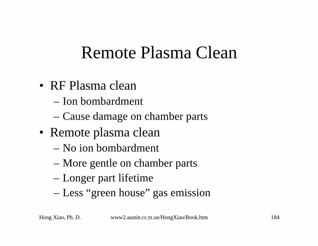
Remote Plasma Clean
• RF Plasma clean– Ion bombardment– Cause damage on chamber parts
• Remote plasma clean– No ion bombardment– More gentle on chamber parts– Longer part lifetime– Less “green house” gas emission

Hong Xiao, Ph. D. www2.austin.cc.tx.us/HongXiao/Book.htm 185
NF3 Plasma
F FF
F N2N2
F
Microwave
Processchamber
N2, SiF4,O2… To pump
Remote plasmachamber
Heated plate
Illustration of Remote Plasma Clean

Hong Xiao, Ph. D. www2.austin.cc.tx.us/HongXiao/Book.htm 186
Remote Plasma Clean
• Microwave (MW) power, NF3 as fluorine source• 99% of NF3 dissociated in MW plasma• Free fluorine reacts with the film in chamber
– No plasma inside process chamber– No ion bombardment– Prolongs their lifetime
• Disadvantages:– Less maturity, higher cost, and using NF3
– Can not use optical endpoint system, may need FTIRsystem to achieve the automatic process endpoint.

Hong Xiao, Ph. D. www2.austin.cc.tx.us/HongXiao/Book.htm 187
Process Trends and Troubleshooting
• Process response to input parameterschange
• Help to determine the root cause if somewrong

Hong Xiao, Ph. D. www2.austin.cc.tx.us/HongXiao/Book.htm 188
Silane PECVD Process Trends
• Increasing temperature increases depositionrate– Higher diffusion rate of precursors in boundary
layer
• Increasing temperature improves depositedstep coverage and film quality
• PMD uses a higher temperature• IMD and PD, normally not exceed 400 ºC

Hong Xiao, Ph. D. www2.austin.cc.tx.us/HongXiao/Book.htm 189
Deposition Rate and Temperature
Temperature
De
po
si
ti
on
Ra
te
Processwindow

Hong Xiao, Ph. D. www2.austin.cc.tx.us/HongXiao/Book.htm 190
Stress and RF Power
RF Power
Comp
ressive
Stress
Processwindow

Hong Xiao, Ph. D. www2.austin.cc.tx.us/HongXiao/Book.htm 191
Silane flow
Depos
it
ion
ra
te
Processwindow R
ef
ra
ct
iv
e
In
de
x
Silane PECVD Process Trends

Hong Xiao, Ph. D. www2.austin.cc.tx.us/HongXiao/Book.htm 192
Silane flow
St
re
ss
Processwindow
WERR
Silane PECVD Process Trends

Hong Xiao, Ph. D. www2.austin.cc.tx.us/HongXiao/Book.htm 193
RF power
Depos
ition rate
Free radicalsenhance reaction
Ion bombardmentreduce adsorption
Relationship of Deposition Rateand RF Power

Hong Xiao, Ph. D. www2.austin.cc.tx.us/HongXiao/Book.htm 194
Temperature
Dep
ositi
on
Rat
e
Dep. Rateinsensitive totemperature
Dep. Ratesensitive totemperature
Relationship of Deposition Rateand Temperature

Hong Xiao, Ph. D. www2.austin.cc.tx.us/HongXiao/Book.htm 195
PE-TEOS Trends
• RF power↑: dep rate↑↓, compressive stress↑– In process window, dep rate go down
• Temperature↑: dep rate↑↓– In process window, dep rare go down
• TEOS flow↑: dep rate↑, compressive stress↓

Hong Xiao, Ph. D. www2.austin.cc.tx.us/HongXiao/Book.htm 196
TEOS Flow
De
po
si
ti
on
Ra
te
Processwindow R
ef
ra
ct
iv
e
In
de
x
PE-TEOS Trends: TEOS Flow Rate

Hong Xiao, Ph. D. www2.austin.cc.tx.us/HongXiao/Book.htm 197
TEOS Flow
Compressi
ve St
ress
Processwindow
WERR
PE-TEOS Trends: TEOS Flow Rate

Hong Xiao, Ph. D. www2.austin.cc.tx.us/HongXiao/Book.htm 198
Temperature
Dep
ositi
on
Rat
e
400 to 550 °C
Increasingchemicalreactionrate
Reducingadsorption rate
PE-TEOS Trends: Temperature

Hong Xiao, Ph. D. www2.austin.cc.tx.us/HongXiao/Book.htm 199
O3-TEOS Trends
• Temperature↑: dep rate↑↓– In process window, dep rare go down
• TEOS flow↑: dep rate↑

Hong Xiao, Ph. D. www2.austin.cc.tx.us/HongXiao/Book.htm 200
Question
• For both PE- and O3- TEOS processes, themaximum deposition rate can be achieved atabout 250 ºC. Why do the IMD TEOSprocesses normally operate about 400 ºC andPMD and STI processes deposited evenhigher temperature (~ 550 ºC)?

Hong Xiao, Ph. D. www2.austin.cc.tx.us/HongXiao/Book.htm 201
Answer
• At higher deposition temperature, film qualityis higher and step coverage is better

Hong Xiao, Ph. D. www2.austin.cc.tx.us/HongXiao/Book.htm 202
Troubleshooting
• Learned from hand-on experience
• Sudden process change, either suddenly goeswrong, or gradually goes wrong and suddenlycomes back,
• Someone should check what has changedbetween good process and the bad process, orvice versa.

Hong Xiao, Ph. D. www2.austin.cc.tx.us/HongXiao/Book.htm 203
Troubleshooting
• Check metrology tool first and make sure theright recipe is used.
• If one measure PE-TEOS film with nitriderecipe, measured thickness would besignificantly thinner
• If nothing is wrong with metrology tool, thencheck whether the process recipe has beenchanged.

Hong Xiao, Ph. D. www2.austin.cc.tx.us/HongXiao/Book.htm 204
Troubleshooting
• Process always has problems at end of shift
• Someone should work cross shifts to find outwhat had been changed during shift change
• Something must be changed that put the processback to normal at the beginning of the next shift
• It most likely is the source of problems as theprocess gradually goes wrong at end of the shift

Hong Xiao, Ph. D. www2.austin.cc.tx.us/HongXiao/Book.htm 205
Troubleshooting
• Most dielectric CVD processes operate inmass-transport-limited regime
• Deposition rate is mainly determined by gasflow rate, usually silane and TEOS flow rate
• Very likely that deposition rate problems arerelated with silane or TEOS flow rate
• Mass flow controller and liquid flowcontroller

Hong Xiao, Ph. D. www2.austin.cc.tx.us/HongXiao/Book.htm 206
Troubleshooting: Non-uniformity
• Uniformity is determined by flow pattern
• If non-uniformity pattern is center symmetric– Adjusted spacing of the wafer and showerhead
– Or changing the carrier gas flow rate• Helium flow for TEOS processes
• Nitrogen flow for nitride process

Hong Xiao, Ph. D. www2.austin.cc.tx.us/HongXiao/Book.htm 207
Spacing and Film Profile
Showerhead
Wafer
Smaller spacing
Center thin profile
Larger spacing
Center thick profile
Normal spacing
Normal profile
Higher dep. rate
Normal dep. rate
Lower dep. rate

Hong Xiao, Ph. D. www2.austin.cc.tx.us/HongXiao/Book.htm 208
Troubleshooting: Non-uniformity
• If the non-uniformity is side-to-side
• Check wafer leveling or centering
• Leak check of slip valve of the chamber

Hong Xiao, Ph. D. www2.austin.cc.tx.us/HongXiao/Book.htm 209
Leveling and Side-to-side Profile
Showerhead
Wafer
Thickness profile
0 Radius

Hong Xiao, Ph. D. www2.austin.cc.tx.us/HongXiao/Book.htm 210
Future Trends
• HDP-CVD USG for STI
• Nitride or O3-TEOS oxide for sidewall spacer
• PECVD or RPCVD for PMD barrier nitride
• HDP-CVD PSG for PMD
• CMP for planarization
• Low-κ dielectric for IMD
• Silicon oxide/nitride as passivation dielectric

Hong Xiao, Ph. D. www2.austin.cc.tx.us/HongXiao/Book.htm 211
Future Trends
• High-κ gate dielectric
• Possible candidates: TiO2, Ta2O5, and HfO2
• CVD and RTA

Hong Xiao, Ph. D. www2.austin.cc.tx.us/HongXiao/Book.htm 212
Future Trends: Low-κ Dielectrics
• Need to reduce RC time delay– low-κ reduces C and copper reduces R
• Require high thermal stability, high thermalconductivity, and process integration capability– CVD
• CSG (CxSiyO, κ ~ 2.5 - 3.0) and α-CF (CxFy, κ ~ 2.5 – 2.7)
– Spin-on dielectrics (SOD)• Hydrogen silsequioxane (HSQ, κ ~ 3.0),
• Porous SOD such as xerogels (κ ~ 2.0 - 2.5)

Hong Xiao, Ph. D. www2.austin.cc.tx.us/HongXiao/Book.htm 213
Future Trends: Low-κ Dielectrics
• Damascene process
• Copper metallization
• No gap fill, no planarization problem
• Main challenge: Integrate low-κ with coppermetallization

Hong Xiao, Ph. D. www2.austin.cc.tx.us/HongXiao/Book.htm 214
Dielectric deposition/planarization Dielectric deposition/planarization
Via etch Via etch
Interconnection Processes

Hong Xiao, Ph. D. www2.austin.cc.tx.us/HongXiao/Book.htm 215
Metal deposition Metal deposition
Via fill and polish Trench etch
Interconnection Processes

Hong Xiao, Ph. D. www2.austin.cc.tx.us/HongXiao/Book.htm 216
Interconnection Processes
Metal etch Metal polish

Hong Xiao, Ph. D. www2.austin.cc.tx.us/HongXiao/Book.htm 217
Summary
• Applications of dielectric thin film are STI,sidewall spacer, PMD, IMD and PD, in whichIMD application is the dominant one
• Silicon oxide and silicon nitride are the twomost commonly used dielectric materials

Hong Xiao, Ph. D. www2.austin.cc.tx.us/HongXiao/Book.htm 218
Summary
• Basic CVD process sequence: introducingprecursor, precursor diffusion andadsorption, chemical reaction, gaseousbyproducts desorption and diffusion
• Surface-reaction-limited regime
• Mass-transport-limited (MTL) regime– Most dielectric CVD reactors operate in MTL
regime

Hong Xiao, Ph. D. www2.austin.cc.tx.us/HongXiao/Book.htm 219
Summary
• PMD uses PSG or BPSG, temperature arelimited by thermal budget
• IMD mainly uses USG or FSG, temperatureis limited by aluminum melting point
• PD usually uses both oxide and nitride

Hong Xiao, Ph. D. www2.austin.cc.tx.us/HongXiao/Book.htm 220
Summary
• Silane and TEOS are the two silicon sourcesfor dielectric CVD processes
• O2, N2O, and O3 are main oxygen precursors
• NH3 and N2 are the main nitrogen sources
• Fluorine chemistry is commonly used fordielectric CVD chamber dry clean– CF4, C2F6, C3F8 and NF3 are the most commonly
used fluorine source gases

Hong Xiao, Ph. D. www2.austin.cc.tx.us/HongXiao/Book.htm 221
Summary
• Argon sputtering process is used fordep/etch/dep gap fill application
• CF4/O2 etchback is used for planarization
• Compressive stress (~100 MPa) is favoredfor the dielectric thin film

Hong Xiao, Ph. D. www2.austin.cc.tx.us/HongXiao/Book.htm 222
Summary
• HDP CVD– SiH4 and O2 to deposit oxide
– Ar for sputtering
– High aspect ratio gap fill
– ICP and ECR: most commonly used HDP sources
• Low-κ and copper for future interconnection
• High-κ dielectric for gate or DRAM capacitor