cinterion ph8 hardware interface description
DESCRIPTION
Cinterion PH-8 GSM module hardware interface description (version V01.002 11.01.2011)TRANSCRIPT

PH8
Version: 01.002DocId: PH8_HD_v01.002
Har
dwar
e In
terf
ace
Des
crip
tion
GENERAL NOTE THE USE OF THE PRODUCT INCLUDING THE SOFTWARE AND DOCUMENTATION (THE "PROD-UCT") IS SUBJECT TO THE RELEASE NOTE PROVIDED TOGETHER WITH PRODUCT. IN ANYEVENT THE PROVISIONS OF THE RELEASE NOTE SHALL PREVAIL. THIS DOCUMENT CON-TAINS INFORMATION ON CINTERION PRODUCTS. THE SPECIFICATIONS IN THIS DOCUMENTARE SUBJECT TO CHANGE AT CINTERION'S DISCRETION. CINTERION WIRELESS MODULESGMBH GRANTS A NON-EXCLUSIVE RIGHT TO USE THE PRODUCT. THE RECIPIENT SHALL NOTTRANSFER, COPY, MODIFY, TRANSLATE, REVERSE ENGINEER, CREATE DERIVATIVE WORKS;DISASSEMBLE OR DECOMPILE THE PRODUCT OR OTHERWISE USE THE PRODUCT EXCEPTAS SPECIFICALLY AUTHORIZED. THE PRODUCT AND THIS DOCUMENT ARE PROVIDED ON AN"AS IS" BASIS ONLY AND MAY CONTAIN DEFICIENCIES OR INADEQUACIES. TO THE MAXIMUMEXTENT PERMITTED BY APPLICABLE LAW, CINTERION WIRELESS MODULES GMBH DIS-CLAIMS ALL WARRANTIES AND LIABILITIES. THE RECIPIENT UNDERTAKES FOR AN UNLIMITEDPERIOD OF TIME TO OBSERVE SECRECY REGARDING ANY INFORMATION AND DATA PRO-VIDED TO HIM IN THE CONTEXT OF THE DELIVERY OF THE PRODUCT. THIS GENERAL NOTESHALL BE GOVERNED AND CONSTRUED ACCORDING TO GERMAN LAW.
CopyrightTransmittal, reproduction, dissemination and/or editing of this document as well as utilization of its con-tents and communication thereof to others without express authorization are prohibited. Offenders willbe held liable for payment of damages. All rights created by patent grant or registration of a utility modelor design patent are reserved.
Copyright © 2011, Cinterion Wireless Modules GmbH
Trademark NoticeMicrosoft and Windows are either registered trademarks or trademarks of Microsoft Corporation in theUnited States and/or other countries. All other registered trademarks or trademarks mentioned in thisdocument are property of their respective owners.
PH8_HD_v01.002 Page 2 of 99 2011-01-11Confidential / Released
PH8 Hardware Interface Description
2
Document Name: PH8 Hardware Interface Description
Version: 01.002
Date: 2011-01-11
DocId: PH8_HD_v01.002
Status Confidential / Released
PH8 Hardware Interface Description Contents99
PH8_HD_v01.002 Page 3 of 99 2011-01-11Confidential / Released
Contents
0 Document History ....................................................................................................... 7
1 Introduction ................................................................................................................. 81.1 Related Documents ........................................................................................... 81.2 Terms and Abbreviations ................................................................................... 81.3 Regulatory and Type Approval Information ..................................................... 11
1.3.1 Directives and Standards.................................................................... 111.3.2 SAR requirements specific to portable mobiles .................................. 141.3.3 SELV Requirements ........................................................................... 151.3.4 Safety Precautions.............................................................................. 15
2 Product Concept ....................................................................................................... 172.1 Key Features at a Glance ................................................................................ 172.2 PH8 System Overview ..................................................................................... 202.3 Circuit Concept ................................................................................................ 21
3 Application Interface................................................................................................. 223.1 Operating Modes ............................................................................................. 233.2 Power Supply................................................................................................... 24
3.2.1 Minimizing Power Losses ................................................................... 243.2.2 Monitoring Power Supply by AT Command ........................................ 25
3.3 Power-Up / Power-Down Scenarios ................................................................ 263.3.1 Turn on PH8........................................................................................ 263.3.2 Signal States after Startup .................................................................. 273.3.3 Turn off PH8 Using AT Command ...................................................... 283.3.4 Configuring the IGT Line for Use as ON/OFF Switch ......................... 293.3.5 Automatic Shutdown ........................................................................... 30
3.3.5.1 Thermal Shutdown .............................................................. 313.3.5.2 Undervoltage Shutdown...................................................... 323.3.5.3 Overvoltage Shutdown........................................................ 32
3.3.6 Turn off PH8 in Case of Emergency ................................................... 333.4 Power Saving................................................................................................... 34
3.4.1 Power Saving while Attached to GSM Networks ................................ 343.4.2 Power Saving while Attached to WCDMA Networks .......................... 353.4.3 Timing of the CTS0 Signal, GSM/WCDMA......................................... 363.4.4 Wake up from or Disabling Power Saving .......................................... 36
3.5 RTC Backup..................................................................................................... 373.6 USB Interface................................................................................................... 383.7 Serial Interface ASC0 ...................................................................................... 393.8 UICC/SIM/USIM Interface................................................................................ 413.9 Analog Audio Interface..................................................................................... 43
3.9.1 Microphone Inputs and Supply ........................................................... 443.9.2 Loudspeaker Output ........................................................................... 47
3.10 Pulse Code Modulation Interface (PCM) ......................................................... 48

PH8 Hardware Interface Description Contents99
PH8_HD_v01.002 Page 4 of 99 2011-01-11Confidential / Released
3.11 Control Signals................................................................................................. 503.11.1 PWR_IND Signal ................................................................................ 503.11.2 Network Connectivity Status Signals .................................................. 503.11.3 Behavior of the RING0 Line (ASC0 Interface only)............................. 51
4 GPS Receiver............................................................................................................. 53
5 Antenna Interfaces.................................................................................................... 545.1 GSM/UMTS Antenna Interface ........................................................................ 54
5.1.1 Antenna Installation ............................................................................ 545.1.2 Antenna Connector ............................................................................. 55
5.2 GPS Antenna Interface .................................................................................... 59
6 Electrical, Reliability and Radio Characteristics.................................................... 606.1 Absolute Maximum Ratings ............................................................................. 606.2 Operating Temperatures.................................................................................. 616.3 Storage Conditions .......................................................................................... 626.4 Reliability Characteristics................................................................................. 636.5 Pin Assignment and Signal Description ........................................................... 646.6 Power Supply Ratings...................................................................................... 696.7 Electrical Characteristics of the Voiceband Part .............................................. 72
6.7.1 Setting Audio Parameters by AT Commands ..................................... 726.7.2 Audio Programming Model ................................................................. 736.7.3 Characteristics of Audio Modes .......................................................... 736.7.4 Voiceband Receive Path..................................................................... 756.7.5 Voiceband Transmit Path.................................................................... 75
6.8 RF Antenna Interface Characteristics .............................................................. 766.9 GPS Interface Characteristics.......................................................................... 806.10 Electrostatic Discharge .................................................................................... 81
7 Mechanics.................................................................................................................. 827.1 Mechanical Dimensions of PH8 ....................................................................... 827.2 Mounting PH8 to the Application Platform ....................................................... 847.3 Board-to-Board Application Connector ............................................................ 84
8 Sample Application................................................................................................... 88
9 Reference Approval .................................................................................................. 909.1 Reference Equipment for Type Approval ......................................................... 909.2 Compliance with FCC and IC Rules and Regulations ..................................... 91
10 Appendix.................................................................................................................... 9210.1 List of Parts and Accessories........................................................................... 9210.2 Fasteners and Fixings for Electronic Equipment ............................................. 94
10.2.1 Fasteners from German Supplier ETTINGER GmbH ......................... 9410.3 Mounting Advice Sheet .................................................................................... 98
PH8 Hardware Interface Description Tables99
PH8_HD_v01.002 Page 5 of 99 2011-01-11Confidential / Released
Tables
Table 1: Directives ....................................................................................................... 11Table 2: Standards of North American type approval .................................................. 11Table 3: Standards of European type approval............................................................ 11Table 4: Requirements of quality ................................................................................. 12Table 5: Standards of the Ministry of Information Industry of the
People’s Republic of China............................................................................ 12Table 6: Toxic or hazardous substances or elements with defined concentration limits 13Table 7: Overview of operating modes ........................................................................ 23Table 8: Signal states................................................................................................... 27Table 9: Temperature dependent behavior.................................................................. 31Table 10: DCE-DTE wiring of ASC0 .............................................................................. 40Table 11: Signals of the SIM interface (board-to-board connector) ............................... 41Table 12: Feedback resistor values versus input gain ................................................... 45Table 13: Configuration combinations for the PCM interface......................................... 48Table 14: Overview of PCM pin functions ...................................................................... 48Table 15: Return loss in the active band........................................................................ 54Table 16: Product specifications of PH8 antenna connectors........................................ 55Table 17: Material and finish of PH8 antenna connectors and recommended plugs..... 56Table 18: Ordering information for Hirose U.FL Series.................................................. 58Table 19: Absolute maximum ratings............................................................................. 60Table 20: Board temperature ......................................................................................... 61Table 21: Sample operating conditions without forced air circulation
(according to IEC 60068-2) ............................................................................ 61Table 22: Sample operating conditions with forced air circulation (air speed 0.9m/s) ... 61Table 23: Storage conditions ......................................................................................... 62Table 24: Summary of reliability test conditions............................................................. 63Table 25: Signal description........................................................................................... 65Table 26: Power supply ratings...................................................................................... 69Table 27: Audio parameters adjustable by AT command .............................................. 72Table 28: Voiceband characteristics .............................................................................. 73Table 29: Voiceband receive path.................................................................................. 75Table 30: Voiceband transmit path ................................................................................ 75Table 31: RF Antenna interface GSM / UMTS............................................................... 76Table 32: GPS properties............................................................................................... 80Table 33: Power supply for active GPS antenna ........................................................... 80Table 34: Measured electrostatic values........................................................................ 81Table 35: Technical specifications of Molex board-to-board connector ......................... 85Table 36: List of parts and accessories.......................................................................... 92Table 37: Molex sales contacts (subject to change) ...................................................... 93Table 38: Hirose sales contacts (subject to change) ..................................................... 93
PH8 Hardware Interface Description Figures99
PH8_HD_v01.002 Page 6 of 99 2011-01-11Confidential / Released
Figures
Figure 1: PH8 system overview..................................................................................... 20Figure 2: PH8 block diagram......................................................................................... 21Figure 3: Power supply limits during transmit burst....................................................... 25Figure 4: Power-on with IGT ......................................................................................... 26Figure 5: Signal states during turn-off procedure.......................................................... 28Figure 6: Timing of IGT if used as ON/OFF switch ....................................................... 29Figure 7: Shutdown by EMERG_OFF signal................................................................. 33Figure 8: Power saving and paging in GSM networks .................................................. 34Figure 9: Power saving and paging in WCDMA networks............................................. 35Figure 10: RTC supply variants....................................................................................... 37Figure 11: USB circuit ..................................................................................................... 38Figure 12: Serial interface ASC0..................................................................................... 39Figure 13: UICC/SIM/USIM interface .............................................................................. 42Figure 14: Structure of Audio Input and Supply .............................................................. 44Figure 15: Single ended microphone connection ............................................................ 46Figure 16: Differential microphone connection................................................................ 46Figure 17: Line input ....................................................................................................... 47Figure 18: Differential loudspeaker connection ............................................................... 47Figure 19: Line output connection................................................................................... 47Figure 20: PCM timing short frame (master/slave, 256, 512 or 2048KHz)...................... 49Figure 21: PCM timing long frame (master, 128kHz) ...................................................... 49Figure 22: PWR_IND signal ............................................................................................ 50Figure 23: LED Circuit (Example).................................................................................... 50Figure 24: Incoming voice call......................................................................................... 51Figure 25: Incoming data call .......................................................................................... 51Figure 26: URC transmission .......................................................................................... 52Figure 27: Ring on data indication................................................................................... 52Figure 28: Mechanical dimensions of PH8 antenna connectors ..................................... 55Figure 29: U.FL-R-SMT connector with U.FL-LP-040 plug ............................................. 56Figure 30: U.FL-R-SMT connector with U.FL-LP-066 plug ............................................. 56Figure 31: Specifications of U.FL-LP-(V)-040(01) plug ................................................... 57Figure 32: Pin assignment............................................................................................... 64Figure 33: Audio programming model ............................................................................. 73Figure 34: PH8 – top and bottom view............................................................................ 82Figure 35: Dimensions of PH8 (all dimensions in mm) ................................................... 83Figure 36: Mating board-to-board connector 53748-0808 on application ....................... 85Figure 37: Molex board-to-board connector 52991-0808 on PH8................................... 86Figure 38: Mating board-to-board connector 53748-0808 on application ....................... 87Figure 39: PH8 sample application ................................................................................. 89Figure 40: Reference equipment for type approval ......................................................... 90

PH8 Hardware Interface Description0 Document History7
PH8_HD_v01.002 Page 7 of 99 2011-01-11Confidential / Released
0 Document History
Preceding document: "PH8 Hardware Interface Description" Version 01.000New document: "PH8 Hardware Interface Description" Version 01.002
Preceding document: "PH8 Hardware Interface Description" Version 00.290New document: "PH8 Hardware Interface Description" Version 01.000
Chapter What is new
3.6 Added remark on CDC ACM compliant USB device drivers on host systems not neces-sarily supporting USB suspend mode.
3.10 Added note on PCM data format and handling.
3.11.3 Revised RING0 line timing and added note on ring on data option.
6.5 Revised IGT signal description.
Chapter What is new
3.3.1 Updated Figure 4.
3.3.2 New section: Signal States after Startup.
3.4 Revised statement on VEXT power save mode and current consumption
3.4.3 Removed section: Power Saving during Network Search, GSM/WCDMA.
3.4.4 New section: Wake up from or Disabling Power Saving.
3.6 Revised section to include note on external pull down resistor on VUSB_IN line.Modified sample application (Figure 39) and signal description (Table 25) accordingly.
3.7 Added remark on feature Wake-up from SLEEP mode by RTS0 activation.
3.9.1 Replaced <inCalibrate> with <micTxVol> throughout document.
3.11.3 Revised description of RING line behavior.
4 Added note on GPS receiver being by default switched off.
5 Modified chapter structure to include previous Chapter 6: GPS antenna interface
5.2 Added notes regarding active GPS antennas.
6.2 Added Table 21 and Table 22 listing temperatures for sample operating conditions.
6.6 Updated Table 26 showing power supply ratings.
6.8 Added line for Tx noise in GPS band to Table 31.
6.9 Updated section on GPS interface characteristics.
7.1 Replaced Figure 34 and Figure 35.
PH8 Hardware Interface Description1 Introduction16
PH8_HD_v01.002 Page 8 of 99 2011-01-11Confidential / Released
1 Introduction
The document1 describes the hardware of the PH8 module, designed to connect to a cellular device application and the air interface. It helps you quickly retrieve interface specifications, electrical and mechanical details and information on the requirements to be considered for in-tegrating further components.
1.1 Related Documents
[1] PH8 AT Command Set[2] PH8 Release Notes
1.2 Terms and Abbreviations
1. The document is effective only if listed in the appropriate Release Notes as part of the technicaldocumentation delivered with your Cinterion Wireless Modules product.
Abbreviation Description
AGPS Assisted GPS
ANSI American National Standards Institute
AMR Adaptive Multirate
ARP Antenna Reference Point
B2B Board-to-board connector
BB Baseband
BEP Bit Error Probability
BTS Base Transceiver Station
CB or CBM Cell Broadcast Message
CE Conformité Européene (European Conformity)
CS Coding Scheme
CS Circuit Switched
CSD Circuit Switched Data
CTM Cellular Text Modem
DAC Digital-to-Analog Converter
DCS Digital Cellular System
DL Download
DRX Discontinuous Reception
DSB Development Support Board
PH8 Hardware Interface Description1.2 Terms and Abbreviations16
PH8_HD_v01.002 Page 9 of 99 2011-01-11Confidential / Released
DSP Digital Signal Processor
DTMF Dual Tone Multi Frequency
DTX Discontinuous Transmission
EDGE Enhanced Data rates for GSM Evolution
EFR Enhanced Full Rate
EGSM Extended GSM
EMC Electromagnetic Compatibility
ERP Effective Radiated Power
ESD Electrostatic Discharge
ETS European Telecommunication Standard
ETSI European Telecommunications Standards Institute
FCC Federal Communications Commission (U.S.)
FDD Frequency Division Duplex
FDMA Frequency Division Multiple Access
FR Full Rate
GPRS General Packet Radio Service
GPS Global Positioning System
GSM Global Standard for Mobile Communications
HiZ High Impedance
HSDPA High Speed Downlink Packet Access
HR Half Rate
I/O Input/Output
IF Intermediate Frequency
IMEI International Mobile Equipment Identity
ISO International Standards Organization
ITU International Telecommunications Union
kbps kbits per second
LED Light Emitting Diode
Mbps Mbits per second
MCS Modulation and Coding Scheme
MO Mobile Originated
MS Mobile Station, also referred to as TE
MT Mobile Terminated
NMEA National Marine Electronics Association
NTC Negative Temperature Coefficient
PBCCH Packet Switched Broadcast Control Channel
Abbreviation Description
PH8 Hardware Interface Description1.2 Terms and Abbreviations16
PH8_HD_v01.002 Page 10 of 99 2011-01-11Confidential / Released
PCB Printed Circuit Board
PCL Power Control Level
PCM Pulse Code Modulation
PCS Personal Communication System, also referred to as GSM 1900
PDU Protocol Data Unit
PS Packet Switched
PSK Phase Shift Keying
R&TTE Radio and Telecommunication Terminal Equipment
RACH Random Access Channel
RF Radio Frequency
ROPR Radio Output Power Reduction
RTC Real Time Clock
Rx Receive Direction
SAR Specific Absorption Rate
SELV Safety Extra Low Voltage
SIM Subscriber Identification Module
SLIC Subscriber Line Interface Circuit
SMS Short Message Service
SNR Signal-to-Noise Ratio
SRAM Static Random Access Memory
SRB Signalling Radio Bearer
SUPL Secure User Plane Location
TA Terminal adapter (e.g. GSM module)
TDMA Time Division Multiple Access
TE Terminal Equipment
TPC Transmit Power Control
TS Technical Specification
TTFF Time To First Fix
Tx Transmit Direction
UL Upload
UMTS Universal Mobile Telecommunications System
URC Unsolicited Result Code
USB Universal Serial Bus
UICC USIM Integrated Circuit Card
USIM UMTS Subscriber Identification Module
WCDMA Wideband Code Division Multiple Access
Abbreviation Description
PH8 Hardware Interface Description1.3 Regulatory and Type Approval Information16
PH8_HD_v01.002 Page 11 of 99 2011-01-11Confidential / Released
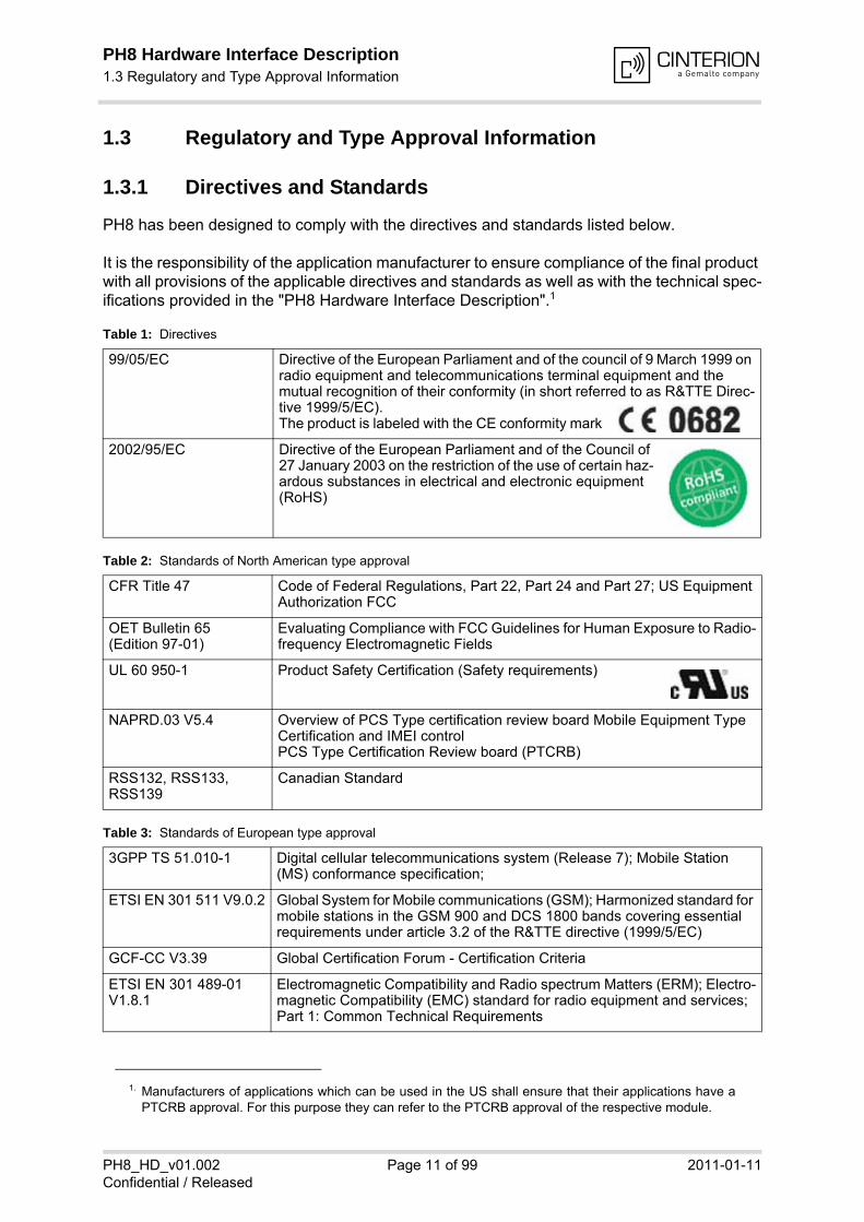
1.3 Regulatory and Type Approval Information
1.3.1 Directives and Standards
PH8 has been designed to comply with the directives and standards listed below.
It is the responsibility of the application manufacturer to ensure compliance of the final product with all provisions of the applicable directives and standards as well as with the technical spec-ifications provided in the "PH8 Hardware Interface Description".1
1. Manufacturers of applications which can be used in the US shall ensure that their applications have aPTCRB approval. For this purpose they can refer to the PTCRB approval of the respective module.
Table 1: Directives
99/05/EC Directive of the European Parliament and of the council of 9 March 1999 on radio equipment and telecommunications terminal equipment and the mutual recognition of their conformity (in short referred to as R&TTE Direc-tive 1999/5/EC).The product is labeled with the CE conformity mark
2002/95/EC Directive of the European Parliament and of the Council of 27 January 2003 on the restriction of the use of certain haz-ardous substances in electrical and electronic equipment (RoHS)
Table 2: Standards of North American type approval
CFR Title 47 Code of Federal Regulations, Part 22, Part 24 and Part 27; US Equipment Authorization FCC
OET Bulletin 65(Edition 97-01)
Evaluating Compliance with FCC Guidelines for Human Exposure to Radio-frequency Electromagnetic Fields
UL 60 950-1 Product Safety Certification (Safety requirements)
NAPRD.03 V5.4 Overview of PCS Type certification review board Mobile Equipment Type Certification and IMEI controlPCS Type Certification Review board (PTCRB)
RSS132, RSS133, RSS139
Canadian Standard
Table 3: Standards of European type approval
3GPP TS 51.010-1 Digital cellular telecommunications system (Release 7); Mobile Station (MS) conformance specification;
ETSI EN 301 511 V9.0.2 Global System for Mobile communications (GSM); Harmonized standard for mobile stations in the GSM 900 and DCS 1800 bands covering essential requirements under article 3.2 of the R&TTE directive (1999/5/EC)
GCF-CC V3.39 Global Certification Forum - Certification Criteria
ETSI EN 301 489-01 V1.8.1
Electromagnetic Compatibility and Radio spectrum Matters (ERM); Electro-magnetic Compatibility (EMC) standard for radio equipment and services; Part 1: Common Technical Requirements

PH8 Hardware Interface Description1.3 Regulatory and Type Approval Information16
PH8_HD_v01.002 Page 12 of 99 2011-01-11Confidential / Released
ETSI EN 301 489-07 V1.3.1
Electromagnetic Compatibility and Radio spectrum Matters (ERM); Electro-magnetic Compatibility (EMC) standard for radio equipment and services; Part 7: Specific conditions for mobile and portable radio and ancillary equip-ment of digital cellular radio telecommunications systems (GSM and DCS)
ETSI EN 301 489-24 V1.4.1
Electromagnetic Compatibility and Radio spectrum Matters (ERM); Electro-magnetic Compatibility (EMC) standard for radio equipment and services; Part 24: Specific conditions for IMT-2000 CDMA Direct Spread (UTRA) for Mobile and portable (UE) radio and ancillary equipment
EN 301 908-01 V3.2.1 Electromagnetic compatibility and Radio spectrum Matters (ERM); Base Stations (BS) and User Equipment (UE) for IMT-2000 Third Generation cel-lular networks; Part 1: Harmonized EN for IMT-2000, introduction and com-mon requirements of article 3.2 of the R&TTE Directive
EN 301 908-02 V3.2.1 Electromagnetic compatibility and Radio spectrum Matters (ERM); Base Stations (BS) and User Equipment (UE) for IMT-2000 Third Generation cel-lular networks; Part 2: Harmonized EN for IMT-2000, CDMA Direct Spread (UTRA FDD) (UE) covering essential requirements of article 3.2 of the R&TTE Directive
EN 62311:2008 Assessment of electronic and electrical equipment related to human expo-sure restrictions for electromagnetic fields (0 Hz - 300 GHz)
IEC/EN 60950-1:2006 Safety of information technology equipment
Table 4: Requirements of quality
IEC 60068 Environmental testing
DIN EN 60529 IP codes
Table 5: Standards of the Ministry of Information Industry of the People’s Republic of China
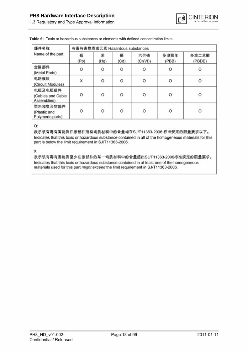
SJ/T 11363-2006 “Requirements for Concentration Limits for Certain Hazardous Substances in Electronic Information Products” (2006-06).
SJ/T 11364-2006 “Marking for Control of Pollution Caused by Electronic Information Products” (2006-06).
According to the “Chinese Administration on the Control of Pollution caused by Electronic Information Products” (ACPEIP) the EPUP, i.e., Environmental Protection Use Period, of this product is 20 years as per the symbol shown here, unless otherwise marked. The EPUP is valid only as long as the product is operated within the operating limits described in the Cinterion Hardware Interface Description.
Please see Table 6 for an overview of toxic or hazardous substances or ele-ments that might be contained in product parts in concentrations above the limits defined by SJ/T 11363-2006.
Table 3: Standards of European type approval
PH8 Hardware Interface Description1.3 Regulatory and Type Approval Information16
PH8_HD_v01.002 Page 13 of 99 2011-01-11Confidential / Released
Table 6: Toxic or hazardous substances or elements with defined concentration limits
PH8 Hardware Interface Description1.3 Regulatory and Type Approval Information16
PH8_HD_v01.002 Page 14 of 99 2011-01-11Confidential / Released
1.3.2 SAR requirements specific to portable mobiles
Mobile phones, PDAs or other portable transmitters and receivers incorporating a GSM module must be in accordance with the guidelines for human exposure to radio frequency energy. This requires the Specific Absorption Rate (SAR) of portable PH8 based applications to be evaluat-ed and approved for compliance with national and/or international regulations.
Since the SAR value varies significantly with the individual product design manufacturers are advised to submit their product for approval if designed for portable use. For European and US-markets the relevant directives are mentioned below. It is the responsibility of the manufacturer of the final product to verify whether or not further standards, recommendations or directives are in force outside these areas.
Products intended for sale on US marketsES 59005/ANSI C95.1 Considerations for evaluation of human exposure to electromagnetic
fields (EMFs) from mobile telecommunication equipment (MTE) in thefrequency range 30MHz - 6GHz
Products intended for sale on European marketsEN 50360 Product standard to demonstrate the compliance of mobile phones with
the basic restrictions related to human exposure to electromagneticfields (300MHz - 3GHz)
IMPORTANT:Manufacturers of portable applications based on PH8 modules are required to have their final product certified and apply for their own FCC Grant and Industry Canada Certificate related to the specific portable mobile. See also Section 9.2.
PH8 Hardware Interface Description1.3 Regulatory and Type Approval Information16
PH8_HD_v01.002 Page 15 of 99 2011-01-11Confidential / Released
1.3.3 SELV Requirements
The power supply connected to the PH8 module shall be in compliance with the SELV require-ments defined in EN 60950-1.
1.3.4 Safety Precautions
The following safety precautions must be observed during all phases of the operation, usage, service or repair of any cellular terminal or mobile incorporating PH8. Manufacturers of the cel-lular terminal are advised to convey the following safety information to users and operating per-sonnel and to incorporate these guidelines into all manuals supplied with the product. Failure to comply with these precautions violates safety standards of design, manufacture and intend-ed use of the product. Cinterion Wireless Modules assumes no liability for customer’s failure to comply with these precautions.
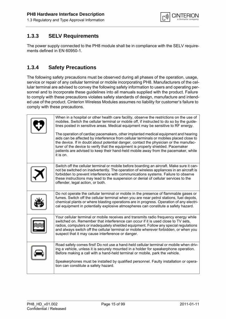
When in a hospital or other health care facility, observe the restrictions on the use of mobiles. Switch the cellular terminal or mobile off, if instructed to do so by the guide-lines posted in sensitive areas. Medical equipment may be sensitive to RF energy.
The operation of cardiac pacemakers, other implanted medical equipment and hearing aids can be affected by interference from cellular terminals or mobiles placed close to the device. If in doubt about potential danger, contact the physician or the manufac-turer of the device to verify that the equipment is properly shielded. Pacemaker patients are advised to keep their hand-held mobile away from the pacemaker, while it is on.
Switch off the cellular terminal or mobile before boarding an aircraft. Make sure it can-not be switched on inadvertently. The operation of wireless appliances in an aircraft is forbidden to prevent interference with communications systems. Failure to observe these instructions may lead to the suspension or denial of cellular services to the offender, legal action, or both.
Do not operate the cellular terminal or mobile in the presence of flammable gases or fumes. Switch off the cellular terminal when you are near petrol stations, fuel depots, chemical plants or where blasting operations are in progress. Operation of any electri-cal equipment in potentially explosive atmospheres can constitute a safety hazard.
Your cellular terminal or mobile receives and transmits radio frequency energy while switched on. Remember that interference can occur if it is used close to TV sets, radios, computers or inadequately shielded equipment. Follow any special regulations and always switch off the cellular terminal or mobile wherever forbidden, or when you suspect that it may cause interference or danger.
Road safety comes first! Do not use a hand-held cellular terminal or mobile when driv-ing a vehicle, unless it is securely mounted in a holder for speakerphone operation. Before making a call with a hand-held terminal or mobile, park the vehicle.
Speakerphones must be installed by qualified personnel. Faulty installation or opera-tion can constitute a safety hazard.
PH8 Hardware Interface Description1.3 Regulatory and Type Approval Information16
PH8_HD_v01.002 Page 16 of 99 2011-01-11Confidential / Released
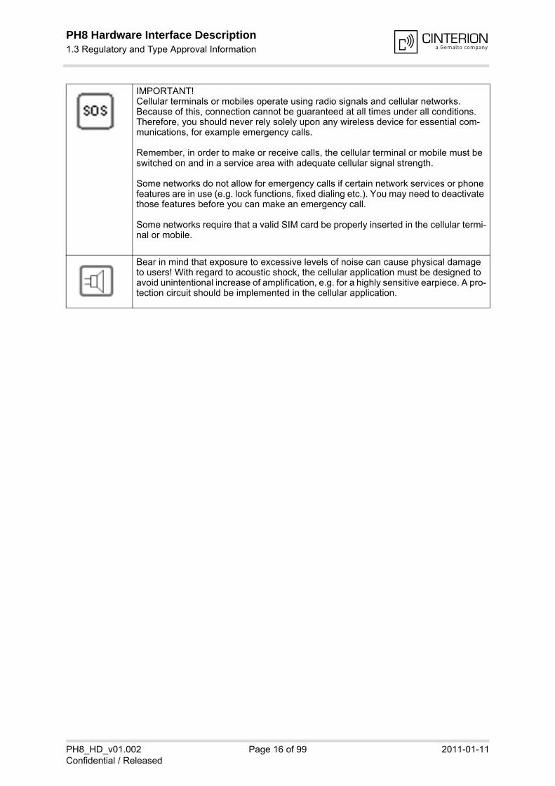
IMPORTANT!Cellular terminals or mobiles operate using radio signals and cellular networks. Because of this, connection cannot be guaranteed at all times under all conditions. Therefore, you should never rely solely upon any wireless device for essential com-munications, for example emergency calls.
Remember, in order to make or receive calls, the cellular terminal or mobile must be switched on and in a service area with adequate cellular signal strength.
Some networks do not allow for emergency calls if certain network services or phone features are in use (e.g. lock functions, fixed dialing etc.). You may need to deactivate those features before you can make an emergency call.
Some networks require that a valid SIM card be properly inserted in the cellular termi-nal or mobile.
Bear in mind that exposure to excessive levels of noise can cause physical damage to users! With regard to acoustic shock, the cellular application must be designed to avoid unintentional increase of amplification, e.g. for a highly sensitive earpiece. A pro-tection circuit should be implemented in the cellular application.

PH8 Hardware Interface Description2 Product Concept21
PH8_HD_v01.002 Page 17 of 99 2011-01-11Confidential / Released
2 Product Concept
2.1 Key Features at a Glance
Feature Implementation
General
Frequency bands GSM/GPRS/EDGE: Quad band, 850/900/1800/1900MHzUMTS/HSPA+: Five band, 800/850/AWS/1900/2100MHz
GSM class Small MS
Output power (according to Release 99)
Class 4 (+33dBm ±2dB) for EGSM850Class 4 (+33dBm ±2dB) for EGSM900Class 1 (+30dBm ±2dB) for GSM1800Class 1 (+30dBm ±2dB) for GSM1900Class E2 (+27dBm ± 3dB) for GSM 850 8-PSKClass E2 (+27dBm ± 3dB) for GSM 900 8-PSKClass E2 (+26dBm +3 /-4dB) for GSM 1800 8-PSKClass E2 (+26dBm +3 /-4dB) for GSM 1900 8-PSKClass 3 (+24dBm +1/-3dB) for UMTS 2100, WCDMA FDD BdIClass 3 (+24dBm +1/-3dB) for UMTS 1900,WCDMA FDD BdIIClass 3 (+24dBm +1/-3dB) for UMTS AWS, WCDMA FDD BdIVClass 3 (+24dBm +1/-3dB) for UMTS 850, WCDMA FDD BdVClass 3 (+24dBm +1/-3dB) for UMTS 800, WCDMA FDD BdVI
Power supply 3.3V < VBATT+ < 4.2V
Operating temperature (board temperature)
Normal operation: -30°C to +85°CRestricted operation: -40°C to +95°C
Physical Dimensions: 33.9mm x 50mm x 3.1mmWeight: approx. 9.5g
RoHS All hardware components fully compliant with EU RoHS Directive
HSPA features
3GPP Release 6, 7 DL 14.4Mbps, UL 5.7MbpsUE CAT. [1-6], 11, 12 supportedCompressed mode (CM) supported according to 3GPP TS25.212
UMTS features
3GPP Release 4 PS data rate – 384 kbps DL / 384 kbps ULCS data rate – 64 kbps DL / 64 kbps UL
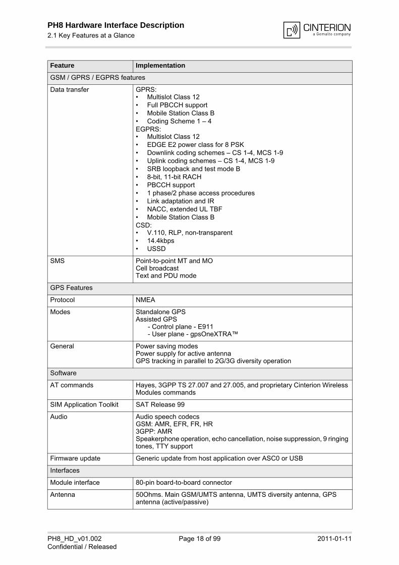
PH8 Hardware Interface Description2.1 Key Features at a Glance21
PH8_HD_v01.002 Page 18 of 99 2011-01-11Confidential / Released
GSM / GPRS / EGPRS features
Data transfer GPRS:• Multislot Class 12• Full PBCCH support• Mobile Station Class B• Coding Scheme 1 – 4EGPRS:• Multislot Class 12• EDGE E2 power class for 8 PSK• Downlink coding schemes – CS 1-4, MCS 1-9• Uplink coding schemes – CS 1-4, MCS 1-9• SRB loopback and test mode B• 8-bit, 11-bit RACH• PBCCH support• 1 phase/2 phase access procedures• Link adaptation and IR• NACC, extended UL TBF• Mobile Station Class BCSD:• V.110, RLP, non-transparent• 14.4kbps• USSD
SMS Point-to-point MT and MOCell broadcastText and PDU mode
GPS Features
Protocol NMEA
Modes Standalone GPSAssisted GPS
- Control plane - E911- User plane - gpsOneXTRA™
General Power saving modesPower supply for active antennaGPS tracking in parallel to 2G/3G diversity operation
Software
AT commands Hayes, 3GPP TS 27.007 and 27.005, and proprietary Cinterion Wireless Modules commands
SIM Application Toolkit SAT Release 99
Audio Audio speech codecsGSM: AMR, EFR, FR, HR3GPP: AMRSpeakerphone operation, echo cancellation, noise suppression, 9 ringing tones, TTY support
Firmware update Generic update from host application over ASC0 or USB
Interfaces
Module interface 80-pin board-to-board connector
Antenna 50Ohms. Main GSM/UMTS antenna, UMTS diversity antenna, GPS antenna (active/passive)
Feature Implementation

PH8 Hardware Interface Description2.1 Key Features at a Glance21
PH8_HD_v01.002 Page 19 of 99 2011-01-11Confidential / Released
USB USB 2.0 High Speed (480Mbit/s) or Full Speed (12Mbit/s) device inter-face
Serial interface ASC0:• 8-wire modem interface with status and control lines, unbalanced,
asynchronous• Adjustable baud rates from 9,600bps up to 921,600bps• Supports RTS0/CTS0 hardware flow control• Multiplex ability according to GSM 07.10 Multiplexer Protocol
UICC interface Supported chip cards: UICC/SIM/USIM 3V, 1.8V
Status Signal pin to indicate network connectivity state
Audio 1 analog interface with microphone feeding1 digital interface (PCM)
Power on/off, Reset
Power on/off Switch-on by hardware pin IGTSwitch-off by AT command (AT^SMSO)Automatic switch-off in case of critical temperature or voltage conditions.
Reset Orderly shutdown and reset by AT command
Emergency-off Emergency-off by hardware pin EMERG_OFF if IGT is not active.
Special Features
Phonebook SIM and phone
TTY/CTM support Integrated CTM modem
Antenna SAIC (Single Antenna Interference Cancellation) / DARP (Downlink Advanced Receiver Performance)RX diversity type 3i
Evaluation kit
DSB75 DSB75 Evaluation Board designed to test and type approve Cinterion Wireless Modules and provide a sample configuration for application engineering. A special adapter is required to connect the module to the DSB75.
Feature Implementation

PH8 Hardware Interface Description2.2 PH8 System Overview21
PH8_HD_v01.002 Page 20 of 99 2011-01-11Confidential / Released
2.2 PH8 System Overview
Figure 1: PH8 system overview
USBSerialASC0
UICCAnalogaudio
Powersupply RTC
IGT,Emergency Off
Net state/status
SIMcard
Host application
User application
Module
Application
or
GSM/UMTS antenna
Pow
er
for
appl
icat
ion
(VE
XT
)P
owe
r in
dica
tion
(PW
R_I
ND
)
Mo
dem
inte
rfa
ce
Digitalaudio
PCM codec
GSM/UMTSGPS
GPS antennaUMTS
diversity antenna
PH8 Hardware Interface Description2.3 Circuit Concept21
PH8_HD_v01.002 Page 21 of 99 2011-01-11Confidential / Released
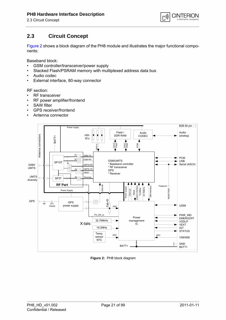
2.3 Circuit Concept
Figure 2 shows a block diagram of the PH8 module and illustrates the major functional compo-nents:
Baseband block:• GSM controller/transceiver/power supply• Stacked Flash/PSRAM memory with multiplexed address data bus• Audio codec• External interface, 80-way connector
RF section:• RF transceiver• RF power amplifier/frontend • SAW filter• GPS receiver/frontend• Antenna connector
Figure 2: PH8 block diagram
Power management
IC32.768kHz
Flash /DDR RAM
Audio(analog)
PCMUSBSerial (ASC0)
USIM
PWR_INDEMERGOFFVDDLPVEXTIGTSTATUS
VSENSE
GNDBATT+
19.2
MH
z
32.7
68k
Hz
19.2MHzX-tals:
AudioCODEC
Po
we
r su
ppl
y
Co
ntro
l in
terf
ace
Res
et
SIM
inte
rfac
e
Temp.sensor NTC
HW-ID’s
GP
IO’s
PC
M
D/A
/CF
lash
GPS power supply
GPS
GSM/UMTS
UMTSdiversity
Ant
enna
con
nect
ors
B2B 80 pin
GP
S R
F
GSM/UMTS* Baseband controller* RF transceiverGPS* Receiver
ADC
ADCFab
-ID
Power supply
Power Supply
ADC
BATT+
BA
TT
+
SP10T
SP3T
2x
3x
4x
3x
4x
GSM-TX
GSM-RX
UMTS-RX
UMTS-TX
Diversity
RF Part
HDET
RF DC-Supply
D/A
/CR
AM
Inte
rrup
t
PA_ON_xx
Testpoint:
RX
D0/
TX
D0

PH8 Hardware Interface Description3 Application Interface53
PH8_HD_v01.002 Page 22 of 99 2011-01-11Confidential / Released
3 Application Interface
PH8 is equipped with an 80-pin board-to-board connector that connects to the external appli-cation. The host interface incorporates several sub-interfaces described in the following sec-tions:
• Operating modes - see Section 3.1• Power supply - see Section 3.2• RTC backup - see Section 3.5• Serial interface USB - see Section 3.6• Serial interface ASC0 - Section 3.7• UICC/SIM/USIM interface - see Section 3.8• Analog audio interface - see Section 3.9• Pulse Code Modulation interface (PCM) - see Section 3.10• Status and control lines: IGT, EMERG_OFF, PWR_IND, STATUS - see Table 25

PH8 Hardware Interface Description3.1 Operating Modes53
PH8_HD_v01.002 Page 23 of 99 2011-01-11Confidential / Released
3.1 Operating Modes
The table below briefly summarizes the various operating modes referred to in the following chapters.
Table 7: Overview of operating modes
Mode Function
Normal operation
GSM / GPRS / UMTS / HSPA SLEEP
Power saving set automatically when no call is in progress and the USB connection is suspended by host or not present and no active commu-nication via ASC0.
GSM / GPRS / UMTS / HSPA IDLE
Power saving disabled (see [1]: AT^SCFG "MEopMode/PwrSave",<PwrSaveMode>) or an USB connection not suspended, but no call in progress.
GSM TALK/GSM DATA
Connection between two subscribers is in progress. Power consump-tion depends on the GSM network coverage and several connection settings (e.g. DTX off/on, FR/EFR/HR, hopping sequences and antenna connection). The following applies when power is to be mea-sured in TALK_GSM mode: DTX off, FR and no frequency hopping.
GPRS DATA GPRS data transfer in progress. Power consumption depends on net-work settings (e.g. power control level), uplink / downlink data rates and GPRS configuration (e.g. used multislot settings).
EGPRS DATA EGPRS data transfer in progress. Power consumption depends on net-work settings (e.g. power control level), uplink / downlink data rates and EGPRS configuration (e.g. used multislot settings).
UMTS TALK/UMTS DATA
UMTS data transfer in progress. Power consumption depends on net-work settings (e.g. TPC Pattern) and data transfer rate.
HSPA DATA HSPA data transfer in progress. Power consumption depends on net-work settings (e.g. TPC Pattern) and data transfer rate.
Power Down
Normal shutdown after sending the AT^SMSO command. Only a voltage regulator is active for powering the RTC. Software is not active. Interfaces are not accessible. Operating volt-age (connected to BATT+) remains applied.
Airplane mode
Airplane mode shuts down the radio part of the module, causes the module to log off from the GSM/GPRS network and disables all AT commands whose execution requires a radio connection.Airplane mode can be controlled by AT command (see [1]: AT^SCFG "MEopMode/Airplane"

PH8 Hardware Interface Description3.2 Power Supply53
PH8_HD_v01.002 Page 24 of 99 2011-01-11Confidential / Released
3.2 Power Supply
PH8 needs to be connected to a power supply at the board-to-board connector - 5 pins each BATT+ and GND. In addition, the VDDLP pin on the board-to-board connector may be connect-ed to an external capacitor or a battery to backup the RTC (see Section 3.5).
The power supply of PH8 has to be a single voltage source at BATT+. It must be able to provide the peak current during the uplink transmission.
All key functions for supplying power to the device are handled by the power management IC. It provides the following features:• Stabilizes the supply voltages for the baseband using switching regulators and low drop lin-
ear voltage regulators.• Switches the module's power voltages for the power-up and -down procedures.• Delivers, across the VEXT pin, a regulated voltage for an external application. This voltage
is not available in Power-down mode and can be reduced via AT command to save power(see Table 25: VEXT).
• SIM switch to provide SIM power supply.
3.2.1 Minimizing Power Losses
When designing the power supply for your application please pay specific attention to power losses. Ensure that the input voltage VBATT+ never drops below 3.3V on the PH8 board, not even in a transmit burst where current consumption can rise to typical peaks of 2A. It should be noted that PH8 switches off when exceeding these limits. Any voltage drops that may occur in a trans-mit burst should not exceed 400mV to ensure the expected RF performance in 2G networks.
The measurement network monitors outburst and inburst values. The drop is the difference of both values. The maximum drop (Dmax) since the last start of the module will be saved. In IDLE and SLEEP mode, the module switches off if the minimum battery voltage (VBATTmin) is reached.
Example: VImin = 3.3VDmax = 0.4V
VBATTmin = VImin + DmaxVBATTmin = 3.3V + 0.4V = 3.7V
The best approach to reducing voltage drops is to use a board-to-board connection as recom-mended, and a low impedance power source. The resistance of the power supply lines on the host board and of a battery pack should also be considered.
Note: If the application design requires an adapter cable between both board-to-board connec-tors, use a flex cable as short as possible in order to minimize power losses.

PH8 Hardware Interface Description3.2 Power Supply53
PH8_HD_v01.002 Page 25 of 99 2011-01-11Confidential / Released
Example:If the length of the flex cable reaches the maximum length of 100mm, this connection may cause, for example, a resistance of 30m in the BATT+ line and 30m in the GND line. As a result, a 2A transmit burst would add up to a total voltage drop of 120mV. Plus, if a battery pack is involved, further losses may occur due to the resistance across the battery lines and the in-ternal resistance of the battery including its protection circuit.
Figure 3: Power supply limits during transmit burst
3.2.2 Monitoring Power Supply by AT Command
To monitor the supply voltage you can use the AT^SBV command which returns the averaged value related to BATT+ and GND at the board-to-board connector.
The module continuously measures the voltage at intervals depending on the operating mode of the RF interface. The duration of measuring ranges from 0.5s in TALK/DATA mode to 50s when PH8 is in Limited Service (deregistered). The displayed voltage (in mV) is averaged over the last measuring period before the AT^SBV command was executed.

PH8 Hardware Interface Description3.3 Power-Up / Power-Down Scenarios53
PH8_HD_v01.002 Page 26 of 99 2011-01-11Confidential / Released
3.3 Power-Up / Power-Down Scenarios
In general, be sure not to turn on PH8 while it is beyond the safety limits of voltage and tem-perature stated in Section 6.1. PH8 would immediately switch off after having started and de-tected these inappropriate conditions. In extreme cases this can cause permanent damage to the module.
3.3.1 Turn on PH8
When the PH8 module is in Power-down mode, it can be started to Normal mode by driving the IGT (ignition) line to ground. it is recommended to use an open drain/collector driver to avoid current flowing into this pin. Pulling this pin low triggers a power-on sequence. To turn on PH8 IGT has to be kept active at least 100ms. After turning on PH8 IGT should be set inactive to prevent the module from turning on again after a shut down by AT command or EMERG_OFF.
Figure 4: Power-on with IGT
Note: After power up IGT should remain high.
Also note that with a USB connection the USB host may take more than 5 seconds to set up the virtual COM port connection.
BATT+
IGT
Power supplyactive
EMERG_OFF
Functionactive
PWR_IND
IGTPH8
Firmware start up, command interface initialization
ASC0
CTS0
USB*
Undefined state
Undefined state
Undefined state
0ms ~28ms ~5s
>100ms
Intermediate state
Intermediate state
* USB interface may take up to 5s to reach its active state (typ. 4s)
VEXT

PH8 Hardware Interface Description3.3 Power-Up / Power-Down Scenarios53
PH8_HD_v01.002 Page 27 of 99 2011-01-11Confidential / Released
3.3.2 Signal States after Startup
Table 8 describes the various states each interface signal passes through after startup and dur-ing operation.
Signals are in an undefined state while the module is initializing. Once the startup initialization has completed, i.e. when the software is running, all signals are in defined state. The state of several signals will change again once the respective interface is activated or configured by AT command.
Table 8: Signal states
Signal name Undefined state during startup Defined state after startup initialization
CCIN PU I, PU(100k)
CCRST PD O, L
CCIO PD O, L
CCCLK PD O, L
CCVCC Off 1.8V/2.85V
RXD0 I, PD O, H
TXD0 PD I, PD
CTS0 PD O, L1
1. Before reaching the defined state the signal has the intermediate state O, H for about 3s.
RTS0 PD I, PD
DTR0 PD I
DCD0 PU2
2. No external pull down allowed during this phase.
O, H
DSR0 PU O, L1
RING0 PU O, H
L = Low levelH = High levelI = InputO = Output
PD = Pull down with max. +30µAPD(…k) = Fix pull down resistorPU = Pull up with max. -30µAPU(…k) = Fix pull up resistor

PH8 Hardware Interface Description3.3 Power-Up / Power-Down Scenarios53
PH8_HD_v01.002 Page 28 of 99 2011-01-11Confidential / Released
3.3.3 Turn off PH8 Using AT Command
The best and safest approach to powering down PH8 is to issue the AT^SMSO command. This procedure lets PH8 log off from the network and allows the software to enter into a secure state and safe data before disconnecting the power supply. The mode is referred to as Power Down mode. In this mode, only the RTC stays active. After sending AT^SMSO do not enter any other AT commands. There are two ways to verify that the module turns off:• Wait for the ”OK” – response. It indicates that data has been stored non-volatile and that
the module turns off after about 1 second.• Also, you can monitor the PWR_IND pin. A high state of the PWR_IND pin definitely indi-
cates that the module is switched off.
Be sure not to disconnect the supply voltage VBATT+ before the module has been switched off and the PWR_IND signal has gone high. Otherwise you run the risk of losing data.
While PH8 is in Power-down mode the application interface is switched off and must not be fed from any other source. Therefore, your application must be designed to avoid any current flow into any digital pins of the application interface, especially of the serial interfaces. No special care is required for the USB interface which is protected from reverse current.
Figure 5: Signal states during turn-off procedure
Note 1: Depending on capacitance load from host application
Note 2: After module shutdown by means of AT command, please allow for a time period of at least 1s before restarting the module.
VEXT See note 1
PWR_IND
Digital outputs
Power down
Digital inputs driven by application
PH8 Hardware Interface Description3.3 Power-Up / Power-Down Scenarios53
PH8_HD_v01.002 Page 29 of 99 2011-01-11Confidential / Released
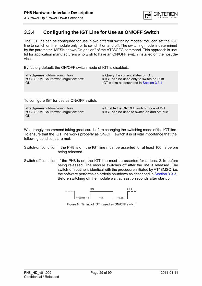
3.3.4 Configuring the IGT Line for Use as ON/OFF Switch
The IGT line can be configured for use in two different switching modes: You can set the IGT line to switch on the module only, or to switch it on and off. The switching mode is determined by the parameter "MEShutdown/OnIgnition" of the AT^SCFG command. This approach is use-ful for application manufacturers who wish to have an ON/OFF switch installed on the host de-vice.
By factory default, the ON/OFF switch mode of IGT is disabled::
To configure IGT for use as ON/OFF switch:
We strongly recommend taking great care before changing the switching mode of the IGT line. To ensure that the IGT line works properly as ON/OFF switch it is of vital importance that the following conditions are met.
Switch-on condition:If the PH8 is off, the IGT line must be asserted for at least 100ms beforebeing released.
Switch-off condition: If the PH8 is on, the IGT line must be asserted for at least 2.1s beforebeing released. The module switches off after the line is released. Theswitch-off routine is identical with the procedure initiated by AT^SMSO, i.e.the software performs an orderly shutdown as described in Section 3.3.3. Before switching off the module wait at least 5 seconds after startup.
Figure 6: Timing of IGT if used as ON/OFF switch
at^scfg=meshutdown/onignition^SCFG: "MEShutdown/OnIgnition","off"OK
# Query the current status of IGT.# IGT can be used only to switch on PH8.IGT works as described in Section 3.3.1.
at^scfg=meshutdown/onignition^SCFG: "MEShutdown/OnIgnition","on"OK
# Enable the ON/OFF switch mode of IGT.# IGT can be used to switch on and off PH8.
PH8 Hardware Interface Description3.3 Power-Up / Power-Down Scenarios53
PH8_HD_v01.002 Page 30 of 99 2011-01-11Confidential / Released
3.3.5 Automatic Shutdown
Automatic shutdown takes effect if:• The PH8 board is exceeding the critical limits of overtemperature or undertemperature• Undervoltage or overvoltage is detected
The automatic shutdown procedure is equivalent to the power down initiated with the AT^SMSO command, i.e. PH8 logs off from the network and the software enters a secure state avoiding loss of data.
Alert messages transmitted before the device switches off are implemented as Unsolicited Re-sult Codes (URCs). The presentation of the temperature URCs can be enabled or disabled with the AT commands AT^SCTM. The URC presentation mode varies with the condition, please see Section 3.3.5.1 to Section 3.3.5.3 for details. For further instructions on AT commands refer to [1].
PH8 Hardware Interface Description3.3 Power-Up / Power-Down Scenarios53
PH8_HD_v01.002 Page 31 of 99 2011-01-11Confidential / Released
3.3.5.1 Thermal Shutdown
The board temperature is constantly monitored by an internal NTC resistor located on the PCB. The values detected by the NTC resistor are measured directly on the board and therefore, are not fully identical with the ambient temperature.
Each time the board temperature goes out of range or back to normal, PH8 instantly displays an alert (if enabled).• URCs indicating the level "1" or "-1" allow the user to take appropriate precautions, such as
protecting the module from exposure to extreme conditions. The presentation of the URCsdepends on the settings selected with the AT^SCTM write command:AT^SCTM=1: Presentation of URCs is always enabled. AT^SCTM=0 (default): Presentation of URCs is enabled during the 15 second guard periodafter start-up of PH8. After expiry of the 15 second guard period, the presentation will bedisabled, i.e. no URCs with alert levels "1" or ''-1" will be generated.
• URCs indicating the level "2" or "-2" are instantly followed by an orderly shutdown. The pre-sentation of these URCs is always enabled, i.e. they will be output even though the factorysetting AT^SCTM=0 was never changed.
The maximum temperature ratings are stated in Section 6.2. Refer to Table 9 for the associated URCs.
The AT^SCTM command can also be used to check the present status of the board. Depending on the selected mode, the read command returns the current board temperature in degrees Celsius or only a value that indicates whether the board is within the safe or critical temperature range. See [1] for further instructions.
Table 9: Temperature dependent behavior
Sending temperature alert (15sec after PH8 start-up, otherwise only if URC presentation enabled)
^SCTM_B: 1 Caution: Board close to overtemperature limit, i.e., board is 5°C below overtem-perature limit.
^SCTM_B: -1 Caution: Board close to undertemperature limit, i.e., board is 5°C above under-temperature limit.
^SCTM_B: 0 Board back to uncritical temperature range, i.e., board is 6°C below its over- or above its undertemperature limit.
Automatic shutdown (URC appears no matter whether or not presentation was enabled)
^SCTM_B: 2 Alert: Board equal or beyond overtemperature limit. PH8 switches off.
^SCTM_B: -2 Alert: Board equal or below undertemperature limit. PH8 switches off.

PH8 Hardware Interface Description3.3 Power-Up / Power-Down Scenarios53
PH8_HD_v01.002 Page 32 of 99 2011-01-11Confidential / Released
3.3.5.2 Undervoltage Shutdown
If the measured battery voltage is no more sufficient to set up a call the following URC will be presented:
^SBC: Undervoltage.
The message will be reported, for example, when you attempt to make a call while the voltage is close to the shutdown threshold of VBATT+ and further power loss is caused during the transmit burst. In an idle state, the shutdown threshold is the sum of the module’s minimum supply volt-age (VBATT+) and the value of the maximum voltage drop resulting from earlier calls. This means that in an idle state the actual shutdown threshold may be higher than VBATT+. Therefore, to properly calculate the actual shutdown threshold application manufacturers are advised to measure the maximum voltage drops that may occur during transmit bursts.
This type of URC does not need to be activated by the user. It will be output automatically when fault conditions occur.
3.3.5.3 Overvoltage Shutdown
The overvoltage shutdown threshold is 100mV above the maximum supply voltage VBATT+ specified in Table 25.
When the supply voltage approaches the overvoltage shutdown threshold the module will send the following URC:
^SBC: Overvoltage warningThis alert is sent once.
When the overvoltage shutdown threshold is exceeded the module will send the following URC^SBC: Overvoltage shutdown
before it shuts down cleanly:
This type of URC does not need to be activated by the user. It will be output automatically when fault conditions occur.
Keep in mind that several PH8 components are directly linked to BATT+ and, therefore, the supply voltage remains applied at major parts of PH8, even if the module is switched off. Es-pecially the power amplifier is very sensitive to high voltage and might even be destroyed.

PH8 Hardware Interface Description3.3 Power-Up / Power-Down Scenarios53
PH8_HD_v01.002 Page 33 of 99 2011-01-11Confidential / Released
3.3.6 Turn off PH8 in Case of Emergency
Caution: Use the EMERG_OFF pin only when, due to serious problems, the software is not re-sponding for more than 5 seconds. Pulling the EMERG_OFF pin causes the loss of all informa-tion stored in the volatile memory. Therefore, this procedure is intended only for use in case of emergency, e.g. if PH8 does not respond, if reset or shutdown via AT command fails.
The EMERG_OFF line is available on the application interface and can be used to switch off the module. To control the EMERG_OFF line it is recommended to use an open drain / collector driver.
To switch off, the EMERG_OFF line must be pulled to ground for longer than 40ms. After the 40ms and an additional delay period of 500ms the module shuts down as shown in Figure 7.
Figure 7: Shutdown by EMERG_OFF signal
PWR_IND
EMERG_OFF
VEXT
>40ms
Shut Down
500ms40ms
PH8 Hardware Interface Description3.4 Power Saving53
PH8_HD_v01.002 Page 34 of 99 2011-01-11Confidential / Released
3.4 Power Saving
PH8 is able to reduce its functionality to a minimum (during the so-called SLEEP mode) in order to minimize its current consumption. The following sections explain the module’s network dependant power saving behavior and also mention how to wake up from or disble the so-called SLEEP mode.
The implementation of the USB host interface also influences the module’s power saving behavior and therefore its current consumption. For more information see Section 3.6.
Note. The module’s SLEEP mode current consumption can be reduced significantly by enabling the VEXT power save mode. Hence, it is recommended to enable power saving on VEXT if at all possible. For more information see Table 25: VEXT.
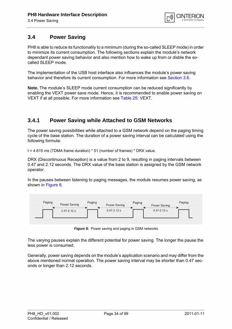
3.4.1 Power Saving while Attached to GSM Networks
The power saving possibilities while attached to a GSM network depend on the paging timing cycle of the base station. The duration of a power saving interval can be calculated using the following formula:
t = 4.615 ms (TDMA frame duration) * 51 (number of frames) * DRX value.
DRX (Discontinuous Reception) is a value from 2 to 9, resulting in paging intervals between 0.47 and 2.12 seconds. The DRX value of the base station is assigned by the GSM network operator.
In the pauses between listening to paging messages, the module resumes power saving, as shown in Figure 8.
Figure 8: Power saving and paging in GSM networks
The varying pauses explain the different potential for power saving. The longer the pause the less power is consumed.
Generally, power saving depends on the module’s application scenario and may differ from the above mentioned normal operation. The power saving interval may be shorter than 0.47 sec-onds or longer than 2.12 seconds.
PH8 Hardware Interface Description3.4 Power Saving53
PH8_HD_v01.002 Page 35 of 99 2011-01-11Confidential / Released
3.4.2 Power Saving while Attached to WCDMA Networks
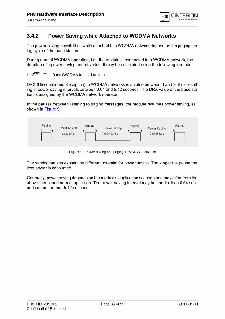
The power saving possibilities while attached to a WCDMA network depend on the paging tim-ing cycle of the base station.
During normal WCDMA operation, i.e., the module is connected to a WCDMA network, the duration of a power saving period varies. It may be calculated using the following formula:
t = 2DRX value * 10 ms (WCDMA frame duration).
DRX (Discontinuous Reception) in WCDMA networks is a value between 6 and 9, thus result-ing in power saving intervals between 0.64 and 5.12 seconds. The DRX value of the base sta-tion is assigned by the WCDMA network operator.
In the pauses between listening to paging messages, the module resumes power saving, as shown in Figure 9.
Figure 9: Power saving and paging in WCDMA networks
The varying pauses explain the different potential for power saving. The longer the pause the less power is consumed.
Generally, power saving depends on the module’s application scenario and may differ from the above mentioned normal operation. The power saving interval may be shorter than 0.64 sec-onds or longer than 5.12 seconds.
PH8 Hardware Interface Description3.4 Power Saving53
PH8_HD_v01.002 Page 36 of 99 2011-01-11Confidential / Released
3.4.3 Timing of the CTS0 Signal, GSM/WCDMA
As long as PH8 is operated via the ASC0 interface and not in power saving mode, the CTS0 line is always active. This means that while attached to a network the CTS0 signal will be tem-porarily active during each paging.
After a concluding activity on the serial interface ASC0 - and depending on the module’s other activities - it takes by default 5 seconds before CTS0 goes inactive (again) and power saving starts (as described in Section 3.4.1 and Section 3.4.2). The 5 second delay period can be con-figured using the AT^SCFG parameter "MEopMode/PwrSave", <PwrSaveDelay> (see [1]).
With regard to programming or using timeouts, the UART must take the varying CTS0 inactivity periods into account.
Note: Hardware handshaking is mandatory if employing PH8’s ASC0 interface with enabled power saving. Thus AT commands are only recognized by the module while CTS0 is active.
3.4.4 Wake up from or Disabling Power Saving
The RTS0 line can be used to wake up the module from its power saving SLEEP mode. RTS0 activation (high to low transition) may be employed to cut short pauses between listening to paging messages. Following an RTS toggle the module will return to SLEEP mode 5 seconds after the last character was sent over the interface. This default delay period can be configured using the AT^SCFG parameter "MEopMode/PwrSave", <PwrSaveDelay>.
If not regularly woken up from power saving (through network requirements or by means of RTS toggling as described above), the power save period recommended for the AT^SCFG pa-rameter "MEopMode/PwrSave", <PwrSavePeriod> ensures that the module regularly wakes up from its power saving state (SLEEP mode). It is recommended to configure a regular module wake up, especially if the radio interface is switched off (Airplane mode) and the module is con-nected via serial interface (i.e., AT^SDPORT=2) to an external application without direct ac-cess to its RTS0 line (e.g., an application using standard Windows/Linux serial device drivers).
The AT^SCFG parameter "MEopMode/PwrSave", <PwrSaveMode> can be used to disable power saving completely, i.e., the module will no longer enter SLEEP mode but remain in IDLE mode instead. Please note that if this setting is used to avoid implementing hardware hand-shaking on ASC0, it is mandatory to have RTS0 pulled down or left open (an internal pull down is available).
For more information on power saving and the appropriate AT^SCFG parameters to configure the power save behavior see [1].
PH8 Hardware Interface Description3.5 RTC Backup53
PH8_HD_v01.002 Page 37 of 99 2011-01-11Confidential / Released
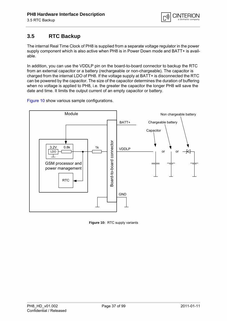
3.5 RTC Backup
The internal Real Time Clock of PH8 is supplied from a separate voltage regulator in the power supply component which is also active when PH8 is in Power Down mode and BATT+ is avail-able.
In addition, you can use the VDDLP pin on the board-to-board connector to backup the RTC from an external capacitor or a battery (rechargeable or non-chargeable). The capacitor is charged from the internal LDO of PH8. If the voltage supply at BATT+ is disconnected the RTC can be powered by the capacitor. The size of the capacitor determines the duration of buffering when no voltage is applied to PH8, i.e. the greater the capacitor the longer PH8 will save the date and time. It limits the output current of an empty capacitor or battery.
Figure 10 show various sample configurations.
Figure 10: RTC supply variants
Capacitor
Chargeable battery
Non chargeable battery
VDDLPor or
GSM processor and power management
RTC
Boa
rd-t
o-b
oard
con
nect
or
BATT+
Module
1k
GND
LDO
0.8k3.2V
PH8 Hardware Interface Description3.6 USB Interface53
PH8_HD_v01.002 Page 38 of 99 2011-01-11Confidential / Released
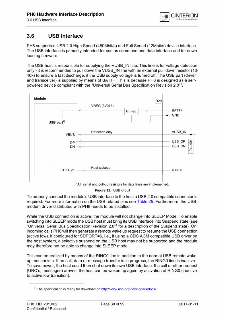
3.6 USB Interface
PH8 supports a USB 2.0 High Speed (480Mbit/s) and Full Speed (12Mbit/s) device interface. The USB interface is primarily intended for use as command and data interface and for down-loading firmware.
The USB host is responsible for supplying the VUSB_IN line. This line is for voltage detection only - it is recommended to pull down the VUSB_IN line with an external pull down resistor (10-40k) to ensure a fast discharge, if the USB supply voltage is turned off. The USB part (driver and transceiver) is supplied by means of BATT+. This is because PH8 is designed as a self-powered device compliant with the “Universal Serial Bus Specification Revision 2.0”1.
Figure 11: USB circuit
To properly connect the module's USB interface to the host a USB 2.0 compatible connector is required. For more information on the USB related pins see Table 25. Furthermore, the USB modem driver distributed with PH8 needs to be installed.
While the USB connection is active, the module will not change into SLEEP Mode. To enable switching into SLEEP mode the USB host must bring its USB interface into Suspend state (see “Universal Serial Bus Specification Revision 2.0“1 for a description of the Suspend state). On incoming calls PH8 will then generate a remote wake up request to resume the USB connection (active low). If configured for SDPORT=6, i.e., if using a CDC ACM compatible USB driver on the host system, a selective suspend on the USB host may not be supported and the module may therefore not be able to change into SLEEP mode.
This can be realized by means of the RING0 line in addition to the normal USB remote wake up mechanism. If no call, data or message transfer is in progress, the RING0 line is inactive. To save power, the host could then shut down its own USB interface. If a call or other request (URC’s, messages) arrives, the host can be woken up again by activation of RING0 (inactive to active low transition).
1. The specification is ready for download on http://www.usb.org/developers/docs/
VBUS
DPDN
VREG (3V075)
B2B
BATT+
USB_DP
lin. reg.GND
Module
Detection only VUSB_IN
USB part1)
RING0Host wakeup
GPIO_21
1) All serial and pull-up resistors for data lines are implemented.
USB_DN
10k.
..40
k
PH8 Hardware Interface Description3.7 Serial Interface ASC053
PH8_HD_v01.002 Page 39 of 99 2011-01-11Confidential / Released
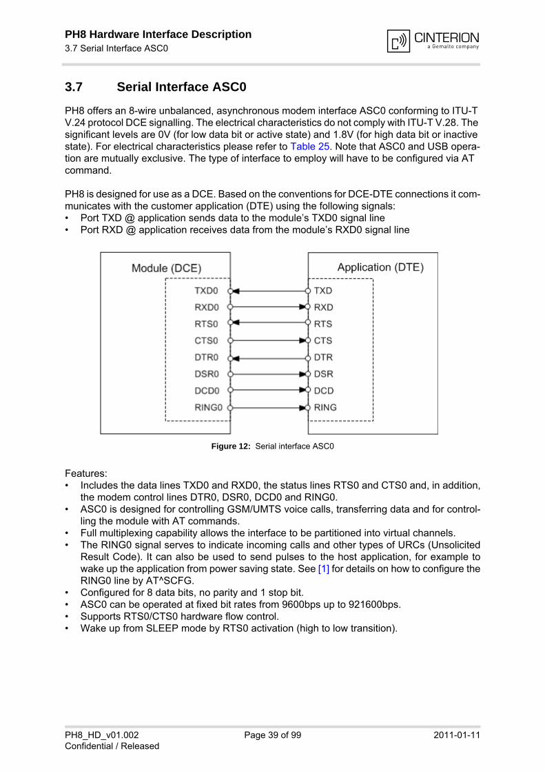
3.7 Serial Interface ASC0
PH8 offers an 8-wire unbalanced, asynchronous modem interface ASC0 conforming to ITU-T V.24 protocol DCE signalling. The electrical characteristics do not comply with ITU-T V.28. The significant levels are 0V (for low data bit or active state) and 1.8V (for high data bit or inactive state). For electrical characteristics please refer to Table 25. Note that ASC0 and USB opera-tion are mutually exclusive. The type of interface to employ will have to be configured via AT command.
PH8 is designed for use as a DCE. Based on the conventions for DCE-DTE connections it com-municates with the customer application (DTE) using the following signals:• Port TXD @ application sends data to the module’s TXD0 signal line• Port RXD @ application receives data from the module’s RXD0 signal line
Figure 12: Serial interface ASC0
Features:• Includes the data lines TXD0 and RXD0, the status lines RTS0 and CTS0 and, in addition,
the modem control lines DTR0, DSR0, DCD0 and RING0.• ASC0 is designed for controlling GSM/UMTS voice calls, transferring data and for control-
ling the module with AT commands.• Full multiplexing capability allows the interface to be partitioned into virtual channels.• The RING0 signal serves to indicate incoming calls and other types of URCs (Unsolicited
Result Code). It can also be used to send pulses to the host application, for example towake up the application from power saving state. See [1] for details on how to configure theRING0 line by AT^SCFG.
• Configured for 8 data bits, no parity and 1 stop bit. • ASC0 can be operated at fixed bit rates from 9600bps up to 921600bps.• Supports RTS0/CTS0 hardware flow control.• Wake up from SLEEP mode by RTS0 activation (high to low transition).

PH8 Hardware Interface Description3.7 Serial Interface ASC053
PH8_HD_v01.002 Page 40 of 99 2011-01-11Confidential / Released
Table 10: DCE-DTE wiring of ASC0
V.24 circuit DCE DTE
Line function Signal direction Line function Signal direction
103 TXD0 Input TXD Output
104 RXD0 Output RXD Input
105 RTS0 Input RTS Output
106 CTS0 Output CTS Input
108/2 DTR0 Input DTR Output
107 DSR0 Output DSR Input
109 DCD0 Output DCD Input
125 RING0 Output RING Input
PH8 Hardware Interface Description3.8 UICC/SIM/USIM Interface53
PH8_HD_v01.002 Page 41 of 99 2011-01-11Confidential / Released
3.8 UICC/SIM/USIM Interface
PH8 has an integrated UICC/SIM/USIM interface compatible with the 3GPP 31.102 and ETSI 102 221. This is wired to the host interface (board-to-board connector) in order to be connected to an external SIM card holder. Six pins on the board-to-board connector are reserved for the SIM interface.
The UICC/SIM/USIM interface supports 3V and 1.8V SIM cards. Please refer to Table 25 for electrical specifications of the UICC/SIM/USIM interface lines depending on whether a 3V or 1.8V SIM card is used.
The CCIN pin serves to detect whether a tray (with SIM card) is present in the card holder. Us-ing the CCIN pin is mandatory for compliance with the GSM 11.11 recommendation if the me-chanical design of the host application allows the user to remove the SIM card during operation. To take advantage of this feature, an appropriate SIM card detect switch is required on the card holder. For example, this is true for the model supplied by Molex, which has been tested to op-erate with PH8 and is part of the Cinterion reference equipment submitted for type approval. See Chapter 10 for Molex ordering numbers.
Note: No guarantee can be given, nor any liability accepted, if loss of data is encountered after removing the SIM card during operation. Also, no guarantee can be given for properly initializ-ing any SIM card that the user inserts after having removed the SIM card during operation. In this case, the application must restart PH8.
Table 11: Signals of the SIM interface (board-to-board connector)
Signal Description
CCGND Separate ground connection for SIM card to improve EMC.Be sure to use this ground line for the SIM interface rather than any other ground pin or plane on the module.
CCCLK Chipcard clock
CCVCC SIM supply voltage.
CCIO Serial data line, input and output.
CCRST Chipcard reset
CCIN Input on the baseband processor for detecting a SIM card tray in the holder. If the SIM is removed during operation the SIM interface is shut down immediately to prevent destruc-tion of the SIM. The CCIN pin is active low.The CCIN pin is mandatory for applications that allow the user to remove the SIM card dur-ing operation. The CCIN pin is solely intended for use with a SIM card. It must not be used for any other purposes. Failure to comply with this requirement may invalidate the type approval of PH8.

PH8 Hardware Interface Description3.8 UICC/SIM/USIM Interface53
PH8_HD_v01.002 Page 42 of 99 2011-01-11Confidential / Released
Figure 13: UICC/SIM/USIM interface
The total cable length between the board-to-board connector pins on PH8 and the pins of the external SIM card holder must not exceed 100mm in order to meet the specifications of 3GPP TS 51.010-1 and to satisfy the requirements of EMC compliance.
To avoid possible cross-talk from the CCCLK signal to the CCIO signal be careful that both lines are not placed closely next to each other. A useful approach is using the CCGND line to shield the CCIO line from the CCCLK line.
Module
open: Card removedclosed: Card inserted
CCRST
CCVCC
CCIO
CCCLK
CCIN
SIM /UICC1n
220n
Bo
ard
-to
-bo
ard
co
nn
ecto
r
CCGND
PH8 Hardware Interface Description3.9 Analog Audio Interface53
PH8_HD_v01.002 Page 43 of 99 2011-01-11Confidential / Released
3.9 Analog Audio Interface
PH8 has an analog audio interface with a balanced analog microphone input and a balanced analog earpiece output. A supply voltage and an analog ground connection are provided at dedicated pins.
PH8 offers six audio modes which can be selected with the AT^SNFS command. The electrical characteristics of the voiceband part vary with the audio mode. For example, sending and re-ceiving amplification, sidetone paths, noise suppression etc. depend on the selected mode and can in parts be altered with AT commands (except for mode 1).
Please refer to Section 6.7 for specifications of the audio interface and an overview of the audio parameters. Detailed instructions on using AT commands are presented in [1]. Table 28 sum-marizes the characteristics of the various audio modes and shows what parameters are sup-ported in each mode.
When shipped from factory, all audio parameters of PH8 are set to audio mode 1. This is the default configuration optimised for the Votronic HH-SI-30.3/V1.1/0 handset and used for type approving the Cinterion Wireless Modules reference configuration. Audio mode 1 has fix pa-rameters which cannot be modified. To adjust the settings of the Votronic handset simply change to another audio mode.

PH8 Hardware Interface Description3.9 Analog Audio Interface53
PH8_HD_v01.002 Page 44 of 99 2011-01-11Confidential / Released
3.9.1 Microphone Inputs and Supply
The differential microphone inputs MICP and MICN present variable impedances depending on the gain. The microphone inputs must be decoupled by capacitors Ck (typical 1µF). The in-put stage uses a differential operational amplifier circuit with programmable resistors in the in-put and the feedback path. The detailed structure of this stage and the following uplink path is shown in Figure 14. The input can be controlled by the AT command AT^SNFI. Command pa-rameters with their effect are mentioned the figure and marked in <red>. More information about audio AT commands can be found in Section 6.7 and [1].
Figure 14: Structure of Audio Input and Supply
MICP leads the signal via a resistor R1b to the non-inverting input of the operational amplifier which is then connected via a resistor R2b to VREF. The inverted signal goes through MICN via a feedback path of resistors R1a and R2a to the inverting input of the opamp. The gain of the first input stage can be programmed by the parameter <micAmp2>, in steps of 0.75dB and between -12dB and +35.25dB. R1a and R2a respective R1b and R2b are varied depending on this gain. The sum of R1a and R2a (respective R1b and R2b) is always 94kOhm. The value of R1a or R1b varies as listed in Table 12 for selected gains:
PH 8 Module
-
+
VREF
A
D
MICN
MICP
AGND
VREF
GND
AGND
VMIC
AGND
VMIC
0dB or 20dB
R2a
R1b
R1a
R2b
R1a + R2a = 94kR1b + R2b = 94k
Application GND
GND Line leading GSM burst current
GND
VGSM Noise
Connection Resistance
Ck
Ck
Rs
Rs
UL PCM
<micAmp2>
<micAmp1>
X
<micTxVol>
R1a = R1bR2a = R2b

PH8 Hardware Interface Description3.9 Analog Audio Interface53
PH8_HD_v01.002 Page 45 of 99 2011-01-11Confidential / Released
MICP presents a constant impedance of 94kOhm with respect to AGND. If MICP is AC coupled held at AGND, the impedance of MICN with respect to AGND is R1a (see Table 12). A floating differential source sees an impedance of R1a + R1b. The common mode input impedance is constantly 94kOhm for each input.
The matching of these resistors has an accuracy of 0.1% resulting in a maximum common mode rejection ratio of 60dB. The typical value is around 54dB.
A second gain stage follows that can be set to 0dB or 20dB using <micAmp1>. If 20dB is spec-ified, the common mode rejection ratio is reduced accordingly.
Finally, the uplink gain can be scaled in the PCM path by the <micTxVol> parameter.
It is recommended to use the AGND line for grounding the microphone circuit. AGND provides for the same module ground potential the analog circuits of the module refer to. AGND must not be connected to the system GND anywhere. Otherwise high GSM burst peak currents will flow across AGND causing GSM humming in the uplink audio signal.
A regulated power supply for electret microphones is available at VMIC. The voltage at VMIC is rated at 2.7V at 3mA and is available while audio is active (e.g., during a call).
Table 12: Feedback resistor values versus input gain
Gain [dB] R1a or R1b [kOhm] R2a or R2b [kOhm]
35.25 1.6 R2x = 94kOhm - R1x
30 2.9
18 11
12 19
6 31
0 47
-12 75

PH8 Hardware Interface Description3.9 Analog Audio Interface53
PH8_HD_v01.002 Page 46 of 99 2011-01-11Confidential / Released
The following figures show possible microphone and line connections.
Figure 15: Single ended microphone connection
The configuration shown in Figure 15 is suitable for short distances between microphone and module. A typical electret microphone has a metal case connected to its ground pad. Since this is routed directly to AGND, electro static discharges applied to the microphone will be easily led away. It is recommended to use an additional RC-filter for VMIC (for example 470 Ohm and 10µF as shown in the figure) in case a high microphone gain is necessary.
If the microphone lines are longer, use the configuration shown in Figure 16. It is recommended to use an additional RC-filter for VMIC (for example 1kOhm, 10µF and 1kOhm as shown in the figure) in case a high microphone gain is necessary.
Figure 16: Differential microphone connection
Module
AGND
VMIC
MICP
MICN
2k22k2
470
+
10µF
5k6
1µF
1µF
Module
AGND
MICP
MICN
1k
1k
1k
+10µF
1k
1µF
1µF
VMIC

PH8 Hardware Interface Description3.9 Analog Audio Interface53
PH8_HD_v01.002 Page 47 of 99 2011-01-11Confidential / Released
Figure 17: Line input
Using the line input configuration the output level of the ground related balanced source should be as high as possible to achieve the best SNR. Since the input impedance of PH8 is quite high at low gains, the coupling capacitances may be smaller.
3.9.2 Loudspeaker Output
PH8 provides a differential loudspeaker output EPP/EPN. If it is used as line output, the appli-cation should provide a capacitor decoupled differential input to eliminate GSM humming. A single ended connection to a speaker or a line input is strongly not recommended.
The following figures show the typical output configurations.
Figure 18: Differential loudspeaker connection
Figure 19: Line output connection
Module
MICN
100nF
MICP100nFLine output device
-1
~
Module
EPN
EPP
Module
EPN
EPP
+_
PH8 Hardware Interface Description3.10 Pulse Code Modulation Interface (PCM)53
PH8_HD_v01.002 Page 48 of 99 2011-01-11Confidential / Released
3.10 Pulse Code Modulation Interface (PCM)
PH8’s PCM interface can be used to connect audio devices capable of pulse code modulation. The PCM functionality allows the use of a codec like the Freescale MC145483. Using the AT^SAIC command you can activate and configure the PCM interface (see [1]).
The PCM interface supports the following modes:• Master mode, slave mode• Short frame synchronization• 256kHz, 512kHz and 2048kHz bit clock synchronization• Additional master mode with 128kHz, long frame synchronization
For the PCM interface configuration the parameters <clock>, <mode> <frame_mode> and <ext_clk_mode> of the AT^SAIC command can be configured. The following table lists possi-ble combinations:
In slave mode <clock> must be set according the source clock frequency. Being in master mode clock and frame synchronization signals may be permanently switched on by <ext_clk_mode> parameter. These signals may be used for clocking digital audio periphery outside a call.
Table 14 shows the assignment of the board-to-board pins to the PCM interface signals.
Table 13: Configuration combinations for the PCM interface
Configuration <clock> <mode> <frame_mode> <ext_clk_mode>
Master, 128kHz, long frame 0 0 1 0 or 1
Master, 256kHz, short frame 1 0 0 0 or 1
Master, 512kHz, short frame 2 0 0 0 or 1
Master, 2048kHz, short frame 3 0 0 0 or 1
Slave, 256kHz, short frame 1 1 0 1
Slave, 512kHz, short frame 2 1 0 1
Slave, 2048kHz, short frame 3 1 0 1
Table 14: Overview of PCM pin functions
Signal name on B2B connector
Signal direction: Master
Signal direction: Slave
Description
PCM_OUT (pin 26) O O PCM Data from PH8 to external codec
PCM_IN (pin 25) I I PCM Data from external codec to PH8
PCM_FSC (pin 24) O I Frame synchronization signal to/from external codec
PCM_CLK (pin 23) O I Bit clock to/from external codec

PH8 Hardware Interface Description3.10 Pulse Code Modulation Interface (PCM)53
PH8_HD_v01.002 Page 49 of 99 2011-01-11Confidential / Released
The timing of a PCM short frame is shown in Figure 20. The timing for master and slave mode is identical, except for the PCM_FSC and PCM_CLK signal direction (see Table 14).
Figure 20: PCM timing short frame (master/slave, 256, 512 or 2048KHz)
The timing of a PCM long frame for the additional 128kHz master mode is shown in Figure 21.
Figure 21: PCM timing long frame (master, 128kHz)
Please note that PCM data is always formatted as 16-bit uncompressed two’s complement. Al-so, all PCM data and frame synchronization signals are written to the PCM bus on the rising clock edge and read on the falling edge.
MSB
MSB
LSB
LSB
14 13
14 13
1
1
12
12
2
2
MSB
MSB
125 µs
PCM_FSC
PCM_OUT
PCM_IN
PCM_CLK
PCM_FSC
MSB
MSB
LSB
LSB
14 13
14 13
1
1
8
8
2
2
LSB1
1 LSB
MSB 14
MSB 14
7
7
PCM_OUT
PCM_IN
PCM_CLK
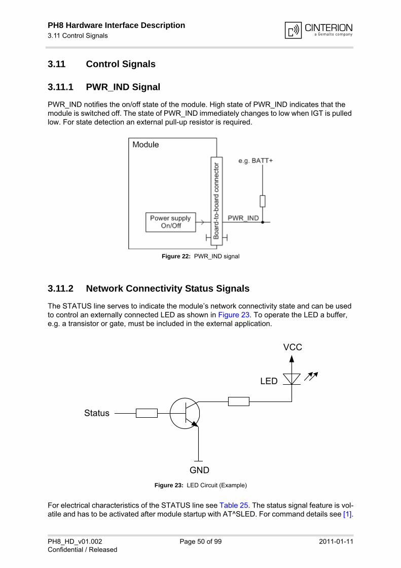
PH8 Hardware Interface Description3.11 Control Signals53
PH8_HD_v01.002 Page 50 of 99 2011-01-11Confidential / Released
3.11 Control Signals
3.11.1 PWR_IND Signal
PWR_IND notifies the on/off state of the module. High state of PWR_IND indicates that the module is switched off. The state of PWR_IND immediately changes to low when IGT is pulled low. For state detection an external pull-up resistor is required.
Figure 22: PWR_IND signal
3.11.2 Network Connectivity Status Signals
The STATUS line serves to indicate the module’s network connectivity state and can be used to control an externally connected LED as shown in Figure 23. To operate the LED a buffer, e.g. a transistor or gate, must be included in the external application.
Figure 23: LED Circuit (Example)
For electrical characteristics of the STATUS line see Table 25. The status signal feature is vol-atile and has to be activated after module startup with AT^SLED. For command details see [1].
VCC
Status
LED
GND

PH8 Hardware Interface Description3.11 Control Signals53
PH8_HD_v01.002 Page 51 of 99 2011-01-11Confidential / Released
3.11.3 Behavior of the RING0 Line (ASC0 Interface only)
The RING0 line is available on the first serial interface ASC0 (see also Section 3.7). The signal serves to indicate incoming calls and other types of URCs (Unsolicited Result Code).
Although not mandatory for use in a host application, it is strongly suggested that you connect the RING0 line to an interrupt line of your application. In this case, the application can be de-signed to receive an interrupt when a falling edge on RING0 occurs. This solution is most ef-fective, particularly, for waking up an application from power saving. Note that if the RING0 line is not wired, the application would be required to permanently poll the data and status lines of the serial interface at the expense of a higher current consumption. Therefore, utilizing the RING0 line provides an option to significantly reduce the overall current consumption of your application.
When a voice call comes in the RING0 line goes low (active) for 5.9s and high (inactive) for 0.1s. Every 6 seconds the ring string is generated and sent over the RXD0 line.
Figure 24: Incoming voice call
When a data call comes in the RING0 line goes low (active) for 0.1s and high (inactive) for 5.9s. Every 6 seconds the ring string is generated and sent over the RXD0 line.
Figure 25: Incoming data call
If there is a call in progress and call waiting is activated for a connected handset or handsfree device, the RING0 line switches to ground in order to generate acoustic signals that indicate the waiting call.
0.1s
RING0
0.1s
5.9s 5.9s 5.9sRing string
Ring string
Ring string
0.1s
RING00.1s
5.9s 5.9s 5.9s
Ring string
Ring string
Ring string
0.1s
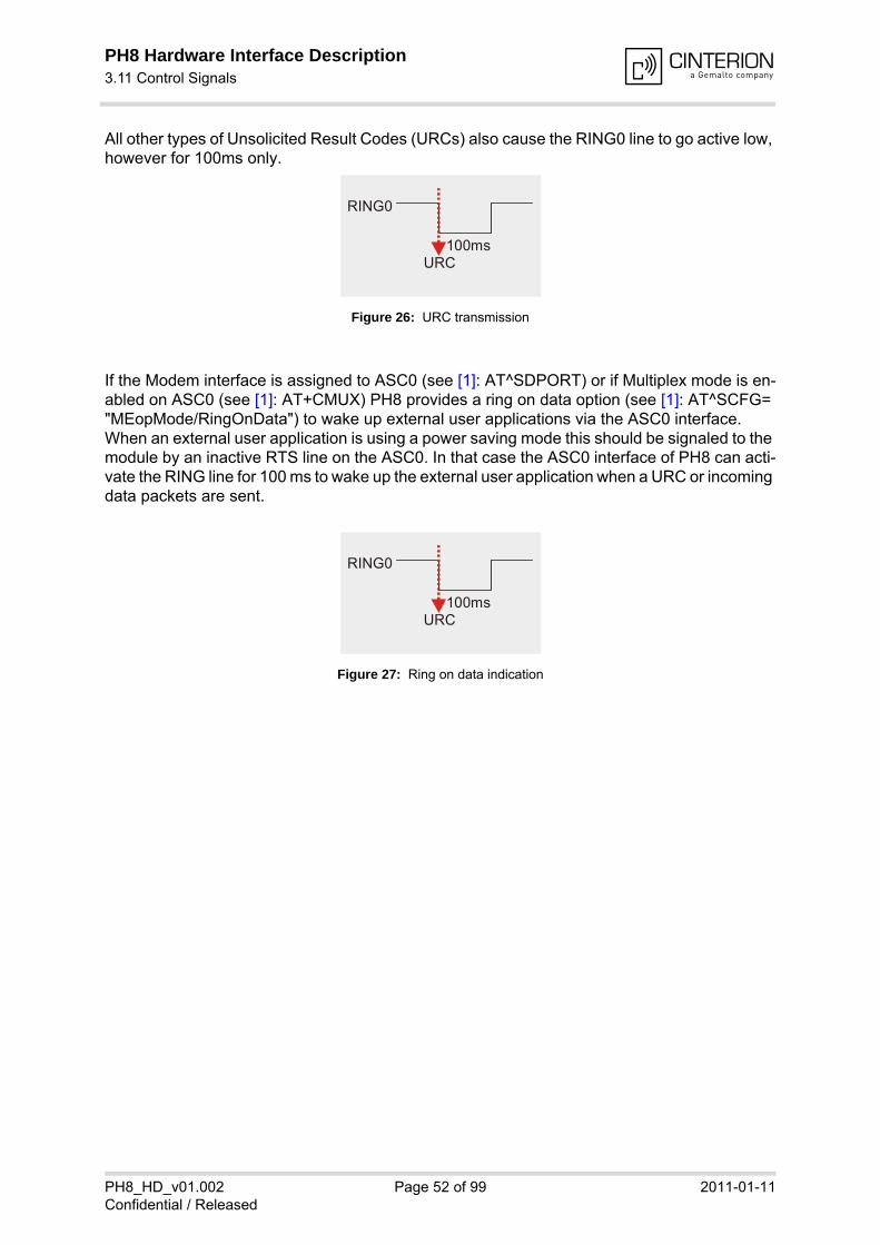
PH8 Hardware Interface Description3.11 Control Signals53
PH8_HD_v01.002 Page 52 of 99 2011-01-11Confidential / Released
All other types of Unsolicited Result Codes (URCs) also cause the RING0 line to go active low, however for 100ms only.
Figure 26: URC transmission
If the Modem interface is assigned to ASC0 (see [1]: AT^SDPORT) or if Multiplex mode is en-abled on ASC0 (see [1]: AT+CMUX) PH8 provides a ring on data option (see [1]: AT^SCFG= "MEopMode/RingOnData") to wake up external user applications via the ASC0 interface. When an external user application is using a power saving mode this should be signaled to the module by an inactive RTS line on the ASC0. In that case the ASC0 interface of PH8 can acti-vate the RING line for 100 ms to wake up the external user application when a URC or incoming data packets are sent.
Figure 27: Ring on data indication
100ms
RING0
URC
100ms
RING0
URC
PH8 Hardware Interface Description4 GPS Receiver53
PH8_HD_v01.002 Page 53 of 99 2011-01-11Confidential / Released
4 GPS Receiver
PH8 integrates a GPS receiver that offers the full performance of GPS technology. The GPS receiver is able to continuously track all satellites in view, thus providing accurate satellite posi-tion data.
The integrated GPS receiver supports the NMEA protocol via USB or ASC0 interface. NMEA is a combined electrical and data specification for communication between various (marine) electronic devices including GPS receivers. It has been defined and controlled by the US-based National Marine Electronics Association. For more information on the NMEA Standard please refer to http://www.nmea.org.
Depending on the receiver’s knowledge of last position, current time and ephemeris data, the receiver’s startup time (i.e., TTFF = Time-To-First-Fix) may vary: If the receiver has no knowl-edge of its last position or time, a startup takes considerably longer than if the receiver has still knowledge of its last position, time and almanac or has still access to valid ephimeris data and the precise time. For more information see Section 6.9.
By default, the GPS receiver is switched off. It has to be switched on and configured using AT commands. For more information on how to control the GPS interface via the AT commands AT^SGPSS and AT^SGPSC see [1].

PH8 Hardware Interface Description5 Antenna Interfaces59
PH8_HD_v01.002 Page 54 of 99 2011-01-11Confidential / Released
5 Antenna Interfaces
5.1 GSM/UMTS Antenna Interface
The PH8 GSM/UMTS antenna interface comprises a main GSM/UMTS antenna as well as an optional UMTS Rx diversity antenna to improve signal reliability and quality1. The interface has an impedance of 50Ω. PH8 is capable of sustaining a total mismatch at the antenna interface without any damage, even when transmitting at maximum RF power.
The external antenna must be matched properly to achieve best performance regarding radi-ated power, DC-power consumption, modulation accuracy and harmonic suppression. Match-ing networks are not included on the PH8 PCB and should be placed in the host application, if the antenna does not have an impendance of 50Ω.
Regarding the return loss PH8 provides the following values in the active band:
The connection of the antenna or other equipment must be decoupled from DC voltage. This is necessary because the antenna connector is DC coupled to ground via an inductor for ESD protection.
5.1.1 Antenna Installation
The U.FL antenna connector from Hirose/Molex of the main GSM/UMTS antenna has been chosen as antenna reference point (ARP) for the Cinterion Wireless Modules reference equip-ment submitted to type approve PH8. See Section 5.1.2 for details. All RF data specified throughout this manual is related to the ARP. The positions of the module’s antenna connectors can be seen in Figure 34.
1. By delivery default the optional UMTS Rx diversity antenna is configured as available for the module.Please refer to [1] for details on how to configure antenna settings.
Table 15: Return loss in the active band
State of module Return loss of module Recommended return loss of application
Receive > 8dB > 12dB
Transmit not applicable > 12dB
Idle < 5dB not applicable

PH8 Hardware Interface Description5.1 GSM/UMTS Antenna Interface59
PH8_HD_v01.002 Page 55 of 99 2011-01-11Confidential / Released
5.1.2 Antenna Connector
PH8 uses either an ultra-miniature SMT antenna connector from Hirose Ltd: U.FL-R-SMT, or the Molex 07341201 U.FL antenna connector. Both connectors have identical mechanical di-mensions (see Figure 28). Minor differences in product specifications are mentioned in Table 16. The position of the antenna connectors on the PH8 board can be seen in Figure 34.
Figure 28: Mechanical dimensions of PH8 antenna connectors
Table 16: Product specifications of PH8 antenna connectors
Item Specification Conditions
Ratings
Nominal impedance 50 Operating temp:-40°C to + 90°COperating humidity: max. 90%
Rated frequency DC to 3GHz
Mechanical characteristics
Repetitive operation Contact resistance:Center 25m Outside 15m
30 cycles of insertion and disen-gagement
Vibration No momentary disconnections of 1µs.No damage, cracks and looseness of parts.
Frequency of 10 to 100Hz, single amplitude of 1.5mm, acceleration of 59m/s2, for 5 cycles in the direc-tion of each of the 3 axes
Shock No momentary disconnections of 1µs.No damage, cracks and looseness of parts.
Acceleration of 735m/s2, 11ms duration for 6 cycles in the direc-tion of each of the 3 axes
Environmental characteristics
Humidity resistance No damage, cracks and looseness of parts.Insulation resistance: 100M min. at high humidity500M min. when dry
Exposure to 40°C, humidity of 95% for a total of 96 hours
Temperature cycle No damage, cracks and looseness of parts.Contact resistance:Center 25m Outside 15m
Temperature: +40°C 5 to 35°C +90°C 5 to 35°CTime: 30min within 5min 30min within 5min
Salt spray test No excessive corrosion 48 hours continuous exposure to 5% salt water

PH8 Hardware Interface Description5.1 GSM/UMTS Antenna Interface59
PH8_HD_v01.002 Page 56 of 99 2011-01-11Confidential / Released
Mating plugs and cables can be chosen from the Hirose U.FL Series or from other antenna equipment manufacturers like Molex or IMS. Examples from the Hirose U.FL Series are shown below and listed in Table 18. For latest product information please contact your respective an-tenna equipment manufacturer.
Figure 29: U.FL-R-SMT connector with U.FL-LP-040 plug
Figure 30: U.FL-R-SMT connector with U.FL-LP-066 plug
Table 17: Material and finish of PH8 antenna connectors and recommended plugs
Part Material Finish
Shell Phosphor bronze Hirose: Silver platingMolex: Gold plating
Male center contact Brass Gold plating
Female center contact Phosphor bronze Gold plating
Insulator Receptacle: LCP Hirose: Beige, Molex: Ivory
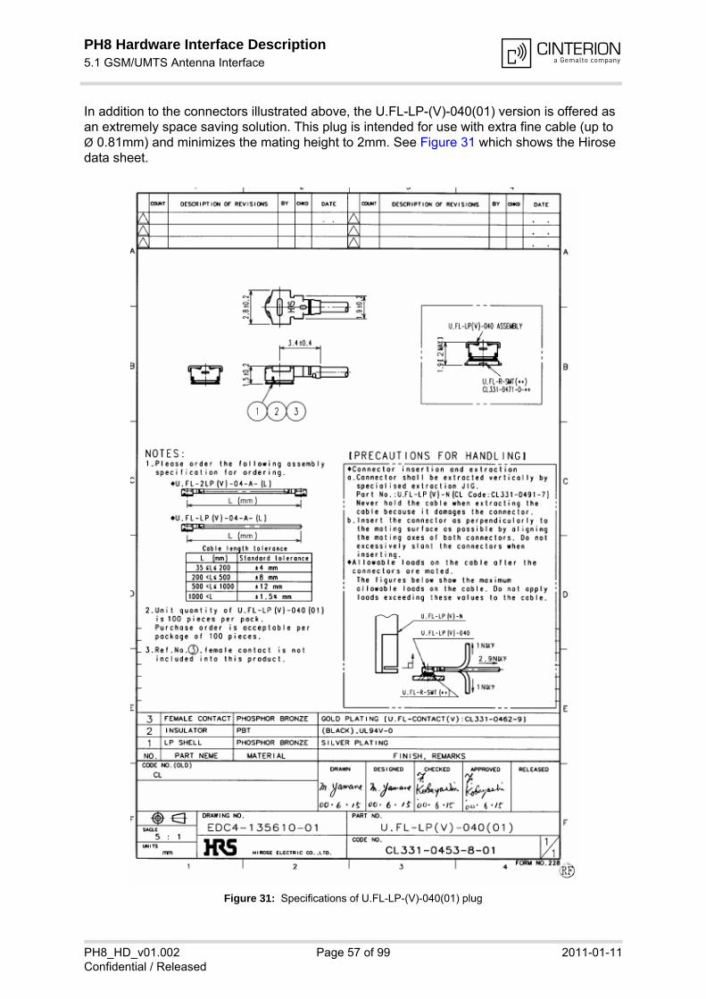
PH8 Hardware Interface Description5.1 GSM/UMTS Antenna Interface59
PH8_HD_v01.002 Page 57 of 99 2011-01-11Confidential / Released
In addition to the connectors illustrated above, the U.FL-LP-(V)-040(01) version is offered as an extremely space saving solution. This plug is intended for use with extra fine cable (up to Ø 0.81mm) and minimizes the mating height to 2mm. See Figure 31 which shows the Hirose data sheet.
Figure 31: Specifications of U.FL-LP-(V)-040(01) plug

PH8 Hardware Interface Description5.1 GSM/UMTS Antenna Interface59
PH8_HD_v01.002 Page 58 of 99 2011-01-11Confidential / Released
Table 18: Ordering information for Hirose U.FL Series
Item Part number HRS number
Connector on PH8 U.FL-R-SMT CL331-0471-0-10
Right-angle plug shell for Ø 0.81mm cable
U.FL-LP-040 CL331-0451-2
Right-angle plug for Ø 0.81mm cable
U.FL-LP(V)-040 (01) CL331-053-8-01
Right-angle plug for Ø 1.13mm cable
U.FL-LP-068 CL331-0452-5
Right-angle plug for Ø 1.32mm cable
U.FL-LP-066 CL331-0452-5
Extraction jig E.FL-LP-N CL331-04441-9

PH8 Hardware Interface Description5.2 GPS Antenna Interface59
PH8_HD_v01.002 Page 59 of 99 2011-01-11Confidential / Released
5.2 GPS Antenna Interface
In addition to the RF antenna interface PH8 also has a GPS antenna interface. See Section 7.1 to find out where the GPS antenna connector is located. The GPS antenna installation and con-nector are the same as for the RF antenna interface (see Section 5.1.1 and Section 5.1.2).
It is possible to connect active or passive GPS antennas. In either case they must have 50 Ohm impedance. The simultaneous operation of GSM and GPS has been implemented. For electri-cal characteristics see Section 6.9.
Active 3V GPS antennas can be supplied via the GPS antenna interface, if the supply voltage is switched on. This is done by AT command AT^SGPSS (for details see [1]). The available current is limited to prevent short circuits.
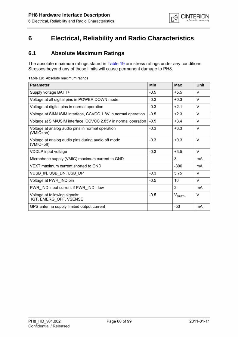
PH8 Hardware Interface Description6 Electrical, Reliability and Radio Characteristics81
PH8_HD_v01.002 Page 60 of 99 2011-01-11Confidential / Released
6 Electrical, Reliability and Radio Characteristics
6.1 Absolute Maximum Ratings
The absolute maximum ratings stated in Table 19 are stress ratings under any conditions. Stresses beyond any of these limits will cause permanent damage to PH8.
Table 19: Absolute maximum ratings
Parameter Min Max Unit
Supply voltage BATT+ -0.5 +5.5 V
Voltage at all digital pins in POWER DOWN mode -0.3 +0.3 V
Voltage at digital pins in normal operation -0.3 +2.1 V
Voltage at SIM/USIM interface, CCVCC 1.8V in normal operation -0.5 +2.3 V
Voltage at SIM/USIM interface, CCVCC 2.85V in normal operation -0.5 +3.4 V
Voltage at analog audio pins in normal operation(VMIC=on)
-0.3 +3.3 V
Voltage at analog audio pins during audio off mode(VMIC=off)
-0.3 +0.3 V
VDDLP input voltage -0.3 +3.5 V
Microphone supply (VMIC) maximum current to GND 3 mA
VEXT maximum current shorted to GND -300 mA
VUSB_IN, USB_DN, USB_DP -0.3 5.75 V
Voltage at PWR_IND pin -0.5 10 V
PWR_IND input current if PWR_IND= low 2 mA
Voltage at following signals: IGT, EMERG_OFF, VSENSE
-0.5 VBATT+ V
GPS antenna supply limited output current -53 mA

PH8 Hardware Interface Description6.2 Operating Temperatures81
PH8_HD_v01.002 Page 61 of 99 2011-01-11Confidential / Released
6.2 Operating Temperatures
The maximum allowable ambient temperature that causes the module to shut down dependson various conditions. The following Table 21 and Table 22 show sample lab environment con-ditions with GPS switched on (NMEA data output) and USB connected. Please be aware thatthe maximum ambient temperature may vary for your application.
Table 20: Board temperature
Parameter Min Typ Max Unit
Operating temperature range -30 +25 +85 °C
Restricted temperature range -40 +95 °C
Automatic shutdown1
Temperature measured on PH8 board
1. Due to temperature measurement uncertainty, a tolerance on the stated shutdown thresholds may occur. The possible deviation is in the range of ± 2°C at the overtemperature and undertemperature limit.
<-40 --- >+95 °C
Table 21: Sample operating conditions without forced air circulation (according to IEC 60068-2)1
1. The thermal resistance of the module (board-to-ambient) was measured to be about Rth=20K/W
Mode Ambient Temperature
Voltage RF Power OperatingDuration
GSM, GPRS/EDGE Class 8
+75°C VBATT+ < 4.2V Max.
GPRS/EDGE Class 10ROPR=4 +65°C VBATT+ < 3.8V Max.
GPRS/EDGE Class 12ROPR=4ROPR=8
+55°C+65°C
VBATT+ < 3.8VVBATT+ < 3.8V
Max.Reduced
GPRS/EDGE Class 12ROPR=4 +65°C VBATT+ < 3.8V Max. < 2min
WCDMA +55°C VBATT+ < 3.8V Max. WCDMA +65°C VBATT+ < 3.8V < 10dBm WCDMA +70°C VBATT+ < 3.8V < 0dBm WCDMA +65°C VBATT+ < 3.8V Max. < 3min
Table 22: Sample operating conditions with forced air circulation (air speed 0.9m/s)
Mode Ambient Temperature
Voltage RF Power OperatingDuration
GSM, GPRS/EDGE Class 8
+80°C VBATT+ < 4.2V Max.
GPRS/EDGE Class 10ROPR=4 +75°C VBATT+ < 3.8V Max.
GPRS/EDGE Class 12ROPR=4ROPR=8
+65°C+75°C
VBATT+ < 3.8VVBATT+ < 3.8V
Max.Reduced
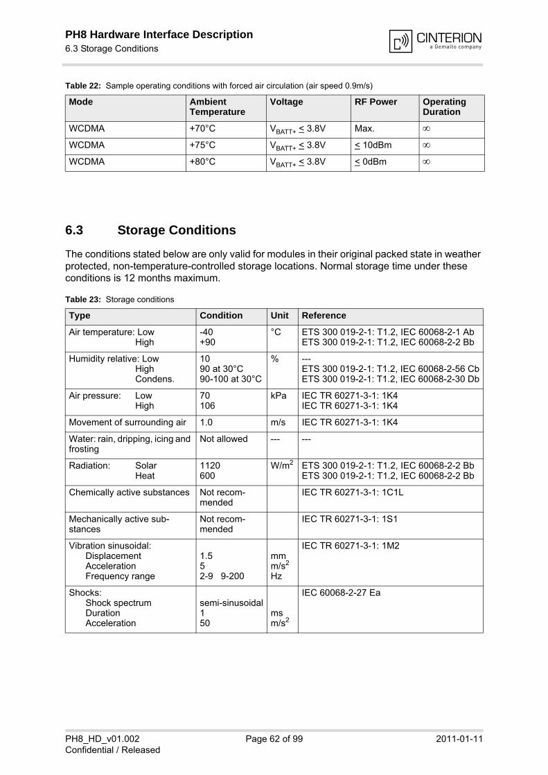
PH8 Hardware Interface Description6.3 Storage Conditions81
PH8_HD_v01.002 Page 62 of 99 2011-01-11Confidential / Released
6.3 Storage Conditions
The conditions stated below are only valid for modules in their original packed state in weather protected, non-temperature-controlled storage locations. Normal storage time under these conditions is 12 months maximum.
WCDMA +70°C VBATT+ < 3.8V Max. WCDMA +75°C VBATT+ < 3.8V < 10dBm WCDMA +80°C VBATT+ < 3.8V < 0dBm
Table 23: Storage conditions
Type Condition Unit Reference
Air temperature: LowHigh
-40+90
°C ETS 300 019-2-1: T1.2, IEC 60068-2-1 AbETS 300 019-2-1: T1.2, IEC 60068-2-2 Bb
Humidity relative: LowHighCondens.
1090 at 30°C90-100 at 30°C
% ---ETS 300 019-2-1: T1.2, IEC 60068-2-56 CbETS 300 019-2-1: T1.2, IEC 60068-2-30 Db
Air pressure: LowHigh
70106
kPa IEC TR 60271-3-1: 1K4IEC TR 60271-3-1: 1K4
Movement of surrounding air 1.0 m/s IEC TR 60271-3-1: 1K4
Water: rain, dripping, icing and frosting
Not allowed --- ---
Radiation: SolarHeat
1120600
W/m2 ETS 300 019-2-1: T1.2, IEC 60068-2-2 BbETS 300 019-2-1: T1.2, IEC 60068-2-2 Bb
Chemically active substances Not recom-mended
IEC TR 60271-3-1: 1C1L
Mechanically active sub-stances
Not recom-mended
IEC TR 60271-3-1: 1S1
Vibration sinusoidal:DisplacementAccelerationFrequency range
1.552-9 9-200
mmm/s2
Hz
IEC TR 60271-3-1: 1M2
Shocks:Shock spectrumDurationAcceleration
semi-sinusoidal150
msm/s2
IEC 60068-2-27 Ea
Table 22: Sample operating conditions with forced air circulation (air speed 0.9m/s)
Mode Ambient Temperature
Voltage RF Power OperatingDuration
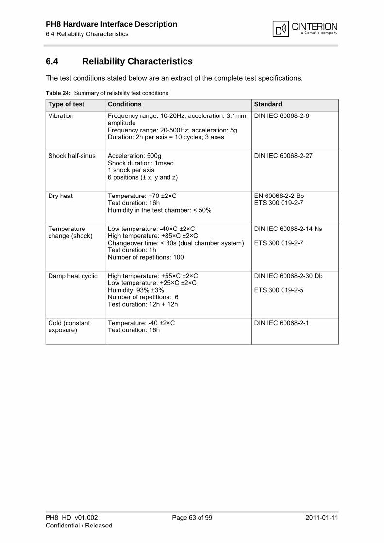
PH8 Hardware Interface Description6.4 Reliability Characteristics81
PH8_HD_v01.002 Page 63 of 99 2011-01-11Confidential / Released
6.4 Reliability Characteristics
The test conditions stated below are an extract of the complete test specifications.
Table 24: Summary of reliability test conditions
Type of test Conditions Standard
Vibration Frequency range: 10-20Hz; acceleration: 3.1mm amplitudeFrequency range: 20-500Hz; acceleration: 5gDuration: 2h per axis = 10 cycles; 3 axes
DIN IEC 60068-2-6
Shock half-sinus Acceleration: 500gShock duration: 1msec1 shock per axis6 positions (± x, y and z)
DIN IEC 60068-2-27
Dry heat Temperature: +70 ±2×CTest duration: 16hHumidity in the test chamber: < 50%
EN 60068-2-2 Bb ETS 300 019-2-7
Temperature change (shock)
Low temperature: -40×C ±2×CHigh temperature: +85×C ±2×CChangeover time: < 30s (dual chamber system)Test duration: 1hNumber of repetitions: 100
DIN IEC 60068-2-14 Na
ETS 300 019-2-7
Damp heat cyclic High temperature: +55×C ±2×CLow temperature: +25×C ±2×CHumidity: 93% ±3%Number of repetitions: 6Test duration: 12h + 12h
DIN IEC 60068-2-30 Db
ETS 300 019-2-5
Cold (constant exposure)
Temperature: -40 ±2×CTest duration: 16h
DIN IEC 60068-2-1
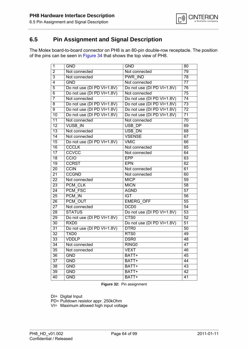
PH8 Hardware Interface Description6.5 Pin Assignment and Signal Description81
PH8_HD_v01.002 Page 64 of 99 2011-01-11Confidential / Released
6.5 Pin Assignment and Signal Description
The Molex board-to-board connector on PH8 is an 80-pin double-row receptacle. The position of the pins can be seen in Figure 34 that shows the top view of PH8.
Figure 32: Pin assignment
DI= Digital InputPD= Pulldown resistor appr. 250kOhmVI= Maximum allowed high input voltage
1 GND GND 802 Not connected Not connected 793 Not connected PWR_IND 784 GND Not connected 775 Do not use (DI PD VI=1.8V) Do not use (DI PD VI=1.8V) 766 Do not use (DI PD VI=1.8V) Not connected 757 Not connected Do not use (DI PD VI=1.8V) 748 Do not use (DI PD VI=1.8V) Do not use (DI PD VI=1.8V) 739 Do not use (DI PD VI=1.8V) Do not use (DI PD VI=1.8V) 7210 Do not use (DI PD VI=1.8V) Do not use (DI PD VI=1.8V) 7111 Not connected Not connected 7012 VUSB_IN USB_DP 6913 Not connected USB_DN 6814 Not connected VSENSE 6715 Do not use (DI PD VI=1.8V) VMIC 6616 CCCLK Not connected 6517 CCVCC Not connected 6418 CCIO EPP 6319 CCRST EPN 6220 CCIN Not connected 6121 CCGND Not connected 6022 Not connected MICP 5923 PCM_CLK MICN 5824 PCM_FSC AGND 5725 PCM_IN IGT 5626 PCM_OUT EMERG_OFF 5527 Not connected DCD0 5428 STATUS Do not use (DI PD VI=1.8V) 5329 Do not use (DI PD VI=1.8V) CTS0 5230 RXD0 Do not use (DI PD VI=1.8V) 5131 Do not use (DI PD VI=1.8V) DTR0 5032 TXD0 RTS0 4933 VDDLP DSR0 4834 Not connected RING0 4735 Not connected VEXT 4636 GND BATT+ 4537 GND BATT+ 4438 GND BATT+ 4339 GND BATT+ 4240 GND BATT+ 41

PH8 Hardware Interface Description6.5 Pin Assignment and Signal Description81
PH8_HD_v01.002 Page 65 of 99 2011-01-11Confidential / Released
Please note that the reference voltages listed in Table 25 are the values measured directly on the PH8 module. They do not apply to the accessories connected.
Table 25: Signal description
Function Signal name IO Signal form and level Comment
Power supply
BATT+ I VImax = 4.2VVInorm = 3.8VVImin = 3.3V during Tx burst on board
I 2A, during Tx burst (GSM)
Pins of BATT+ and GND must be connected in par-allel for supply purposes because higher peak cur-rents may occur.
Minimum voltage must not fall below 3.3V including drop, ripple, spikes.
n Tx = n x 577µs peak current every 4.615ms
Power supply
GND Ground Application Ground
BATT+ sense line
VSENSE I VImax= BATT+ + 400mVVImin= 0.6V
Connecting VSENSE directly to the BATT+ source.
External supply voltage
VEXT O Normal Operation:VOnorm = 1.80V +1% -5%IOmax = -50mA
CLmax = 1µF
IOmax is reduced to 10mA, if power save mode for VEXT is enabled (see Comment).
VEXT may be used for application circuits.
If unused keep pin open and enable power save mode via AT^SCFG= "MEopMode/PowerMgmt/VExt", "low" (see [1])
Not available in Power down mode.
The external digital logic must not cause any spikes or glitches on voltage VEXT.
Ignition IGT I RPU 160k, CI 1nFVOHmax=1.85VVIHmax =2.2V VIHmin = 1.17VVILmax = 300mV
Low impulse width > 100ms
This signal switches the module ON.
It is recommended to drive this line low by an open drain or open collector driver connected to GND.
Emer-gency Off
EMERG_OFF I RPU 160k, CI 1nFVOHmax=1.85VVIHmax =2.2V VIHmin = 1.17VVILmax = 300mV
~~|___|~~ low impulse width > 40ms
It is recommended to drive this line low by an open drain or open collector driver connected to GND.
If unused keep pin open.
RTC Back up
VDDLP O VOmax = 3.20V while BATT+ =>3.3VRI = 1.8k
If unused keep pin open.
I VI = 1.5V…3.25V at Imax= 10µA while BATT+ = 0V

PH8 Hardware Interface Description6.5 Pin Assignment and Signal Description81
PH8_HD_v01.002 Page 66 of 99 2011-01-11Confidential / Released
Connectiv-ity Status
STATUS O VOLmax = 0.45V at I = 2mAVOHmin = 1.35V at I = -2mAVOHmax = 1.85V
Status signalling e.g. with ext. LED circuit
SIM Card detection
CCIN I RPU 110kVOHmax=1.9VVIHmin = 1.15V VIHmax= 1.9VVILmax = 0.6V
CCIN = Low, SIM card inserted.
CCIN is protected against ESD with a special diode array.
If unused connect to GND.
3V SIM Card Inter-face
CCRST O VOLmax = 0.45V at I = 1mAVOHmin = 2.40V at I = -1mAVOHmax = 2.9V
Maximum cable length or copper track should be not longer than 100mm to SIM card holder.
The signals CCRST, CCIO, CCCLK and CCVCC are protected against ESD with a special diode array.
CCIO I/O RPU 4.7kVILmax = 1VVILmin = -0.3VVIHmin = 1.85VVIHmax = 3.2V
VOLmax = 0.45V at I = 1mAVOHmin = 2.3V at I = -0.1mAVOHmax = 2.9V
CCCLK O VOLmax = 0.45V at I = 1mAVOHmin = 2.40V at I = -1mAVOHmax = 2.9V
CCVCC O VOmin = 2.8V VOtyp =2.85VVOmax = 2.9VIOmax = -50mA
CCGND Ground
1.8V SIM Card Inter-face
CCRST O VOLmax = 0.45V at I = 1mAVOHmin = 1.35V at I = -1mAVOHmax = 1.85V
CCIO I/O RI 4.7kVILmax = 0.65VVILmin = -0.3VVIHmin = 1.20VVIHmax = 1.85V
VOLmax = 0.45V at I = 1mAVOHmin = 1.25V at I = -0.1mAVOHmax = 1.85V
CCCLK O VOLmax = 0.45V at I = 1mAVOHmin = 1.35V at I = -1mAVOHmax = 1.85V
CCVCC O VOmin = 1.75V VOtyp = 1.80VVOmax = 1.85VIOmax = -50mA
CCGND Ground
Table 25: Signal description
Function Signal name IO Signal form and level Comment
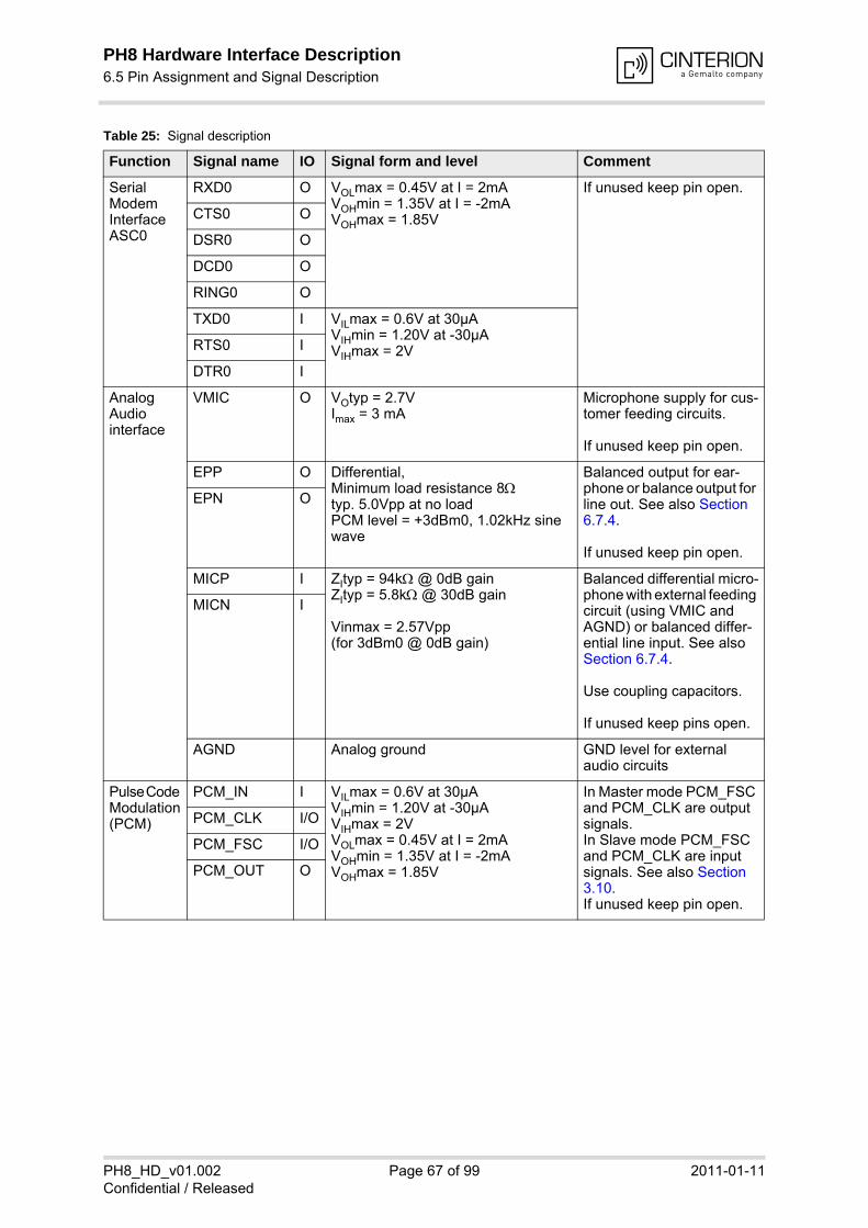
PH8 Hardware Interface Description6.5 Pin Assignment and Signal Description81
PH8_HD_v01.002 Page 67 of 99 2011-01-11Confidential / Released
Serial Modem Interface ASC0
RXD0 O VOLmax = 0.45V at I = 2mAVOHmin = 1.35V at I = -2mAVOHmax = 1.85V
If unused keep pin open.
CTS0 O
DSR0 O
DCD0 O
RING0 O
TXD0 I VILmax = 0.6V at 30µAVIHmin = 1.20V at -30µAVIHmax = 2VRTS0 I
DTR0 I
Analog Audio interface
VMIC O VOtyp = 2.7V Imax = 3 mA
Microphone supply for cus-tomer feeding circuits.
If unused keep pin open.
EPP O Differential, Minimum load resistance 8typ. 5.0Vpp at no loadPCM level = +3dBm0, 1.02kHz sine wave
Balanced output for ear-phone or balance output for line out. See also Section 6.7.4.
If unused keep pin open.
EPN O
MICP I ZItyp = 94k @ 0dB gainZItyp = 5.8k @ 30dB gain
Vinmax = 2.57Vpp (for 3dBm0 @ 0dB gain)
Balanced differential micro-phone with external feeding circuit (using VMIC and AGND) or balanced differ-ential line input. See also Section 6.7.4.
Use coupling capacitors.
If unused keep pins open.
MICN I
AGND Analog ground GND level for external audio circuits
Pulse Code Modulation(PCM)
PCM_IN I VILmax = 0.6V at 30µAVIHmin = 1.20V at -30µAVIHmax = 2VVOLmax = 0.45V at I = 2mAVOHmin = 1.35V at I = -2mAVOHmax = 1.85V
In Master mode PCM_FSC and PCM_CLK are output signals. In Slave mode PCM_FSC and PCM_CLK are input signals. See also Section 3.10.If unused keep pin open.
PCM_CLK I/O
PCM_FSC I/O
PCM_OUT O
Table 25: Signal description
Function Signal name IO Signal form and level Comment

PH8 Hardware Interface Description6.5 Pin Assignment and Signal Description81
PH8_HD_v01.002 Page 68 of 99 2011-01-11Confidential / Released
Power Indicator
PWR_IND O VIHmax = 10VVOLmax = 0.4V at Imax = 2mA
PWR_IND (Power Indica-tor) notifies the module’s on/off state.
PWR_IND is an open col-lector that needs to be con-nected to an external pull-up resistor. Low state of the open collector indicates that the module is on. Vice versa, high level notifies the power-down mode.
Therefore, the pin may be used to enable external voltage regulators which supply an external logic for communication with the module, e.g. level convert-ers.
USB VUSB_IN I VINmin = 3.0VVINmax = 5.25VActive current IItyp = 15µA (max 50µA)Suspend currentIItyp =15µA (max 110µA)
For this line an external pull down resistor (10k…40k) is recommended (see Section 3.6).
If the USB interface is not used please connect this line to GND.
USB_DN I/O All electrical characteristics according to USB Implementers’ Forum, USB 2.0 Full or High Speed Specification.
If lines are unused keep pins open.
USB_DP I/O
Table 25: Signal description
Function Signal name IO Signal form and level Comment

PH8 Hardware Interface Description6.6 Power Supply Ratings81
PH8_HD_v01.002 Page 69 of 99 2011-01-11Confidential / Released
6.6 Power Supply Ratings
Table 26: Power supply ratings
Description Conditions Min Typ Max Unit
BATT+ Supply voltage Directly measured at Module.Voltage must stay within the min/max values, including voltage drop, ripple, spikes
3.3 3.8 4.2 V
Maximum allowed voltage drop dur-ing transmit burst
Normal condition, power control level for Pout max
400 mV
Voltage ripple Normal condition, power control level for Pout max@ f <= 250 kHz@ f > 250 kHz
20 16
mVSSmVSS
IVDDLP @ 3V
OFF State supply current
RTC backup @ BATT+ = 0V 4.0 µA
IBATT+ 1 OFF State supply
current POWER DOWN 39 µA
Average GSM / GPRS supply cur-rent (GPS off)
SLEEP2 (USB Suspend or USB discon-nected and no communication via ASC0) @ DRX=9
1.8 mA
SLEEP2 (USB Suspend or USB discon-nected and no communication via ASC0) @ DRX=5
2.4 mA
SLEEP2 (USB Suspend or USB discon-nected and no communication via ASC0) @ DRX=2
3.6 mA
IDLE3 (SLEEP disabled, USB disconnected, UART active) @ DRX=2
38 mA
IDLE3 (SLEEP disabled, USB active) @ DRX=2
56 mA
Voice Call GSM850/900; PCL=5 290 mA
GPRS Data transfer GSM850/900; PCL=5; 1Tx/4Rx
ROPR=8 (max. reduction)
285 mA
ROPR=4 (no reduction)
285 mA
GPRS Data transfer GSM850/900; PCL=5; 2Tx/3Rx
ROPR=8 (max. reduction)
375 mA
ROPR=4 (no reduction)
510 mA
GPRS Data transfer GSM850/900; PCL=5; 4Tx/1Rx
ROPR=8 (max. reduction)
490 mA
ROPR=4 (no reduction)
860 mA

PH8 Hardware Interface Description6.6 Power Supply Ratings81
PH8_HD_v01.002 Page 70 of 99 2011-01-11Confidential / Released
IBATT+ 1 Average GSM /
GPRS supply current (GPS off)
EDGE Data transfer GSM850/900; PCL=5; 1Tx/4Rx
ROPR=8 (max. reduction)
180 mA
ROPR=4 (no reduction)
180 mA
EDGE Data transfer GSM850/900; PCL=5; 2Tx/3Rx
ROPR=8 (max. reduction)
240 mA
ROPR=4 (no reduction)
290 mA
EDGE Data transfer GSM850/900; PCL=5; 4Tx/1Rx
ROPR=8 (max. reduction)
275 mA
ROPR=4 (no reduction)
470 mA
Voice Call GSM1800/1900; PCL=0 205 mA
GPRS Data transfer GSM1800/1900; PCL=0; 1Tx/4Rx
ROPR=8 (max. reduction)
190 mA
ROPR=4 (no reduction)
190 mA
GPRS Data transfer GSM1800/1900; PCL=0; 2Tx/3Rx
ROPR=8 (max. reduction)
245 mA
ROPR=4 (no reduction)
305 mA
GPRS Data transfer GSM1800/1900; PCL=0; 4Tx/1Rx
ROPR=8 (max. reduction)
320 mA
ROPR=4 (no reduction)
505 mA
EDGE Data transfer GSM1800/1900; PCL=0; 1Tx/4Rx
ROPR=8 (max. reduction)
150 mA
ROPR=4 (no reduction)
150 mA
EDGE Data transfer GSM1800/1900; PCL=0; 2Tx/3Rx
ROPR=8 (max. reduction)
200 mA
ROPR=4 (no reduction)
230 mA
EDGE Data transfer GSM1800/1900; PCL=0; 4Tx/1Rx
ROPR=8 (max. reduction)
260 mA
ROPR=4 (no reduction)
360 mA
Peak current dur-ing GSM transmit burst
VOICE Call GSM850/900; PCL=5 1.95 2.74 A
VOICE Call GSM1800/1900; PCL=0 1.1 2.14 A
Average GSM / GPS supply cur-rent (GPS on)
GSM active (UART/USB active); @DRX=2 & GPS NMEA output on5
75 mA
Table 26: Power supply ratings
Description Conditions Min Typ Max Unit
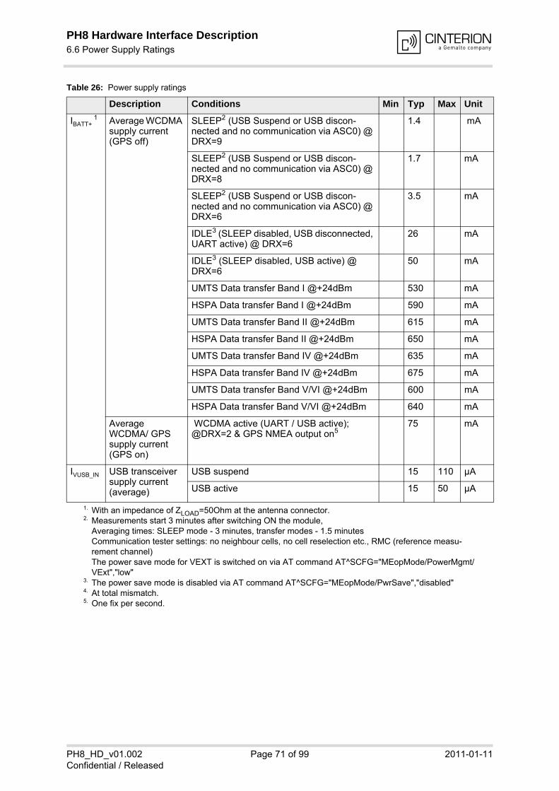
PH8 Hardware Interface Description6.6 Power Supply Ratings81
PH8_HD_v01.002 Page 71 of 99 2011-01-11Confidential / Released
IBATT+ 1 Average WCDMA
supply current (GPS off)
SLEEP2 (USB Suspend or USB discon-nected and no communication via ASC0) @ DRX=9
1.4 mA
SLEEP2 (USB Suspend or USB discon-nected and no communication via ASC0) @ DRX=8
1.7 mA
SLEEP2 (USB Suspend or USB discon-nected and no communication via ASC0) @ DRX=6
3.5 mA
IDLE3 (SLEEP disabled, USB disconnected, UART active) @ DRX=6
26 mA
IDLE3 (SLEEP disabled, USB active) @ DRX=6
50 mA
UMTS Data transfer Band I @+24dBm 530 mA
HSPA Data transfer Band I @+24dBm 590 mA
UMTS Data transfer Band II @+24dBm 615 mA
HSPA Data transfer Band II @+24dBm 650 mA
UMTS Data transfer Band IV @+24dBm 635 mA
HSPA Data transfer Band IV @+24dBm 675 mA
UMTS Data transfer Band V/VI @+24dBm 600 mA
HSPA Data transfer Band V/VI @+24dBm 640 mA
Average WCDMA/ GPS supply current (GPS on)
WCDMA active (UART / USB active); @DRX=2 & GPS NMEA output on5
75 mA
IVUSB_IN USB transceiver supply current (average)
USB suspend 15 110 µA
USB active 15 50 µA
1. With an impedance of ZLOAD=50Ohm at the antenna connector.2. Measurements start 3 minutes after switching ON the module,
Averaging times: SLEEP mode - 3 minutes, transfer modes - 1.5 minutesCommunication tester settings: no neighbour cells, no cell reselection etc., RMC (reference measu-rement channel)The power save mode for VEXT is switched on via AT command AT^SCFG="MEopMode/PowerMgmt/VExt","low"
3. The power save mode is disabled via AT command AT^SCFG="MEopMode/PwrSave","disabled"4. At total mismatch.5. One fix per second.
Table 26: Power supply ratings
Description Conditions Min Typ Max Unit

PH8 Hardware Interface Description6.7 Electrical Characteristics of the Voiceband Part81
PH8_HD_v01.002 Page 72 of 99 2011-01-11Confidential / Released
6.7 Electrical Characteristics of the Voiceband Part
6.7.1 Setting Audio Parameters by AT Commands
Audio mode 1 is the basic audio mode optimized for the Votronic reference handset (see Sec-tion 10.1). The default parameters are determined for type approval and are not adjustable with AT commands.
The audio modes 2 to 6 can be temporarily adjusted according to the AT command parameters listed in the table below. The audio parameters are set with the AT commands AT^SNFI as well as AT^SNFO and stored volatile for the current audio mode (see [1]). For a model of how the parameters influence the audio signal path see Section 6.7.2.
Table 27: Audio parameters adjustable by AT command
Parameter Influence to Range Gain range Calculation
AT^SNFI=
micAmp1 MICP/MICN second analog ampli-fier gain of before ADC
0,1 0 or 20dB
micAmp2 MICP/MICN first analog amplifier gain of before ADC
0…63 -12…35.25dB 0.75dB steps
micTxVol Digital gain of input signal after ADC 0,1...65535
Mute,-84...+12dB 20 * log (micTxVol/
16384)
AT^SNFO=
cdcRxGain Analog gain of output signal after summation of sidetone
0...63 -57...+6dB 1dB steps
rxVol Digital Volume of output signal after speech decoder, before summation of sidetone and DAC
0,1…41
Mute,-48...+12dB 1.5dB steps
stGain Digital attenuation of sidetone 0,1...65535
Mute,-96...0dB 20 * log (stGain/
16384) -12

PH8 Hardware Interface Description6.7 Electrical Characteristics of the Voiceband Part81
PH8_HD_v01.002 Page 73 of 99 2011-01-11Confidential / Released
6.7.2 Audio Programming Model
The audio programming model shows how the signal path can be influenced by varying AT command parameters: AT^SNFI allows to set the parameters <micAmp1>, <micAmp2> and <micTxVol>, whereas the parameters <cdcRxGain>, <stGain> and <rxVol> can be adjusted with AT^SNFO. For more information on the AT commands and parameters see Section 6.7.1 and [1].
Figure 33: Audio programming model
6.7.3 Characteristics of Audio Modes
The electrical characteristics of the voiceband part depend on the current audio mode set with AT command. All values are noted for default gains, e.g. the default parameters are left unchanged.
Table 28: Voiceband characteristics
Audio mode no.AT^SNFS=
1 2 3 4 5 6
Name Default Handset
Router User Handset
Headset Speaker phone
Transpar-ent
Purpose DSB with Votronic handset
Analog phone interface
Mono Head-set
Handheld speaker-phone
Direct access to speech coder
TX-Filters Adjusted Flat Adjusted Flat Flat Flat
Microphonefeeding
AD
Speechcoder
<stGain>
MIC
AD Speech
decoderEP8 Ohms
PH8VMIC
<micTxVol>
<cdcRxGain>
AT parameters are given in brackets <...> and marked red and italic.
<micAmp2><micAmp1>
<rxVol><io>
PCM4PCM
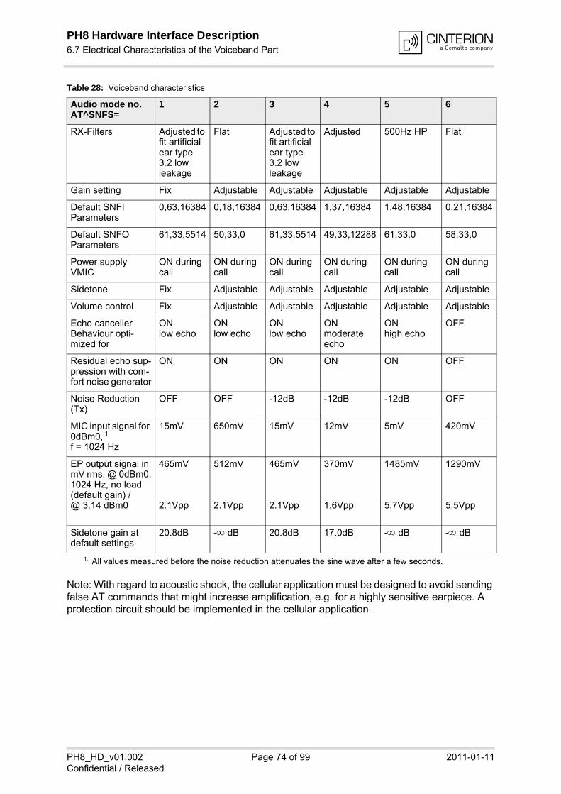
PH8 Hardware Interface Description6.7 Electrical Characteristics of the Voiceband Part81
PH8_HD_v01.002 Page 74 of 99 2011-01-11Confidential / Released
Note: With regard to acoustic shock, the cellular application must be designed to avoid sending false AT commands that might increase amplification, e.g. for a highly sensitive earpiece. A protection circuit should be implemented in the cellular application.
RX-Filters Adjusted to fit artificial ear type 3.2 low leakage
Flat Adjusted to fit artificial ear type 3.2 low leakage
Adjusted 500Hz HP Flat
Gain setting Fix Adjustable Adjustable Adjustable Adjustable Adjustable
Default SNFI Parameters
0,63,16384 0,18,16384 0,63,16384 1,37,16384 1,48,16384 0,21,16384
Default SNFO Parameters
61,33,5514 50,33,0 61,33,5514 49,33,12288 61,33,0 58,33,0
Power supply VMIC
ON during call
ON during call
ON during call
ON during call
ON during call
ON during call
Sidetone Fix Adjustable Adjustable Adjustable Adjustable Adjustable
Volume control Fix Adjustable Adjustable Adjustable Adjustable Adjustable
Echo cancellerBehaviour opti-mized for
ONlow echo
ONlow echo
ONlow echo
ONmoderate echo
ONhigh echo
OFF
Residual echo sup-pression with com-fort noise generator
ON ON ON ON ON OFF
Noise Reduction (Tx)
OFF OFF -12dB -12dB -12dB OFF
MIC input signal for 0dBm0, 1
f = 1024 Hz
15mV 650mV 15mV 12mV 5mV 420mV
EP output signal in mV rms. @ 0dBm0,1024 Hz, no load (default gain) /@ 3.14 dBm0
465mV
2.1Vpp
512mV
2.1Vpp
465mV
2.1Vpp
370mV
1.6Vpp
1485mV
5.7Vpp
1290mV
5.5Vpp
Sidetone gain at default settings
20.8dB - dB 20.8dB 17.0dB - dB - dB
1. All values measured before the noise reduction attenuates the sine wave after a few seconds.
Table 28: Voiceband characteristics
Audio mode no.AT^SNFS=
1 2 3 4 5 6

PH8 Hardware Interface Description6.7 Electrical Characteristics of the Voiceband Part81
PH8_HD_v01.002 Page 75 of 99 2011-01-11Confidential / Released
6.7.4 Voiceband Receive Path
Test conditions:• The values specified below were tested to 1024Hz using AT^SNFO=57,33,0 in audio mode
6 during a GSM FR voice call unless otherwise stated.
6.7.5 Voiceband Transmit Path
Test conditions:• The values specified below were tested to 1024Hz using AT^SNFI=0,16,16384 in audio
mode 6 during a GSM FR voice call unless otherwise stated.
Table 29: Voiceband receive path
Parameter Min Typ Max Unit Test condition / remark
Maximum differential output voltage (peak to peak)EPP to EPN
4.05.0
VV
8, No load,@ 3.14 dBm0 (Full Scale)
Nominal differential output voltage (peak to peak)EPP to EPN
2.83.4
VV
8, No load,@ 0 dBm0 (Nominal level)
Output bias voltage 1.5 V From EPP or EPN to GND
Differential output load resistance 8
Table 30: Voiceband transmit path
Parameter Min Typ Max Unit Test condition / Remark
Full scale input voltage (peak to peak) for 3.14dBm0MICP to MICN
2.57 V Balanced
Nominal input voltage (rms) for 0dBm0MICP to MICN
0.64 V Balanced
Input amplifier 1 gain (micAmp1) 0 20 dB Set with AT^SNFI
Input amplifier 2 gain in 1.5dB steps (micAmp2)
-12 35.25 dB Set with AT^SNFI
Fine scaling by DSP (micTxVol) -84 12 dB Set with AT^SNFI
Microphone supply voltage VMIC 2.7 V No load
Microphone supply voltage VMIC 2.6 V @ 3mA
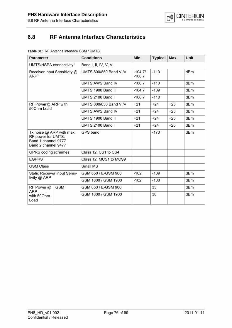
PH8 Hardware Interface Description6.8 RF Antenna Interface Characteristics81
PH8_HD_v01.002 Page 76 of 99 2011-01-11Confidential / Released
6.8 RF Antenna Interface Characteristics
Table 31: RF Antenna interface GSM / UMTS
Parameter Conditions Min. Typical Max. Unit
UMTS/HSPA connectivity1 Band I, II, IV, V, VI
Receiver Input Sensitivity @ ARP1
UMTS 800/850 Band VI/V -104.7/ -106.7
-110 dBm
UMTS AWS Band IV -106.7 -110 dBm
UMTS 1900 Band II -104.7 -109 dBm
UMTS 2100 Band I -106.7 -110 dBm
RF Power@ ARP with 50Ohm Load
UMTS 800/850 Band VI/V +21 +24 +25 dBm
UMTS AWS Band IV +21 +24 +25 dBm
UMTS 1900 Band II +21 +24 +25 dBm
UMTS 2100 Band I +21 +24 +25 dBm
Tx noise @ ARP with max. RF power for UMTS:Band 1 channel 9777Band 2 channel 9477
GPS band -170 dBm
GPRS coding schemes Class 12, CS1 to CS4
EGPRS Class 12, MCS1 to MCS9
GSM Class Small MS
Static Receiver input Sensi-tivity @ ARP
GSM 850 / E-GSM 900 -102 -109 dBm
GSM 1800 / GSM 1900 -102 -108 dBm
RF Power @ ARP with 50Ohm Load
GSM GSM 850 / E-GSM 900 33 dBm
GSM 1800 / GSM 1900 30 dBm
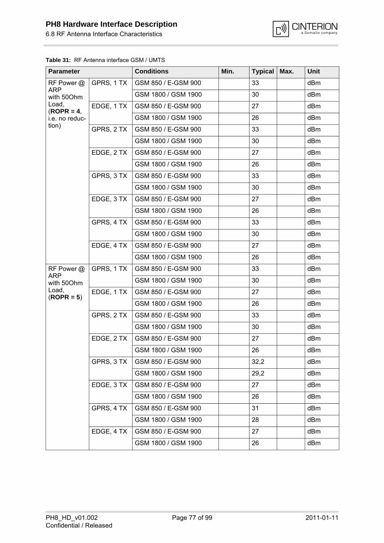
PH8 Hardware Interface Description6.8 RF Antenna Interface Characteristics81
PH8_HD_v01.002 Page 77 of 99 2011-01-11Confidential / Released
RF Power @ ARP with 50Ohm Load, (ROPR = 4, i.e. no reduc-tion)
GPRS, 1 TX GSM 850 / E-GSM 900 33 dBm
GSM 1800 / GSM 1900 30 dBm
EDGE, 1 TX GSM 850 / E-GSM 900 27 dBm
GSM 1800 / GSM 1900 26 dBm
GPRS, 2 TX GSM 850 / E-GSM 900 33 dBm
GSM 1800 / GSM 1900 30 dBm
EDGE, 2 TX GSM 850 / E-GSM 900 27 dBm
GSM 1800 / GSM 1900 26 dBm
GPRS, 3 TX GSM 850 / E-GSM 900 33 dBm
GSM 1800 / GSM 1900 30 dBm
EDGE, 3 TX GSM 850 / E-GSM 900 27 dBm
GSM 1800 / GSM 1900 26 dBm
GPRS, 4 TX GSM 850 / E-GSM 900 33 dBm
GSM 1800 / GSM 1900 30 dBm
EDGE, 4 TX GSM 850 / E-GSM 900 27 dBm
GSM 1800 / GSM 1900 26 dBm
RF Power @ ARPwith 50Ohm Load,(ROPR = 5)
GPRS, 1 TX GSM 850 / E-GSM 900 33 dBm
GSM 1800 / GSM 1900 30 dBm
EDGE, 1 TX GSM 850 / E-GSM 900 27 dBm
GSM 1800 / GSM 1900 26 dBm
GPRS, 2 TX GSM 850 / E-GSM 900 33 dBm
GSM 1800 / GSM 1900 30 dBm
EDGE, 2 TX GSM 850 / E-GSM 900 27 dBm
GSM 1800 / GSM 1900 26 dBm
GPRS, 3 TX GSM 850 / E-GSM 900 32,2 dBm
GSM 1800 / GSM 1900 29,2 dBm
EDGE, 3 TX GSM 850 / E-GSM 900 27 dBm
GSM 1800 / GSM 1900 26 dBm
GPRS, 4 TX GSM 850 / E-GSM 900 31 dBm
GSM 1800 / GSM 1900 28 dBm
EDGE, 4 TX GSM 850 / E-GSM 900 27 dBm
GSM 1800 / GSM 1900 26 dBm
Table 31: RF Antenna interface GSM / UMTS
Parameter Conditions Min. Typical Max. Unit
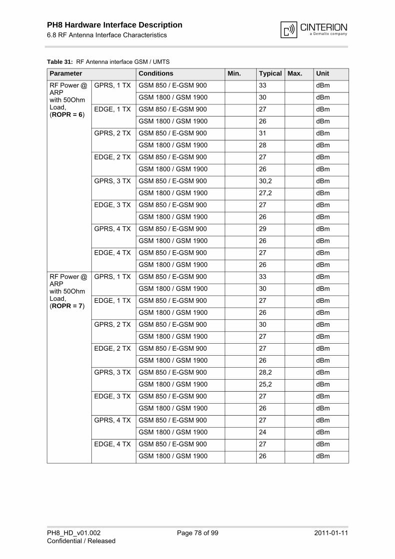
PH8 Hardware Interface Description6.8 RF Antenna Interface Characteristics81
PH8_HD_v01.002 Page 78 of 99 2011-01-11Confidential / Released
RF Power @ ARPwith 50Ohm Load,(ROPR = 6)
GPRS, 1 TX GSM 850 / E-GSM 900 33 dBm
GSM 1800 / GSM 1900 30 dBm
EDGE, 1 TX GSM 850 / E-GSM 900 27 dBm
GSM 1800 / GSM 1900 26 dBm
GPRS, 2 TX GSM 850 / E-GSM 900 31 dBm
GSM 1800 / GSM 1900 28 dBm
EDGE, 2 TX GSM 850 / E-GSM 900 27 dBm
GSM 1800 / GSM 1900 26 dBm
GPRS, 3 TX GSM 850 / E-GSM 900 30,2 dBm
GSM 1800 / GSM 1900 27,2 dBm
EDGE, 3 TX GSM 850 / E-GSM 900 27 dBm
GSM 1800 / GSM 1900 26 dBm
GPRS, 4 TX GSM 850 / E-GSM 900 29 dBm
GSM 1800 / GSM 1900 26 dBm
EDGE, 4 TX GSM 850 / E-GSM 900 27 dBm
GSM 1800 / GSM 1900 26 dBm
RF Power @ ARPwith 50Ohm Load,(ROPR = 7)
GPRS, 1 TX GSM 850 / E-GSM 900 33 dBm
GSM 1800 / GSM 1900 30 dBm
EDGE, 1 TX GSM 850 / E-GSM 900 27 dBm
GSM 1800 / GSM 1900 26 dBm
GPRS, 2 TX GSM 850 / E-GSM 900 30 dBm
GSM 1800 / GSM 1900 27 dBm
EDGE, 2 TX GSM 850 / E-GSM 900 27 dBm
GSM 1800 / GSM 1900 26 dBm
GPRS, 3 TX GSM 850 / E-GSM 900 28,2 dBm
GSM 1800 / GSM 1900 25,2 dBm
EDGE, 3 TX GSM 850 / E-GSM 900 27 dBm
GSM 1800 / GSM 1900 26 dBm
GPRS, 4 TX GSM 850 / E-GSM 900 27 dBm
GSM 1800 / GSM 1900 24 dBm
EDGE, 4 TX GSM 850 / E-GSM 900 27 dBm
GSM 1800 / GSM 1900 26 dBm
Table 31: RF Antenna interface GSM / UMTS
Parameter Conditions Min. Typical Max. Unit

PH8 Hardware Interface Description6.8 RF Antenna Interface Characteristics81
PH8_HD_v01.002 Page 79 of 99 2011-01-11Confidential / Released
RF Power @ ARPwith 50Ohm Load,(ROPR = 8, i.e. maximum reduction)
GPRS, 1 TX GSM 850 / E-GSM 900 33 dBm
GSM 1800 / GSM 1900 30 dBm
EDGE, 1 TX GSM 850 / E-GSM 900 27 dBm
GSM 1800 / GSM 1900 26 dBm
GPRS, 2 TX GSM 850 / E-GSM 900 30 dBm
GSM 1800 / GSM 1900 27 dBm
EDGE, 2 TX GSM 850 / E-GSM 900 24 dBm
GSM 1800 / GSM 1900 23 dBm
GPRS, 3 TX GSM 850 / E-GSM 900 28,2 dBm
GSM 1800 / GSM 1900 25,2 dBm
EDGE, 3 TX GSM 850 / E-GSM 900 22,2 dBm
GSM 1800 / GSM 1900 21,2 dBm
GPRS, 4 TX GSM 850 / E-GSM 900 27 dBm
GSM 1800 / GSM 1900 24 dBm
EDGE, 4 TX GSM 850 / E-GSM 900 21 dBm
GSM 1800 / GSM 1900 20 dBm
1. Applies also to UMTS Rx diversity antenna.
Table 31: RF Antenna interface GSM / UMTS
Parameter Conditions Min. Typical Max. Unit
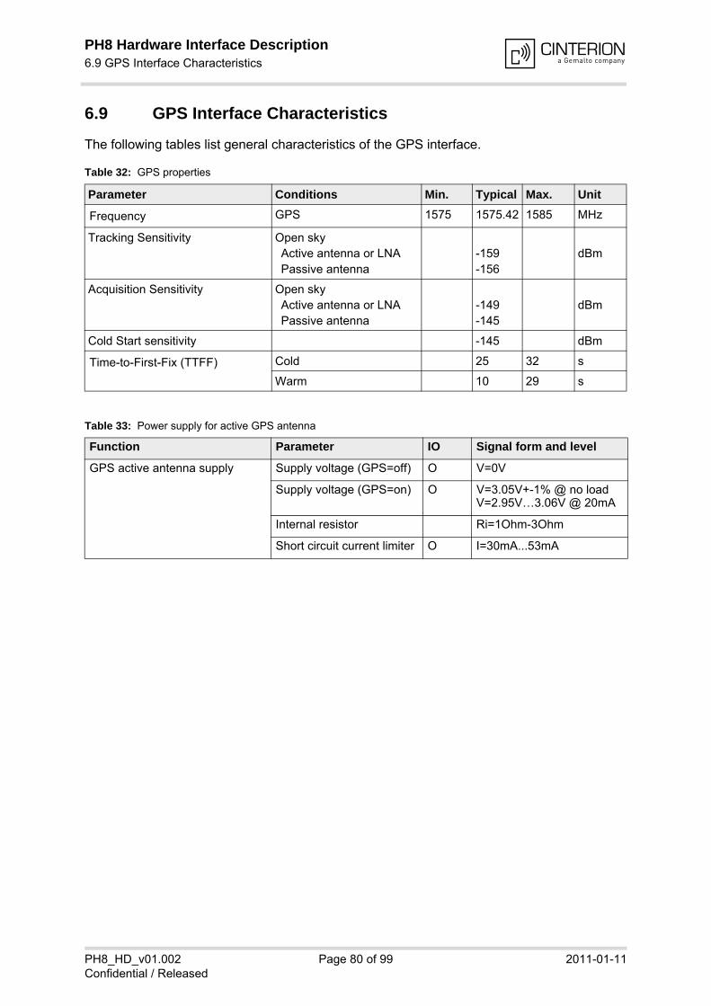
PH8 Hardware Interface Description6.9 GPS Interface Characteristics81
PH8_HD_v01.002 Page 80 of 99 2011-01-11Confidential / Released
6.9 GPS Interface Characteristics
The following tables list general characteristics of the GPS interface.
Table 32: GPS properties
Parameter Conditions Min. Typical Max. Unit
Frequency GPS 1575 1575.42 1585 MHz
Tracking Sensitivity Open skyActive antenna or LNAPassive antenna
-159 -156
dBm
Acquisition Sensitivity Open skyActive antenna or LNAPassive antenna
-149-145
dBm
Cold Start sensitivity -145 dBm
Time-to-First-Fix (TTFF) Cold 25 32 s
Warm 10 29 s
Table 33: Power supply for active GPS antenna
Function Parameter IO Signal form and level
GPS active antenna supply Supply voltage (GPS=off) O V=0V
Supply voltage (GPS=on) O V=3.05V+-1% @ no loadV=2.95V…3.06V @ 20mA
Internal resistor Ri=1Ohm-3Ohm
Short circuit current limiter O I=30mA...53mA

PH8 Hardware Interface Description6.10 Electrostatic Discharge81
PH8_HD_v01.002 Page 81 of 99 2011-01-11Confidential / Released
6.10 Electrostatic Discharge
The module is not protected against Electrostatic Discharge (ESD) in general. Consequently, it is subject to ESD handling precautions that typically apply to ESD sensitive components. Proper ESD handling and packaging procedures must be applied throughout the processing, handling and operation of any application that incorporates a PH8 module.
Special ESD protection provided on PH8:SIM/USIM interface: Serial resistor and clamp diodes for protection against overvoltage. All antenna interfaces: Inductor/capacitorBATT+: Inductor/capacitor
The remaining interfaces of PH8 are not accessible to the user of the final product (since they are installed within the device) and are therefore only protected according to the JEDEC JESD22-A114D requirements.
PH8 has been tested according to the following standards. The measured values can be gath-ered from the following table.
Note: Please note that the values may vary with the individual application design. For example, it matters whether or not the application platform is grounded over external devices like a com-puter or other equipment, such as the Cinterion Wireless Modules reference application de-scribed in Chapter 9.
Table 34: Measured electrostatic values
Specification / Requirements Contact discharge Air discharge
JEDEC JESD22-A114D
All board-to-board interfaces ± 1kV Human Body Model n.a.
ETSI EN 301 489-1/7
SIM/USIM interface ± 4kV ± 8kV
All antenna interfaces (GSM/UMTS/GPS)
± 4kV ± 8kV
BATT+ ± 4kV ± 8kV
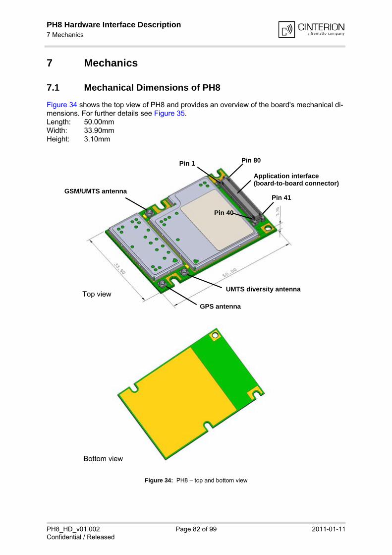
PH8 Hardware Interface Description7 Mechanics87
PH8_HD_v01.002 Page 82 of 99 2011-01-11Confidential / Released
7 Mechanics
7.1 Mechanical Dimensions of PH8
Figure 34 shows the top view of PH8 and provides an overview of the board's mechanical di-mensions. For further details see Figure 35. Length: 50.00mmWidth: 33.90mmHeight: 3.10mm
Figure 34: PH8 – top and bottom view
GSM/UMTS antenna
GPS antenna
UMTS diversity antenna
Pin 1 Pin 80
Pin 41
Pin 40
Top view
Bottom view
Application interface(board-to-board connector)

PH8 Hardware Interface Description7.1 Mechanical Dimensions of PH887
PH8_HD_v01.002 Page 83 of 99 2011-01-11Confidential / Released
Figure 35: Dimensions of PH8 (all dimensions in mm)

PH8 Hardware Interface Description7.2 Mounting PH8 to the Application Platform87
PH8_HD_v01.002 Page 84 of 99 2011-01-11Confidential / Released
7.2 Mounting PH8 to the Application Platform
There are many ways to properly install PH8 in the host device. An efficient approach is to mount the PH8 PCB to a frame, plate, rack or chassis.
Fasteners can be M2 screws plus suitable washers, circuit board spacers, or customized screws, clamps, or brackets. In addition, the board-to-board connection can also be utilized to achieve better support. To help you find appropriate spacers a list of selected screws and dis-tance sleeves for 3mm stacking height can be found in Section 10.2.
For proper grounding it is strongly recommended to use large ground plane on the bottom of board in addition to the five GND pins of the board-to-board connector. The ground plane may also be used to attach cooling elements, e.g. a heat sink or thermally conductive tape.
To prevent mechanical damage, be careful not to force, bend or twist the module. Be sure it is positioned flat against the host device. See also Section 10.3 with mounting advice sheet.
7.3 Board-to-Board Application Connector
This section provides the specifications of the 80-pin board-to-board connector used to connect PH8 to the external application.
Connector mounted on the PH8 module:
Type: 52991-0808 SlimStack Receptacle 80 pins, 0.50mm pitch, for stacking heights of3.0 or 4.0mm, see Figure 37 for details.
Supplier: Molex, http//www.molex.com

PH8 Hardware Interface Description7.3 Board-to-Board Application Connector87
PH8_HD_v01.002 Page 85 of 99 2011-01-11Confidential / Released
Mating connector types for the customer's application offered by Molex:
Figure 36: Mating board-to-board connector 53748-0808 on application
• 53748-0808 SlimStack Plug, 3mm stacking height, see Figure 38 for details.
• 53916-0808 SlimStack Plug, 4mm stacking height
Note: There is no inverse polarity protection for the board-to-board connector. It is therefore very important that the board-to-board connector is connected correctly to the host application, i.e., pin1 must be connected to pin1, pin2 to pin 2, etc. Pin assignments are listed in Section 6.5, pin locations are shown in Figure 34.
Table 35: Technical specifications of Molex board-to-board connector
Parameter Specification (80-pin B2B connector)
Electrical
Number of Contacts 80
Contact spacing 0.5mm (.020")
Voltage 50V
Rated current 0.5A max per contact
Contact resistance 50m max per contact
Insulation resistance > 100M
Dielectric Withstanding Voltage 500V AC (for 1 minute)
Physical
Insulator material (housing) White glass-filled LCP plastic, flammability UL 94V 0
Contact material Plating: Gold over nickel
Insertion force 1st < 74.4N
Insertion force 30th < 65.6N
Withdrawal force 1st > 10.8N
Maximum connection cycles 30 (@ 70m max per contact)

PH8 Hardware Interface Description7.3 Board-to-Board Application Connector87
PH8_HD_v01.002 Page 86 of 99 2011-01-11Confidential / Released
Figure 37: Molex board-to-board connector 52991-0808 on PH8
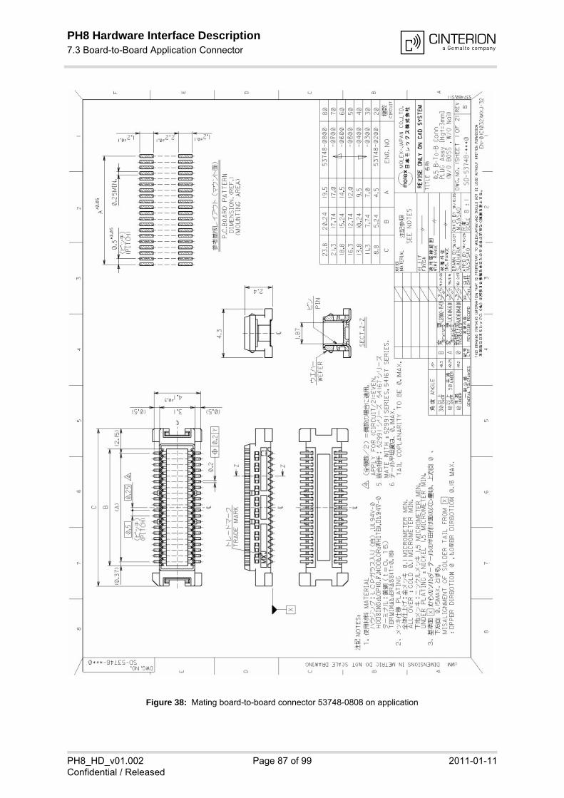
PH8 Hardware Interface Description7.3 Board-to-Board Application Connector87
PH8_HD_v01.002 Page 87 of 99 2011-01-11Confidential / Released
Figure 38: Mating board-to-board connector 53748-0808 on application

PH8 Hardware Interface Description8 Sample Application89
PH8_HD_v01.002 Page 88 of 99 2011-01-11Confidential / Released
8 Sample Application
Figure 39 shows a typical example of how to integrate an PH8 module with an application.
The audio interface demonstrates the balanced connection of microphone and earpiece. This solution is particularly well suited for internal transducers.
The PWR_IND line is an open collector that needs an external pull-up resistor which connects to the voltage supply VCC µC of the microcontroller. Low state of the open collector pulls the PWR_IND signal low and indicates that the PH8 module is active, high level notifies the Power-down mode.
If the module is in Power-down mode avoid current flowing from any other source into the mod-ule circuit, for example reverse current from high state external control lines. Therefore, the controlling application must be designed to prevent reverse flow. If an external level controller is required, this can be done by using for example a 5V I/O tolerant buffer/driver like a "74AVC4T245" with OE (Output Enable) controlled by PWR_IND.
The EMC measures are best practice recommendations. In fact, an adequate EMC strategy for an individual application is very much determined by the overall layout and, especially, the po-sition of components.
Disclaimer:No warranty, either stated or implied, is provided on the sample schematic diagram shown in Figure 39 and the information detailed in this section. As functionality and compliance with na-tional regulations depend to a great amount on the used electronic components and the indi-vidual application layout manufacturers are required to ensure adequate design and operating safeguards for their products using PH8 modules.

PH8 Hardware Interface Description8 Sample Application89
PH8_HD_v01.002 Page 89 of 99 2011-01-11Confidential / Released
Figure 39: PH8 sample application

PH8 Hardware Interface Description9 Reference Approval91
PH8_HD_v01.002 Page 90 of 99 2011-01-11Confidential / Released
9 Reference Approval
9.1 Reference Equipment for Type Approval
The Cinterion Wireless Modules reference setup submitted to type approve PH8 is shown in the following figure1. The module is connected to the DSB75 via a special adapter and either mounted directly onto the adapter or connected using a flex cable:
Figure 40: Reference equipment for type approval
1. For RF performance tests a mini-SMT/U.FL to SMA adapter with attached 6dB coaxial attenuator is cho-sen to connect the module directly to the GSM/UMTS/GPS test equipment instead of employing the SMAantenna connectors on the PH8-DSB75 adapter as shown in Figure 40. The following products arerecommended: Hirose SMA-Jack/U.FL-Plug conversion adapter HRMJ-U.FLP(40)(for details see see http://www.hirose-connectors.com/ or http://www.farnell.com/Aeroflex Weinschel Fixed Coaxial Attenuator Model 3T/4T (for details see http://www.aeroflex.com/ams/weinschel/pdfiles/wmod3&4T.pdf)

PH8 Hardware Interface Description9.2 Compliance with FCC and IC Rules and Regulations91
PH8_HD_v01.002 Page 91 of 99 2011-01-11Confidential / Released
9.2 Compliance with FCC and IC Rules and Regulations
The Equipment Authorization Certification for the Cinterion Wireless Modules reference appli-cation described in Section 9.1 will be registered under the following identifiers:
FCC Identifier QIPPH8Industry Canada Certification Number: 7830A-PH8Granted to Cinterion Wireless Modules GmbH
Manufacturers of mobile or fixed devices incorporating PH8 modules are authorized to use the FCC Grants and Industry Canada Certificates of the PH8 modules for their own final products according to the conditions referenced in these documents. In this case, the FCC label of the module shall be visible from the outside, or the host device shall bear a second label stating "Contains FCC ID QIPPH8", and accordingly “Contains IC 7830A-PH8“.
IMPORTANT:Manufacturers of portable applications incorporating PH8 modules are required to have their final product certified and apply for their own FCC Grant and Industry Canada Certificate relat-ed to the specific portable mobile. This is mandatory to meet the SAR requirements for portable mobiles (see Section 1.3.1 for detail).
Changes or modifications not expressly approved by the party responsible for compliance could void the user's authority to operate the equipment.
Note: This equipment has been tested and found to comply with the limits for a Class B digital device, pursuant to part 15 of the FCC Rules. These limits are designed to provide reasonable protection against harmful interference in a residential installation. This equipment generates, uses and can radiate radio frequency energy and, if not installed and used in accordance with the instructions, may cause harmful interference to radio communications. However, there is no guarantee that interference will not occur in a particular installation. If this equipment does cause harmful interference to radio or television reception, which can be determined by turning the equipment off and on, the user is encouraged to try to correct the interference by one or more of the following measures: • Reorient or relocate the receiving antenna. • Increase the separation between the equipment and receiver. • Connect the equipment into an outlet on a circuit different from that to which the receiver
is connected. • Consult the dealer or an experienced radio/TV technician for help.

PH8 Hardware Interface Description10 Appendix99
PH8_HD_v01.002 Page 92 of 99 2011-01-11Confidential / Released
10 Appendix
10.1 List of Parts and Accessories
Table 36: List of parts and accessories
Description Supplier Ordering information
PH8 Cinterion Standard module Cinterion Wireless Modules IMEI:Ordering number: L30960-N1900-A100
Customer IMEI:Ordering number: L30960-N1905-A100
DSB75 Support Box Cinterion Ordering number: L36880-N8811-A100
DSB75-Adapter for mounting the PH8 module
Cinterion Ordering number: L30960-N1802-A100
Votronic Handset VOTRONIC Votronic HH-SI-30.3/V1.1/0VOTRONIC Entwicklungs- und Produktionsgesellschaft für elek-tronische Geräte mbHSaarbrücker Str. 866386 St. IngbertGermanyPhone: +49-(0)6 89 4 / 92 55-0Fax: +49-(0)6 89 4 / 92 55-88Email: [email protected]
SIM card holder incl. push button ejector and slide-in tray
Molex Ordering numbers: 91228 91236
Sales contacts are listed in Table 37.
Board-to-board connector Molex Sales contacts are listed in Table 37.
U.FL antenna connector Hirose or Molex Sales contacts are listed in Table 37 and Table 38.
PH8 Hardware Interface Description10.1 List of Parts and Accessories99
PH8_HD_v01.002 Page 93 of 99 2011-01-11Confidential / Released
Table 37: Molex sales contacts (subject to change)
MolexFor further information please click:http://www.molex.com
Molex Deutschland GmbHFelix-Wankel-Str. 114078 Heilbronn-BiberachGermanyPhone: +49-7066-9555 0Fax: +49-7066-9555 29Email: [email protected]
American HeadquartersLisle, Illinois 60532U.S.A.Phone: +1-800-78MOLEXFax: +1-630-969-1352
Molex China DistributorsBeijing, Room 1319, Tower B, COFCO PlazaNo. 8, Jian Guo Men Nei Street, 100005BeijingP.R. ChinaPhone: +86-10-6526-9628 Phone: +86-10-6526-9728 Phone: +86-10-6526-9731 Fax: +86-10-6526-9730
Molex Singapore Pte. Ltd.Jurong, SingaporePhone: +65-268-6868Fax: +65-265-6044
Molex Japan Co. Ltd.Yamato, Kanagawa, Japan Phone: +81-462-65-2324Fax: +81-462-65-2366
Table 38: Hirose sales contacts (subject to change)
Hirose Ltd.For further information please click: http://www.hirose.com
Hirose Electric (U.S.A.) Inc2688 Westhills CourtSimi Valley, CA 93065U.S.A.
Phone: +1-805-522-7958Fax: +1-805-522-3217
Hirose Electric GmbHHerzog-Carl-Strasse 473760 OstfildernGermany
Phone: +49-711-456002-1Fax: +49-711-456002-299Email: [email protected]
Hirose Electric UK, LtdCrownhill Business Centre22 Vincent Avenue, CrownhillMilton Keynes, MK8 OABGreat Britain
Phone: +44-1908-305400Fax: +44-1908-305401
Hirose Electric Co., Ltd.5-23, Osaki 5 Chome, Shinagawa-KuTokyo 141Japan
Phone: +81-03-3491-9741Fax: +81-03-3493-2933
Hirose Electric Co., Ltd. European BrancheFirst class Building 4FBeechavenue 461119PV Schiphol-RijkNetherlands
Phone: +31-20-6557-460Fax: +31-20-6557-469

PH8 Hardware Interface Description10.2 Fasteners and Fixings for Electronic Equipment99
PH8_HD_v01.002 Page 94 of 99 2011-01-11Confidential / Released
10.2 Fasteners and Fixings for Electronic Equipment
This section provides a list of suppliers and manufacturers offering fasteners and fixings for electronic equipment and PCB mounting. The content of this section is designed to offer basic guidance to various mounting solutions with no warranty on the accuracy and sufficiency of the information supplied. Please note that the list remains preliminary although it is going to be up-dated in later versions of this document.
10.2.1 Fasteners from German Supplier ETTINGER GmbH
Sales contact:ETTINGER GmbHhttp://www.ettinger.de/main.cfmPhone: +4981 04 66 23 – 0Fax: +4981 04 66 23 – 0
The following tables contain only article numbers and basic parameters of the listed compo-nents. For further detail and ordering information please contact Ettinger GmbH.
Please note that some of the listed screws, spacers and nuts are delivered with the DSB75 Support Board. See comments below.
Article number: 05.71.038 Spacer - Aluminum /Wall thickness = 0.8mm
Length 3.0mm
Material AlMgSi-0,5
For internal diameter M2=2.0-2.3
Internal diameter d = 2.4mm
External diameter 4.0mm
Vogt AG No. x40030080.10

PH8 Hardware Interface Description10.2 Fasteners and Fixings for Electronic Equipment99
PH8_HD_v01.002 Page 95 of 99 2011-01-11Confidential / Released
Article number: 07.51.403 Insulating Spacer for M2Self-gripping1
1. 2 spacers are delivered with DSB75 Support Board
Length 3.0mm
Material Polyamide 6.6
Surface Black
Internal diameter 2.2mm
External diameter 4.0mm
Flammability rating UL94-HB
Article number: 05.11.209 Threaded Stud M2.5 - M2 Type E /External thread at both ends
Length 3.0mm
Material Stainless steel X12CrMoS17
Thread 1 / Length M2.5 / 6.0mm
Thread 2 / Length M2 / 8.0mm
Width across flats 5
Recess yes
Type External / External
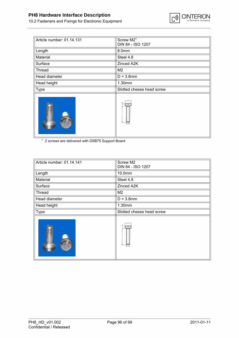
PH8 Hardware Interface Description10.2 Fasteners and Fixings for Electronic Equipment99
PH8_HD_v01.002 Page 96 of 99 2011-01-11Confidential / Released
Article number: 01.14.131 Screw M21 DIN 84 - ISO 1207
1. 2 screws are delivered with DSB75 Support Board
Length 8.0mm
Material Steel 4.8
Surface Zinced A2K
Thread M2
Head diameter D = 3.8mm
Head height 1.30mm
Type Slotted cheese head screw
Article number: 01.14.141 Screw M2DIN 84 - ISO 1207
Length 10.0mm
Material Steel 4.8
Surface Zinced A2K
Thread M2
Head diameter D = 3.8mm
Head height 1.30mm
Type Slotted cheese head screw

PH8 Hardware Interface Description10.2 Fasteners and Fixings for Electronic Equipment99
PH8_HD_v01.002 Page 97 of 99 2011-01-11Confidential / Released
Article number: 02.10.011 Hexagon Nut1
DIN 934 - ISO 4032
1. 2 nuts are delivered with DSB75 Support Board
Material Steel 4.8
Surface Zinced A2K
Thread M2
Wrench size / Ø 4
Thickness / L 1.6mm
Type Nut DIN/UNC, DIN934
PH8 Hardware Interface Description10.3 Mounting Advice Sheet99
PH8_HD_v01.002 Page 98 of 99 2011-01-11Confidential / Released
10.3 Mounting Advice Sheet
To prevent mechanical damage, be careful not to force, bend or twist the module. Be sure it is positioned flat against the host device (see also Section 7.2). The advice sheet on the next page shows a number of examples for the kind of bending that may lead to mechanical damage of the module.
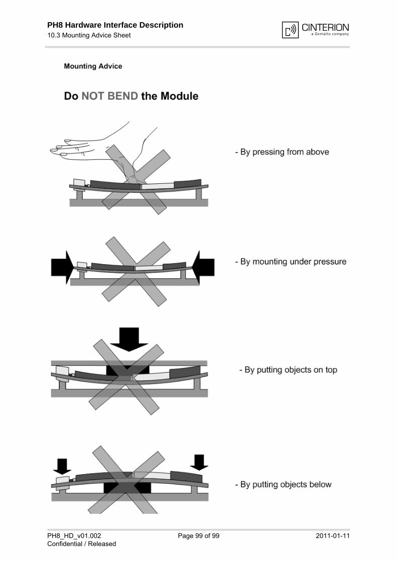
PH8 Hardware Interface Description10.3 Mounting Advice Sheet99
PH8_HD_v01.002 Page 99 of 99 2011-01-11Confidential / Released