components, packaging, and manufacturing technology ... · components, packaging and manufacturing...
TRANSCRIPT
1Fall 2012 IEEE CPMT Society Newsletter
NEWSLETTER SUBMISSION DEADLINES:
1 December 2012 for Winter issue1 February 2013 for Spring issue
1 May 2013 for Summer issue1 August 2013 for Fall issue
Submit all material to [email protected]
Components, Packaging,and Manufacturing Technology Society Newsletter
THE GLOBAL SOCIETY FOR MICROELECTRONICS SYSTEMS PACKAGING
VOL. 35 NO. 3, FALL 2012, ISSN 1077-2999 cpmt.ieee.org
More Value From Your CPMT Membership
Your IEEE Components, Packaging and Manufacturing
Technology (CPMT) Society membership will give you
more value than ever in the coming year.
When you renew for 2013, your CPMT membership (US$15;
Students US$8) will include an electronic subscription to IEEE Transactions on Components, Packaging and Manufacturing Technology, published monthly.
You can also add a print subscription to IEEE Transactions on Components, Packaging and Manufacturing Technology.
If you are interested in adding a print subscription to IEEE Transactions on Components, Packaging and Manufacturing Technology for US$25 ($13 for students) as you renew, sign in
with your IEEE Account. Once signed it, a page will present
that includes your contact information, and all 2012 member-
ships and subscriptions. On this page is the Membership Media
Options section. In that section, click “edit” under IEEE Com-
ponents, Packaging and Manufacturing Technology Society
Membership and a box will pop up. Simply click the check-
boxes to opt in and opt out of possible subscription options, and
click “Save” to continue.
If you plan to renew your membership by mailing back your
printed invoice, and wish to receive the print version of IEEE Transactions on Components, Packaging and Manufacturing Technology, simply write “IEEE Transactions on Components, Packaging and Manufacturing Technology Print” on the printed
invoice, and add US$25 (US$13 for students) to the total bill.

2 IEEE CPMT Society Newsletter Fall 2012
CPMT OfficersPresident: S-W. Ricky Lee [email protected]
VP (Technical): Jie Xue [email protected]
VP (Conferences): Jean Trewhella [email protected]
VP (Publications): R. Wayne Johnson [email protected]
VP (Education): Kitty Pearsall [email protected]
VP (Finance): Thomas G. Reynolds III [email protected]
Sr. Past Pres.: William T. Chen [email protected]
Jr. Past Pres.: Rolf Aschenbrenner Rolf.Aschenbrenner@izm.
fraunhofer.de
Executive Director: Marsha Tickman [email protected]
Elected Board Members2012: Chris Bailey, Daniel Donahoe, Paul D. Franzon, Daniel Lu,
Kwang-Lung Lin, and Leonard W. Schaper
2013: Debendra Mallik, Toni Mattila, James E. Morris, Eric Perfecto,
Gilles Poupon, Dongkai Shangguan
2014: Masahiro Aoyagi, Avram Bar-Cohen, Darvin R. Edwards, Beth Keser,
Mervi Paulasto-Kröckel, CP Wong
CPMT Society NewsletterEditor-in-Chief: Kitty Pearsall [email protected]
CPMT Archival PublicationsTransactions on Components, Packaging and Manufacturing Technology
Managing Editor:R. Wayne Johnson
Co-Editor, Advanced Packaging:Ravi Mahajan
Co-Editor, Electrical Performance:José E. Schutt-Ainé
Co-Editor, Components: Characterization and Modeling:Koneru Ramakrishna
Co-Editor, Packaging Technologies:Kuo-Ning Chiang
Co-Editor, Electronics Manufacturing:R. Wayne Johnson
Technical Committee ChairsInterconnect & Substrate:Kishio Yokouchi
Materials & Processes:Rajen Chanchani
Nanotechnology:James Morris
RF & THz Devices:Craig Gaw
Energy Electronics:Douglas Hopkins
Electrical Design, Modeling & Simulation:Madhavan Swaminathan
Green Electronics:Nils Nissen
Thermal & Mechanical:Tony Mak
3D/TSV:Paul Franzon
Emerging Technologies:Erik Jung
Photonics – Communication, Sensing, Lighting:Tolga Tekin
Strategic Program DirectorsGlobal Chapters and Membership: Eric Perfecto, [email protected]
Student Programs: Chris Bailey, [email protected]
Industry Programs: Phil Garrou, pgarrou/[email protected]
Region 8 Programs: Toni Mattila, [email protected]
Region 10 Programs: Kwang-Lung Lin, [email protected]
Standing Committee ChairsAwards: Patrick Thompson, [email protected]
Fellows Evaluation: CP Wong, [email protected]
Long Range / Strategic Planning: William Chen, [email protected]
Nominations: Rolf Aschenbrenner, [email protected]
Distinguished LecturersProgram Director: Kitty Pearsall, [email protected]
Lecturers: Avram Bar-Cohen, Ph.D., H. Anthony Chan, Ph.D., Rajen Chanchani,
Ph.D., William T. Chen, Ph.D., Badih El-Kareh, Ph.D., Xuejun Fan, Ph.D., Paul D.
Franzon, Ph.D., Philip Garrou, Ph.D., George G. Harman, Ph.D., R. Wayne
Johnson, Ph.D., George A. Katopis, Ph.D., John H. Lau, Ph.D., Michael Lebby,
Ph.D, Ning-Cheng Lee, Ph.D., S. W. Ricky Lee, Ph.D., Johan Liu, Ph.D., James E.
Morris, Ph.D., Kyung W. Paik, Ph.D., T. Paul Parker, Michael Pecht, Ph.D., Karl J.
Puttlitz, Ph.D., Bahgat Sammakia, Ph.D., Dongkai Shangguan, Ph.D., Nihal
Sinnadurai, Ph.D., Ephraim Suhir, Ph.D., Yong-Khim Swee, Yutaka Tsukada,
Ph.D., Rao Tummala, Ph.D., Walter Trybula, Ph.D., E. Jan Vardaman, Paul
Wesling, CP Wong, Ph.D., Ralph W. Wyndrum Jr., Ph.D., Kishio Yokouchi, Ph.D.
Chapters and Student BranchesRefer to cpmt.ieee.org for CPMT Society Chapters and Student Branches list
IEEE Components, Packaging, and Manufacturing Technology Society Newsletter
is published quarterly by the Components, Packaging, and Manufacturing Technol-
ogy Society of the Institute of Electrical and Electronics Engineers, Inc. Headquar-
ters: 3 Park Avenue, 17th Floor, New York, NY 10016-5997. US $1.00 per member
per year is included in Society fee for each member of the Components, Packaging,
and Manufacturing Technology Society. Printed in U.S.A. Periodicals postage paid
at New York, NY, and at additional mailing offices. Postmaster: Send address
changes to IEEE CPMT Newsletter, IEEE 445 Hoes Lane, Piscataway, NJ 08854.
All rights reserved, copyright (c) 2012 by the CPMT Society of IEEE. Authors and
Artists given full permission for further use of their contributions. For circulation
information call IEEE Customer Service 800-701-4333, or FAX 908-981-9667.
IEEE prohibits discrimination, harassment, and bullying. For more information,visit http://www.ieee.org/web/aboutus/whatis/policies/p9-26.html.
Circulate your printed or PDF copy of this NEWSLETTER to co-workers.
3Fall 2012 IEEE CPMT Society Newsletter
President’s Column....
Cracking the Da Vinci Code of 3D-IC”? Sounds like the
title of a mystery film or novel. But this is the title of my
keynote presentation in a few recent CPMT-sponsored
conferences and symposiums, which revealed my view on 3D-IC.
With the aid of the PPT screen print above (instead of my regular
dull portrait, again), I would try to render the presentation and idea
to those who were not there……
Starting from the infancy of electronics, I presented the pictures
of two major milestones (at the upper-left corner), namely, the first
point-contact semiconductor transistor (1947, William Shockley,
Walter Brattain, John Bardeen) and the first integrated circuit (1958,
Jack Kilby). The third picture on the left showed the original sche-
matic drawing of Moore’s law (1965, Gordon Moore), followed by
the fourth picture below which exhibited the modified Moore’s law
for CPUs (1971–2011, Intel). In the ensuing four decades or so, the
microelectronics era basically followed the Moore’s law steadily.
At the turn of the century, some new concepts started to evolve.
The “Dumbo” flew from the lower-left corner across the slide to
represent the emergence of disruptive technologies. The diagram at
the upper-right corner is the famous ITRS figure for More Moore
(MM) and More than Moore (MtM). The vertical red axis indi-
cated the continuing trend of scaling, which actually implies “Min-
iaturization”. On the other hand, the horizontal blue axis exhibits
the emerging trend of “integration”. I intentionally capitalized the
former for a certain purpose later.
There exist several enabling technologies for MtM. Among
them, the most well-known one is probably through-silicon vias
(TSV), which was illustrated by the picture at the lower-right cor-
ner in the above slide. In the past few years, the concept of TSV has
been expanded to through-glass vias (TGV) and through-mold vias
(TMV) as shown in the two photos above the TSV, respectively.
Subsequently, some people suggested the term of “TSV” be gen-
eralized to “TxV”. In my humble opinion, no technologies could
become successful if they are not cost effective. Therefore, I further
recommended the terminology be modified to “T$V”, as depicted
at the top of the slide.
Now here comes the critical step. Let’s put the first letter of “Min-
iaturization” and that of “integration” together to form “Mi”. In the
musical scale, “Mi” is the third note, after “Do” and “Re”. In other
words, “Mi” represents “3”. Then the Dollar sign in “T$V” at the top
may drop down and stay next to “3”. This is how I deduced “3D” from
“MM”, “MtM”, and “TSV”. In order to make sure the audience got
the idea, I then posed the question: “Did you see that?” The answer
must be “I see”. Otherwise, I would re-run the slide over and over
again…… In case you still don’t get it, you may consider “IC” as the
acronym for IEEE CPMT.
This is how I cracked the Da Vinci code of 3D-IC from the per-
spective of packaging trends. Q.E.D. (quod erat demonstrandum)
I hope you enjoyed it!
Prof. S. W. Ricky Lee, IEEE Fellow, PresidentIEEE CPMT Society, Hong Kong University of Science and Technology, Kowloon, Hong Kong,
“
(Pictures extracted from various web sources)

4 IEEE CPMT Society Newsletter Fall 2012
CPMT Society Welcomes New and Returning Members
The Members listed below either joined or rejoined the CPMT Society between 1 August and 17 October 2012. Join us in welcoming
them to the CPMT Community.
Harold Arbelaez Duque Colombia Section Jun Li Santa Clara Valley Section
Jung Hyung Bae Seoul Section Bruce Lowther Northern Virginia Section
Jeanette Brooks Boise Section Christopher Mazique Atlanta Section
Alan Brownell Charlotte Section James Nadolny Susquehanna Section
Kihun Chang San Diego Section Zainal Abidin Nordin Malaysia Section
Daniel Deisz Northern Virginia Section Stefano Oggioni Italy Section
Robin Dykstra New Zealand Central Section Kenny Otiaba U.K. & Rep Of Ireland Section
Weileun Fang Taipei Section Michael Rattner San Francisco Section
Michel Fleury Ottawa Section Cindi Rose Twin Cities Section
Bih Wen Fon Malaysia Section Max Schneiderman Miami Section
Robert Gardyne Oakland-East Bay Section Ramya Shankar Santa Clara Valley Section
Gary Grimm Seattle Section Robert Sokolovskij Benelux Section
Paul Jacob Santa Clara Valley Section Venkatasubramanian Srinivasan Madras Section
Dennis Kehl West Michigan Section Ken-Ichi Takeda Tokyo Section
Ling Eng Khoong Singapore Section Rui Victal Toronto Section
Kati Kokko Benelux Section David Williams West Michigan Section
Christopher Laplante Denver Section Min-Feng Yu Atlanta Section
Call for Nominations for the 2013 CPMT Society Awards Nominations Due by January 31, 2012
The CPMT Society is full of highly talented professionals, and we have five awards to recognize those who have performed at an
exceptional level. Do you have a friend or colleague who has made outstanding contributions to the technical fields within CPMT?
Would you like him or her to receive recognition for these contributions? We would, too; you can make it happen by submitting a
nomination today.
The Awards Committee is currently accepting nominations for the 2013 CPMT Awards. All nomination packages are due by
January 31, 2013. Winners will be notified by April 15, 2013, and the awards will be presented at the 63rd Electronic Components
and Technology Conference, May 28–31, 2013, in Las Vegas, Nevada, USA. A current nomination form can be found on the
CPMT web site under the Awards link at: http://cpmt.ieee.org/awards.html. We look forward to receiving your nominations for
any of the awards described below.
CPMT Society offers the following awards for the purpose of recognizing outstanding service and contributions to the profes-
sional purposes of the CPMT Society.
CPMT Society News....
New IEEE CPMT Senior Members
Congratulations to the members listed below who were recently elevated to the grade of Senior Member.
The grade of Senior Member is the highest for which application may be made and shall require experience reflecting professional matu-
rity. For admission or transfer to the grade of Senior Member, a candidate shall be an engineer, scientist, educator, technical executive,
or originator in IEEE designated fields for a total of 10 years and have demonstrated 5 years of significant performance.
Individuals may apply for Senior Member grade online at: www.ieee.org/web/membership/senior-members/index.html
Dries Vande Ginste Vicente Gonzalez Millan HingWah Lee
Parthiban Arunasalam Kirk Gray Yuriy Shlepnev
Marie Cote Mike Hamilton Michael TÖpper

5Fall 2012 IEEE CPMT Society Newsletter
David Feldman Outstanding Contribution Award: To recognize outstanding contributions to the fields encompassed by the
CPMT Society through executive or managerial directions.
Prize: $2,500 and Certificate
Basis for Judging: Contributions to the organization or enterprises connected with the field, to CPMT Chapter, Section or
Board of Governors activities, and to the fields encompassed by the CPMT Society.
Eligibility: Recipient must have been a member of IEEE and CPMT for the past five (5) years, including 2012.
Outstanding Sustained Technical Contributions Award: To recognize outstanding sustained and continuing contributions to the
technology in fields encompassed by the CPMT Society.
Prize: $2,500 and Certificate
Basis for Judging: Technical contributions must be sustained and continuing over a period of at least five (5) and preferably
10 years. One major contribution will not qualify. Contributions must be documented by open literature publications such as
papers, patents, books and reports (available to the public).
Eligibility: Must have been a member of the IEEE and CPMT Society for the past three (3) years, including 2012.
Electronics Manufacturing Technology Award: To recognize major contributions to Electronic Manufacturing Technology in
fields encompassed by the CPMT Society.
Prize: $2,500 and Certificate
Basis for Judging: Contributions may include technical development of, or management (directing) of major new electronic
manufacturing processes; significantly increasing yield and/or reliability of established manufacturing processes, etc. Work in
the management of CPMT conferences or its BoG may be contributory but not sufficient to receive the award.
Eligibility: No need to be a member of IEEE and CPMT Society.
Exceptional Technical Achievement Award: To recognize an individual, or group of individuals (no more than three), for excep-
tional technical achievement in the fields encompassed by the CPMT Society.
Prize: $2,500 and a Certificate.
Basis for Judging: Technical contributions of the nominee(s) must be such that they are considered to be exceptional, not achieved
by most members. A single major contribution will qualify for this award. The contribution could be a significant invention, introduc-
tion of a significantly new and important technology or product (in which case, the nominee may be a team leader), or significant
work that advances the state-of-the-art in CPMT’s field of interest. The technical contributions must be documented by open litera-
ture publications such as papers, patents, books, and reports (available to the public). Technical recognition and awards from the
organization employing the individual as well as awards from other IEEE and non-IEEE technical societies may also be contributory.
Eligibility: Recipient(s) must have been a member of IEEE and CPMT for the past three (3) years, including 2012. There are
no requirements for service to the IEEE or CPMT Society.
Outstanding Young Engineer Award: To recognize outstanding contributions to the fields encompassed by the CPMT Society
through invention, technical development, publications, or new product implementation.
Prize: $1,500 and Certificate
Basis for Judging: Technical contributions through patent invention, contributions to technology or product development
within the CPMT Field of Interest. May encompass management (directing) of significant new product introduction or imple-
mentation of major new electronic manufacturing processes; significantly increasing yield and/or reliability of established
manufacturing processes. Contributions to the Society, through the BoG, Conferences, Chapters, etc., will also be considered.
Proof of contributions may consist of open literature publications (preferred) such as papers, patents, books, and reports (avail-
able to the public). At least three (3) letters from peers and management at the nominee’s place of employment attesting to the
accomplishment(s) can be accepted in lieu of publications.
Eligibility: Must have been a member of the IEEE and CPMT (member grade or above) for the past three (3) years, including
2012, and must be 35 years of age, or younger, on December 31, 2012.
Guidelines for Nominators:• Past recipients of an award are not eligible to receive that same award. For lists of past awardees, see http://cpmt.ieee.org/
awards.html
• An individual may submit only one nomination per award but may submit nominations for more than one award.
• It is the responsibility of the nominator to provide quality documentation to assist the Awards Committee in evaluating the candidate.
• Please send nominations to CPMT Society Awards Committee Chair by e-mail (preferred) or mail:
Patrick ThompsonTexas Instruments
13020 TI Blvd, MS3521, Dallas, TX 75243, [email protected]
6 IEEE CPMT Society Newsletter Fall 2012
IEEE CPMT UK&RI ChapterResearch to Industry (R2i) Workshop, 19th June 2012 at
Henry Ford Centre, Loughborough, UKSubmitted by Nihal Sinnadurai, Chair IEEE CPMT UK&RI
The objective of R2i was to provide an opportunity for
industry take-up of good developmental research. The ini-
tiative was sponsored jointly by IEEE, IMAPS-UK and the
UK’s IeMRC (electronics manufacturing research centre). A very
disciplined programme was arranged. A template was created for
the sessions and presentations. The programme comprised 4 ses-
sions, each led by a relevant Keynote practitioner or government
funding representative, such as those listed below.
The National Microelectronics Institute (NMI) gave an over-
view of the mechanisms that were available for the funding of
research projects, the pathways and requirements. The huge range
of potential funding routes was also outlined.
The Knowledge Transfer Partnerships (KTP), managed by the
Technology Strategy Board. KTPs were described as a mechanism
for providing a commercial pull to research carried out at Uni-
versities. KTP projects typically lasted from 6 months to 3 years,
with 2 years being the preferred duration. The associate worker
on a KTP project would be jointly recruited but employed by the
knowledge base partner and typically located at the business prem-
ises. KTPs required innovative projects with a strategic relevance
to the business and that had a clear knowledge transfer element
creating a step change in capability.
The IeMRC director spoke on “The journey of a successful
project”—outlining some of the key challenges of taking research
up the technology readiness levels towards commercial imple-
mentation. The UK government has acknowledged the need to get
more of the UK’s successful research into industry, where its ben-
efits could be utilised and he cited, by way of example, the recent
announcement of substantial funding to support the development
of graphene in the UK.
The presenter from the Centre for Process Innovation (CPI)
addressed electronics capability in the High Value Manufactur-
ing Catapult Centre. Two influential reports by James Dyson
and Herman Hauser had highlighted the problems of getting
new technology to market. The Catapult Centres were aimed at
bridging the gap (the valley of death) between academia and
industry take-up.
At each session, the Researchers presented their results in tight
5-minute slots before an audience which included industry play-
ers. The aim was to stimulate take-up of the research by industrial-
ists and venture funders to lead to development, manufacture and
the market.
IEEE UK&RI takes a strong interest in good research. At the
R2i event we praised the good research and rec-
ognised outcomes that were worthy of take-up
from industry.
As an example of research en-route to
industry take-up, Liudi’s research on MEMS
application of carbon nanotubes to fabri-
cate advanced electrical contacts for MEMS
switches capable of switching >10 mA at up
to 4 V over >108 cycles. MEMS switch/relays
had been forecast to be a multibillion dollar
technology area but technical barriers were the
lack of switches and the need for high conduc-
tivity, reliability and long lifetimes. The reli-
ability work indicated that CNT based devices
could provide extended switching cycles com-
pared with more conventional switching, that
it was possible to switch 20 mA at 4 V for
more than > 80 million cycles.
The R2i event was well attended by research-
ers but more venture participation was needed.
We will try the event again in 2013.
Chapter News....
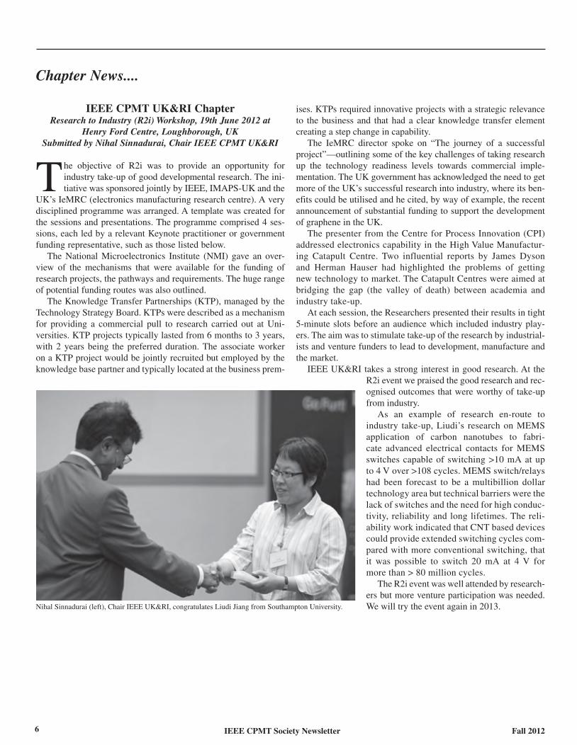
Nihal Sinnadurai (left), Chair IEEE UK&RI, congratulates Liudi Jiang from Southampton University.
7Fall 2012 IEEE CPMT Society Newsletter
CPMT Transactions Offers Open Access Publishing Option
The IEEE Transactions on Components, Packaging and Manufacturing Technology offers its authors the option to
publish articles either for Traditional publication or for
Open Access (OA) publication.
The majority of IEEE Transactions operate according to this
model and are known as hybrid journals.
The Traditional manuscript option is a continuation of the long-
standing approach in which published articles are available to all
qualified subscribers and purchasers via IEEE Xplore. Authors
only pay fees for overlength pages, if applicable or for color
images in print, if they choose this option.
The OA option enables unrestricted public access to the article
via IEEE Xplore. The OA option will be offered to the author at the
time the article is submitted for review. If selected, the author must
pay the OA fee (discounted rate of US$1750 per article) before the
article is published in the Transactions.
The IEEE peer review standard of excellence is applied consist-
ently to all submissions. All accepted articles will be included in
the print issue mailed to those who subscribe to print.
Publication News....
Learn more about IEEE Open Accesswww.ieee.org/open-access
IEEE Open AccessXplore®

8 IEEE CPMT Society Newsletter Fall 2012
Have You Read Them? The Most Downloaded CPMT Transactions Papers
What might you be missing in the CPMT literature?
Following is a list of most downloaded papers from the
Transactions on Components, Packaging and
Manufacturing Technology in Third Quarter 2012. Subscribers can
access these and other papers in IEEE Xplore (http://ieeexplore.
ieee.org/xpl/RecentIssue.jsp?punumber=5503870#).
A Compact and Embedded Balanced Bandpass Filter With Wideband Common-Mode Suppression on Wireless SiP
Hung-Chuan Chen; Chung-Hao Tsai; Tzong-Lin Wu; Vol-
ume: 2, Issue: 6, Publication Year: 2012, Page(s): 1030–1038
A compact balanced bandpass filter is proposed using a novel
circuit topology, which includes a differential resonator and a
common resonator in the conventional quasi-lumped coupled-line
circuit, instead of adopting quarter-wavelength or half-wavelength
transmission lines in the filter design. Based on this circuit topol-
ogy, the balanced bandpass filter can support bandpass filtering
function under differential-mode operation and exhibit bandstop
filtering function under common-mode noise. By employing the
advantage of the low-temperature co-fired ceramic fabrication
technology, a compact balanced bandpass filter is centered at
3.42 GHz with fractional bandwidth 10.4% for differential sig-
nals and rejection band is from 1.48 to 7.4 GHz for the common-
mode noise. Moreover, the proposed filter is able to introduce
a transmission zero with excellent common-mode suppression
(>;40 dB) within the differential-mode passband. The electrical
size of this filter is 5.6 × 5.4 mm with the corresponding electri-
cal size 0.113 × 0.109 mg, where mg is the guided wavelength at
the center frequency 3.42 GHz. This compact balanced bandpass
filter is suitable to be applied to the system-in-package technology
for wireless application.
Embedded Module for 3-D Mechanical Strain MeasurementMoore, L.; Barrett, J.; Volume: 2, Issue: 6, Publication Year:
2012, Page(s): 1002–1011
This paper presents the development and evaluation of
a miniature (1 cm3) embedded electronic module that can
resolve temperature-compensated mechanical strain in three
dimensions. The module is designed to be embedded into
materials and to measure, in-situ, all nine components of strain
and to relay the information back to a PC via wired commu-
nications. The module can also be assembled as a component
in a “parent” encapsulated electronic system and interface
with the system’s digital bus. The module comprises three
miniature, off-the-shelf, three-gauge, rectangular rosettes
that are assembled in a 3-D array so that all components of
strain can be resolved. The module format is a cube, with
the gauges on the outer faces of the cube, and the electronics
on the inside. The electronics consists of signal conditioning
circuitry, a 24-bit sigma-delta ADC, a microcontroller which
sends the digital data directly to a master device such as PC,
and an onboard temperature sensor for thermal compensa-
tion of the gauges. The module was evaluated by encapsulat-
ing it in epoxy and subjecting it to compressive and tensile
testing in a mechanical tester. The results were compared to
finite element simulations with an average of 7% difference
between magnitudes and a standard deviation of 4%. Thermal
evaluation of the module was also carried out by subjecting
the test pieces to thermal loads and monitoring the response
of the system. The module is believed to be the smallest yet
reported self-contained, embedded system capable of resolv-
ing all components of 3-D strain, it is small enough to be
embedded in a wide range of materials and structures without
significant impact on the mechanical properties of its host.
It can, therefore, be used in applications such as structural
health monitoring and reliability prognostics and for calibra-
tion of mechanical/thermo-mechanical simulations.
High-Frequency Scalable Electrical Model and Analysis of a Through Silicon Via (TSV)
Joohee Kim; Jun So Pak; Jonghyun Cho; Eakhwan Song; Jeon-
ghyeon Cho; Heegon Kim; Taigon Song; Junho Lee; Hyungdong
Lee; Kunwoo Park; Seungtaek Yang; Min-Suk Suh; Kwang-Yoo
Byun; Joungho Kim; Volume: 1, Issue: 2, Publication Year: 2011,
Page(s): 181–195
We propose a high-frequency scalable electrical model of a
through silicon via (TSV). The proposed model includes not only
the TSV, but also the bump and the redistribution layer (RDL),
which are additional components when using TSVs for 3-D inte-
grated circuit (IC) design. The proposed model is developed with
analytic RLGC equations derived from the physical configuration.
Each analytic equation is proposed as a function of design param-
eters of the TSV, bump, and RDL, and is therefore, scalable. The
scalability of the proposed model is verified by simulation from
the 3-D field solver with parameter variations, such as TSV diam-
eter, pitch between TSVs, and TSV height. The proposed model
is experimentally validated through measurements up to 20 GHz
with fabricated test vehicles of a TSV channel, which includes
TSVs, bumps, and RDLs. Based on the proposed scalable model,
we analyze the electrical behaviors of a TSV channel with design
parameter variations in the frequency domain. According to the
frequency-domain analysis, the capacitive effect of a TSV is domi-
nant under 2 GHz. On the other hand, as frequency increases over 2
GHz, the inductive effect from the RDLs becomes significant. The
frequency dependent loss of a TSV channel, which is capacitive
and resistive, is also analyzed in the time domain by eye-diagram
measurements. Due to the frequency dependent loss, the voltage
and timing margins decrease as the data rate increases.
Characterization of Heat Dissipation From a Microprocessor Chip Using Digital Interferometry
Sajith, V.; Sobhan, C.B.P.; Volume: 2, Issue: 8, Publication
Year: 2012, Page(s): 1298–1306
Electronic circuit boards of computers consist of components
which generate substantial amounts of heat during their operation.
Among these, the microprocessor chip is one of the major sources
of heat generation. In high-performance processor chips, the rates
of heat generation are also correspondingly high. The performance
of the chips themselves, as well as that of the neighboring elec-
tronic components are affected by the temperature levels attained,
which in turn depend on the heat dissipation capability. Effec-
tive thermal management of microprocessor chips, following pre-
cise thermal characterization, is essential to avoid their untimely

9Fall 2012 IEEE CPMT Society Newsletter
failure due to overheating. The selection of an appropriate cooling
methodology and the design of an efficient cooling system for
the microprocessor chip essentially require a clear knowledge of
the heat dissipation rates during its operation. A comprehensive
database of heat dissipation from microprocessor chips as a func-
tion of the activity level, based on actual measurements, is rare to
find in the literature. A major reason for this is that conventional
intrusive measurements on and around the chip are quite insuf-
ficient, as they will alter the performance, while the system is
under operation. To overcome this, a nonintrusive digital inter-
ferometric measurement has been devised in this paper for obtain-
ing the in situ temperature distributions and the heat dissipation
patterns around the microprocessor chip, while it is under opera-
tion. The interferometric method utilizes interference of coherent
laser beams to make measurements in the thermal field around
the heat-dissipating component. An Intel Pentium 4 microproces-
sor with its integrated heat sink was used for experimentation.
The computational load on the processor was varied utilizing a
software package, thus varying the heat generation rates, and the
base temperature of the fins in the heat sink attached to the micro-
processor. Interferometric measurements were made to obtain the
temperature distribution in the medium, and the patterns of heat
dissipation from the fins’ surfaces. Indicators of the heat transfer
behavior, namely, the local heat flux values and the heat trans-
fer coefficients were obtained from the experiments, using digital
image processing techniques. Experiments were conducted at var-
ious fin-base temperatures, under free and forced convection con-
ditions, to characterize the effect through a database of the heat
dissipation level. In essence, a nonintrusive temperature measure-
ment method coupled with digital image processing techniques
has been successfully used for convective heat transfer studies on
the microchip while the microchip is under operation.
Affordable Ink-Jet Printed Antennas for RFID ApplicationsPranonsatit, S.; Worasawate, D.; Sritanavut, P.; Volume: 2,
Issue: 5; Publication Year: 2012, Page(s): 878–883
With the increasing demands of radio-frequency identification
(RFID) applications, an alternative ink-jet printing technique for
RFID tag antenna is demonstrated. Commercially available ink-jet
printers are adapted for conductive printing, in order to minimize
manufacturing cost. Paper-based dipole antenna and dipole with
a tuning stub antenna were designed. The antennas were ink-jet
printed and assembled with RFID chips. The performances of the
fabricated tags were measured through the reading range. With
reference to equivalent isotropically radiated power of 4 W at
923 MHz, the reading range of tag with dipole antenna is around
9 m and of tag with dipole with a tuning stub is nearly 13 m. These
performances are comparable to those of commercial tags. The
advantages of the proposed printing technique are simplicity, flex-
ibility and, more importantly, affordability. The technique can, in
addition, contribute to further development and enhance extension
of RFID applications.
PDN Impedance Modeling and Analysis of 3D TSV IC by Using Proposed P/G TSV Array Model Based on Separated P/G TSV and Chip-PDN Models
Jun So Pak; Joohee Kim; Jonghyun Cho; Kiyeong Kim; Taigon
Song; Seungyoung Ahn; Junho Lee; Hyungdong Lee; Kunwoo
Park; Joungho Kim; Volume: 1, Issue: 2; Publication Year: 2011,
Page(s): 208–219
The impedance of a power-distribution network (PDN) in
three-dimensionally stacked chips with multiple through-silicon-
via (TSV) connections (a 3D TSV IC) was modeled and analyzed
using a power/ground (P/G) TSV array model based on separated
P/G TSV and chip-PDN models at frequencies up to 20 GHz. The
proposed modeling and analysis methods for the P/G TSV and
chip-PDN are fundamental for estimating the PDN impedances
of 3D TSV ICs because they are composed of several chip-PDNs
and several thousands of P/G TSV connections. Using the pro-
posed P/G TSV array model, we obtained very efficient analy-
ses and estimations of 3D TSV IC PDNs, including the effects
of TSV inductance and multiple-TSV inductance, depending on
P/G TSV arrangement and the number of stacked chip-PDNs of
a 3D TSV IC PDN. Inductances related to TSVs, combined with
chip-PDN inductance and capacitance, created high upper peaks
of PDN impedance, near 1 GHz. Additionally, the P/G TSV array
produced various TSV array inductance effects on stacked chip-
PDN impedance, according to their arrangement, and induced
high PDN impedance, over 10 GHz.
Modeling and Analysis of Through-Silicon Via (TSV) Noise Coupling and Suppression Using a Guard Ring
Jonghyun Cho; Eakhwan Song; Kihyun Yoon; Jun So Pak;
Joohee Kim; Woojin Lee; Taigon Song; Kiyeong Kim; Junho Lee;
Hyungdong Lee; Kunwoo Park; Seungtaek Yang; Minsuk Suh;
Kwangyoo Byun; Joungho Kim; Volume: 1, Issue: 2; Publication
Year: 2011, Page(s): 220–233
In three-dimensional integrated circuit (3D-IC) systems that
use through-silicon via (TSV) technology, a significant design
consideration is the coupling noise to or from a TSV. It is impor-
tant to estimate the TSV noise transfer function and manage the
noise-tolerance budget in the design of a reliable 3D-IC system.
In this paper, a TSV noise coupling model is proposed based on
a three-dimensional transmission line matrix method (3D-TLM).
Using the proposed TSV noise coupling model, the noise trans-
fer functions from TSV to TSV and TSV to the active circuit
can be precisely estimated in complicated 3D structures, includ-
ing TSVs, active circuits, and shielding structures such as guard
rings. To validate the proposed model, a test vehicle was fabri-
cated using the Hynix via-last TSV process. The proposed model
was successfully verified by frequency- and time-domain mea-
surements. Additionally, a noise isolation technique in 3D-IC
using a guard ring structure is proposed. The proposed noise iso-
lation technique was also experimentally demonstrated; it pro-
vided –17 dB and –10 dB of noise isolation between the TSV and
an active circuit at 100 MHz and 1 GHz, respectively.
Wafer Bumping, Assembly, and Reliability of Fine-Pitch Lead-Free Micro Solder Joints for 3-D IC Integration
Ching-Kuan Lee; Tao-Chih Chang; Lau, J.H.; Yu-Jiau Huang;
Huan-Chun Fu; Jui-Hsiung Huang; Zhi-Cheng Hsiao; Cheng-Ta
Ko; Ren-Shin Cheng; Pei-Chen Chang; Kuo-Shu Kao; Yu-Lan Lu;
Lo, R.; Ming-Jer Kao; Volume: 2, Issue: 8, Publication Year: 2012,
Page(s): 1229–1238
In this investigation, Cu-Sn lead-free solder microbumps on
10-nm pads with a 20-nm pitch are designed and fabricated. The

10 IEEE CPMT Society Newsletter Fall 2012
chip size is 5 × 5 mm with thousands of microbumps. A daisy-
chain feature is adopted for the characterization and reliability
assessment. After pattern trace formation, the microbump is fab-
ricated on the trace by an electroplating technique. A suitable
barrier/seed layer thickness is designed and applied to minimize
the undercut due to wet etching but to still achieve good plating
uniformity. With the current process, the undercut is less than
1 nm and the bump height variation is less than 10%. In addi-
tion, the shear test is adopted to characterize the bump strength,
which exceeds the specification. Also, the Cu-Sn lead-free sol-
der microbumped chip is bonded on an Si wafer using chip-to-
wafer bonding technique. Furthermore, the microgap between
the bonded chips is filled with a special underfill. The shear
strength of the bonded chips without the underfill is measured
and it exceeds the specification. The bonding and filling integ-
rity is further evaluated by open/short measurement, scanning
acoustic tomography analysis, and cross-section with scanning
electron microscopy analysis. The stacked ICs are evaluated by
reliability (thermal cycling) test (–55 to 125°C). Finally, ultra-
fine-pitch (5-nm pads on a 10-nm pitch) lead-free solder micro-
bumping is explored.
Compact High-Gain mmWave Antenna for TSV-Based Sys-tem-in-Package Application
Sanming Hu; Yong-Zhong Xiong; Lei Wang; Rui Li; Jinglin
Shi; Teck-Guan Lim; Volume: 2, Issue: 5; Page(s): 841–846This paper presents a cavity-backed slot (CBS) antenna for mil-
limeter-wave applications. The cavity of the antenna is fully filled
by polymer material. This filling makes the fabrication of a silicon
CBS antenna feasible, reduces the cavity size by 76.8%, and also
maintains the inherent high-gain and wide bandwidth. In addition,
a through-silicon via-based architecture is proposed to integrate
the 135-GHz CBS antenna with active circuits for a complete sys-
tem-in-package. Results show that the proposed structure not only
reduces the footprint size but also suppresses the electromagnetic
interference.
Development of Wafer-Level Warpage and Stress Modeling Methodology and Its Application in Process Optimization for TSV Wafers
Faxing Che; Li, H.Y.; Xiaowu Zhang; Shan Gao; Teo, K.H.;
Volume: 2, Issue: 6, Publication Year: 2012, Page(s): 944–955
Through-silicon via (TSV) technology has been widely
investigated recently for 3-D electronic packaging integration.
Reducing TSV wafer warpage is one of the most challenging
concerns for successfully subsequent processes. In this paper,
a wafer-level warpage modeling methodology has been devel-
oped by the finite element analysis method using an equivalent
material model. The developed modeling methodology has been
verified by numerical results and experimental data. Using the
developed model, wafer warpage has been simulated and ana-
lyzed by considering different factors, such as annealing tem-
perature, copper (Cu) overburden thickness, TSV depth, and
diameter. Simulation results show that wafer warpage increases
with increasing annealing temperature and Cu overburden
thickness. Such findings have been successfully used in TSV
process optimization to reduce wafer warpage after annealing
process. A global-local modeling methodology has also been
implemented to determine wafer stress accurately. Wafer bend-
ing stress is high at wafer surface and close to TSV edge. Wafer
bending stress increases with increasing TSV diameter and it is
higher at the edge of TSVs with finer pitch.
Any technologist – member or non-member – is welcome to receive alerts when upcoming issues of our CPMT Transactions are
posted to the IEEE’s Xplore database and all the papers are available for downloading. This is a handy way to scan the issue’s Table
of Contents and quickly learn about novel approaches to packaging, modeling, reliability, materials, assembly and other topics.
The website link is:ieeexplore.ieee.org/xpl/tocalerts_signup.jsp
If you already have an IEEE web account, you may sign in and select those journals you wish to track. If you don’t have an
account, all it takes is your name and email address! Then simply click the Alert Status box next to the journals you wish to moni-
tor. You will receive an email each quarter when that journal is posted to Xplore.
Similarly, if you prefer to receive information by RSS feed, you may add our journals’ feeds to your Reader. You’ll get a listing of the
papers in that issue, along with full abstracts and a link for downloading the paper. The RSS links are shown on this same web page.
Here are the journals we suggest you select for monitoring:
Transactions on Components, Packaging and Manufacturing Technology
Transactions on Semiconductor Manufacturing

Get the latest technology research.
Try the IEEE Member Digital Library—and get your FIRST MONTH FREE!www.ieee.org/go/freemonth
IEEE Member Digital Library is an exclusive subscription available only to active IEEE members.
With two great options designed to meetthe needs—and budget—of every member, the IEEE Member Digital Library providesfull-text access to any IEEE journal articleor conference paper in the IEEE Xplore®
digital library.
Simply choose the subscription that’sright for you:
IEEE Member Digital LibraryDesigned for the power researcher who needs a more robust plan. Access all the IEEE content you need to explore ideasand develop better technology.
IEEE Member Digital Library BasicCreated for members who want to stayup-to-date with current research. Access IEEE content and rollover unused downloads for
2 Ways to Access theIEEE Member Digital Library
Now...

12 IEEE CPMT Society Newsletter Fall 2012
Conference News....
2012 IEEE Semiconductor Wafer Test WorkshopSubmitted by Jerry Broz, Ph.D., General Chair of
IEEE SW Test and IEEE Senior MemberIra Feldman, IEEE Member and Executive Committee
of IEEE SFBA Nanotechnology Council
Wafer level test and probe technologists met in San
Diego, CA, from June 10 to 13, 2012 for the 22nd
Annual IEEE Semiconductor Wafer Test Workshop
(SW Test) at the Rancho Bernardo Inn. This annual IEEE/CPMT
sponsored workshop brings together technologists, engineers, and
managers as well as sales and marketing professionals involved
with all aspects of probe technology and wafer level testing. This
year, SW Test had a total of 357 attendees from 15 countries with
28% of the attendees from outside the US for a global gathering
of leading technologists and related suppliers. The 2012 Workshop
drew a great mix of end-users (~31%) and suppliers/vendors
(~69%) for the technical program and exhibition during the three
day event. This unique workshop promotes a friendly networking
environment between colleagues, new attendees, salesman/mar-
keters, and students. The grassroots agenda provides for plenty of
time to have informal interaction and discussions.
The SW Test Program began with a Sunday tutorial from Doug
Sottaway of Intel Corporation on the basics of Process Control
Systems with applicability to wafer level sort. Mr. Sottaway dis-
cussed the strength of decision making based on process feedback
for wafer sort improvements. This tutorial was a valuable follow-
on to the Statistics Tutorial that was made by Lance Milner, also of
Intel, at SW Test 2011.
On Sunday night, Matt Nowak, Senior Director, Advanced
Technology, Qualcomm CDMA Technologies, provided an infor-
mative keynote presentation entitled “Emerging High Density 3D Through Silicon Stacking (TSS) – What’s Next?” Mr. Nowak began
with examples of Thru Silicon Vias (TSVs) technology that have
been in high volume production for image sensors for several years
now; but at a significantly lower density than for 3D packaging.
The great interest in 3D packaging is driven by the “mega-eco-
nomic” trend for the electronics industry, that predicts ~29% per
year cost reductions and pushes new lower cost solutions, espe-
cially when wafer fabrication processes become more expensive.
As demands for mobile devices continue to dominate the market,
critical issues of improved performance, greater power efficiency,
continued miniaturization, and cost reduction must be addressed.
Mr. Nowak expanded on the three key reasons behind 3D TSV
packaging – power, form factor, and economics. Power manage-
ment is not just the concern over battery life of a mobile device.
As mobile devices continue to gain more functionality, there is an
upper limit on how fast they can operate and how many processor
cores can be active at a time. As an example, mobile phones can
dissipate about 3 Watts of power before the device becomes “too
hot handle“, i.e., handheld case temperature exceed 40 C. In many
applications, especially mobile devices which everyone wants to
be smaller or which require a larger battery to operate longer, there
is a concern over the 3D volume of semiconductor package not just
the planar 2D size. From the economics side, the consumer wants
lower cost devices with better performance; regardless of the man-
ufacturing costs. 3D packaging helps to address all of these chal-
lenges and, as such, Qualcomm has been building 3D parts with
up to five stacked die.
Today the limit to stacking is economics based upon yield, cost
of test, and ability to repair defects once stacked. To control costs,
Qualcomm has examined using two die from older process nodes
in a 3D package versus building a single die in the latest process
node. This approach can accelerate time to market (when a newer
process node is not yet ready) or where the die is extremely large
(resulting in very low initial yields at the newer process node).
The industry has developed a long list of concerns in regards to
implementing 3D packaging using TSVs which include reliability
testing, processing, design for memory die on logic die, product
concerns, and TSV technical challenges. Mr. Nowak highlighted a
few areas that still remain the most problematic: (1) Testability –
test methods and needed infrastructure are still being developed
and no solutions exist for repair after assembly, e.g., how to correct
for an assembly process defect or a defect in each die discovered
after the stack is assembled; (2) Yield & High Volume – many yield
issues, including process sensitivities, only become apparent once
products are ramped to high volume; and (3) Design Challenges –
device and chip set interactions that may impact product reliabil-
ity must be considered for 3D package design. For example, it is
undesirable to have the hot spots (areas that tend to heat up faster)
on each die aligned in the stack; or, there may be similar localized
mechanical stresses on each die that interact once stacked resulting
in device failure or reliability problems.
Mr. Nowak concluded by saying that the semiconductor “game”
is changing; it is no longer about architecture and differentiation
in the future will come from packaging. It is really the system
software and chipset architecture that will drive the product. In
fact, over two-thirds of the engineers at Qualcomm are software
engineers and the 3D packaging of stacked chips provides a “new
bag of tricks” for chipset architects. Momentum is building in the
development of TSV technology and associated infrastructure to
make 3D packaging; however, the biggest challenge currently is
the high prices from suppliers.
In terms of product development, Mr. Nowak expects to see
memory stacking (especially for higher value data center applica-
tions and to replace the package-on-package stacks of memory on
microprocessors) followed by 2.5D interposer applications, then
logic-on-logic applications and finally 3D stacks side-by-side on
interposers. These developments will present plenty of challenges
in stacking silicon and opportunities to keep the industry quite
busy. Matt Nowak’s keynote entire presentation is available for
download on the SW Test website (http://www.swtest.org).
On Monday morning, Dr. Jerry Broz, SW Test General Chair,
welcomed the attendees to the 22st Annual SW Test Workshop.
Dr. Broz reviewed a number of SIA and WSTS statistics; how-
ever, since Intel and AMD withdrew from WSTS and SICAS was

13Fall 2012 IEEE CPMT Society Newsletter
discontinued after Nanya Technology, Taiwan Semi-
conductor Manufacturing Company Ltd. (TSMC) and
United Microelectronics Corporation (UMC) withdrew,
the semiconductor industry lost definitive sources of
capacity and utilization data, a key component in deter-
mining current and near term industry conditions.
The VLSI Research probe card market overview
(released in May, 2012) showed that the total probe
card revenue was up slightly in 2011, a gain of ~17%
(from ~$999M in 2010 to ~$1170M in 2011). The top
three revenue generating probe card suppliers saw
a change for the first time in almost 10 years – (1)
Micronics Japan (MJC); (2), FormFactor, Inc. (FFI);
and (3) Japan Electronic Materials (JEM). Of the top
five probe card suppliers, MicroProbe reported the
greatest percentage growth while FormFactor experi-
enced the largest decrease in revenue from 2010.
Dr. Broz announced that the IEEE William R. Mann
Student Travel Grant was awarded to Mr. Soheil Kha-
vandi from the University of Nevada, Reno. This grant supports
undergraduate or graduate student participation at IEEE ITC or
IEEE SW Test (one grant per conference per year). After the
Chairman’s Welcome to Attendees, the technical program kicked-
off and the excellent podium presentations covered various facets
of the wafer test process from Process Improvements for HVM
to New Probe and Contactor Technologies to Fine Pitch Probing Challenges. The next three days were filled with a broad technical
program; with 5-hours of supplier exhibits (which did not compete
with the technical sessions), and a Hawaiian Luau Social Event to
promote friendly networking amongst the international attendees.
Individual highlights from the technical program included a
discussion by Doron Avidar (Micron – Israel) for process improve-
ments using “ghosting” for touchdown reduction for alternate
site sharing. Understanding key issues of overtravel control with
advanced probe cards was discussed by Tommie Berry (FFI) in
a collaborative effort with Freescale Semiconductor. Bernd Bis-
choff (Texas Instruments – Germany) discussed pad aluminum
thickness effects for process control, cleaning optimization, and
probe card lifetime extension. Stevan Hunter (ON Semiconduc-
tor) presented continuing investigations into bond pad cracking
under harsh probing with three different probe card technologies.
Kong Meng Hui (ISS-NUS – Singapore) discussed using of artifi-
cial intelligence concepts for interpreting wafer maps. Ira Feldman
(Feldman Engineering Corp.) discussed the test challenges and
possible solutions for the transition to 450 mm. Dr. Raffaele Val-
lauri (TechnoProbe – Italy) introduced a new vertical MEMS solu-
tion for high current, low pitch applications. Gert Hohenwarter,
Ph.D., (Gatewave Northern) outlined fine pitch high performance
needle probe concept using novel micro-plating technique. Jose
Horas (Intel Mobile Communications - Germany) presented a
study focused on 28nm mobile SoC copper pillar probing study.
Test and measurement challenges for 3D IC development were
presented by Raphael Robertazzi, Ph.D. (IBM Research). Senthil
Theppakuttai, Ph.D. (SV Probe) and Todd Tsao (ASE Global –
Taiwan) covered the challenges of advanced Cu-pillar applications
at 50μm for enabling fine pitch probing. John Strom (Rudolph
Technologies) proposed innovative approaches and concepts for
reducing the cost of probe card test. Developments with a novel
carbonaceous film with high electrical conductivity and ultra high
hardness for test probes were presented by Dr. Teruyuki Kitagawa
(Nomura Plating, Co., Ltd. - Japan). Detailed summaries from all
of the technical sessions (including the questions & answers) from
of all of the technical sessions can be found at Ira Feldman’s Blog
at http://hightechbizdev.com/.
Overall, the technical program had 29 podium presentations
with 59% from suppliers, 15% from semiconductor manufactur-
ers, and 26% collaborative presentations from both manufacturers
and suppliers. All the presentations from SW Test 2012 as well as
previous workshops (1993 to 2012) are available at the SW Test
website (http://www.swtest.org).
The committee recognized the best podium presentations and Rey
Rincon (Technical Program Chair) awarded the authors, including
Best Presentation: Full Wafer Contact Breakthrough with Ultra-High Pin Count by Daisuke Takano and Takashi Naito (Advantest – Japan)
and Tsutomu Shoji (Japan Electronic Materials, Corp. – Japan)
During the SW Test Tech EXPO, 37 full size exhibits show-
cased products from the wafer sort industry and the associated
critical infrastructure. The international exhibitors from the US,
Europe, and Asia represented key probe card vendors, major
prober equipment manufacturers, probe card analyzer and probe
process metrology companies, companies specializing in probe
card cleaning, micro-pogo spring pin suppliers, and a variety of
other probe related service providers.
SW Test 2012 also had four Platinum Supporters - International
Test Solutions, FormFactor, Inc. (FFI), JEM America, Micron-
ics Japan (MJC); four Gold Supporters – MultiTest, Teradyne,
Rudolph Technologies, T.I.P.S. Messtechnik; and one Silver Sup-
porter – Advanced Probing Systems, Inc. All corporate supporters
participated in the 1st Annual SW Test Golf Scramble and for SW
Test 2013, the 2nd Annual Scramble will be open to both support-
ers and exhibitors.
Plans are already underway for the 23rd Annual IEEE SW
Test Workshop and Tech EXPO which will be held on June 9–12, 2013 at the Rancho Bernardo Inn, San Diego, CA (http://www.
ranchobernardoinn.com). Abstract submission for the techni-
cal program and exhibitor registration for the Tech EXPO are
already open!
IEEE SW Test Committee 2012: Front (L): Tatsuo Inoue, John Caldwell, Jerry Broz, Ph.D.
(General Chair), Patrick Mui, Mark Ojeda, Amy Leong, Fred Taber, Darren James. Back (L):
Matt Zeman, Ph.D., Jan Martens, Rey Rincon (Program Chair), Michael Huebner, Ph.D., Gun-
ther Boehm. Not pictured: Boyd Daniels

14 IEEE CPMT Society Newsletter Fall 2012
62nd Electronic Components and Technology Conference (ECTC): Another Great Year!
The 62nd Electronic Components and Technology
Conference held this year from May 29–June 1 at the
Sheraton San Diego Hotel & Marina in San Diego, CA,
USA, was one of the most successful in the long history of ECTC.
Widely considered to be the premier global conference for elec-
tronic packaging and interconnect technologies, this year’s techni-
cal program featured 36 oral presentation sessions, 4 interactive
presentation sessions, 1 student poster session, 16 professional
development courses, a special Tuesday technical session, and 3
evening panel and plenary sessions. In addition to daily luncheons,
nightly receptions, a raffle drawing, and 81 exhibitors, the 62nd
ECTC provided a multitude of options for technical engagement,
networking, and business development.
Based on the increased number of attendees this year, the semi-
conductor packaging industry continued to show it is in a growth
mode. 1234 attendees participated in ECTC this year, an increase
of ~200 over last year’s attendance. 589 abstracts were submitted
for this year’s conference from authors in 25 U.S. states and 26
countries, reflecting ECTC’s global reach. 49% of the submitted
abstracts were from universities and educational institutions, 40%
were from corporations, and 11% from research institutes. 347 of
these abstracts were accepted for presentation in oral, interactive
presentation, and student poster sessions, reflecting a total accep-
tance rate of 59%. Once again this year, the Executive Committee
formed a 3D/TSV workgroup to coordinate the 9 sessions dedicated
to this important technology area. Rozalia Beica of Lam Research
led the workgroup comprised of members from all of the technical
subcommittees to create topically-focused sessions on interposers,
TSV fabrication, and design, modeling, and characterization of 3D
systems. For the first time, ECTC’s poster sessions were renamed as
Interactive Presentations, reflecting the importance of the one-on-
one interaction with authors that these presentations provide. The 4
Interactive Presentation sessions also featured large video screens
displaying quad chart summaries that provided at-a-glance infor-
mation about the author’s work. Once again, the technical subcom-
mittees did an outstanding job in creating the technical program for
ECTC, and their tireless efforts are very much appreciated!
On Tuesday, ECTC’s Professional Development Courses were
held, with 206 attendees participating in the 16 courses with topics
ranging from 3D packaging and WLCSP to modeling and design.
Participants in Professional Development Courses were eligible
for Continuing Education Units at no additional cost. The courses
were organized by the PDC Committee chaired by Kitty Pearsall
of IBM.
The International Electronics Manufacturing Initiative (iNEMI)
held their North American Workshop at ECTC this year. This
meeting, intended to solicit input for the 2013 iNEMI Roadmap,
was open to all conference attendees.
The special technical session chaired by Raj Pendse of STATS
ChipPAC on “Next Generation Packaging and Integration –
The Transformed Role of the Packaging Foundry” drew a large
audience to hear representatives from several major outsourced
assembly and test companies (OSATs) to discuss the changes
and challenges ahead for the packaging industry. Bob Lanzone
(Amkor), Bill Chen (ASE), Mike Ma (SPIL), Steve Anderson
(STATS ChipPAC), and Dan Tracy (SEMI) were the speakers.
Tuesday evening, students were invited to participate in the
annual ECTC Student Reception, hosted by Eric Perfecto of IBM.
Students had the opportunity to interact with technical subcommit-
tee chairs to learn about the abstract selection process and network
with industry professionals. Session chairs and speakers attended
the General Chair’s Reception to welcome them to ECTC.
Capping off the opening evening, Rolf Aschenbrenner of
Fraunhofer IZM and Ricky Lee of the Hong Kong University of
Science and Technology co-chaired the ECTC Panel Session on
“Power Electronics – A Booming Market”. Dan Kinzer (Fair-
child Semiconductor), Klaus-Dieter Lang (Fraunhofer IZM), Lio-
nel Cadix (Yole Development), Ljubisa Stevanovic (GE Global
Research), and Bernd Roemer (Infineon Technologies) were the
invited speakers.
Technical sessions began on Wednesday, starting at 8AM each
day with 6 parallel sessions running each morning and afternoon.
Each day started with a Speaker’s Breakfast where session chairs
and speakers gathered for a welcome message from ECTC Pro-
gram Chair Senol Pekin of Intel.
3D technologies proved to be the hot topic again this year. Up to
200 attendees packed the conference halls to hear about the latest
developments in 3D bonding and assembly, interposer technology,
and TSV manufacturing. Flip chip and wafer level packaging ses-
sions also continued to draw many attendees. Sessions on package
reliability, solder and material characterization, innovative testing,
and optoelectronics were also popular and illustrate the breadth of
technologies that were presented this year.
The 62nd ECTC Executive Committee
General Chair David McCann welcomes speakers and ses-
sion chairs at the General Chair’s Reception

15Fall 2012 IEEE CPMT Society Newsletter
Gregg Bartlett of GLOBALFOUNDRIES was Wednesday’s
ECTC Luncheon keynote speaker, where he spoke about emerging
2.5D and 3D technologies, how they are bridging the gap between
silicon foundries and the packaging world, and the emergence of
a new supply chain model requiring closer collaboration between
foundries, OSATs, and customers. The 2011 ECTC best paper
awards were also presented.
Wednesday evening’s events began with the Exhibitor Recep-
tion held in the Technology Corner exhibit. This year’s Technology
Corner consisted of 81 exhibitors, by far the most ever at ECTC,
and the larger outdoor pavilion tent was the ideal setting for net-
working and for exhibitors to present the most recent advances in
services, equipment, and materials.
That night’s ECTC Plenary Session, “Photonics: Expanding
Markets & Emerging Technologies”, was chaired by Chris Bower
of Semprius. Speakers Ashok Krishamoorthy (Oracle), Jeff Per-
kins (Yole Development), Sheng Liu (Huazhong Univ. of Science
and Tech.), Alexander Fang (Aurrion), Timo Aalto (VTT), and
Frank Libsch (IBM) discussed photonics markets, applications,
and technologies and the growing impact photonics will have on
microsystems.
CPMT sponsored the Thursday luncheon where the Society pre-
sented its 2012 awards. Mauro Walker was honored with the 2012
CPMT Award for his many contributions in advancing electronic
manufacturing while at Motorola. Longtime IEEE and CPMT vol-
unteer Paul Wesling was honored for over 35 years of service with
the IEEE CPMT Regional Contributions Award.
The 63rd ECTC planning meeting was held Thursday after-
noon, chaired by Beth Keser of Qualcomm who will serve as
the Program Chair for next year’s ECTC. Beth detailed the 62nd
ECTC statistics and presented the timeline for the 63rd ECTC
which will be held at the Cosmopolitan Hotel in Las Vegas, NV,
USA from May 28–May 31, 2013. CPMT Representative C.P.
Wong introduced Alan Huffman of RTI International as the Assis-
tant Program Chair for the 63rd ECTC.
Thursday evening’s Gala Reception was held outside on the
Bayview Lawn, overlooking Coronado Island and the San Diego
Bay. Attendees and volunteers enjoyed great food, great weather,
and great conversation with friends and colleagues while sailboats
passed by. General Chair David McCann thanked attendees, exhib-
itors, sponsors, and volunteers for helping to make the 62nd ECTC
one of the most successful conferences to date.
Thursday night was the CPMT Seminar, “Advanced Core-
less Package Substrate & Material Technologies”, co-chaired by
Kishio Yokouchi of Fujitsu Interconnect Technologies and Venky
Sundaram of Georgia Tech and invited speakers Yuji Nishitani
(Sony), Tanaka Kuniyuki (Shinko Electric Industries), Takeshi
Eriguchi (Asahi Glass), and Masateru Koide (Fujitsu Advanced
Technologies).
Although Friday was the last day of the conference,
both morning and afternoon sessions were very well
attended, a testament to the strength of the technical
program from beginning to end. The Friday ECTC
Program Chair’s luncheon was a fun-filled event, as
always, with ECTC Treasurer Tom Reynolds oversee-
ing the annual raffle drawing where many prizes were
given out including an Xbox with Kinect and a free
registration to next year’s ECTC. C.P. Wong awarded
David McCann the General Chair award in recognition
of his leadership of the 62nd ECTC.
The first Call for Papers for the 63rd ECTC and a
link to ECTC’s Flickr site are now available at www.
ectc.net. This year’s abstract deadline is October 8,
2012. In addition to abstracts for papers, proposals
are also welcomed from those interested in teaching
professional development courses. We look forward to
seeing you next year in Las Vegas for the 63rd ECTC!
The Technology Corner located in the Pavilion tent provided plenty of room for
attendees
ECTC Plenary Session Chair Chris Bower (left) and invited speakers
Plenty of food and conversation during the Gala Reception
16 IEEE CPMT Society Newsletter Fall 2012
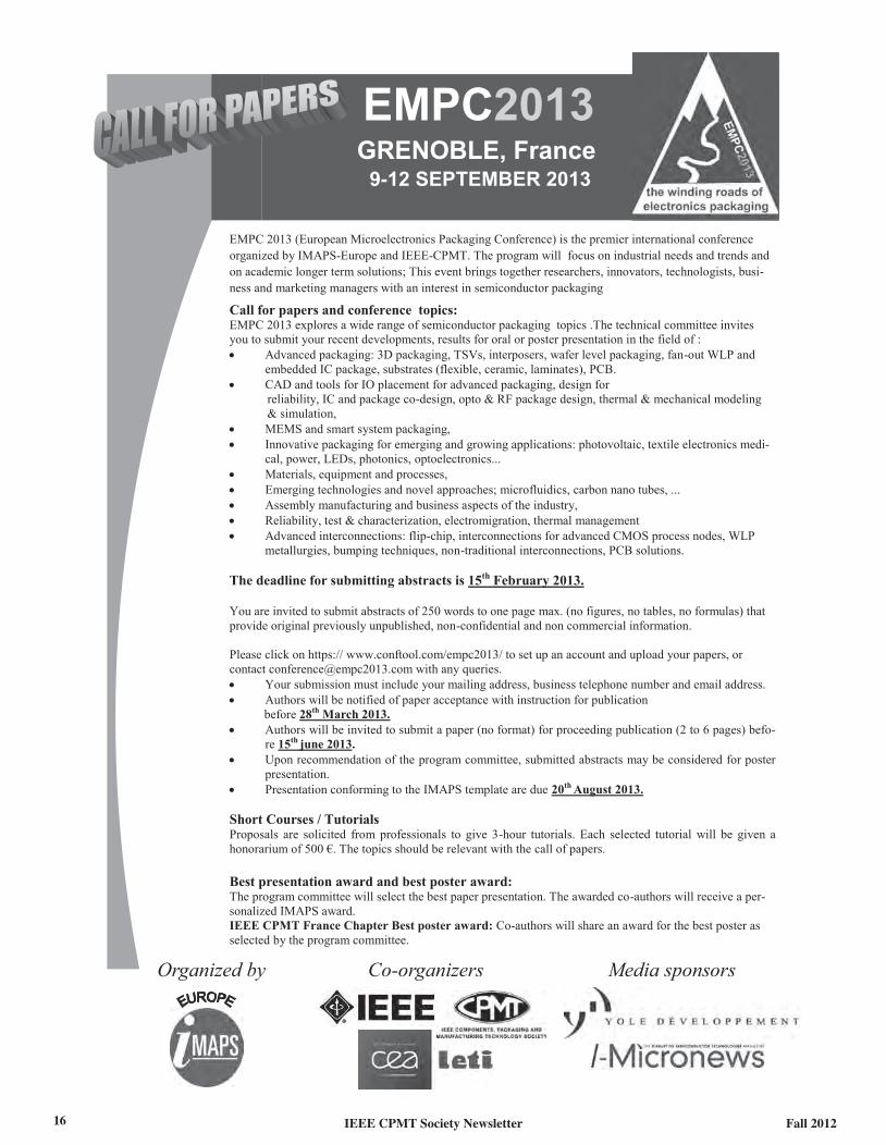
EMPC2013
GRENOBLE, France 9-12 SEPTEMBER 2013
EMPC 2013 (European Microelectronics Packaging Conference) is the premier international conference organized by IMAPS-Europe and IEEE-CPMT. The program will focus on industrial needs and trends and on academic longer term solutions; This event brings together researchers, innovators, technologists, busi-ness and marketing managers with an interest in semiconductor packaging
Call for papers and conference topics: EMPC 2013 explores a wide range of semiconductor packaging topics .The technical committee invites you to submit your recent developments, results for oral or poster presentation in the field of :
Advanced packaging: 3D packaging, TSVs, interposers, wafer level packaging, fan-out WLP and embedded IC package, substrates (flexible, ceramic, laminates), PCB. CAD and tools for IO placement for advanced packaging, design for
reliability, IC and package co-design, opto & RF package design, thermal & mechanical modeling & simulation,
MEMS and smart system packaging, Innovative packaging for emerging and growing applications: photovoltaic, textile electronics medi-cal, power, LEDs, photonics, optoelectronics... Materials, equipment and processes, Emerging technologies and novel approaches; microfluidics, carbon nano tubes, ... Assembly manufacturing and business aspects of the industry, Reliability, test & characterization, electromigration, thermal management Advanced interconnections: flip-chip, interconnections for advanced CMOS process nodes, WLP metallurgies, bumping techniques, non-traditional interconnections, PCB solutions.
The deadline for submitting abstracts is 15th February 2013. You are invited to submit abstracts of 250 words to one page max. (no figures, no tables, no formulas) that provide original previously unpublished, non-confidential and non commercial information. Please click on https:// www.conftool.com/empc2013/ to set up an account and upload your papers, or contact [email protected] with any queries.
Your submission must include your mailing address, business telephone number and email address. Authors will be notified of paper acceptance with instruction for publication
before 28th March 2013. Authors will be invited to submit a paper (no format) for proceeding publication (2 to 6 pages) befo-re 15th june 2013. Upon recommendation of the program committee, submitted abstracts may be considered for poster presentation. Presentation conforming to the IMAPS template are due 20th August 2013.
Short Courses / Tutorials Proposals are solicited from professionals to give 3-hour tutorials. Each selected tutorial will be given a honorarium of 500 €. The topics should be relevant with the call of papers. Best presentation award and best poster award: The program committee will select the best paper presentation. The awarded co-authors will receive a per-sonalized IMAPS award. IEEE CPMT France Chapter Best poster award: Co-authors will share an award for the best poster as selected by the program committee.
Organized by Co-organizers Media sponsors
17Fall 2012 IEEE CPMT Society Newsletter
CALL FOR PAPERS
15th IEEE International Symposium and Exhibition on
Advanced Packaging Materials
Time: February 27 to March 1, 2013
Location: Atrium Hotel, Irvine, California, USA Sponsor: IEEE Components, Packaging and Manufacturing Technology (CPMT) Society
Abstracts are solicited in the following topical areas: Adhesives and underfills - materials & applications, advanced processes, and reliability Circuit boards, substrates, and dielectrics - advanced circuit boards and substrates, properties, and processing Encapsulants, thin films, and coatings - materials & applications, new processes, and reliability Flip-chip interconnect materials and processing - bumping materials, bumping methods, and reliability evaluations Manufacturing and Reliability - New manufacturing techniques and testing Materials and processes for 3-D integration - thru-silicon-via formation, stacking, plating and bonding Optoelectronic and microwave materials - New materials and processes for optoelectronic and microwave packaging Solders and soldering operations - lead-free solders, new bonding and soldering processes, reliability Posters
Who should attend: Attendees of this symposium have been researchers, developers, producers and users of materials and processes for packaging the whole range of electronic and optoelectronic products.
Abstract submission: For presenting a paper in this symposium, please send an abstract (~ 150 words) via e-mail to [email protected] and copy [email protected]. Please include your affiliation, mailing address, phone number, and e-mail address in your submission.
Important dates: Abstract submission deadline: December 15, 2012. Acceptance notice: within 4 weeks of abstract receipt or Dec 31, 2012, whichever is earlier. Full manuscript submission deadline: January 15, 2013
For more information, please contact: General Chair: Tom Gregorich, Broadcom, Irvine, California, [email protected] Program Chair: Chin C. Lee, University of California, Irvine, California, [email protected] Publicity Chair: Sam Karikalan, Broadcom, Irvine, California, [email protected]
18 IEEE CPMT Society Newsletter Fall 2012

19Fall 2012 IEEE CPMT Society Newsletter
20 IEEE CPMT Society Newsletter Fall 2012

21Fall 2012 IEEE CPMT Society Newsletter

22 IEEE CPMT Society Newsletter Fall 2012
Name: 2012 IEEE 14th Electronics Packaging Technology
Conference - (EPTC)
Dates: December 5–7, 2012
Location: Singapore, Singapore
URL: http://www.eptc-ieee.net/index.html
Name: 2012 IEEE Electrical Design of Advanced Packaging
and Systems Symposium (EDAPS)
Dates: December 9–11, 2012
Location: Taipei, Taiwan
URL: http://edaps2012.ntu.edu.tw/
Name: 2012 IEEE CPMT Symposium Japan (Formerly VLSI
Packaging Workshop of Japan)
Dates: December 10–12, 2012
Location: Kyoto, Japan
URL: http://www.vlsi-pkg-ws.org/
Name: 2012 14th International Conference on Electronic
Materials and Packaging (EMAP)
Dates: December 13–16, 2012
Location: Lantau Island, Hong Kong
URL: http://ihome.ust.hk/~emap2012//index.html
Name: 2013 IEEE 15th International Symposium and
Exhibition on Advanced Packaging Materials
(APM)
Abstract Submission Date: December 15, 2012
Dates: February 27–March 1, 2013
Location: Irvine, CA USA
URL: http://www.apm2013.org/
Name: 2013 14th International Symposium on Quality
Electronic Design (ISQED)
Dates: March 4–6, 2013
Location: Santa Clara, CA, USA
URL: http://www.isqed.org/
Name: 2013 IEEE/CPMT 29th Semiconductor Thermal
Measurement & Management Symposium
(SEMI-THERM)
Dates: March 17–21, 2013
Location: San Jose, CA, USA
URL: http://www.semi-therm.org/
Name: 2013 14th Thermal, Mechanical and Multiphysics
Simulation and Experiments in Micro-Electronics and
Micro-Systems Conference (EuroSimE)
Dates: April 14–17, 2013
Location: Wroclaw, Poland
URL: http://www.eurosime.org/index.htm#
Name: 2013 Symposium on Design, Test, Integration and
Packaging of MEMS/MOEMS (DTIP)
Dates: April 16–18, 2013
Location: Barcelona, Spain
URL: http://cmp.imag.fr/conferences/dtip/dtip2013/index.php
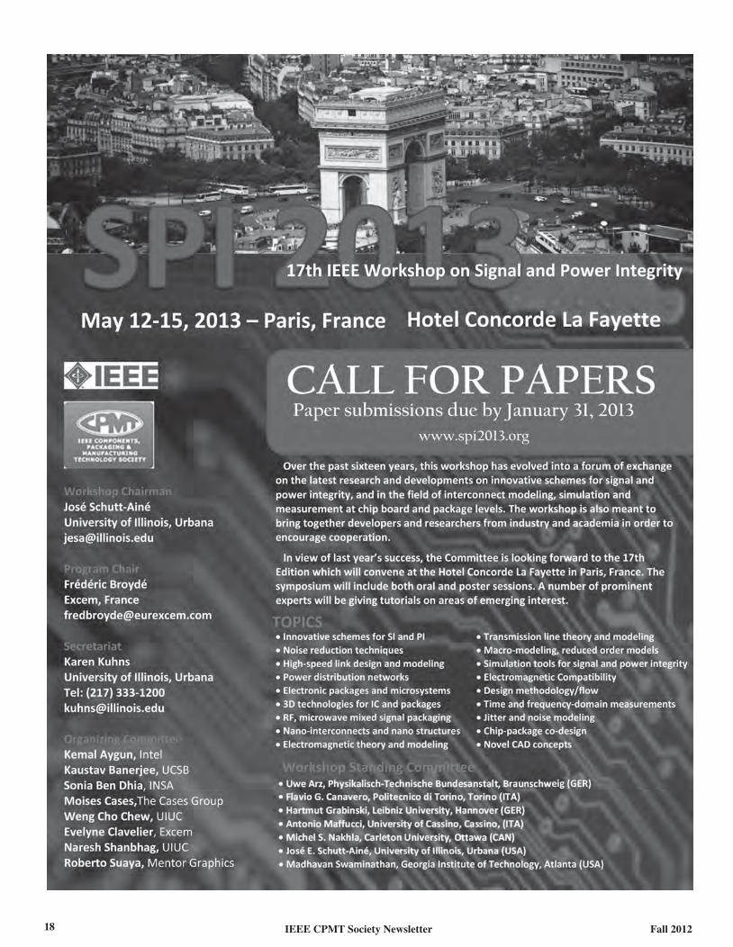
Name: 2013 17th IEEE Workshop on Signal and Power
Integrity (SPI)
Abstract Submission Date: January 31, 2013
Dates: May 12–15, 2013
Location: Paris, France
URL: http://spi2013.ece.illinois.edu/
Name: 2013 24th Annual SEMI Advanced Semiconductor
Manufacturing Conference (ASMC)
Dates: May 14–16, 2013
Location: Saratoga Springs, NY, USA
URL: http://www.semi.org/asmc2013
Name: 2013 IEEE 63rd Electronic Components and Technol-
ogy Conference (ECTC)
Dates: May 25–June 2, 2013
Location: Las Vegas, NV, USA
URL: http://www.ectc.net
Name: 2013 IEEE Semiconductor Wafer Test Workshop
(SWTW 2013)
Abstract Submission Date: February 22, 2013
Dates: June 8–12, 2013
Location: San Diego, CA, USA
URL: http://www.swtest.org/
Name: 2013 35th Annual Electrical Overstress/Electrostatic
Discharge Symposium (EOS/ESD)
Dates: September 8–13, 2013
Location: Las Vegas, NV, USA
URL: http://www.esda.org
Name: 2013 IMAPS-Europe European Microelectronics and
Packaging Conference (EMPC)
Dates: September 9–12, 2013
Location: Grenoble, France
URL: http://www.empc2013.com/
Name: 2013 IEEE 59th Holm Conference on Electrical Con-
tacts (Holm 2013)
Abstract Submission Date: January 20, 2013
Dates: September 22–25, 2013
Location: Newport, RI, USA
URL: http://www.ewh.ieee.org/soc/cpmt/tc1/h2013/
h2013call.html
Upcoming CPMT Society Sponsored and Cosponsored Conferences

23Fall 2012 IEEE CPMT Society Newsletter
Name: 2013 IEEE International 3D Systems Integration Con-
ference (3DIC)
Dates: October 2–4, 2013
Location: San Francisco, CA, USA
URL: http://www.3dic-conf.org/
Name: 2013 IEEE 22nd Conference on Electrical Perfor-
mance of Electronic Packaging and Systems (EPEPS)
Dates: October 27–30, 2013
Location: San Jose, CA, USA
URL: http://epeps.ece.illinois.edu/
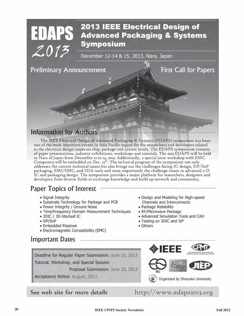
Name: 2013 IEEE Electrical Design of Advanced Packaging
& Systems Symposium (EDAPS)
Abstract Submission Date: June 25, 2013
Dates: December 12–14, 2013
Location: Nara, Japan
URL: http://www.edaps2013.org/
Name: 2014 IEEE 64th Electronic Components and Technol-
ogy Conference (ECTC)
Abstract Submission Date: October 15, 2013
Dates: May 23–31, 2014
Location: Orlando, FL, USA
URL: http://www.ectc.net
Name: 2014 IEEE Semiconductor Wafer Test Workshop
(SWTW 2014)
Abstract Submission Date: February 14, 2014
Dates: June 6–11, 2014
Location: San Diego, CA, USA
URL: http://www.swtest.org/
Name: 2014 5th Electronic System Integration Technology
Conference (ESTC)
Dates: September 15–18, 2014
Location: Helsinki, Finland
On the Web…..at cpmt.ieee.org
Content for CPMT Society Members only (click on Members Only tab)
IEEE/CPMT Workshop: “Thin Is In: Thin Chip & Packaging Technologies as Enabler for Innovative Mobile Devices”
(July 2012 at SEMICON West 2012)
Electronic products, such as smart phones, tablets and other consumer products drive the overall trend of maximum functional
integration in the smallest and thinnest package with lowest packaging costs. Here, thin 3D-packaging is one of the key Technolo-
gies to achieve these goals. Developments have lately been made with various embedding technologies, such as Fan out WLP and
embedded devices. Higher integration levels and lower profiles are also achieved with wafer-level processes at which most R&D is
concentrated in the commercialization of 2.5D IC´s (with silicon interposer) & 3D ICs, as well as coreless substrate. Furthermore,
there is tremendous pressure to decrease overall package height even with the additional dies stacking through innovation in wafer
thinning, TSV, and ultrathin interconnects.
In this workshop, leaders from key segments of the eco-system shared their perspectives and experiences on the readiness for com-
mercialization and what the future directions and opportunities in this emerging area of “Thin Packaging Technology.
• Thin is In: Packaging for Mobile Applications, Steve Bezuk, Qualcomm CDMA Technologies
• The Thin Package Challenge Never Ends, Bernd Appelt, ASE Group
• ChipletTTM and ChipsetTTM: A Fine Line Multilayer Flex Based Embedded Die Semiconductor Packaging Solution, Ted Tessier, Flip Chip International LLC
• Coreless Substrate. Its Performance and Future Direction, Mitsuharu Shimizu, Shinko
• Amkor’s Thru Molded Via (TMV) Thin Package on Package Technology Roadmap, Robert Lanzone, Amkor Technology

24 IEEE CPMT Society Newsletter Fall 2012
IEEE Components, Packaging and ManufacturingTechnology SocietyMarsha Tickman, Executive Director445 Hoes LanePiscataway, NJ 08854 USA
Getting the Most out of IEEE and CPMT Membership: eBooks
Did you know that IEEE members now have access to more than 220 eBooks from the IEEE Press collection
through IEEE Xplore, including: handbooks; introductory and advanced texts; reference works; professional books.
Follow 3 simple steps:1. Log in to IEEE Xplore http://www.ieeexplore.ieee.org/Xplore/guesthome.jsp using your IEEE Member Web
account.
2. Under the “Browse” heading in the left-hand navigation, click on “Books”.
3. Select the “Classics” tab from the top of the page. Under this tab you will find a listing of all the Free titles.
Here are a few examples of available books in pdf format: (more added every year)
1. Lead-Free Electronics: iNEMI Projects Lead to Successful Manufacturing by E. Bradley, C. Handwerker, J.
Bath, R. Parker and R. Gedney; Publication Date: 2007
2. Magnetic Actuators and Sensors by J. Brauer; Publication Date: 2006
3. Multigrid Finite Element Methods for Electromagnetic Field Modeling by Y. Zhu and A. Cangellaris; Publication
Date: 2006
4. Silicon Germanium: Technology, Modeling, and Design by R. Singh, H. Oprysko and D. Harame; Publication
Date: 2004
5. Integrated Passive Component Technology by R. Ulrich and L. Schaper; Publication Date: 2010
For more information visit: http://www.ieee.org/membership_services/membership/products/ebookclassics.html