controlled chlorine plasma reaction for noninvasive …dailab.stanford.edu/reprint/200. controlled...
TRANSCRIPT

Published: November 14, 2011
r 2011 American Chemical Society 19668 dx.doi.org/10.1021/ja2091068 | J. Am. Chem. Soc. 2011, 133, 19668–19671
COMMUNICATION
pubs.acs.org/JACS
Controlled Chlorine Plasma Reaction for NoninvasiveGraphene DopingJustin Wu,†,§ Liming Xie,†,§ Yanguang Li,† Hailiang Wang,† Yijian Ouyang,‡ Jing Guo,‡ and Hongjie Dai*,†
†Department of Chemistry, Stanford University, Stanford, California 94305, United States‡Department of Electrical and Computer Engineering, University of Florida, Gainesville, Florida 32611, United States
bS Supporting Information
ABSTRACT:We investigated the chlorine plasma reactionwith graphene and graphene nanoribbons and compared itwith the hydrogen and fluorine plasma reactions. Unlike therapid destruction of graphene by hydrogen and fluorineplasmas, much slower reaction kinetics between the chlorineplasma and graphene were observed, allowing for controlledchlorination. Electrical measurements on graphene sheets,graphene nanoribbons, and large graphene films grown bychemical vapor deposition showed p-type doping accom-panied by a conductance increase, suggesting nondestruc-tive doping via chlorination. Ab initio simulations wereperformed to rationalize the differences in fluorine, hydro-gen, and chlorine functionalization of graphene.
To realize the full potential of graphene, an interesting two-dimensional carbon material, various approaches have been
used to alter its structures through chemical modification inorder to achieve new properties such as band-gap engineeringor doping. Chemical functionalization of graphene, whether byhydrogen,1 fluorine,2,3 chlorine,4 or organic groups5 is one of theseapproaches. Different approaches and functionalizations haveshownmyriad outcomes ranging from graphene p-type6 or n-type7,8
doping, widening of its band gap to that of an insulator,2,4 orpassivation of edge structures.9
In this work, we focused on plasma reactions for graphenechemical modification. We investigated the chlorine plasmareaction with graphene and compared it with the results obtainedusing fluorine and hydrogen plasmas. Previous works usingseveral functionalization methods, including high-temperatureF2 exposure and hydrogen plasma,2�4,9 have shown extensivechanges and destruction as a result of covalent reactions withgraphene. Exposing graphene to a XeF2 atmosphere has beenfound to turn graphene into fluorographene, an insulating mate-rial with a band gap of 2.9 eV.2 Similarly, chlorination via a photo-chemical process altered graphene into an insulator.4 Graphane,the product of covalent bonding of hydrogen to graphene, is alsohighly insulating. All of these functionalizations by Cl, F, andH athigh coverage have been shown to destroy the network of gra-phene, rendering the material insulating.1
Here we carried out Cl, F, and H plasma reactions with gra-phene and graphene nanoribbons (GNRs). Raman spectroscopyfound that the chlorine plasma reaction with graphene exhibitedthe slowest kinetics, with the slowest increase of disorder over
reaction time (in minutes). In contrast, defects and disorder dur-ing plasma fluorination and hydrogenation of graphene increasedmuch more rapidly under short plasma exposures (in seconds).Raman and electrical transport measurements revealed p-dopingof graphene upon chlorination. Contrary to fluorine and hydro-gen plasma-reacted graphene devices, which rapidly decreased inconductance and became insulating, the conductance of Clplasma-treated graphene sheets and GNRs could be significantlyincreased as a result of p-doping without introducing extensivestructural damage. The results suggest a novel approach for ob-taining transparent graphene films with enhanced conductivity.
Pristine graphene sheets were prepared on SiO2/Si substrates(oxide thickness of 300 nm) by mechanical exfoliation.10 Single-and few-layer graphene sheets were identified by optical micro-scopy and confirmed by Raman spectroscopy.11 The graphenesamples were calcined at 400 �C to remove possible residuesbefore plasma treatment. Micro-Raman spectroscopic mappingsof the same graphene sheets were made before and after plasmatreatment using a Horiba HR800 Raman system with 532 nmexcitation. The plasma treatments were done in an electroncyclotron resonance (ECR) plasma etcher (Astex Plasmaquestmodel 357) at an ECR power of 200 W and a radiofrequencypower of 2 W with 10 mTorr Cl2, CF4, or H2 at room tem-perature. The power and pressure were held constant over thethree plasmas attempted.
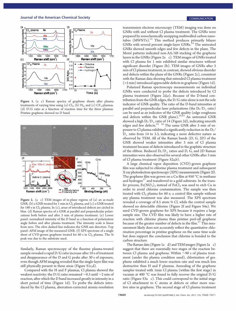
Figure 1a�c shows representative Raman spectra of single-layer graphene treated with Cl2 plasma, CF4 plasma, and H2
plasma, respectively. For Cl plasma-treated graphene, the gra-phitic G band was up-shifted by ∼3 cm�1 after 30 and 90 s oftreatment (Figure 1a), indicating possible p-type doping.12 TheD/G ratio increased only from 0 to 0.3 within 90 s of treatment,indicating that relatively mild disorder and defects (e.g., chlo-rinated sp3 carbon sites) were introduced by 90 s of Cl plasmatreatment. After 120 s of Cl plasma treatment, the D/G ratiojumped to >2 (Figure 1a,d), indicating that significantly moredisorder and defects were generated. On the other hand, H2
plasma and CF4 plasma treatments on graphene showed verydifferent results. The most rapid change in D/G ratio of the threeplasmas occurred with exposure to hydrogen plasma. A short 10 sexposure of graphene to H2 plasma led to a D/G ratio of ∼3.2.After 30 s of H2 plasma treatment, no Raman spectrum wasdetected, and atomic force microscopy (AFM) imaging revealedthat the single-layer regions of graphene had been completelyetched [see Figure S1a,b in the Supporting Information (SI)].
Received: September 27, 2011
19669 dx.doi.org/10.1021/ja2091068 |J. Am. Chem. Soc. 2011, 133, 19668–19671
Journal of the American Chemical Society COMMUNICATION
Similarly, Raman spectroscopy of the fluorine plasma-treatedsample revealed a rapid D/G ratio increase after 10 s of treatmentand disappearance of the D and G peaks after 30 s of exposure,even though AFM imaging revealed that the single-layer film wasstill physically present in these areas (Figure S1c,d).
Compared with the H and F plasmas, Cl plasma showed theweakest reactivity: the D/G ratio remained∼0.3 until∼2 min ofreaction, after which the D band increased greatly in intensity in ashort period of time (Figure 1d). To probe the defects intro-duced by the Cl plasma, aberration-corrected atomic-resolution
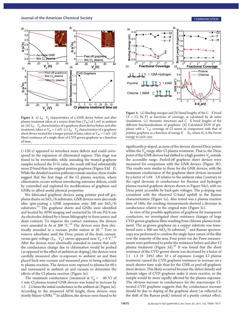
transmission electron microscopy (TEM) imaging was done onGNRs with and without Cl plasma treatment. The GNRs wereprepared by sonochemically unzipping multiwalled carbon nano-tubes (MWNTs).13 This method produces primarily bilayerGNRs with several percent single-layer GNRs.14 The untreatedGNRs showed smooth edges and few defects in the plane. TheMoir�e patterns indicated non-AA/AB stacking of the graphenelayers in the GNRs (Figure 2a�c). TEM images of GNRs treatedwith Cl plasma for 1 min exhibited similar structures withoutsignificant disorder (Figure 2b). TEM images of GNRs after 3min of Cl plasma treatment, in contrast, showed obvious disorderand defects within the plane of the GNRs (Figure 2c), consistentwith the Raman data showing that extended Cl plasma treatment(>2min) introduced appreciable defects in graphene (Figure 1d).
Polarized Raman spectroscopy measurements on individualGNRs were conducted to probe the defects introduced by Clplasma treatment (Figure 2d,e). Because of the D-band con-tribution from theGNR edges, the D/G ratio alone is not the soleindicator of GNR quality. The ratio of the D-band intensities atparallel and perpendicular laser polarizations (the D )/D^ ratio)can be used as an indicator of the GNR quality (edge roughnessand defects within the GNR plane).14,15 An untreated GNRshowed a high D )/D^ ratio of 14 (Figure 2d), indicating smoothedges and few defects.14�16 The same GNR after 3 min of ex-posure to Cl plasma exhibited a significantly reduction in the D )/D^ ratio from 14 to 3.3, indicating a more defective nature asobserved by TEM. All of the Raman bands (D, G, 2D) of theGNR showed weaker intensities after 3 min of Cl plasmatreatment because of defects introduced to the graphitic structureof the ribbon. Reduced D )/D^ ratios and D, G, and 2D Ramanintensities were also observed for several other GNRs after 3 minof Cl plasma treatment (Figure S2a,b).
A large chemical vapor deposition (CVD)-grown graphenefilm was subjected to chlorine plasma treatment and subsequentX-ray photoelectron spectroscopy (XPS)measurements (Figure 2f).The graphene film was grown on a Cu film at 950 �C in methaneand hydrogen17 and transferred to a gold substrate. In the trans-fer process, Fe(NO3)3 instead of FeCl3 was used to etch Cu inorder to avoid chlorine contamination. The sample was thentreated with Cl2 plasma for 60 s; a control film sample withoutany plasma treatment was also measured. The XPS spectrumrevealed a coverage of 8.5 atom % Cl, while the control sampleshowed no detectable chlorine (Figure 2f and Figure S4a). Weused CVD-grown graphene for XPS because it requires a largesample size. The CVD film was likely to have a higher rate ofreaction with chlorine plasma than pristine peel-off graphenebecause of the greater number of defects in the film.17 This mea-surement likely does not accurately reflect the quantitative chlo-rination percentage in pristine graphene on the same time scalebut does support the conclusion that chlorine is bonded to thecarbon structure.
TheRamandata (Figure 1a�d) andTEM images (Figure 2a�c)suggest that there are essentially two stages of the reaction be-tween Cl plasma and graphene. Within ∼90 s of plasma treat-ment (under the plasma condition used), chlorination of gra-phene exhibited a much lower reaction rate and was much lessdestructive than H and F plasmas. Annealing of the graphenesamples treated with 1min Cl plasma (within the first stage) invacuum at 400 �C was found to fully recover the original D/Gratio (Figure S3a�c). This could correspond to the initial stageof Cl attachment to C atoms at defects or other more reac-tive sites in graphene. The second stage of Cl plasma treatment
Figure 2. (a�c) TEM images of in-plane regions of (a) an as-madeGNR, (b) a GNR treated for 1 min in Cl2 plasma, and (c) a GNR treatedfor 180 s in Cl2 plasma. In (c), areas of introduced defects are circled inblue. (d) Raman spectra of a GNR at parallel and perpendicular polari-zations both before and after 3 min of plasma treatment. (e) Lowerpanel: normalized intensity of the D band as a function of polarizationangle before and after plasma treatment. The intensity scale is linearfrom zero. The olive dashed line indicates the GNR axis direction. Toppanel: AFM image of the measured GNR. (f) XPS spectrum of a singlesheet of CVD-grown graphene treated for 60 s in Cl2 plasma. The Sipeak was due to the substrate used.
Figure 1. (a�c) Raman spectra of graphene sheets after plasmatreatments of varying time using (a) Cl2, (b) H2, and (c) CF4 plasmas.(d) D/G ratio as a function of reaction time for the three plasmas.Pristine graphene showed no D band.
19670 dx.doi.org/10.1021/ja2091068 |J. Am. Chem. Soc. 2011, 133, 19668–19671
Journal of the American Chemical Society COMMUNICATION
(>120 s) appeared to introduce more defects and could corre-spond to the expansion of chlorinated regions. This stage wasfound to be irreversible; while annealing the treated graphenesamples reduced the D/G ratio, the result still had substantiallymore D band than the original pristine graphene (Figure S3d�f).While the detailed reaction pathways remain unclear, these resultssuggest that the first stage of the Cl plasma reaction, wherechlorination occurs without introducing extensive defects, couldbe controlled and exploited for modifications of graphene andGNRs to afford useful physical properties.
We fabricated graphene devices using pristine peel-off gra-phene sheets on SiO2/Si substrates. GNRdevices were alsomadeafter spin-coating a GNR suspension onto 300 nm SiO2/Sisubstrates.13 The graphene sheets and GNRs were identifiedand located by AFM imaging and contacted by 18 nm Pd/4 nmAu electrodes defined by e-beam lithography to form source anddrain contacts. To improve the contact resistance, the deviceswere annealed in Ar at 200 �C.18 The devices were then elec-trically annealed in a vacuum probe station at 10�6 Torr toremove adsorbates until the Dirac points of the drain current-versus-gate voltage (Ids�Vg) curves appeared near Vg = 0 V.7,19
After the devices were electrically annealed to ensure that onlythe conductance change due to chlorination would be probed(as opposed to the effect of ambient air doping), the devices werecarefully measured after re-exposure to ambient air and thenplaced back into vacuum and measured prior to being subjectedto plasma reaction. The devices were exposed to plasma for 60 sand remeasured in ambient air and vacuum to determine theeffects of the Cl plasma reaction (Figure 3a).
The maximum conductance (measured at Vg = �40 V) of1 min Cl plasma-treated GNR devices was found to increase by1.3�2.2 times the initial conductance in the ambient air (Figure 3a).According to the measured AFM height, these devices weremostly bilayer GNRs.14 In addition, the devices were found to be
significantly p-doped, as none of the devices showed Dirac pointswithin the Vg range after Cl plasma treatment. That is, the Diracpoint of the GNRdevices had shifted to a high positiveVg outsidethe accessible range. Peeled-off graphene sheet devices weremeasured for comparison with the GNR devices (Figure 3b).The results were similar to those for the GNR devices, with themaximum conductance of the graphene sheet devices increasedby a factor of 1.04�1.8 relative to the ambient value (contrary tothe rapid decrease in conductance for fluorine and hydrogenplasma-reacted graphene devices shown in Figure S4a), with noDirac point accessible by back-gate voltages. The p-doping wasconsistent with the observed G-band upshift in the Ramancharacterization (Figure 1a). Also tested was a plasma reactiontime of 180s; the resulting measurements showed a decrease inconductance relative to the original state (Figure 3c).
In view of the possible application of graphene for transparentconductors, we investigated sheet resistance changes of largeCVD-grown graphene films resulting from chlorine plasma treat-ment. The as-grown graphene on a copper substrate was trans-ferred onto a 300 nm SiO2/Si substrate,
17 and Raman spectros-copy was performed to confirm the single-layer nature of the filmover the majority of the area. Four-point van der Pauw measure-ments were performed to probe the resistance before and after Clplasma treatment (Figure 3d).20 It was found that the sheetresistance of the CVD-grown sheets was decreased by a factor of1.1�1.3 (8�24%) after 10 s of exposure. Longer Cl plasmatreatment caused the CVD graphene resistance to increase on amuch shorter time scale than for the GNR or peel-off graphenesheet devices. This likely occurred because the defect density anddomain edges of CVD graphene make it more reactive, so thesample would be more rapidly affected by the plasma exposure.The obvious increase in conductance for the macroscopic Cl-treated CVD graphene suggests that the conductance increaseshould be due to doping of the graphene sheet (as reflected inthe shift of the Raman peak) instead of a purely contact effect.
Figure 3. a) Ids�Vg characteristics of a GNR device before and afterplasma treatment taken at a source drain bias (Vds) of 1 mV in ambientair. (b) Ids�Vg characteristics of a graphene sheet device before and aftertreatment, taken at Vds = 1 mV. (c) Ids�Vg characteristics of a graphenesheet device treated for a longer period of time, taken at Vds = 1 mV. (d)Sheet resistance of a single sheet of CVD-grown graphene as a functionof time.
Figure 4. (a) Binding energies and (b) bond lengths of the C�X bond(X = Cl, H, F) as functions of coverage, as calculated by ab initiosimulations. (c) Atomistic structures and C�X bond lengths of thedifferent functionalizations of graphene. (d) Calculated DOS of gra-phene with a 1/30 coverage of Cl atoms in comparison with that ofpristine graphene as a function of energy E� EF, where EF is the Fermienergy in each case.

19671 dx.doi.org/10.1021/ja2091068 |J. Am. Chem. Soc. 2011, 133, 19668–19671
Journal of the American Chemical Society COMMUNICATION
Taken together, the electrical data reveal enhanced electricalconductance of peel-off graphene, GNRs, and CVD-grown gra-phene films resulting from controlled chlorination.
To rationalize the effects of plasma treatment on graphene,ab initio simulations (see the SI for details) were performed forCl, F, and H binding with one side of graphene (as our graphenewas deposited on substrates with the bottom side protected) inorder to gauge the relative reactivity of each of the plasma species.Both the bond lengths and bond energies were calculated as afunction of the fractional coverage (Figure 4a,b). Regardless ofthe coverage of sp3 species, we found that the chlorine bond tographene showed significantly lower binding energy and longerbond length (Figure 4c) than bonds to fluorine or hydrogen. Thefact that the simulated chlorine binding energy is significantlysmaller than that of hydrogen and fluorine suggests that thereaction is energetically less favorable (Figure 4a), which isconsistent with the observation of the low chlorination rate inFigure 1a. In regard to the reactions of hydrogen versus fluorineplasmas, while the calculations suggested that the thermody-namics of the hydrogen reaction is less energetically favorablethan the fluorine reaction, the Raman data indicated that thereaction occurs more rapidly. The hydrogen reaction appears toetch the graphene rapidly (Figure S1a,b), as opposed to fluorina-tion, through which the modeled fluorinated structure is the finalproduct. Thus, the energetics from simulations may not fullyreflect the entire reaction. It should also be noted that theconnection between the binding energy and the reaction rate isonly qualitative and can be complicated by sp3 hybridization andetching defects. Figure 4d compares the calculated density ofstates (DOS) of pristine graphene and chlorinated graphene at1/30 coverage. After chlorination, the DOS D(E) increases in theenergy range E < 0, and the Dirac point [the energy at whichD(E) ≈ 0] is ∼0.6 eV above the Fermi energy (EF), indicatingp-type doping. Furthermore, Mulliken charge analysis showedthat an electron charge of ∼0.2 is transferred from graphene toeach chlorine atom.
In summary, we have investigated the reactions of chlorine,hydrogen, and fluorine plasmas with several types of graphenematerials and found that chlorine plasma is the weakest and mostcontrollable for graphene doping. This is consistent with theweaker binding energy between Cl and graphene as determinedby ab initio calculations. Further investigation of chlorine plasmaeffects on graphene suggests that the length of exposure results intwo stages: in the first stage, chlorination occurs fairly nondes-tructively and reversibly; in the second, at longer exposure times,larger-area defects begin to form irreversibly. In the shorter timeframe, XPS directly showed the presence of chlorine. Exfoliatedgraphene and GNR devices showed p-type doping, and four-pointmeasurements onCVD-grown graphene showed an increasein conductance.
’ASSOCIATED CONTENT
bS Supporting Information. Experimental procedures,GNR and CVD growth of graphene, TEM and Raman char-acterization, device fabrication, details regarding the bindingenergy calculations, AFM images after hydrogen or fluorineplasma treatment, additional Raman spectra of GNRs, Ramanspectra showing the reversibility of chlorination, XPS of thecontrol sample, and conductivity measurements on a fluori-nated device. This material is available free of charge via theInternet at http://pubs.acs.org.
’AUTHOR INFORMATION
Corresponding [email protected]
Author Contributions§These authors contributed equally.
’ACKNOWLEDGMENT
This work was supported by MARCO MSD, Intel, ONRMURI on graphene, and Samsung Electronics. The work at UFwas supported by ONR and NSF. TEMwas done at the NationalCenter for Electron Microscopy at Lawrence Berkeley NationalLaboratory, which is supported by the U.S. Department ofEnergy under Contract DE-AC02-05CH11231.
’REFERENCES
(1) Elias, D. C.; Nair, R. R.; Mohiuddin, T. M. G.; Morozov, S. V.;Blake, P.; Halsall, M. P.; Ferrari, A. C.; Boukhvalov, D. W.; Katsnelson,M. I.; Geim, A. K.; Novoselov, K. S. Science 2009, 323, 610.
(2) Robinson, J. T.; Burgess, J. S.; Junkermeier, C. E.; Badescu, S. C.;Reinecke, T. L.; Perkins, F. K.; Zalalutdniov, M. K.; Baldwin, J. W.;Culbertson, J. C.; Sheehan, P. E.; Snow, E. S. Nano Lett. 2010, 10, 3001.
(3) Withers, F.; Dubois, M.; Savchenko, A. K. Phys. Rev. B 2010,82, No. 073403.
(4) Li, B.; Zhou, L.; Wu, D.; Peng, H.; Yan, K.; Zhou, Y.; Liu, Z. ACSNano 2011, 5, 5957.
(5) Farmer, D. B.; Lin, Y.; Afzali-Ardakani, A.; Avouris, P. Appl. Phys.Lett. 2009, 94, No. 213106.
(6) Chen, W.; Chen, S.; Qi, D. C.; Gao, X. Y.; Wee, A. T. S. J. Am.Chem. Soc. 2007, 129, 10418.
(7) Wang, X.; Li, X.; Zhang, L.; Yoon, Y.; Weber, P. K.; Wang, H.;Guo, J.; Dai, H. Science 2009, 324, 768.
(8) Lin, Y.; Lin, C.; Chiu, P. Appl. Phys. Lett. 2010, 96, No. 133110.(9) Lu, Y. H.; Wu, R. Q.; Shen, L.; Yang, M.; Sha, Z. D.; Cai, Y. Q.;
He, P. M.; Feng, Y. P. Appl. Phys. Lett. 2009, 94, No. 122111.(10) Novoselov, K. S.; Geim, A. K.; Morozov, S. V.; Jiang, D.; Zhang,
Y.; Dubonos, S. V.; Grigorieva, I. V.; Firsov, A. A. Science 2004, 306, 666.(11) Malard, L. M.; Pimenta, M. A.; Dresselhaus, G.; Dresselhaus,
M. S. Phys. Rep. 2009, 473, 51.(12) Subrahmanyam, K. S.; Voggu, R.; Govindaraj, A.; Rao, C. N. R.
Chem. Phys. Lett. 2009, 472, 96.(13) Jiao, L.; Wang, X.; Diankov, G.; Wang, H.; Dai, H. Nat.
Nanotechnol. 2010, 5, 321.(14) Xie, L.; Wang, H.; Jin, C.; Wang, X.; Jiao, L.; Suenaga, K.; Dai,
H. J. Am. Chem. Soc. 2011, 133, 10394.(15) Casiraghi, C.; Hartschuh, A.; Qian, H.; Piscanec, S.; Georgi, C.;
Fasoli, A.; Novoselov, K. S.; Basko, D. M.; Ferrari, A. C.Nano Lett. 2009,9, 1433.
(16) Canc-ado, L. G.; Pimenta, M. A.; Neves, B. R. A.; Dantas,M. S. S.; Jorio, A. Phys. Rev. Lett. 2004, 93, No. 247401.
(17) Li, X.; Cai, W.; An, J.; Kim, S.; Nah, J.; Yang, D.; Piner, R.;Velamakanni, A.; Jung, I.; Tutuc, E.; Banerjee, S. K.; Colombo, L.; Ruoff,R. S. Science 2009, 324, 1312.
(18) Javey, A.; Guo, J.; Wang, Q.; Lundstrom, M.; Dai, H. Nature2003, 424, 654.
(19) Moser, J.; Barreiro, A.; Bachtold, A. Appl. Phys. Lett. 2007,91, No. 163513.
(20) Van der Pauw, L. J. Philips Res. Rep. 1958, 13, 1.