cost-effective high- applications
TRANSCRIPT

Integration Design of Chip and Package for
Cost-Effective High-Speed Applications
Nansen Chen, Hongchin Lin, Nan-Cheng Chen, Roger Wu, Tomson Chou, andHerbie Chien
Abstract - Low cost is the trend for consumerelectronics. However, the challenges of the LCD-TVprocessor using cost-effective two-layer ball gridarray (BGA) packages suffer from serious crosstalkand return loss due to lack of a solid plane to suppressthe coupling effect and control the trace impedance.Two types of two-layer BGA packages were measuredand simulated using a 3D full-wave electromagneticfield solver and an EM-based 3D parasitic extractorto analyze their speed limitations and power couplingbetween the signals and the power net. The resultsindicated the signal coupling is the dominant factorfor insertion loss. Thus, the design guidelines andspecifications using two-layer BGA packages areproposed for development of the next generationprocessors.
I. INTRODUCTION
Many reports have indicated the LCD TV is the fastestgrowing product in TFT LCD applications. The trend ofLCD TV includes the larger panel, higher resolution, andlower cost. In addition to the panel, the most importantcomponent in the LCD TV is the processor. The processordrives an external DDR SDRAM that is used for the textand graphic generations, or MPEG buffer. Therefore, thespeed of the memory interface influences the LCD-TVperformance. Most of LCD-TV processors wereencapsulated using the higher cost four-layer ball gridarray (BGA) packages to preserve the signal quality at thehigh-speed memory interface. However, the two-layerBGA package embedded with the plating lines may beconsidered for low cost requirement. In this paper, twotypes of two-layer packages were adopted and evaluated.A 3D full-wave electromagnetic field solver and an EM-based 3D parasitic extractor were used to analyze their S-parameters and power inductance for package design.Finally, the design guidelines and S-parametersspecifications of two-layer BAG package are suggestedfor the future product development.
Nansen Chen and Hongchin Lin are with the Departmentof Electrical Engineering, National Chung-Hsing University,Taichung, Taiwan, E-mail: nansen(a seed.net.tw,hclin(a:dragon.nchu.edu.tw; Nan-Cheng Chen, Roger Wu,Tomson Chou, and Herbie Chien are with MediaTek Inc.,Taiwan, E-mail: Charles Chen(a mtk.com.tw
IL. BGA PACKAGE LAYOUTS
The two kinds of two-layer BGA packages, AT02 andAT05, were used to encapsulate the LCD-TV processors.The detailed package parameters are given in Table I. Fig.1 shows parts of the high-speed signals and power/groundnet layouts including DQO-15, DQS0-4, DQMO, DVDD2(power net), and DVSS (ground net). The majordifference between the two layouts is two solder-ball rowsin AT05 and four solder-ball rows in AT02. The largertrace span is found in AT05 due to less ball rows. Sometraces in AT02 were designed in the form of serpentinethat servers as a delay line.
III. TESTING RESULTS AND SIMULATIONMETHODS
Both of the packages including the processor weretested on the PCB. The testing results indicated the speedlimitations for AT02 and AT05 are 378 Mbps and 332Mbp, respectively. However, the goal of data speed forAT02 is 400 Mbps, which is the maximum data speed ofDDR SDRAM. In the following sections, both of thepackage layouts are investigated using S-parametersimulations. Good trace layouts are preserved as reusablelayouts for the future package design.
For wideband digital signals, S-parameters contain theeffects of reflection or transmission of power for anynetwork [1]. Thus, S-parameters are useful to determinethe power scattering effect and power receivingperformance between signal ports, such as the couplingrelationship between the signals and the power net. A testload of 50 Q was used to measure the rising time (Tr,20%-80%) of 0.214 ns for the DQ signal at the loadterminal. The 3-dB bandwidth (F3dB) was calculated by0.35/Tr 1.6 GHz. Ansoft HFSS was utilized to extracttheir S-parameters up to 3 GHz based on the packagegeometry and material given in Table I. The extendedbandwidths are evaluated for higher speed, or smaller T,up to 125 ns. Both ends of gold wire and solder-ball forsignals or DVDD2 were assigned to lumped portsterminated to 50 Q. DVSS was connected to the idealground, which is 0.381 mm below the package.
0-7803-9339-2/05/$20.00 02005 IEEE. 621

IV. EVALUATION OF ELECTRICALCHARACTERISTICS
A. Signal Loss and Coupling effects
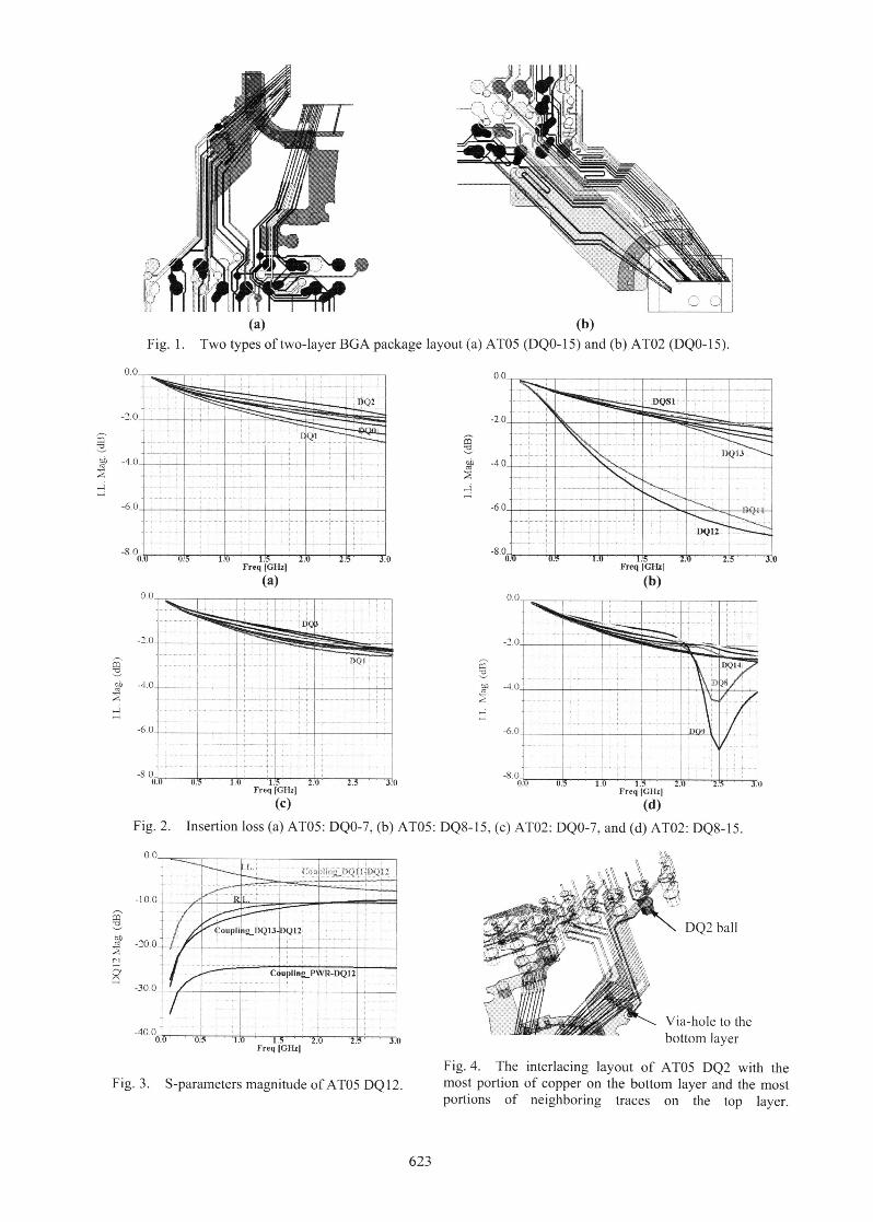
The drawback of two-layer BGA package is lack of asolid ground plane under the signal traces to control traceimpedance and suppress the crosstalk. Larger insertionloss will be expected because of larger return loss andcrosstalk. Fig. 2 shows the insertion losses for DQO-1 5 ofAT02 and AT05. From the rise time Tr measurementgiving the 3-dB frequency of 1.6 GHz, we can observethat for frequency lower than 1.6 GHz the insertion loss ofAT02 is less than that of AT05 due to the more seriousloss of DQ1 1 and DQ12 in AT05. Note that if these twotraces are failed, the chip can not work correctly. It is alsoworth noting that for DQ 8 and DQ9 on AT02, resonancemay be occurred at 2.5 GHz, which means the signalquality will be poor if their bit rates increase significantly.The largest insertion loss occurred at DQ12 in AT05 iscaused by the significant coupling between DQl 1 andDQ12 as shown in Fig. 3. Comparison of return loss andnear-end coupling for both packages is given in Fig. 5.The neighbor coupling in DQl 1-12 dominates theperformance in insertion loss, while return loss does not.Therefore, well control of signal coupling will be themajor challenge for high-speed signals using the two-layerBGA package. For example, the interlacing layout ofAT05 DQ2 illustrated in Fig. 4 gives the neighborcouplings less than -20dB, which is not shown in thispaper due to limitation of paper space.
B. Power Inductance and Coupling
Ansoft Maxwell 3-D Quick Parameter Extractor wasused to extract DVDD2 inductance. The simulatedinductance values are 1. l6nH and 3.20 nH for AT05 andAT02, respectively. Thus, the power net supplied to high-speed signals in both packages cannot be assumed as idealreference plane. The power inductance induces the powerdrop and simultaneous switching noise (SSN), calledpower noise. When the power noise occurs, the signaltraces will induce the noise coupling. Fig. 6 shows theDVDD2 coupling to the DQ lines. The power coupling isnot as serious as expected due to the thick BT core (0.4mm). Although the coupling magnitudes for frequencieslower than 1.6 GHz are insignificant, the trend of powercoupling is increasing when the data speed increases orthe data rise time decreases. If the non-ideal power netbeneath the high-speed traces is removed, the noisecoupling will be reduced.
V. LAYOUT GUIDELINES ANDSPECIFICATIONS
The goal to reuse the two-layer BGA packageembedded with the plating lines for the future LCD-TVprocessor is to ensure minimum insertion loss. To achievethis goal, well control of signal coupling or crosstalkbecomes the critical issue. Some suggestions for the two-layer substrate layout are as follows.
* Interlace the high-speed traces between the topand bottom layers.
* Reduce the length of parallel traces, including theplating line, which can reduce the crosstalksaturation [2].
* Insert the ground wire paralleled with the signaltrace, if possible, which can reduce the signalparasitic parameters and coupling effects.
* Move the signal as far away as possible from thepower net (DVDD2) on the same layer.
* For many high-speed I/Os on the package, usethree or four rows of I/O balls to reduce therouting span in the package.
* Carefully design the power nets, such as DVDD2,supplied to the high-speed signals to reduce theinductance. For instance, layout DVDD2 towardthe inner balls to shorten the electrical path.
* Avoid the high-speed I/O pads at the chip cornerthat can reduce the length of bondwire and tracerouting in the package.
Ref. [3] demonstrates another S-parameters analysisfor high-speed applications using the leadframe packages.With the analysis and the guidelines given above as wellas Ref. [3], the package specifications of signal loss andcoupling on DDR SDRAM interface could be defined inTable II. The smaller signal rise time is, the tighter lossbudget is.
VI. CONCLUSION
Lower cost two-layer BGA package could be achievedfor high-speed applications, such as the LCD-TVprocessors. This paper demonstrates the frequency domainanalysis of two types of two-layer BGA packages for thehigh-speed memory interface. Well control of signalcoupling is the major challenge when the two-layer BGApackage embedded with the plating lines is used. Thepackage design guidelines and specifications arepresented for the future product development. The futurework will be verification of the package specificationsfollowed by the guidelines.
REFERENCES
[1 ] T. C. Edwards and M. B. Steer, Foundations ofInterconnect and Microstrip Design, 3rd ed., New York:John Wiley & Sons, 2000, pp. 457-470.
[2] D.N. de Araujo, M. Cases, N. Pham, and E. Matoglu, "Co-design optimization of laminate substrates for high speedapplications," IEEE 54th Electronic Components andTechnology Conference, pp. 1776-1783, Jun. 2004.
[3] N. Chen and H. Lin, "Design and evaluation of chip onheat sink quad flat package (COHS-QFP) for consumerelectronics," iMAPS-Taiwan 2005 Technical Symposium,pp. 260-264, Jun. 2005.
622
(a) (b)Fig. 1. Two types of two-layer BGA package layout (a) AT05 (DQO-15) and (b) AT02 (DQO- 15).
0.0 ~~~~~~~~~~~~~~~~~~~~~~~~~~~~~~~~~~~~~~~~~~~~. . ...s.-... , . . . ...DQ2~~~~~~~~~~~~~~~~~~~~~~~~. ... .. . . .... ..... .-6 0 1 ----------------~~~~~~~~~~~~~~---------- ----------- ---------------
-4.0 0 11__3
Freq IGHzI(a)
0.0t ....
............
-4.0-6.............0...
8,0.0 0 15 1.10 125
Freq [GHz](c)
m
-4
20.. 225 3.10
(b)0.0-
-4 .0
..,
-6009
-8.....01 ............ ..... : ....n An I; ',Is Ifn 1. ;l.1.U 1. z >.'2U
Freq IGHzI(d)
Fig. 2. Insertion loss (a) AT05: DQO-7, (b) AT05: DQ8-15, (c) AT02: DQO-7, and (d) AT02: DQ8-15.
01o0 / CoupIi~jngDQ13-bQl2cliI(DI B ~ CupHing9PIVR-DQ12
0_
.0 '0|;o.5 '1. '1.5 2.0 2.5 1OFreq [GHzJ
Fig. 3. S-parameters magnitude of AT05 DQ12.
DQ2 ball
Via-hole to thebottom layer
Fig. 4. The interlacing layout of AT05 DQ2 with themost portion of copper on the bottom layer and the mostportions of neighboring traces on the top layer.
623
mct.b
4
..m
-T -
,. 1,: :. -. 1.
0
L
U.U U.Zl Z:!3 J
PQ3':

1-1)
m_/
0
.
o
0.0.
--2
.....7
-20.0T ______ ______
-30.0
°.~~~~~~~~~~~~~~~~~~~~~~~~~ ~~~~~~~~~~~~~ ;; 1. .l.2 .. ;2. ;. O
Freq [GHzl(c)
o.o
1-
01t4
01)1
2
Oil
zC._Q
uV4
Freq [GHz(b)
(d)Fig. 5. Return loss (a) AT05: DQ8-15, (b) AT02: DQO-7, and near-end coupling (c) AT05: DQ8-15, (d) AT02: DQO-7.
-10.0 .1-1 f- :.0
-4; : : .10-. -:-----:--
-50.0 D_1_2
Freq (GHzJ(a)
~g_s
I-C:
01)
Ml
0
;. _._..
-20.0- . pC
t * ~~~~~~~~~~-
-40.0_ .-4
''.'.-.-.'.'..'..''-. ...-'. .... -.'-..-"'' - ' ' ; .' -.'.'''.'.....-SC)~~~~~~~~~~~~~~~~.0 _ 1.1 2't ' 2 3Freq [GHzi
(b)Fig. 6. Power (DVDD2 balls) coupling to signal wires (a) AT02: DQ8-15 and (b) AT05: DQ8-15.
TABLE IDETAILED PACKAGE PARAMETERS
Code no. AT02 AT05Package size 27 x 27 x 2.2(LxWxH,mm)27x7x2.Ball count/pitch 388 / 1.0-mmTrace width/thickness 50127 um 1 55127 gmMold thickness 1.17 mm (Dk = 4.0, Df= 0.01)BT core thickness 0.4 mm (Dk 4.2, Df= 0.0 12)Solder-mask thickness 40 .9m(Dk 4.0 Df= 0.028)Gold-wire diameter 0.8 mil 0.9 milChip-pad pitch 60 gm 72 gmVia-hole diameter 0.2 mm
Metal conductivity (a) Copper: 5.8 x 10⁷/Q-mDVDD2 balls/wires 4/10 b 8/17
TABLE IIPACKAGE SPECIFICATIONS FOR SIGNAL LosS ANDCOUPLING
Item Max. SpecificationInsertion loss -3 dB|Average NE coupling -10 dBRetum loss -10 dBPower coupling -17 dB
624
-
011-
S.0
v1. -.1 .. .;.;. --.1
-10.0
-20.0
... -
j.-30.0
-40.0iaff- 0-115 1-wi 'I 5 -7111 7 A 7Vk
,J
T:
U.1J u.10 1. U Z.,: J.UISI