coupling dna nano-breadboards to solid state conductors
TRANSCRIPT
85EAI Energia, Ambiente e Innovazione 3/2015
Introduction
Recent advances in DNA nanotechnology have demonstrated the wide range of possibilities offered by the self-assembly of carefully programmed DNA sequences into functional nano-architectures (Box “DNA and DNA nanotechnology”). Two main approaches to the self-assemblage of DNA-based nano-architectures have been explored: one is based on the hierarchical assembly of “tiles” of different shapes and complexities into more complex structures via the use of suitably designed, protruding single strands (the so called “sticky ends”) [1,2]; this means building by basic bricks within a wide range of typologies [3-8]. A more recent approach is based on folding a long DNA single strand at selected locations by using short single strands to “staple” it in shape [9]; by analogy to the Japanese art of paper folding, this approach has been defined “DNA origami”. Indeed, this method has supplied the most attractive shapes at the nanometric scale, as demonstrated by countless
Atomic Force Microscopy (AFM) images of both bi- and three dimensional constructs with typical sizes of a few tens of nanometers. Figure 1 shows a limited collection of such architectural images. Uses of a hybrid tiles-origami approach were also envisaged [10].Beyond applications in nanomedicine, research is aiming at the applications of functional properties of DNA nanostructures in devices such as DNA nanoarrays for genomics and proteomics, nanosensor arrays for contaminants and toxins, and more generally in nanobioelectronics, where individual functional molecules must be addressed. Even if the power of DNA to create complex nano-sized shapes was largely demonstrated, very few works have dealt with the exploitation of such nano-architectures by organizing them in a useful order and establishing a technology
Coupling DNA nano-breadboards to solid state conductorsDNA is not only a most extraordinary information storage medium: the programmable pairing of DNA single strands into precisely engineered, connecting double helices make it an extremely appealing material for assemblage of nanoscale architectures. This is the basis of DNA nanotechnology, and designing almost any structure made of DNA at the nanometer scale, decorating it with a variety of functional molecules, and accomplishing it by virtually inexpensive self-assembly, is already a reality in many research laboratories in the world. But can we extend the range of applications of this technology by coupling DNA grafted molecular electronic nanocircuitry to solid state devices, and interface molecular smart functions to our senses? This challenging research is addressed by a collaborative research among ENEA, the Universities of Roma Tor Vergata and Aarhus, and the CNMS of the Oak Ridge National Laboratory. The first results obtained by our consortium pave the way to the technological ability to interface and use completely self-assembled, DNA-based electronic nano-breadboards, endowed with ultra-high-density functional organic components
DOI 10.12910/EAI2015-064
n L. Wang, C. Dalmastri, L. Mosiello, B. Rapone, S. Retterer, A. Krissanaprasit, K. Gothelf, P. Morales
Contact person: Piero [email protected]
Research & development
Research & development
86EAI Energia, Ambiente e Innovazione 3/2015
DNA and DNA nanotechnology
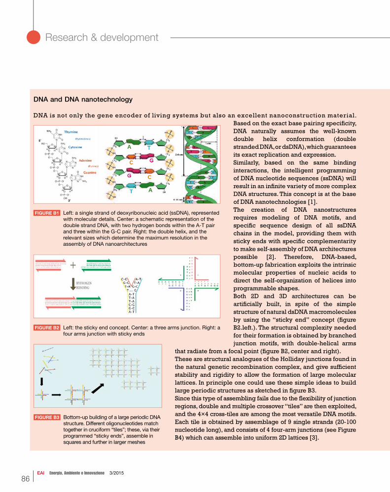
DNA is not only the gene encoder of living systems but also an excellent nanoconstruction material.Based on the exact base pairing specifi city, DNA naturally assumes the well-known double helix conformation (double stranded DNA, or dsDNA), which guarantees its exact replication and expression. Similarly, based on the same binding interactions, the intelligent programming of DNA nucleotide sequences (ssDNA) will result in an infi nite variety of more complex DNA structures. This concept is at the base of DNA nanotechnologies [1].The creation of DNA nanostructures requires modeling of DNA motifs, and specifi c sequence design of all ssDNA chains in the model, providing them with sticky ends with specifi c complementarity to make self-assembly of DNA architectures possible [2]. Therefore, DNA-based, bottom-up fabrication exploits the intrinsic molecular properties of nucleic acids to direct the self-organization of helices into programmable shapes.Both 2D and 3D architectures can be artifi cially built, in spite of the simple structure of natural dsDNA macromolecules by using the “sticky end” concept (fi gure B2.left.). The structural complexity needed for their formation is obtained by branched junction motifs, with double-helical arms
that radiate from a focal point (fi gure B2, center and right).These are structural analogues of the Holliday junctions found in the natural genetic recombination complex, and give suffi cient stability and rigidity to allow the formation of large molecular lattices. In principle one could use these simple ideas to build large periodic structures as sketched in fi gure B3.Since this type of assembling fails due to the fl exibility of junction regions, double and multiple crossover “tiles” are then exploited, and the 4×4 cross-tiles are among the most versatile DNA motifs. Each tile is obtained by assemblage of 9 single strands (20-100 nucleotide long), and consists of 4 four-arm junctions (see Figure B4) which can assemble into uniform 2D lattices [3].
FIGURE B1 Left: a single strand of deoxyribonucleic acid (ssDNA), represented with molecular details. Center: a schematic representation of the double strand DNA, with two hydrogen bonds within the A-T pair and three within the G-C pair. Right: the double helix, and the relevant sizes which determine the maximum resolution in the assembly of DNA nanoarchitectures
FIGURE B2 Left: the sticky end concept. Center: a three arms junction. Right: a four arms junction with sticky ends
FIGURE B3 Bottom-up building of a large periodic DNA structure. Different oligonucleotides match together in cruciform “tiles”; these, via their programmed “sticky ends”, assemble in squares and further in larger meshes
Res
earc
h &
dev
elop
men
t
87EAI Energia, Ambiente e Innovazione 3/2015
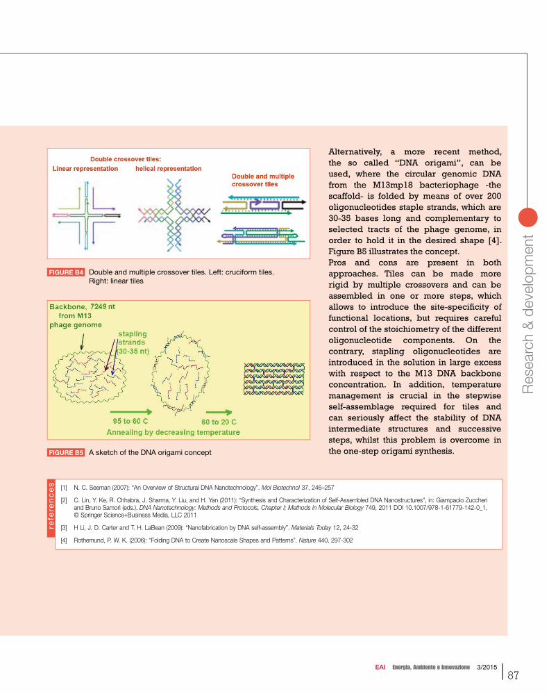
Alternatively, a more recent method, the so called “DNA origami”, can be used, where the circular genomic DNA from the M13mp18 bacteriophage -the scaffold- is folded by means of over 200 oligonucleotides staple strands, which are 30-35 bases long and complementary to selected tracts of the phage genome, in order to hold it in the desired shape [4]. Figure B5 illustrates the concept.Pros and cons are present in both approaches. Tiles can be made more rigid by multiple crossovers and can be assembled in one or more steps, which allows to introduce the site-specifi city of functional locations, but requires careful control of the stoichiometry of the different oligonucleotide components. On the contrary, stapling oligonucleotides are introduced in the solution in large excess with respect to the M13 DNA backbone concentration. In addition, temperature management is crucial in the stepwise self-assemblage required for tiles and can seriously affect the stability of DNA intermediate structures and successive steps, whilst this problem is overcome in the one-step origami synthesis.
FIGURE B4 Double and multiple crossover tiles. Left: cruciform tiles. Right: linear tiles
FIGURE B5 A sketch of the DNA origami concept
refe
ren
ce
s [1] N. C. Seeman (2007): “An Overview of Structural DNA Nanotechnology”. Mol Biotechnol 37, 246–257
[2] C. Lin, Y. Ke, R. Chhabra, J. Sharma, Y. Liu, and H. Yan (2011): “Synthesis and Characterization of Self-Assembled DNA Nanostructures”, in: Giampaolo Zuccheri and Bruno Samorì (eds.), DNA Nanotechnology: Methods and Protocols, Chapter I; Methods in Molecular Biology 749, 2011 DOI 10.1007/978-1-61779-142-0_1, © Springer Science+Business Media, LLC 2011
[3] H Li, J. D. Carter and T. H. LaBean (2009): “Nanofabrication by DNA self-assembly”. Materials Today 12, 24-32
[4] Rothemund, P. W. K. (2006): “Folding DNA to Create Nanoscale Shapes and Patterns”. Nature 440, 297-302
88EAI Energia, Ambiente e Innovazione 3/2015
to make them addressable and interfaced to solid-state, usable devices. A few attempts have aimed at organizing DNA origami on hydrophilic patterns on silicon oxide substrates [11]: the group of H. Yan produced an addressable network of DNA origami tubes bridging gold nanopillars (NPs) organized onto a silicon oxide substrate [12]; another important approach is due to Tuukkanen and colleagues [13], who immobilized individual DNA double strands between nanoelectrodes by driving them via dielectrophoresis. Our work aims at the possibility of using DNA nanostructures as “breadboards” for self-assembly of organic or biomolecular electronic components to be individually addressed. While recent important work has demonstrated the possibility of immobilizing individual protein molecules on selected locations within individual DNA nano-architectures [14-16], in order to complete the multiscale process we aim at organized immobilization of individual nano-architectures on electrically connected locations at the 10-100 nm scale. We have chosen the simplest DNA origami structures due to the high assemblage yield of DNA breadboards and to the possibility of endowing our breadboards with selective connecting pegs every 5-6 nm. These connecting structures are extensions of the “stapling”
DNA sequences that hold together the fl at breadboard; such extensions, if carefully programmed, are available for hybridization with a complementary sequence, such as a DNA aptameric sequence, or may be chemically conjugated to a protein component. Figure 2 shows the analogy between conventional electronic breadboards and our idea of a “DNA breadboard”.The high resolution with which individual functional organic molecules can be positioned on the breadboard, the fact that the breadboard itself is self-assembled in solution starting from selected DNA sequences, and can spontaneously anchor onto the gold connectors, and the ability of molecular components to self-assemble onto the breadboard (a virtually inexpensive process!) make the DNA nano-breadboards idea extremely appealing for the achievement of future molecular electronic devices. We are thus investigating the feasibility of the process by suspending DNA origami nano-breadboards across groups of four gold NPs, fabricated by electron beam lithography (EBL) at addressable coordinates on a silicon oxide substrate. This requires, on the one hand, the most advanced inorganic nanofabrication skills, in particular EBL, and on the other the ability to design DNA and DNA-protein architectures based
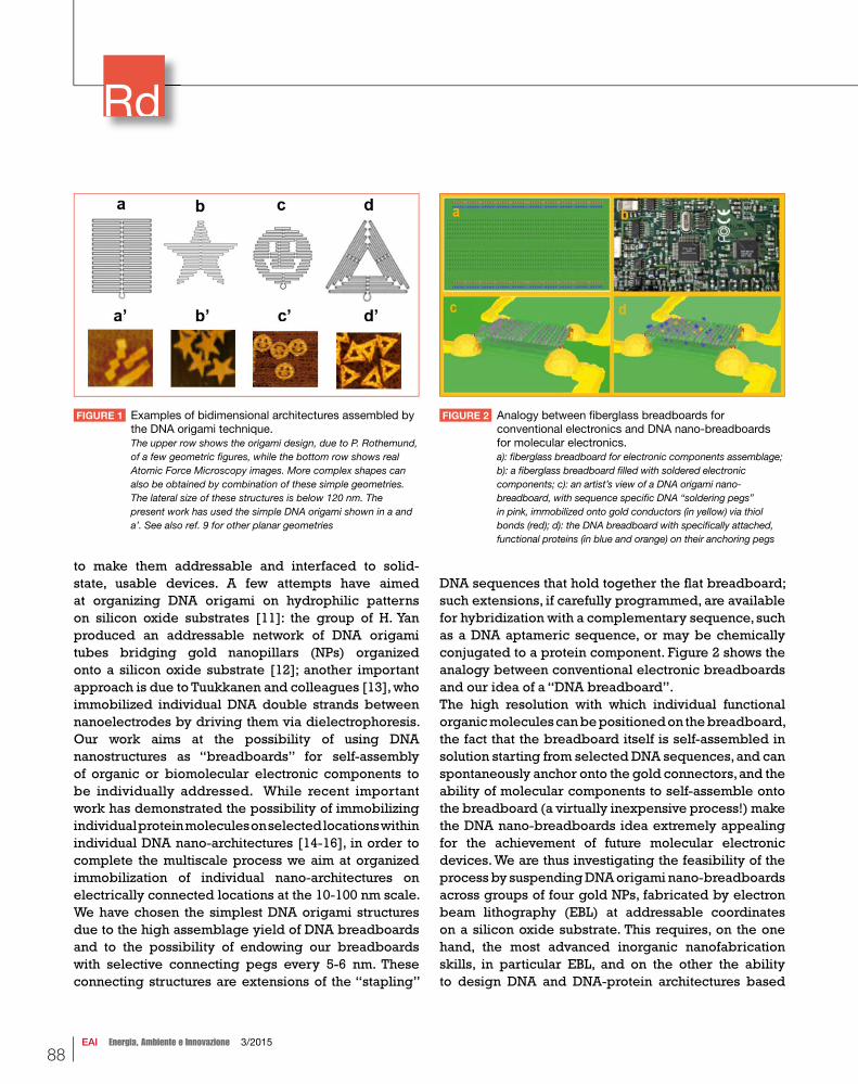
FIGURE 1 Examples of bidimensional architectures assembled by the DNA origami technique.
The upper row shows the origami design, due to P. Rothemund, of a few geometric fi gures, while the bottom row shows real Atomic Force Microscopy images. More complex shapes can also be obtained by combination of these simple geometries. The lateral size of these structures is below 120 nm. The present work has used the simple DNA origami shown in a and a’. See also ref. 9 for other planar geometries
FIGURE 2 Analogy between fi berglass breadboards for conventional electronics and DNA nano-breadboards for molecular electronics.
a): fi berglass breadboard for electronic components assemblage; b): a fi berglass breadboard fi lled with soldered electronic components; c): an artist’s view of a DNA origami nano-breadboard, with sequence specifi c DNA “soldering pegs” in pink, immobilized onto gold conductors (in yellow) via thiol bonds (red); d): the DNA breadboard with specifi cally attached, functional proteins (in blue and orange) on their anchoring pegs
Res
earc
h &
dev
elop
men
t
89EAI Energia, Ambiente e Innovazione 3/2015
on programmed single strand sequences. Finally, it requires fine control of the hybrid system self-assembly in solution, and advanced characterization techniques.
Experimental
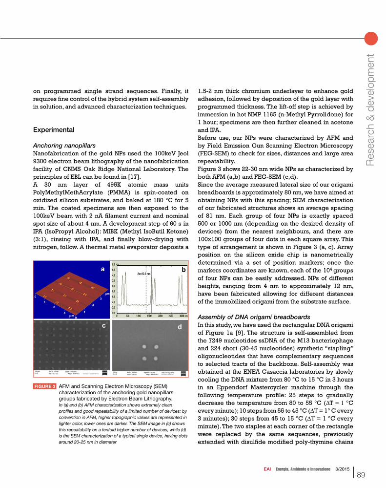
Anchoring nanopillarsNanofabrication of the gold NPs used the 100keV Jeol 9300 electron beam lithography of the nanofabrication facility of CNMS Oak Ridge National Laboratory. The principles of EBL can be found in [17]. A 30 nm layer of 495K atomic mass units PolyMethylMethAcrylate (PMMA) is spin-coated on oxidized silicon substrates, and baked at 180 °C for 5 min. The coated specimens are then exposed to the 100keV beam with 2 nA filament current and nominal spot size of about 4 nm. A development step of 60 s in IPA (IsoPropyl Alcohol): MIBK (Methyl IsoButil Ketone) (3:1), rinsing with IPA, and finally blow-drying with nitrogen, follow. A thermal metal evaporator deposits a
1.5-2 nm thick chromium underlayer to enhance gold adhesion, followed by deposition of the gold layer with programmed thickness. The lift-off step is achieved by immersion in hot NMP 1165 (n-Methyl Pyrrolidone) for 1 hour; specimens are then further cleaned in acetone and IPA.Before use, our NPs were characterized by AFM and by Field Emission Gun Scanning Electron Microscopy (FEG-SEM) to check for sizes, distances and large area repeatability.Figure 3 shows 22-30 nm wide NPs as characterized by both AFM (a,b) and FEG-SEM (c,d).Since the average measured lateral size of our origami breadboards is approximately 80 nm, we have aimed at obtaining NPs with this spacing; SEM characterization of our fabricated structures shows an average spacing of 81 nm. Each group of four NPs is exactly spaced 500 or 1000 nm (depending on the desired density of devices) from the nearest neighbours, and there are 100x100 groups of four dots in each square array. This type of arrangement is shown in Figure 3 (a, c). Array position on the silicon oxide chip is nanometrically determined via a set of position markers; once the markers coordinates are known, each of the 104 groups of four NPs can be easily addressed. NPs of different heights, ranging from 4 nm to approximately 12 nm, have been fabricated allowing for different distances of the immobilized origami from the substrate surface.
Assembly of DNA origami breadboardsIn this study, we have used the rectangular DNA origami of Figure 1a [9]. The structure is self-assembled from the 7249 nucleotides ssDNA of the M13 bacteriophage and 224 short (30-45 nucleotides) synthetic “stapling” oligonucleotides that have complementary sequences to selected tracts of the backbone. Self-assembly was obtained at the ENEA Casaccia laboratories by slowly cooling the DNA mixture from 80 °C to 15 °C in 3 hours in an Eppendorf Mastercycler machine through the following temperature profile: 25 steps to gradually decrease the temperature from 80 to 55 °C (∆T=1 °C every minute); 10 steps from 55 to 45 °C (∆T= 1° C every 3 minutes); 30 steps from 45 to 15 °C (∆T= 1 °C every minute). The two staples at each corner of the rectangle were replaced by the same sequences, previously extended with disulfide modified poly-thymine chains
FIGURE 3 AFM and Scanning Electron Microscopy (SEM) characterization of the anchoring gold nanopillars groups fabricated by Electron Beam Lithography.
In (a) and (b) AFM characterization shows extremely clean profiles and good repeatability of a limited number of devices; by convention in AFM, higher topographic values are represented in lighter color, lower ones are darker. The SEM image in (c) shows this repeatability on a tenfold higher number of devices, while (d) is the SEM characterization of a typical single device, having dots around 20-25 nm in diameter

Research & development
90EAI Energia, Ambiente e Innovazione 3/2015
(5 or 10 base long: 5T or 10T, respectively, purchased from Sigma Aldrich), to have the availability of thiol bonds at each corner attaching the nanoboard onto the gold NPs. The thiol groups attach approximately 5-10 nm from the corners of the origami along the shorter side. Both the assembly of DNA origami and the incubation on gold NPs are performed in a buffer solution (1xTAE-Mg2+) containing MgCl2 at different concentrations. A careful AFM study of our rectangular DNA origami, adsorbed on both mica and silicon oxide surfaces and thoroughly dried, has been performed aiming at a better understanding of the images of suspended DNA nanoboards.Figure 4 shows the scheme of the backbone folding and the AFM characterization, in dry condition, of a group of self-assembled DNA origami nanoboards adsorbed on the flat surface of newly cleaved mica.Most of these origami have a nearly square appearance instead of the rectangular shape observed in solution, suggesting a role of water and Mg+ ions in the dsDNA interchain spacing of the origami board. The imaged origami have a measured thickness of about 1.9 nm, which is perfectly compatible with the expected
thickness of the DNA double helix (see box 1), while their average size is 74x70 nm2.We also report, in Figure 5, a few examples of DNA origami adsorbed on the SiO2 substrate close to some groups of four NPs. Figure 5 confirms visually the size compatibility between the approximately 70-80 nm sized origami and the 81 nm NP average spacing. The average size of the SiO2 adsorbed origami from 24 different images is 70x81 nm2.
Incubation of origami solution on the nanopillars arrayThe silicon dioxide substrate surface is negatively charged, like the phosphate groups of the DNA backbone. To make adsorption possible, either on the silicon substrate or onto the gold nanopillars, the concentration of positive counterions, supplied by the dissociation of magnesium chloride in the water solution, must be adjusted. Fully neutralized charges will lead to adsorption of origami mostly on the substrate, while only partially neutralized charges, due to lower concentrations of positive Mg ions, will favour binding on the gold nanodots
FIGURE 4 a) Scheme of the DNA origami folding. The single stranded phage genome is depicted in red, while the
224 stapling oligonucleotides, approximately spaced 5-6 nm from each other, are in light green. The 5 or 10 base long chains bearing the sulphur atoms necessary for bonding on gold nanopillars are also shown
b) 3D rendering of an AFM scan of such DNA origami boards, randomly dispersed on a flat mica surface.
Some origami structures joined side by side are also observable. Light colours are for high topographic values, dark colours for low ones
FIGURE 5 AFM 3D rendering of DNA origami nanobreadboards adsorbed on a naturally oxidized silicon wafer surface on which sets of gold anchoring NPs have been fabricated by electron beam lithography.
The 80x80 nm approximate spacing of the four gold dots supplies visual information on the size compatibility between the inorganic anchoring components and the organic DNA breadboards. Same colour convention as for previous AFM scans
Res
earc
h &
dev
elop
men
t
91EAI Energia, Ambiente e Innovazione 3/2015
via the thiol bonds. We found that at a MgCl2 concentration between 75 and 100 mM, the amount of DNA origami binding on the NPs is maximized. We thus incubated 1 µl droplets of 5 nM origami solution on our NPs arrays for 40 hours in a saturated humidity chamber, then rinsed the wet specimen in ultrapure water three times before drying it in a flow of purified dry air.
Results and discussion
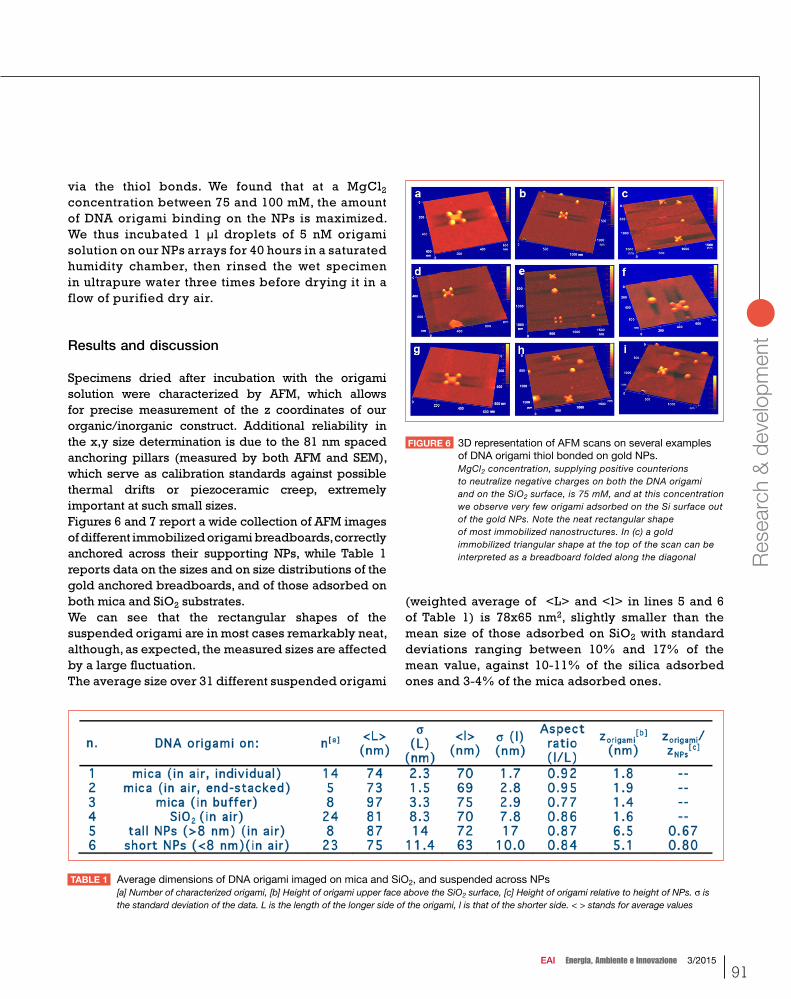
Specimens dried after incubation with the origami solution were characterized by AFM, which allows for precise measurement of the z coordinates of our organic/inorganic construct. Additional reliability in the x,y size determination is due to the 81 nm spaced anchoring pillars (measured by both AFM and SEM), which serve as calibration standards against possible thermal drifts or piezoceramic creep, extremely important at such small sizes.Figures 6 and 7 report a wide collection of AFM images of different immobilized origami breadboards, correctly anchored across their supporting NPs, while Table 1 reports data on the sizes and on size distributions of the gold anchored breadboards, and of those adsorbed on both mica and SiO2 substrates.We can see that the rectangular shapes of the suspended origami are in most cases remarkably neat, although, as expected, the measured sizes are affected by a large fluctuation. The average size over 31 different suspended origami
(weighted average of <L> and <l> in lines 5 and 6 of Table 1) is 78x65 nm2, slightly smaller than the mean size of those adsorbed on SiO2 with standard deviations ranging between 10% and 17% of the mean value, against 10-11% of the silica adsorbed ones and 3-4% of the mica adsorbed ones.
TABLE 1 Average dimensions of DNA origami imaged on mica and SiO2, and suspended across NPs [a] Number of characterized origami, [b] Height of origami upper face above the SiO2 surface, [c] Height of origami relative to height of NPs. σ is
the standard deviation of the data. L is the length of the longer side of the origami, l is that of the shorter side. < > stands for average values
FIGURE 6 3D representation of AFM scans on several examples of DNA origami thiol bonded on gold NPs.
MgCl2 concentration, supplying positive counterions to neutralize negative charges on both the DNA origami and on the SiO2 surface, is 75 mM, and at this concentration we observe very few origami adsorbed on the Si surface out of the gold NPs. Note the neat rectangular shape of most immobilized nanostructures. In (c) a gold immobilized triangular shape at the top of the scan can be interpreted as a breadboard folded along the diagonal
92EAI Energia, Ambiente e Innovazione 3/2015
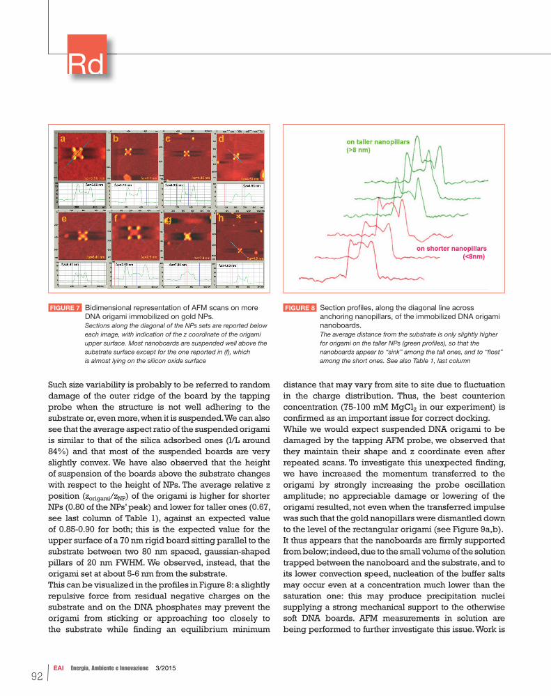
Such size variability is probably to be referred to random damage of the outer ridge of the board by the tapping probe when the structure is not well adhering to the substrate or, even more, when it is suspended. We can also see that the average aspect ratio of the suspended origami is similar to that of the silica adsorbed ones (l/L around 84%) and that most of the suspended boards are very slightly convex. We have also observed that the height of suspension of the boards above the substrate changes with respect to the height of NPs. The average relative z position (zorigami/zNP) of the origami is higher for shorter NPs (0.80 of the NPs’ peak) and lower for taller ones (0.67, see last column of Table 1), against an expected value of 0.85-0.90 for both; this is the expected value for the upper surface of a 70 nm rigid board sitting parallel to the substrate between two 80 nm spaced, gaussian-shaped pillars of 20 nm FWHM. We observed, instead, that the origami set at about 5-6 nm from the substrate.This can be visualized in the profi les in Figure 8: a slightly repulsive force from residual negative charges on the substrate and on the DNA phosphates may prevent the origami from sticking or approaching too closely to the substrate while fi nding an equilibrium minimum
distance that may vary from site to site due to fl uctuation in the charge distribution. Thus, the best counterion concentration (75-100 mM MgCl2 in our experiment) is confi rmed as an important issue for correct docking.While we would expect suspended DNA origami to be damaged by the tapping AFM probe, we observed that they maintain their shape and z coordinate even after repeated scans. To investigate this unexpected fi nding, we have increased the momentum transferred to the origami by strongly increasing the probe oscillation amplitude; no appreciable damage or lowering of the origami resulted, not even when the transferred impulse was such that the gold nanopillars were dismantled down to the level of the rectangular origami (see Figure 9a,b). It thus appears that the nanoboards are fi rmly supported from below; indeed, due to the small volume of the solution trapped between the nanoboard and the substrate, and to its lower convection speed, nucleation of the buffer salts may occur even at a concentration much lower than the saturation one: this may produce precipitation nuclei supplying a strong mechanical support to the otherwise soft DNA boards. AFM measurements in solution are being performed to further investigate this issue. Work is
FIGURE 7 Bidimensional representation of AFM scans on more DNA origami immobilized on gold NPs.
Sections along the diagonal of the NPs sets are reported below each image, with indication of the z coordinate of the origami upper surface. Most nanoboards are suspended well above the substrate surface except for the one reported in (f), which is almost lying on the silicon oxide surface
FIGURE 8 Section profi les, along the diagonal line across anchoring nanopillars, of the immobilized DNA origami nanoboards.
The average distance from the substrate is only slightly higher for origami on the taller NPs (green profi les), so that the nanoboards appear to “sink” among the tall ones, and to “fl oat” among the short ones. See also Table 1, last column
EAI 3_2015_interno.indd 92 29/07/15 16:54

Res
earc
h &
dev
elop
men
t
93EAI Energia, Ambiente e Innovazione 3/2015
in progress to devise methods to dissolve the nucleated salts trapped below the origami breadboards.Although we often observe two or three origami docked on neighbouring NP groups (see, e.g., Figures 6h and 7h), most correct dockings are spatially isolated and random events. At 75 mM concentration of MgCl2, origami adsorption on the SiO2 surface is a rather rare event, but the more frequent occurrence of correctly anchored origami on nanopillars is only of the order of 10% of the available locations; such low figure is consistent with the results obtained by Yan and coworkers [12] for DNA origami nanotubes on larger nanodots, where they observed a drop in the anchoring rate on decreasing the gold dots size below 80 nm. Being the nanometric size of the connecting NPs essential to our work, we are currently devising advanced methodologies to drive origami more efficiently to their designed locations.
Conclusions and perspectives
We have demonstrated the first fundamental step enabling the use of DNA origami breadboards for self-assembling
molecular electronic systems, i.e. the possibility of anchoring DNA nano-breadboards onto electrically-conductive nanopillars. The origami technique gives us the possibility, for the type of breadboards used in this work, to self-assemble organic components with a resolution of about 6 nm. We have also demonstrated the possibility of suspending origami across tall nanopillars (in the range of 8-15 nm). If the space between the suspended origami and the substrate is clear, this may be exploited to obtain DNA breadboards for dual face organization of components; for the DNA origami used in this work, we can imagine up to about 400 organic components for each device of approximately 70x80 nm2. We need however to explore methods to avoid nucleation and coalescence of buffer salts nanocrystals under the boards.The most important envisageable advantage of this methodology is certainly its use for cheap self-assembly of complex architectures of organic components on truly nanometrically selected locations, simply by the careful design of the DNA sequences. It should be remarked however that, as shown, a process based only on random docking of origami on their gold anchoring nanopillars has a rather low rate of occurrence and does not ensure
FIGURE 9 3D representation, and section profiles along the displayed blue lines, of the anchored DNA origami shown in Figure 7g. (a) as normally imaged by AFM gentle tapping; and (b) after 3 scans with strong impulse transfer (increased cantilever oscillation amplitude). In (b)
the gold nanopillars have been dismantled by the “hammering” probe, while the height of the origami remains the same
EAI 3_2015_interno.indd 93 29/07/15 16:54
Research & development
94EAI Energia, Ambiente e Innovazione 3/2015
site selectivity nor even geometric positional or angular precision. On the contrary, the observed low yield of correctly docked nanoboards is largely due to the small size of the anchoring nanopillar, which is a necessary issue of any nanotechnological approach. An important extension of this research will therefore be directed to increasing the yield of binding on even smaller (but still technologically feasible) anchoring pillars by electrical methods exploiting electrically connected NPs. This will also allow site-specific immobilization of nano-breadboards by the sequential introduction of different DNA origami. Furthermore, as a next step, site-selective docking of individual organic components within each nanoboard will exploit the specific binding capabilities offered by small DNA aptameric sequences, which can be easily hybridized to the extensions of the origami stapling oligonucleotides.
AcknowledgmentsThis work was performed with partial funding from the European Union IRSES scheme META Project and under User Projects of the Center for Nanophase Materials Science at the Oak Ridge National Laboratory. We thank the Danish National Research Foundation (DNRF81) for financial support to the Center of DNA Nanotechnology. We are also indebted to Dr. C. Cantale for very helpful discussions and collaboration. l
Liqian Wang1,2, Claudia Dalmastri1, Bruno Rapone1, Scott Retterer4, Abhichart Krissanaprasit3, Kurt Gothelf3, Piero Morales1,2
1 ENEA, Casaccia Research Centre, Rome, I2 Centro NAST, University of Tor Vergata, Rome, I
3 cDNA Center, University of Aarhus, DK4 Center for Nanoscale Materials Science, Oak Ridge National Laboratory,
Oak Ridge, TN (USA)
refe
ren
ce
s [1] Thomas H. LaBean (2006): “Finite-size, fully addressable DNA tile lattices formed by hierarchical assembly procedures”. Angewandte Chemie Int. Ed., 45, 735
[2] E. Winfree, F. Liu, L. A. Wenzler, N. C. Seeman (1998): “Design and self-assembly of two-dimensional DNA crystals”. Nature, 394, 539
[3] C. Mao, W. Sun, N. C. Seeman (1999): “Designed two-dimensional DNA Holliday junction arrays visualized by atomic force microscopy”. J. Am. Chem. Soc., 121, 5437
[4] T. H. LaBean, H. Yan, J. Kopatsch, F. Liu, E. Winfree, J. H. Reif, N. C. Seeman (2000): “Construction, analysis, ligation, and self-assembly of DNA triple crossover complexes”. J. Am. Chem. Soc., 122, 1848
[5] H. Yan, S. H. Park, G. Finkelstein, J. H. Reif, T. H. LaBean (2003): “DNA-templated self-assembly of protein arrays and highly conductive nanowires”. Science, 301, 1882; S. H. Park, P. Yin, Y. Liu, J. H. Reif, T. H. LaBean, H. Yan (2005): “Programmable DNA self-assemblies for nanoscale organization of ligands and proteins”. Nano Lett., 5, 729
[6] D. Liu, S. H. Park, J. H. Reif, T. H. LaBean (2004): “DNA nanotubes self-assembled from triple-crossover tiles as templates for conductive nanowires”. Proc. Natl. Acad. Sci. USA, 101, 717
[7] D. Liu, M.S. Wang, Z.X. Deng, R. Walulu, C.D. Mao (2004): “Tensegrity: Construction of rigid DNA triangles with flexible four-arm DNA junctions”. J. Am. Chem. Soc., 126, 2324
[8] B. Ding, R. Sha, N. C. Seeman (2004): “Pseudohexagonal 2D DNA crystals from double crossover cohesion”. J. Am. Chem. Soc., 126, 10230
[9] P. W. K. Rothemund (2006): “Folding DNA to Create Nanoscale Shapes and Patterns”. Nature, 440, 297
[10] H. T. Maune, S. Han, R. D. Barish, M. Bockrath, W. A. Goddard III, P. W. K. Rothemund, E. Winfree (2010): “Self-assembly of carbon nanotubes into two-dimensional geometries using DNA origami templates”. Nat. Nanotechnol., 5, 61
[11] R. J. Kershner, L. D. Bozano, C. M. Micheel, A. M. Hung, A. R. Fornof, J. N. Cha, C. T. Rettner, M. Bersani, J. Frommer, P. W. K. Rothemund, G. M. Wallraff(2009): “Placement and orientation of individual DNA shapes on lithographically patterned surfaces”. Nat. Nanotechnol., 4, 557; A. M. Hung, C. M. Micheel, L. D. Bozano, L. W. Osterbur, G. M. Wallraff, J. N. Cha (2010): “Large-area spatially ordered arrays of gold nanoparticles directed by lithographically confined DNA origami”. Nat. Nanotechnol., 5, 121
[12] B. Ding, H. Wu, W. Xu, Z. Zhao, Y. Liu, H. Yu, H. Yan (2010): “Interconnecting Gold Islands with DNA Origami Nanotubes”. Nano Lett., 10, 5065
[13] S. Tuukkanen, A. Kuzyk, J. J. Toppari, H.Häkkinen, V. P.Hytönen, E. Niskanen, M. Rinkiö, P. Törmä (2007): “Trapping of 27 bp-8 kbp DNA and immobilization of thiol-modified DNA using dielectrophoresis”. Nanotechnology, 18, 295204
[14] N. V. Voigt, T. Tørring, A. Rotaru, M. F. Jacobsen, J. B. Ravnsbæk, R. Subramani, W. Mamdouh, J. Kjems, A. Mokhir, F. Besenbacher, K. V. Gothelf (2010): “Single-molecule chemical reactions on DNA origami”. Nat. Nanotechnol., 5, 200
[15] H. Li,T. H. LaBean and D. J. Kenan (2006), “Single-chain antibodies against DNA aptamers for use as adapter molecules on DNA tile arrays in nanoscale materials organization”. Org. Biomol. Chem., 4, 3420
[16] M. Tintoré, I. Gàllego, B. Manning, R. Eritja, C. Fàbrega (2013): “DNA Origami as a DNA Repair Nanosensor at the Single-Molecule Level”. Angew. Chem. Int. Ed., 52, 7747
[17] M.Koehler, W. Fritsche (2007): Nanotechnology. An Introduction to Nanostructuring Techniques. Wiley-VCH Verlag GmbH & Co. KGaA, Weinheim
EAI 3_2015_interno.indd 94 29/07/15 16:54