creating)ausable)power)supply)from)asolar)panel)ausable)power)supply)from)asolar)panel)...
TRANSCRIPT
Creating a Usable Power Supply from a Solar Panel An exploration in DC-‐DC converters
By Kathleen Ellis Advised by Dr. Derin Sherman Department of Physics, Cornell College
November 21, 2012
Introduction
Over the course of the past couple of decades solar power has become more and more attractive due to the increased awareness of environmental issues and emphasis on sustainability. However with relatively low conversion efficiencies and low power outputs solar power is impractical for many applications. For this reason it is extremely important to efficiently convert the solar output into a usable form of power.
There are two major problems with using the output that comes directly from solar panels. Firstly they tend to output higher DC (Direct Current) voltage than most loads use. The panel I had to work with was rated at 18 volts 0.3 amps DC at maximum power. The most common forms of power are wall outlets and more recently charging devices via USB port. Wall outlets provide 120 volts AC (alternating current) and USB ports provide 5 volts DC. These are both very different forms than a direct current 18 volt source. No electronics that need either of the two most common power supplies are able to directly use the solar output.
The second problem is the fact that the solar panel will only output its rated power on a sunny day and even then the voltage and current output of the panel is at the mercy of the clouds. I found that even small clouds can drastically affect the output of the solar panel. A fluctuating power supply is also very undesirable for any kind of electronic device that might be hooked up to the solar panel.
These two problems outlined above were what I set out to solve over the course of this project. I decided on a USB (5 volt DC) power supply instead of a 120 AC power supply because of the power output of the solar panel I was working with. Since a USB port supplies 5 volts and between 0.5 and 1.5 amps depending on the type of USB port [2], the goal of this project was to create a relatively constant 5v power supply that could output between 0.5 and 1 amp. Theoretically this power supply would be used to provide free solar powered USB charging ports around campus for the Cornell community to use. This paper explores the theory behind different types of DC-‐DC converters and how they performed in this project.
Theory
DC-‐DC Conversion
In order to change the voltage that the solar panel is putting out to 5 volts it is necessary to temporarily store energy somewhere in order to release it to the load at a different voltage. This is usually done by storing the energy in either an electric field (using capacitors) or a magnetic field (using inductors) but can also be done using a transformer (also uses a magnetic field) if you convert the DC voltage into AC before raising or lowering the voltage. In the case of solar panels we are only interested in converting the voltage down to 5 volts because when the solar panel is outputting less than 5 volts it does not output enough power to provide over 0.5 amps. In this section the theory and circuit diagrams of different DC-‐DC converters are discussed as well as the feasibility in application to solar panels.
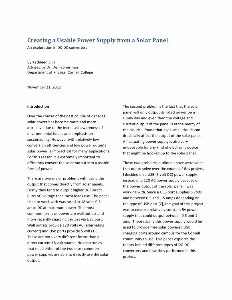
Transformer
A transformer is really an AC to AC converter that can be used for DC by converting the DC power into AC and then the AC back into DC. The advantage of the transformer converter is that the ratio of the input voltage to the output voltage can be chosen by changing the ratio of the number of turns on the primary winding to the number of turns on the secondary winding as is illustrated by the equation:
!!!!=!!!!
The transformer converter is ideal for applications where the input needs to be electrically isolated from the output of the circuit because the input and output are only connected via a magnetic field. The fact that there is no electrical contact is necessary for some applications. [3]
However for the purpose of this project the transformer is not the the most promising converter because it would waste power converting to AC and back.
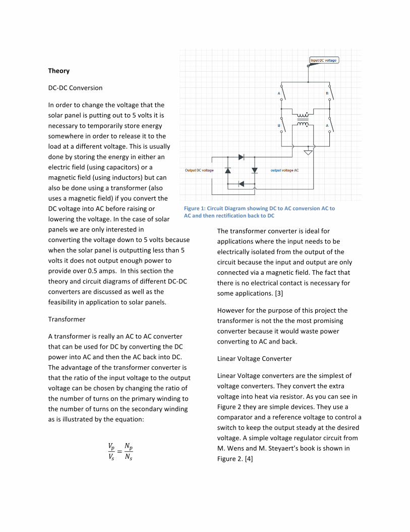
Linear Voltage Converter
Linear Voltage converters are the simplest of voltage converters. They convert the extra voltage into heat via resistor. As you can see in Figure 2 they are simple devices. They use a comparator and a reference voltage to control a switch to keep the output steady at the desired voltage. A simple voltage regulator circuit from M. Wens and M. Steyaert’s book is shown in Figure 2. [4]
Figure 1: Circuit Diagram showing DC to AC conversion AC to AC and then rectification back to DC

The Linear Voltage Converter is useful in applications where you are worried about space because inductors and capacitors are more bulky than resistors. However the goal of this project is efficiency not space. Wasting the precious solar energy into heat it is not a very efficient way to convert voltage. In the case of this project, it does not align with our goals.
Buck Converter
Buck converters use a combination of an inductor and capacitor to store energy in a magnetic field and electric field. A circuit diagram of a basic buck converter is shown in Figure 3. When the switch is closed the inductor and capacitor are charged by the input voltage, in this case a solar panel. The output current comes through the inductor into the load. When the switch is closed the inductor opposes the change in current so it discharges it's energy into the load until it has no more energy stored in it's magnetic field. If the switching speed of the circuit is low enough that the inductor is allowed to fully discharge the capacitor takes over in supplying voltage and current to the load until it is fully discharged.
In general in Buck converters the duty cycle of the switch signal is proportional to the ratio of output voltage to input voltage as is demonstrated by the following equation:
!!"#!!"
= !"#$ !"#$% = !!"!
Where Ton is the time the switch is on per cycle and T is the time per cycle. Assuming the converter was perfect and had no internal resistances due it's components the current and voltage would be related by the following equation [2 Jaycar]
!!"!!"#
= !!"#!!"
The current draw and resistance of the load are also important aspects to consider when designing a buck converter. If the duty cycle and switching frequency are constant the amount of ripple in the output voltage is determined by the time constant of the RC circuit created between the capacitor and load resistance. In order to produce a small amount of ripple the time constant should be very large compared to the period of the signal frequency. [1] Since the buck converter does not waste power to heat through a resistor or creating an alternating current it would make a good choice for the purposes of solar power conversion.
Switched Capacitor Converter
Switched Capacitor (SW) Converters, also referred to as charge pumps, use only capacitors to step down or step up the voltage. In this case we are only interested in stepping down the voltage for reasons discussed earlier. The idea is to temporarily store energy in the electric field of the capacitors while the configuration of the circuit is switched and then release this energy into the load in a different
Figure 2: A simple Linear Series Voltage Converter
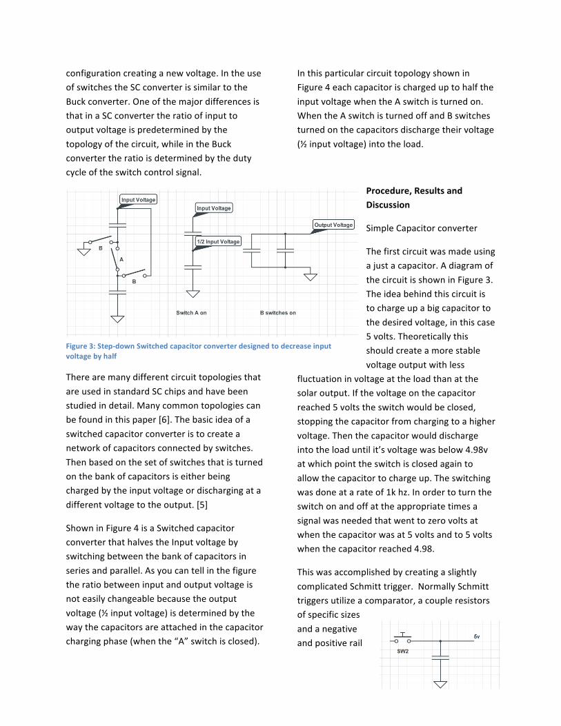
configuration creating a new voltage. In the use of switches the SC converter is similar to the Buck converter. One of the major differences is that in a SC converter the ratio of input to output voltage is predetermined by the topology of the circuit, while in the Buck converter the ratio is determined by the duty cycle of the switch control signal.
There are many different circuit topologies that are used in standard SC chips and have been studied in detail. Many common topologies can be found in this paper [6]. The basic idea of a switched capacitor converter is to create a network of capacitors connected by switches. Then based on the set of switches that is turned on the bank of capacitors is either being charged by the input voltage or discharging at a different voltage to the output. [5]
Shown in Figure 4 is a Switched capacitor converter that halves the Input voltage by switching between the bank of capacitors in series and parallel. As you can tell in the figure the ratio between input and output voltage is not easily changeable because the output voltage (½ input voltage) is determined by the way the capacitors are attached in the capacitor charging phase (when the “A” switch is closed).
In this particular circuit topology shown in Figure 4 each capacitor is charged up to half the input voltage when the A switch is turned on. When the A switch is turned off and B switches turned on the capacitors discharge their voltage (½ input voltage) into the load.
Procedure, Results and Discussion
Simple Capacitor converter
The first circuit was made using a just a capacitor. A diagram of the circuit is shown in Figure 3. The idea behind this circuit is to charge up a big capacitor to the desired voltage, in this case 5 volts. Theoretically this should create a more stable voltage output with less
fluctuation in voltage at the load than at the solar output. If the voltage on the capacitor reached 5 volts the switch would be closed, stopping the capacitor from charging to a higher voltage. Then the capacitor would discharge into the load until it’s voltage was below 4.98v at which point the switch is closed again to allow the capacitor to charge up. The switching was done at a rate of 1k hz. In order to turn the switch on and off at the appropriate times a signal was needed that went to zero volts at when the capacitor was at 5 volts and to 5 volts when the capacitor reached 4.98.
This was accomplished by creating a slightly complicated Schmitt trigger. Normally Schmitt triggers utilize a comparator, a couple resistors of specific sizes and a negative and positive rail
Figure 4: Simple capacitor charging circuit
Figure 3: Step-‐down Switched capacitor converter designed to decrease input voltage by half

voltage. The problem was that in the solar circuit there was no negative voltage source because it was powered solely by the solar panel. Because of this slight complication a configuration using two 311 comparators was used.1
In the beginning one of the problems with this circuit was what to use as a switch. In a standard MOSFET the gate voltage needs to be 5-‐10 volts higher than the drain. This was not possible to do because the gate was driven by a logic signal (0 or 5 volts) from a 555 oscillator and the drain voltage also needed to be 5 volts. For this reason the solid-‐state relay chip LH1511 was used. This type of relay chip uses an LED to activate photodiodes so the control signal just needs to be enough to turn on the LED.
After the circuit worked inside I took it outside to test the circuit under real conditions, on a sunny day in November the capacitor output 0.02A. This is less than 5% of the rated output of a USB port. With this kind of performance this circuit was discarded because the capacitor was not outputting enough current to charge any kind of device.
Difficulties
After the single capacitor circuit was rejected the idea of a switched capacitor converter was proposed and built. However after a couple days of troubleshooting the converter was still not working. As a desperate attempt a transformer converted was built according to the circuit described in the theory section. The transformer ended up being the wrong size for
1 The Schmitt trigger circuit configuration was obtained in Dr. Derin Sherman’s graduate thesis which can be found here: http://dspace.mit.edu/handle/1721.1/33487
the desired conversion. After these missteps it was discovered that the breadboard of the original switched capacitor circuit was shorted. The circuit worked when moved to a new breadboard.
The Final Circuit
The final circuit was a switched capacitor parallel-‐series step-‐down converter. As you can see in Figure 6 the circuit is very similar to the circuit described earlier in the theory section. However since the solar panel puts out 18 volts it is necessary to third the voltage instead of halve it. Other than the step-‐down ratio the circuit works the same as the example. When the “A” switches are closed the capacitors are in series connected to the solar panel causing them to each charge up to 1/3 the input voltage, in this case 6 volts. When the “B” switches are closed the capacitors are hooked up in parallel and to the holding capacitor. In phase B the holding capacitor is charged with 6 volts. The circuit is shown in Figure 5.
The idea in this circuit is to output triple the current that the solar panel was outputting. As each capacitor charges up at the voltage and current of the solar panel and then discharges at the same current but now there are 3 capacitors all outputting the solar current which
Figure 5: The final switched capacitor circuit. When A switches are closed the three capacitors are connected in series. When B switches are closed the three capacitors are connected in parallel.

creates triple the current going to the holding capacitor.
The problem with the circuit as I have described it is that the holding capacitor is only charging for the time that the “B” switches are on. In order to fix this problem another bank of capacitors was add with the identical switch configuration. The two circuits were timed so that when one bank was discharging into the holding capacitor the other bank was charging from the solar panel and vice verse. In this configuration there was always a capacitor bank providing current to the holding capacitor.
In the final circuit two banks of capacitors were used with two SC converters. The capacitors used in the capacitor banks were 470μF. The holding capacitor was a 0.06F capacitor. The switches were solid-‐state relay chip LH1511. The chips were hooked up in AC mode. The switches were turned on and off by a 555 oscillator and a not gate. The not gate was needed because when some switches were receiving the on signal (5 volts) others needed an off signal (0 volts) and vice versa. A linear voltage regular was used to power the not gate and the 555 oscillator. While this wasted power it was necessary to have 5 volts to run these chips.
On a relatively sunny day the holding capacitor outputted 0.15 amps at 4 volts. While this was greater than the output current of the original circuit it was far less than ideal. Especially considering that the solar panel was also outputting 0.15 amps. For some reason the tripling of the current was not happening. The voltage on the capacitor also fluctuated depending on the output of the solar panel.
The final circuit did not tripling the current as expected. Possible problems were the solar panel not outputting it’s rated current at maximum power, the circuit was not operated in the maximum power range of the solar panel, too much power was being used by the circuit elements, and the load resistance and current
draw was not accounted for in the design of the circuit. Most likely some combination of these factors was creating the less than ideal output current and voltage of the final circuit configuration.
Conclusion
In the end none of the circuits that were built met the goals of the project. It turned out that the most difficult part was outputting enough current. Using a larger solar panel could solve this problem, however this option would satisfy the goal of efficiency. Future work
A more detailed analysis of the current flow through the switched capacitor circuit including the holding capacitor and load resistance is needed in order to understand what is going wrong and make a circuit that can meet the goals. Further research into any of the problems mentioned in the final circuit section would greatly help improve the performance of the circuit.
A true Buck converter was never implemented over the course of the project. The Buck-‐converter should be considered as a viable way to meet the goals of the project. Theoretically it should be possible to regulate the output voltage via duty cycle depending on the input coming from the solar panel. It would allow for a more constant voltage and hopefully boosted current flow to the load if properly designed.
Another interesting avenue of research would be to create a converter that outputted 120 volts alternating current. This would need a larger solar panel to be able to generate enough current. However it would also be a usable form of power.

References
[1]University of Technology Sydney. Step-‐down Buck converter: Ideal circuit. 1999. http://services.eng.uts.edu.au/~venkat/pe_html/contents.htm (accessed 2012).
[2]Anthony, Sebastian. Extreme Tech. January 24, 2012. http://www.extremetech.com/computing/115251-‐how-‐usb-‐charging-‐works-‐or-‐how-‐to-‐avoid-‐blowing-‐up-‐your-‐smartphone (accessed November 19, 2012).
[3] Jaycar Electronics. "Jaycar Electronics Reference Datasheet." 2001. http://www.jaycar.com.au/images_uploaded/dcdcconv.pdf (accessed November 20, 2012).
[4]M. Wens, M. Steyaert. "Basic DC-‐DC Converter Theory." In Design and Implementation of Fully-‐Integrated Inductive, 27-‐63. DOI 10.1007/978-‐94-‐007-‐1436-‐6_2: Springer Science+Business Media, 2011.
[5] M.D Seeman. A Design Methodology for Switched-‐Capacitor DC-‐DC Converters. Graduate thesis University of California Berkley. 2009
[6] M.D Seeman, S Sanders. “Analysis and Optimization of Switched-‐Capacitor DC–DC Converters”. IEEE TRANSACTIONS ON POWER ELECTRONICS, VOL. 23, NO. 2, MARCH 2008.