cs8 technical manual - ddaconsoles.com · cs8 service manual telex communications (uk) limited in...
TRANSCRIPT

CS8 Service Manual
Klark Teknik Building Walter Nash Road
Kidderminster Worcestershire
DY11 7HJ
Tel: +44 (0) 1562 741515 Fax: +44 (0) 1562 745371
Email: [email protected]
Website: www.ddaconsoles.com
CS8 Service Manual Telex Communications (UK) Limited
In line with the company’s policy of continual improvement, specifications and function maybe subject
to change without notice. This Operator Manual was correct at the time of writing. E&OE.

2

3
ContentsINTRODUCTION ......................................................................................... 4CS8 SPECIFICATIONS................................................................................. 9OPTIONS ...................................................................................................... 9CS8 DIMENSIONS AND WEIGHTS ........................................................ 10DECLARATION OF CONFORMITY........................................................ 11INSTALLATION GUIDE ............................................................................. 12ATTENTION ............................................................................................... 13CIRCUIT DESCRIPTIONS.......................................................................... 14INPUT MODULE (CD1279) ..................................................................... 14INPUT MODULE LINKS ........................................................................... 19INPUT MODULE BLOCK DIAGRAM ..................................................... 20THE STEREO INPUT MODULE (CD1302/3).......................................... 21STEREO INPUT LINKS.............................................................................. 25STEREO INPUT MODULE BLOCK DIAGRAM ..................................... 26THE GROUP OUTPUTS (CD1280/CD1286) .......................................... 27GROUP OUTPUT LINKS (MATRIX)........................................................ 31GROUP OUTPUT LINKS (RETURN) ....................................................... 32GROUP OUTPUTS 1-6 BLOCK DIAGRAM ........................................... 33GROUP OUTPUTS 7-8 BLOCK DIAGRAM ........................................... 34THE MASTER MODULE........................................................................... 35MASTER MODULE LINKS....................................................................... 39MASTER MODULE BLOCK DIAGRAM ................................................. 41THE BUS LINKING PORT ......................................................................... 42THE METERBRIDGE................................................................................. 43THE POWER SUPPLY ............................................................................... 45BUS CONNECTOR PIN OUT ................................................................... 47CS8 MATRIX CONNECTOR ..................................................................... 48BUS LINK CONNECTOR.......................................................................... 49CS8 PARTS LISTING.................................................................................. 50SERVICE INFORMATION......................................................................... 58CS8 CIRCUIT DIAGRAMS........................................................................ 60
The information in this manual has been carefully verified and is believed to becorrect, however, EVI Pro Audio reserves the right to modify the productdescribed in this manual at any time. This document may not be copied orreproduced by any method whatsoever, whether in part or in whole, withoutthe written permission of EVI Pro Audio.
© Copyright 1997 EVI Pro Audio Group. All rights reserved.
Manual Version DOC03-CS12M/A.
4
INTRODUCTION
The CS8 console has been designed to provide the consultant,contractor, installer and user with a cost effective system whichwill perform to accepted professional standards, be simple for theuntrained user to operate, and be tolerant of wiring and installationproblems. There can be no excuse for a system which is over sensitiveto the wiring and installation conventions used, and hums at everyopportunity.
High quality balanced inputs and outputs are only part of the story.Equally important is the way in which the console grounding systemworks, because it is through the console ground that all the noisyground currents from the cable screens will flow. Any part of theaudio signal path which shares the cable screen to console groundpath within the console will effectively have the cable screen noiseadded to that signal path. The current flowing in cable shields intypical installations has be shown to be substantial (in the order of100mA and above) and is caused by the difference in potentialbetween the ground connection at each end of the cable screens.
Of comparable importance to any system performance is the powersupply. Internal linear power supplies may be less expensive, butare usually responsible for inducing noise into the audio andgenerating substantial amounts of heat, making it uncomfortablefor the operator. Internal switch mode supplies may be cool running,but are usually even more of a problem with regard to noise.Another often overlooked point with internal power supplies ishow to provide auto-switchover between 2 supplies withoutextensive modification thereby nullifying the warranty. Internalsupplies are also a potential problem from a maintenance point ofview.
Most service technicians can easily fault find and repair a linearsupply with commonly found components, but a switch mode supplydoes not make use of common off the shelf components. Althoughmore expensive, a separate and generously rated linear powersupply is used with the CS8 keeping heat and noise away from theconsole. Rack mounting ears are available for permanentinstallations, and the supply is UL and CSA approved.
At this point it is useful to look at some of the features of the CS8.
PAN AND ROUTINGThe pan pot can be switched between stereo panning mode, andleft/centre/right panning mode. Left-centre-right panning to themaster outputs provides much improved spatial positioning. Thetechnique has been used for many years in the film industry whereits benefits are well known.

5
In music systems the centre channel generates a more solid centreimage, especially for the “star” of the show, and helps to maintaina stereo image across a wider sound stage. In mixed mediaproductions and in church applications the use of a speech optimisedcentre cluster can improve intelligibility without compromising themusic system performance.
If only a stereo system is being run, and the pan pot is switched tostereo mode, then the centre output is individually assignable fromeach input or the from a sum of the left/right mix to provide aseparate mono output for broadcast/film feeds etc.
Another unique feature for a mixer in this class is individual subgroup routing instead of the inconvenient and inflexible pairedrouting which always requires the use of the pan pot to route achannel to a single sub group. There is always a crosstalkperformance compromise involved and it is done solely for economicrather than for operational reasons, as it halves the number ofrouting switches and removes the need for a pan in/out switch.The CS8 allows routing to the sub groups either individually or inpairs via the pan pot.
EQUALISATIONThe CS8 input module has a 4 band equaliser with high and lowfrequency boost/cut controls and two swept frequency middlesections. There is more than two octaves of overlap between thefrequency ranges of the mid equalisers while the frequency spanextends to from 70Hz to 10kHz.
AUXILIARIESThe CS8 has 8 full time auxiliary send controls allowing easy sessionsetup. These are normally post fade but can be switched pre fade.Normally the pre fade signal is pre fade post cut but byusing internallinks it can be changed to the pre equaliser signal. Auxiliaries 7 and8 can be used in stereo where stereo foldback, for example, isrequired.
CHANNEL CUTThe channel cut is a silent FET switch which can be remotelycontrolled through a connector on the rear of each channel by asimple connection to ground. In addition, when the channel cutswitch is pressed, another contact is grounded on the Mute Remoteconnector. This can be used to control a Midi Mute controller, cuelights, or even to control another channel on the mixer by linkingthe mute out pin of one channel to the mute in pin of any otherchannel(s). Such an application could be a podium switch whichwould allow the speaker to override other channels for example.

6
SOLO/PFL MONITORINGWhile it is normal to find PFL/AFL on almost all mixers, the CS8goes a step further. The input solo is arranged to have priority overthe output solo. This means that there is no need to de-select anoutput solo when selecting one or more input solo controls, andwhen the input solo is released, the output solo is re-established. Amaster solo level trim control is located on the master module forlevel matching, and the level of the solo signal is displayed on theleft mix bargraph.
An additional solo feature provided is Solo In Place. In this mode,soloing any input channel will cause all other input channels to becut, thereby allowing only itself to be heard in the mix, correctlypanned and at the right level, along with any stereo effect returnchannels. This is of great benefit during set-up and rehearsal and ismuch more useful than the standard PFL. A switch on the mastermodule selects Solo In Place mode.
SIGNAL LED’sThe value of effective metering of signal levels throughout thesignal path cannot be overestimated. Signal present and 0dB LED’son all input channels give confidence to the operator while peakoverload LED’s indicate when the channel is being driven close toclipping. However, it is unusual to find a peak overload LED at thevery place where it is most needed, at the summing bus mixamplifiers, operating independently of the output meters. If themix amplifier is overloaded and starts to clip, the only thing thatcan be done to rectify the situation is to pull down all input faders.On the CS8, there are overload warning LED’s on each of the subgroup mix amplifiers as well as on the left, centre and right mixamplifiers. When the output meters are switched to observe thematrix outputs the bus peak leds also monitor the matrix bus.
INSERTSInserts are used to patch in external pieces of equipment such asequalisers, limiters etc. and are provided on all channels, groupoutputs, mix outputs and auxiliary outputs. To be useful anduseable, the inserts should be at a level which is compatible withthis external equipment. Sadly, this is often not the case. Somemixers have inserts at odd levels which will preclude their efficientuse because of the noise penalty. All inserts on the CS8 are at aconsistent level which is at the internal operating level of 0dBu.
AUXILIARY INSERTSIn most installations, it is quite normal to place an equaliser in thestage monitor sends, but this is normally external to the mixer. Thisof course means that the only way of listening to the monitor sends(internal to the mixer) is via the solo system.

7
Herein lies a problem. The operator does not hear the effect of theexternal equalisation. Also, any noise introduced by the externaldevice is constant and not proportional to the setting of the sendcontrol. The ideal place to insert an external device is pre the sendmaster control and this is the case in the CS8.
EQUALISER CURVESThe following graphs illustrate the equalisation and filteringresponses of the CS8 console.
CS8HFLF HF/LF EQUALISER RESPONSECS8MID MID FREQUENCY EQUALISER BANDWIDTH
ADJUSTMENTCS8MID1 MID FREQUENCY EQUALISER AMPLITUDE
ADJUSTMENTCS8MID2 MID FREQUENCY EQUALISER FREQUENCY
ADJUSTMENTCS8HP HIGH PASS FILTER RESPONSE

8
20 100 1k 10k 20k
FREQ(Hz)
-20.00
-15.00
-10.00
-5.000
0.0
5.0000
10.000
15.000
20.000AMPL(dBr)AUDIO PRECISION CS8HIMID vs 11 APR 97 11:37:11 THE HI-MID FREQUENCY
EQUALISER RESPONSESHOWING FREQUENCYRANGE
THE HIGH AND LOWFREQUENCY EQUALISERRESPONSE
20 100 1k 10k 20k
FREQ(Hz)
-20.00
-15.00
-10.00
-5.000
0.0
5.0000
10.000
15.000
20.000AMPL(dBr)AUDIO PRECISION CS8HFLF vs 11 APR 97 11:31:21
20 100 1k 10k 20k
FREQ(Hz)
-20.00
-15.00
-10.00
-5.000
0.0
5.0000
10.000
15.000
20.000AMPL(dBr)AUDIO PRECISION CS8LOMID vs 11 APR 97 11:41:51 THE LO-MID FREQUENCY
EQUALISER RESPONSESHOWING FREQUENCYRANGE
20 100 1k 10k 20k
FREQ(Hz)
-20.00
-15.00
-10.00
-5.000
0.0
5.0000
10.000
15.000
20.000AMPL(dBr)AUDIO PRECISION CS8HPF vs 11 APR 97 11:43:15 THE HIGH PASS FILTER
RESPONSE.

9
CS8 SPECIFICATIONS
Nominal Operating Level +4dBu with a unity gain structure.
Frequency Response 20Hz - 20kHz +/-0.5dB any input to any outputat a gain < 50dB.
EQ rangeHF +/-15dB @ 10kHz shelvingLF +/-15dB @ 100Hz shelvingHi Mid +/-15dB 470Hz - 15kHz, Q = 1.4Lo Mid +/-15dB 70Hz - 2.2kHz, Q = 1.4
Channel Routing Attenuation > 90dB @ 1kHzChannel Mute Attenuation > 95dB @ 1kHzChannel Fader Attenuation > 85dB @ 1kHz
Distortion0.005% @1kHz any input to any output at a gain < 50dB.
Noise: -82dBu (24 channels routed and cut)EIN: -127.5dBu ref 200 ohmsEIN: -128.7dBu ref 150 ohms
Maximum output level: +20dBu into a bridging loadOutput impedance: <75RMaximum input level: +30dBuPhono connector levels:Nominal -10dBV
Signal present threshold: -21dBuPeak led threshold: 3dB below clipping
Power consumption: < 600 Watts
OPTIONS
Input transformers Multipole connectorsOutput transformers Bus linking cableLED Meterbridge Flight caseVU Meterbridge Spare power supply with autoFlight Case switchover

10
CS8 DIMENSIONS AND WEIGHTS
32 CHANNEL 1432.50mm(56.40")
40 CHANNEL 1681.50mm(66.20")
48 CHANNEL 1930.50mm(76.00")
MASTER AND OUTPUT SECTION
16 CHANNEL 934.50mm(36.70")
24 CHANNEL 1183.50mm(46.60")
4 S
TE
RE
O
MO
DU
LES
Meterbridge Widths:VU 46.6 inches/1183.5mm (This cannot be fitted to a 16 input console)LED As per corresponding console width.
Console weights (packed):
16 26.4kg/58lbs LED m/b4.7kg/10.4lbs Combined 31.1kg/68.4lbs24 36kg/80lbs LED m/b6.0kg/13.3lbs Combined 42.0kg/93.3lbs32 45.6kg/100lbs LED m/b7.4kg/16.3lbs Combined 53.0kg/116.3lbs40 55.2kg/122lbs LED m/b8.6kg/19.0lbs Combined 63.8kg/141lbs48 64.8kg/143lbs LED m/b10.0kg/22.0lbs Combined 74.8kg/165lbs
VU Meterbridge 6.5kg/14.5lbs (Add to weight without LED meterbridge)
These weights assume a fully fitted console. Meterbridges are shipped in withthe console but not mounted on the console.
Power Supply Weight (packed): 7.8kg(17.2lbs)Dimensions: 2U Rack Mounting with a depth of 265mm(10.43")
DIMENSIONS AND WEIGHTS

11
Declaration of Conformity
The Manufacturer of the Products covered by this Declaration is
Klark Teknik Building, Walter Nash Road, Kidderminster,Worcestershire, DY11 7HJ.
The Directives Covered by this Declaration.89/336/EEC Electromagnetic Compatibility Directive, amended by 92/31/EEC & 93/68/EEC
73/23/EEC Low Voltage Equipment Directive, amended by 93/68/EEC.
The Products Covered by this Declaration.Model CS3 Mixing Console.
Model CS8 Mixing Console.
Model CS12M Mixing Console.
The Basis on which Conformity is being DeclaredThe products identified above comply with the protection requirements of the EMC Di-rective and with the principal elements of the safety objectives of the Low Voltage Direc-tive, and the manufacturer has applied the following standards:
EN 55013 : 1990
Limits and methods of measurement of radio disturbance characteristics of BroadcastReceivers and Associated Equipment.
EN55020 : 1988
Sound and Television Broadcast Receivers and Associated Equipment, ElectromagneticCompatibility.
EN 60065 : 1994
Safety requirements for mains operated electronic related apparatus for householdand similar general use.
The technical documentation required to demonstrate that the products meetthe requirements of the Low Voltage Directive has been compiled by thesignatory below and is available for inspection by the relevant enforcementauthorities. The CE mark was first applied in 1996
Signed: ................................ G.M.Squires
Authority: Product Support Manager.
Date: 1st, January 1997.
At ten t ion
The attention of the specifier, purchaser, installer, or user is drawn to specialmeasures and limitations to use which must be observed when these productsare taken into service to maintain compliance with the above directives.Details of these special measures and limitations to use are available onrequest, and are also contained in product manuals.

12
INSTALLATION GUIDE
There are a number of points to consider when installing a mixingconsole. Many of these points will have been addressed before theconsole is even unpacked but it is worth repeating them again.
POSITIONThe console should be located in a convenient space commensuratewith the use to which the console is being put. Ideally a cool area ispreferred not in close proximity to power distribution equipmentor other potential sources of interference. Provision should be madefor some flat surface surrounding the console to prevent peopleusing it as a table top. One of the worst fates that can befall aconsole is for a cup of coffee to be tipped into it by someone restingit on the control surface!
POWERThe power supply should be located as far from the console as theconnecting cable will allow, a 5 metre power cable is supplied withthe console. It should be set for the appropriate line voltage andplugged into the mains outlet using the supplied cable. If the powersupply is rack mounted then be sure to leave space above forventilation - 2U is suggested.
SLEEVE TIPRING
1/4 INCH TRS 'A ' GAUGE JACK PLUG
TIP CO NN ECTIO N
RIN G CO NNECTIO N
SLEEVE CO N NECTIO N AN D CABLE CLA M P
1 2
3
FEM ALE XLR-3M ALE XLR-3
12
3
PHO NO SO CKETS
PHO NO PLUG

13
ATTENTION
CABLESThis product should only be used with high quality, screened twistedpair audio cables, terminated with metal bodied 3-pin XLRconnectors. The cable shield should be connected to Pin 1. Anyother cable type or configuration for the audio signals may resultin degraded performance due to electromagnetic interference.
ELECTRIC FIELDSShould this product be used in an electromagnetic field that isamplitude modulated by an audio frequency signal (20Hz - 20kHz),the signal to noise ratio may be degraded. Degradation of up to60dB at a frequency corresponding to the modulation signal maybe experienced under extreme conditions (3V/m, 90% modulation).
No permanent damage or degradation of performance will becaused by these conditions.
WIRINGThe console uses four different connector styles:-TRS jack sockets, XLR male connectors, XLR female connectors andphono connectors.
The cables used should be of as high a quality as possible. Manyinstallation problems can be traced back to poor or faulty cablesand connectors.
There are two different conventions for the wiring of XLRconnectors. The international convention uses pin 2 as the hot pinwhile the older American convention uses pin 3 as the hot pin.When going from balanced input to balanced output this is of littleconsequence but when unbalanced signals such as those found onthe insert points are used then phase reversal can result. The CS8and all DDA products are wired PIN 2 HOT.

14
CIRCUIT DESCRIPTIONS
The following gives a brief description of each module as an aideto understanding the signal flow within the console. Manyreferences are made to the circuit diagrams with the referencenumber for the appropriate diagram being given at the beginningof each module. The master module uses two circuit boardsrequiring four circuit diagrams.
INPUT MODULE (CD1279)
The input module contains eight input channels mounted on acommon set of metalwork. The channels are identical and a consoleis constructed by using 2 or more input modules together with anoutput module and a master module within a frame.
THE INPUT STAGE (CD1279)The same input stage is used for both the microphone and the lineinput. CON2, an XLR style connector, is used for the microphoneinput which is wired to the inner contacts of CON3, the line inputTRS jack. With nothing inserted into the jack socket the signalconnects to the normal contacts and is then fed to an attenuatorwhich is activated by selection of the line input. Resistors R2 andR3 feed phantom power to the microphone input and this is DCblocked from the line input amplifier by C2 and C3. SP1, SP2 andSP6 are filters providing protection from high frequency signalsentering the inputs. Additional filtering is carried out by capacitorsC37, C38, C39 and C40. CON9 (optional) is wired in parallel withthe XLR which allows for wiring the input to a multipole connectormounted on the console frame.
Resistors R7, R8 and R9 form an attenuator when the line input isselected, reducing the input signal by 30dB. C45 and C46 againprovide DC isolation and there is provision at this point for theinsertion of an input balancing transformer. Note that if atransformer is fitted R14 should be changed to 1k. Where atransformer is not fitted two 10R resistors (R10, R11) carry the signalthrough to the input amplifier. D1, D2, D3 and D4 provide clampingfor excessive input voltages and the signal is applied to the basesof transistors Tr5 and Tr7. VR1 is the front panel gain control andthis is connected through the MIC/LINE switch such that in the MICposition the gain range is 20 to 70dB while in the LINE position it is-10 to 20dB.
Signal is taken from the collectors of Trs 5 and 7 and applieddifferentially to the input of IC1A. The output from here is fedback to the emitters of the input transistors through 56k resistorswith one side being phase inverted by IC1B. The phase reverse

15
switch, SW3, selects either the normal or the phase inverted signaland feeds it to the high pass filter stage. This is a three pole highpass filter operating at 80Hz giving a roll off of 18dB per octave.When not required this can be completely bypassed by SW4. Theoutput of SW4 after buffering by IC8B is known as PRE1 and is thepre equaliser signal. PRE1 is a source for the auxiliary sends whichwill be referred to later.
THE EQUALISERThe signal is presented to the equaliser which is a four band design.The high and low frequency sections are built around IC2B withVR7 providing low frequency boost and cut while VR2 provideshigh frequency boost and cut. The middle frequency sections arebuilt around IC3 and use a Wein bridge as the frequencydetermining network. VR3 selects the frequency of operation andVR4 determines the amount of boost or cut given to the hi midsignals while VR5 alters the frequency and VR6 the boost or cut forthe lo mid signals. The output from the equaliser connects to SW5the EQ IN/OUT switch where either the pre equaliser sinal or theequalised signal can be selected to be passed to the insert send.
CON5, a Tip, Ring and Sleeve jack, is used for the insert point withthe Tip being used as the send. SP3 and SP4 are filters preventingnoise from entering the console. The insert return signal is bufferedby IC7A and is then presented to the channel fader. The outputfrom the fader feeds the channel cut circuit.
The pre fader signal feeds the auxiliary cut circuit, the solo buswhen a solo is requested and finally the 3 led signal meter which isdriven from IC6, a quad comparator. There are SIGNAL PRESENT,0dB and PEAK indicators which are powered from a current sourcebuilt around Tr8. The auxiliary cut allows the creation of a PREFADE POST MUTE signal, which can be defeated if required, inaddition to the POST FADE POST MUTE signal.
THE MUTE CIRCUITTr1 is the CHANNEL MUTE fet which is buffered by IC4A andfollowing this the signal is known as POST. This signal routes to thegroups when panning is not used and also feeds the auxiliary sendswhen selected as POST. The pre fade signal goes through a secondAUXILIARY MUTE circuit built around Tr2 to give a PRE FADE POSTMUTE signal called PRE2. LK1 is normally installed allowing thePRE FADE signal to be muted when the channel mute is operated.By removing LK1 and installing LK2 the PRE FADE signal will notmute with operation of the channel mute switch.

16
In order to improve the attenuation of the mute circuits a smallamount of signal is fed forward to cancel with any residual fromthe output of the fets. Resistors R140, R141 and R142 perform thefeed forward for the channel signal while R99, R100 and R101 areused for the auxiliary cut circuit.
The mute circuit can be remotely controlled either through theexternal remote connector or from the four mute groups provided.A SAFE button allows the mute groups to be disabled on themodule. When the local mute button is pressed a ground is placedonto the remote control connector. This can be used to operateexternal equipment such as a midi sequencer or it could beconnected to other channels so that when one channel is mutedothers will also mute. Led 1 indicates a MUTE whether it is local orremote. In every case a MUTE request grounds the base of Tr6causing it to switch off and hence its collector to go high. This isapplied to the gates of Tr1 and Tr2 causing them to switch off sincethey are P channel fets. Tr4 will also turn off causing Tr3 to turn offallowing led 1 to indicate the mute condition.
THE PAN CIRCUITThe POST signal next goes to the pan circuit. This circuit can beswitched between stereo (L/R) and left/centre/right (LCR) modesusing SW15. The output of the pan pot can be routed to the mix orthe groups. If panning to groups is not selected then the groupsreceive the POST signal while, with panning selected, they receivethe output of the pan pot (PANL and PANR). If LCR panning isselected then assigning to mix (SW13) will send signal to the leftcentre and right buses.
If L/R mode is selected no signal will appear on the centre outputexcept by pressing the MONO button (SW27) when the POST signalwill be routed to the centre bus. The groups can only use the leftand right pan pot outputs and therefore if LCR panning is selected,panning to groups will not function in the expected manner.
The pan pot is built around VR16, a dual pot, and IC5. When in L/Rmode only one section of the pot (VR16A) is used and it simplyreduces the resistance to ground of the left or right signaldepending upon the direction of rotation. This reduces theamplitude of the signal on one side while increasing it on the otherto create the panning effect.
When LCR mode is selected the input signal is fed to a centre tapon VR16A. Signal can thus only appear on the left or right outputof this section of the pan circuit (but not both together) with theamplitude depending again on the rotation of the pan pot.

17
The centre output is derived from the same input signal and VR16Bis used to control its amplitude by decreasing the resistance toground when the pot is rotated away from its central position.IC5B buffers the centre signal.
THE AUXILIARY SENDSThe auxiliary sends can use the following three signals :-PRE1, PRE2 and POST.
PRE1 is the pre equaliser signal, PRE2 is the pre fader post mutesignal and POST is the post fader post mute signal.
All auxiliaries will normally receive the POST signal, however, thereare PRE switches associated with the auxiliaries allowing the prefader signal to be selected. The default condition is that PR2 shallbe the pre signal although links allow this to be changed to thePRE1 signal. Only one link of a pair should ever be inserted.
Auxiliaries 1, 2, 3Link 4 PRE1Link 3 PRE2
Auxiliaries 4, 5, 6Link 5 PRE1Link 6 PRE2
Auxiliaries 7, 8Link 7 PRE1Link 8 PRE 2
THE SOLO FUNCTIONSW22 is the solo or PFL switch. When operated it places DC ontothe IPCUEDC bus which is detected by the master module. The audiosignal INS_RET is fed onto the IPCUE bus and fed to the monitoringsystem on the master module. If Solo In Place mode is selectedthen the module initiating the solo will have its solo switchdepressed and the incoming SIP signal will have no effect. If themodule did not originate the solo in place the solo switch will notbe depressed and the SIP signal will cause the channel to mute.
THE DIRECT OUTPUTThe direct output is available at CON5, a jack connector. The signalis unbalanced, at a nominal level of 0dBu and by default is thePOST signal. SW28 allows the PRE1 signal to be used.

18
Switches 9, 10, 11, 12, 23, 24, 25 and 26 route the signal to thegroups. Switch 27 routes signal to the MONO (CENTRE) bus andSW13 routes to the stereo MIX bus.
ROUTING AND MUTE GROUPSSwitches 18, 19, 20 and 21 select the mute group buses. They arecombined through diodes D11 through D14 and then go to theSAFE switch SW17 before combining with the local and remoteMUTE signals.
GROUNDINGAll routing to buses is through 10k resistors. All connectors aregrounded to the metalwork (chassis) ground. This is connected to0V by a 100R resistor in parallel with a 10n capacitor. BUSREF istaken from 0V through a 10k resistor.
There is provision for an external meter output on CON8 (option).

19
INPUT MODULE LINKS
INPUT M O DULE PC1394
LINK FUNCTIO NFITTED ASSUPPLIED
NO TES
1 AUXILIARY CUT ENABLE YES INSTALLO NLY O NE
LINK2 AUXILIARY CUT DISABLE
3 PRE FADER TO AUX 1-3 YES INSTALLO NLY O NE
LINK4 PRE EQ TO AUX 1-3
5 PRE EQ TO AUX 4-6 INSTALLO NLY O NE
LINK6 PRE FADER TO AUX 4-6 YES
7 PRE EQ TO AUX 7-8 INSTALLO NLY O NE
LINK8 PRE FADER TO AUX 7-8 YES
9 N /A
10 N /A
11 PRE EQ TO DIR O UT YES INSTALLO NLY O NE
LINK12 PO ST EQ TO DIR O UT

20
INPUT MODULE BLOCK DIAGRAM
PA
N
4 B
AN
D E
QU
ALIS
ER
EQ
HP
FP
HA
SE
CH
AN
NE
LIN
SE
RT
PO
INT
PE
AK
SIG
NA
L P
RE
SE
NT
MIX
MO
NO
PA
N
TO
GR
OU
PS
2 3
RO
UT
ING
4 5 6 7 8
DIR
EC
T O
UT
PU
T
12
34
56
78
INP
UT
48V
FA
DE
R
GA
IN
MIX
LE
FT
MO
NO
GR
OU
P 1
GR
OU
P 2
GR
OU
P 3
GR
OU
P 4
GR
OU
P 5
GR
OU
P 6
GR
OU
P 7
GR
OU
P 8
MIX
RIG
HT
AU
XIL
IAR
Y 1
A
UX
ILIA
RY
2
AU
XIL
IAR
Y 3
A
UX
ILIA
RY
4
AU
XIL
IAR
Y 6
AU
XIL
IAR
Y 8
AU
XIL
IAR
Y 5
AU
XIL
IAR
Y 7
AF
L PF
L
MU
TE
GR
OU
P 1
MU
TE
GR
OU
P 2
MU
TE
GR
OU
P 4
EX
TE
RN
AL M
UT
E IN
/OU
T
1 2 3 4
1 3
0dB
SA
FE
freq
.
+/-
15dB
HF
LFH
I M
IDLO
M
ID
MU
TE
GR
OU
P 1
MU
TE
GR
OU
P 2
MU
TE
GR
OU
P 3
MU
TE
GR
OU
P 4
PR
E
DIR
+1
0d
B
OP
TIO
NA
L T
X
MU
TE
GR
OU
P 3
PR
E
PR
E
PR
E
1
SIS S
IS
PF
L
MU
TEG
AIN
20 to 7
0dB
-10 to20dB
HI
LO
EX
TE
RN
AL
ME
TE
R
OU
TP
UT
OP
TIO
N:
MU
LT
IPO
LE
CO
NN
EC
TO
R
INP
UT
LK
11
LK
12
LK
4L
K3
LK
5
LK
8
LK
6
LK
7
LK
1,2

21
THE STEREO INPUT MODULE (CD1302/3)
THE INPUT STAGEThe same input stage is used for both microphone and line inputs.Looking at the left signal path, CON2, an XLR style connector, isused for the microphone input which is wired to the inner contactsof CON3, the line input TRS jack. With nothing inserted into thejack socket the signal connects to the normal contacts and is thenfed to an attenuator which is activated by selection of the lineinput. Resistors R2 and R3 feed phantom power to the microphoneinput and this is DC blocked from the line input amplifier by C2and C3. SP1, SP2 and SP3 are filters providing protection from highfrequency signals entering the inputs. Additional filtering is carriedout by capacitors C37, C38, C39 and C40.
Resistors R7, R8 and R9 form an attenuator when the line input isselected, reducing the input signal by 30dB. C45 and C46 againprovide DC isolation and there is provision at this point for theinsertion of an input balancing transformer. Note that if atransformer is fitted R14 (R214) should be changed to 1k. Where atransformer is not fitted two 10R resistors (R10, R11) carry the signalthrough to the input amplifier. D1, D2, D3 and D4 provide clampingfor excessive input voltages and the signal is applied to the basesof transistors Tr4 and Tr5. VR1A is the front panel gain control andthis is connected through the MIC/LINE switch such that in the MICposition the gain range is 20 to 70dB while in the LINE position it is-10 to 20dB.
Signal is taken from the collectors of Trs 4 and 5 and applieddifferentially to the input of IC1A. The output of IC1A is fed backto the emitters of the input transistors through 27k resistors withone side being phase inverted by IC1B. The phase reverse switchSW28 (located in the left signal path only) selects the normal orphase inverted signal and passes it to the high pass filter formedaround IC2A. This is a three pole high pass filter operating at 80Hzgiving a roll off of 18dB per octave. When not required this can becompletely by-passed by SW3. The output of SW3 passes throughSW19, the MONO R switch to become PRE-L1 which is the preequaliser signal (left). It is a source for the auxiliary sends whichwill be referred to later.
SUMMING AMPLIFIERIC11A sums the left and right signals together to create a monosignal which has its polarity restored by IC11B before beingpresented to switches SW19 and SW20 (the left and right signalcut switches). When Mono R (switch 19) is pressed the left signal iscut and replace by the right signal. Similarly when Mono L (switch20) is pressed the right signal is cut and replaced by the left signal.If both switches are pressed the output of IC11B (a mono signal) isfed to both left and right signal paths.

22
THE EQUALISERPRE1 L1 is presented to the equaliser which is a four band design.The high and low frequency sections are built around IC9A withVR6 providing low frequency boost and cut while VR2 provideshigh frequency boost and cut. The lo middle frequency section isbuilt around IC8/IC202A. VR15 selects the frequency of operationand VR14 determines the amount of boost or cut given to a signal.The hi middle frequncy section is built around IC15B and IC16A.VR17 determines the frequency of operation while VR18 determinesthe amount of boost or cut. The equaliser output feeds the EQ IN/OUT switch, SW29 allowing the pre or post equaliser signal to beselected.
IC7A buffers the equaliser output and feeds it to the fader. Theequaliser output is also used to derive the PFL signal and to drivethe SIGNAL PRESENT, 0dB and PEAK indicators.
THE CUT CIRCUITThe signal path splits at this point to go through two cut circuits.This allows the creation of a PRE FADE POST MUTE signal (whichcan be defeated if required) in addition to the POST FADE POSTMUTE signal. Tr1 is the CHANNEL MUTE fet and the post cut signalis buffered by IC4A. The signal leaving IC4A is the POST FADE signalwhich is then fed through a pan pot that can be routed to thegroups or the L/R mix. The pre fade signal goes through anAUXILIARY MUTE circuit built around Tr2 to give a PRE FADE POSTMUTE signal called PRE2. LK1 is normally installed allowing thePRE FADE signal to be muted when the channel mute is operated.By removing LK1 and installing LK2 the PRE FADE signal will beunaffected by operation of the channel mute switch. IC12A is usedto combine the left and right post fade signals for sending to theauxiliaries. IC12B is used to combine the left and right pre fadesignals for sending to the auxiliaries.
As with the input module a small amount of signal is fed forwardto cancel any residual from the fets to improve the muteat tenuat ion.
THE BALANCE CIRCUITThe post fade signal next goes to the balance circuit. The output ofthe balance pot can be routed to the mix or the groups. The groupsnormally receive the mono post fade signal but with the PAN switchdepressed they will receive the outputs of the balance pot builtaround VR16. By default the balance control works as a pan potwith full attenuation of the unwanted side. A more limited rangeof adjustment can be obtained by changing the circuit as follows :-

23
Move R140 to R141 and R341 to R340 leaving the positions forR140 and R341 blank.
Make R142 and R342 both 10k (they are 0R links).
This will then give a balance range of +3/-6dB.
PEAK AND SIGNAL PRESENT LEDSA PEAK indicator and a SIGNAL PRESENT indicator are driven fromthe post equaliser signal. IC14 is used as a voltage comparator anddirectly drives leds 5 and 6. A reference voltage is applied to pins 5and 7 while audio is applied to pins 3 and 5. The PEAK led comeson 3dB before clipping while the SIGNAL PRESENT led comes onwith a signal level higher than -18dBu.
THE AUXILIARIESWith the exception of auxiliaries 7 and 8 the auxiliaries work inmono using mixed left and right signals which are derived eitherpre or post fade. The following three signals are available :-PRE1, PRE2 and POST.
PRE1 is the pre equaliser signal, PRE2 is the pre fader post cut signaland POST is the post fader post cut signal.
When PRE is selected the PRE2 signal is the factory default setting.Links enable the default settings to be changed.
AUX 1-3Remove link 3 and install link 4 for PRE1.
AUX 4-6Remove link 6 and install link 7 for PRE1.
AUX 7-8Remove link 11 and install link 12 for PRE1.Auxiliaries 7 and 8 may be used as a stereo pair by depressing SW22,the STEREO switch.

24
THE CUT CIRCUIT LOGICSW6 is the mechanically latching CUT switch which when operatedplaces a ground on the cathode of D15 causing the base of Tr3 togo low and therefore the collector to go high. D9 will now stopconducting enabling LED1 to illuminate indicating a cut. Thecollector of Tr3 is applied via R118 and R98 to the gate of Tr1, an Pchannel FET, causing it to stop conducting hence muting the signal.D10 is used to create different on and off switching times for theFET.
As the attenuation of the FET is not perfect a feedforward techniqueis used to cancel any residual signal. A small fraction of the channelsignal is fed to the non inverting input of IC4A where it will sumwith the residual but in anti-phase to it thus cancelling it completely.The operation of the AUXILIARY CUT is similar to that of theCHANNEL CUT. Links 1 and 2 exist to disable the auxiliary cut ifrequired. In this case Link 1 should be removed and Link 2 installed.
An external input and output are available for the CUT function.The external cut output simply extends a ground onto the connectorwhen the cut switch is depressed. The external cut input requiresto ground the cathode of D7 which then has the same effect as thecut switch grounding D6. A simple latching switch contact issufficient.
THE SOLO FUNCTIONSW18 is the solo or PFL switch. When operated it places DC ontothe IPCUEDC bus which is detected by the master module enablingit to replace the selected monitor signal with signal from the solobus (IPCUE). The equaliser outputs are mixed to mono for use asthe solo signal. If Solo In Place mode is selected then the moduleinitiating the solo will have its solo switch depressed and thereturned SIP signal from the master module will have no effect. Ifthe module did not originate the solo in place the solo switch willnot be depressed and the SIP signal will cause the channel to mute.Thus only the module initiating the solo will be left uncut. In thismode no change takes place on the master module and only themodule initiating the solo in place will be heard through themonitoring system.
There is provision for an external meter on connector CON4 (option).
ROUTING AND GROUNDINGAll routing to buses is through 10k resistors. All connectors aregrounded to the metalwork (chassis) ground. This is connected to0V by a 100R resistor in parallel with a 10n capacitor. BUSREF istaken from 0V through a 10k resistor.

25
STEREO IN PUT M O DULE PC1418
LINK FUNCTIO NFITTED ASSUPPLIED
NO TES
1AUXILIARY CUTENABLE (LEFT)
YESINSTA LL O NLY
O NE LINK2
AUXILIARY CUTDISABLE (LEFT)
3PRE FADER M O NOTO AUX 1-3
YESINSTA LL O NLY
O NE LINK4
PRE EQ M O NO TOAUX 1-3
6PRE FADER M O NOTO AUX 4-6
YESINSTA LL O NLY
O NE LINK7
PRE EQ M O NO TOAUX 4-6
11PRE FADER M O NOTO AUX 7-8
YESINSTA LL O NLY
O NE LINK12
PRE EQ M O NO TOAUX 7-8
17PRE EQ LEFT TOAUX 7-8
FIT AS A PAIR
18PRE EQ RIGHT TOAUX 7-8
21PRE FADER LEFTTO AUX 7-8
YES
FIT AS A PAIR
22PRE FADER RIGHTTO AUX 7-8
YES
201AUXILIARY CUTENABLE (RIGHT)
YESINSTA LL O NLY
O NE LINK202
AUXILIARY CUTDISABLE (RIGHT)
STEREO INPUT LINKS

26
STEREO INPUT MODULE BLOCK DIAGRAM
SA
FE
ST
ER
EO
PE
AK
SIG
NA
L
BA
LA
NC
E
1 2 3
RO
UT
ING
4 5 6 7 8
PR
E
EX
TE
RN
AL M
UT
E IN
/OU
T
12
34
56
78
ST
ER
RIG
HT
IN
PU
T
48V
1 2 3 4
1 3
GA
IN
PF
L
MIX
LE
FT
MO
NO
GR
OU
P 1
GR
OU
P 2
GR
OU
P 3
GR
OU
P 4
GR
OU
P 5
GR
OU
P 6
GR
OU
P 7
GR
OU
P 8
MIX
RIG
HT
AU
XIL
IAR
Y 1
AU
XIL
IAR
Y 2
AU
XIL
IAR
Y 3
AU
XIL
IAR
Y 4
AU
XIL
IAR
Y 5
AU
XIL
IAR
Y 6
AU
XIL
IAR
Y 7
AU
XIL
IAR
Y 8
PF
LA
FL
4 B
AN
D E
QU
ALIS
ER
EQ
HP
F
PH
AS
E
LE
FT
IN
PU
T
GA
IN
GA
IN
PR
E M
2PO
ST
M
PR
E L
1
PR
E R
1
PR
E L
2
PR
E R
2
20 to 7
0dB
-10 to20dB
FA
DE
R
HP
F
Od
B
MU
TE
GR
OU
P 1
MU
TE
GR
OU
P 2
MU
TE
GR
OU
P 3
MU
TE
GR
OU
P 4
MO
NO
MIX
L B
OT
H
PR
E
PR
E
+/-
15dB
freq
LF
HF
LO
M
IDH
I M
ID
R B
OT
H
LF
HF
LO
M
IDH
I M
ID
PR
E M
1
MU
TE
HI
LO
OP
TIO
N:
MU
LT
IPO
LE
CO
NN
EC
TO
R IN
PU
T
OP
TIO
N:
MU
LT
IPO
LE
CO
NN
EC
TO
R IN
PU
T
OP
TIO
N:
EX
TE
RN
AL M
ET
ER
O
UT
PU
T

27
THE GROUP OUTPUTS (CD1280/CD1286)
There are two different kinds of output module. Numbers 1 - 6carry a matrix section and auxiliary output while numbers 7 and 8carry a stereo return section and an auxiliary output in addition tothe group output stage.
THE GROUP OUTPUT (CD1286)Links 1, 2, 3, 4, 14, 15, 24 and 25 determine which of the groupbuses will be assigned to the output. Only one link should ever beinstalled. IC7B mixes the bus signals and presents them to IC7Awhich simply phase inverts the signal before feeding the groupinsert point, CON4. This is unbalanced and the send signal is appliedto the tip of the jack. When no plug is inserted the signal isnormalled through the RING contact and sent to the group fader.This is followed by a buffer (IC8A) with 10dB of gain in order thatthe fader can be run with 10dB of gain in hand.
A BUS PEAK indicator is fed from the pre insert signal to givewarning of high signals on the group bus. D5 half wave rectifiesthe audio signal which is then presented to IC11B. This is used as avoltage comparator and drives LED13 when the signal exceeds thevoltage on pin 6 of IC11B. Any signal greater than 3dB belowclipping level will cause an indication.
An AFL feed to the solo system is taken from the output of thefader buffer. It is fed to the OPCUE bus through switch SW9 whichalso applies DC to the OPCUEDC bus.
The group signal goes to the MUTE switch, SW8, from where itsplits off to the meter, the group output, and the sub mix circuitry.
The balanced output stage built around IC10 will simulate atransformer so that it may be used into unbalanced loads withoutany ill effect. Links 7 and 8 are used to bypass the output transformerconnector (CON10) and must be removed if a transformer is used.CON15 may optionally be fitted where the output is to be wired toa multipole connector.
The meter is built around IC12, a BA683A, giving a 12 segmentdisplay with a range of +12dB to -21dB. PR1 is used to calibrate the0dB point while PR2 is used to set the DC offset for the low end ofthe scale. SW1 selects the group or the matrix signal to the meter.Note that the BUS PEAK indicator is also switched between thegroup and the matrix.
CON17 may optionally be fitted to provide signals for a meterbridge.CON17 is switched by SW1 to carry the group or the matrix metersignals.

28
There is a feed to an matrix connector (CON7) and links 5 and 6determine whether the signal is pre or post fade. Link 5 is normallyinstalled giving a POST FADER signal to the matrix. Link 13 is usedto select the matrix bus.
The group can be sub mixed onto the main L/R and centre buses ofthe console. A pan control is required to pan the mono group signalonto the L/R and centre buses and this is constructed around VR15,a dual pot, and IC9. When in L/R mode only one section of the potis used and it simply reduces the resistance to ground of the left orright signal depending upon the direction of rotation. This reducesthe amplitude of the signal on one side while increasing it on theother to create the panning effect. When LCR mode is selected theinput signal is fed to a centre tap on the pot. Signal will thus onlyappear on the left or right output of this section of the pan circuitwith the amplitude depending again on the rotation of the panpot .
The centre output is derived from the same input signal as the leftand right outputs. VR15B is used to control the amplitude of thecentre signal and it is buffered by IC8B. The output of IC8B is fed tothe centre bus of the console when LCR mode is selected and theMIX switch, SW6, is pressed. The POST signal may be fed to thecentre output of the console by pressing SW5 (MONO) which willover ride the centre output of the pan pot in LCR mode.
AUXILIARY MASTER (CD1286)Links 9, 10, 11, 12, 20, 21, 22 and 23 determine which of the auxiliarybuses will be sent to the output. Only one link should ever beinstalled. IC4B mixes the bus signals and presents them to IC4Awhich simply phase inverts the signal before feeding the auxiliaryinsert point CON11. This is unbalanced and the send signal is appliedto the TIP of the jack through SUP11. With no plug inserted thesignal is normalled through the RING contact and sent to theauxiliary master level control, VR1. This is followed by a buffer(IC11A) with 10dB of gain in order that the level control can be runwith 10dB of gain in hand. An AFL feed to the solo system is takenfrom the output of the buffer. It is fed to the OPCUE bus throughswitch SW2 and DC is applied to the OPCUEDC bus.
The buffer output feeds the balanced output stage built aroundIC6. This stage will simulate a transformer so that it may be usedinto unbalanced loads without any ill effect. Links 18 and 19 areused to bypass the output transformer connector (CON2) and mustbe removed if a transformer is used. Components labelled SUP areprovided for the purposes of interference suppression and are fittedto all input and output connections.
29
CON16 may be optionally fitted to feed a meterbridge.
THE MATRIX SECTION (CD1286)A 12 by 6 matrix is formed by output modules 3 through 8. Thegroups account for eight of the inputs with remainder being usedby the left, centre and right mixes and an external input.
CON12, a TRS jack, is used as the external input feeding IC1A whichunbalances the signal and feeds VR2, the level control. The outputof VR2 is combined with the group and mix inputs to the matrix atIC2A with IC2B being used to phase invert the group/mix signalswhich are simply brought in through level control pots VR3-VR10.
The combined signal goes to the matrix insert point, CON3, beforegoing through the matrix output level control, VR14. This is followedby a buffer with 10dB of gain allowing the fader to be used with10dB of gain in hand. The output of the MUTE switch is used tofeed the AFL switch, SW4, in addition to feeding the balancedoutput stage built around IC3.
This stage will simulate a transformer so that it may be used intounbalanced loads without any ill effect. Links 16 and 17 are usedto bypass the output transformer connector (CON9) and must beremoved if a transformer is used. Components labelled SUP areprovided for the purposes of interference suppression and are fittedto all input and output connections.
STEREO INPUT (CD1280)The stereo input is a line level stereo input which can be routed tothe group, auxiliary and mix outputs of the console. Note that if amono input is available then only the left input need be used as itwill be normalled to the right signal path if no jack is inserted intothe right input. IC1 forms the stereo balanced input from wherethe signal goes through a gain control stage using IC2 and VR1followed by the two band equaliser using IC3. The output of theequaliser is summed to mono to create the PRE-M signal used tofeed PFL through SW8 and the auxiliaries. When SW8 is operatedDC is fed onto the IPCUEDC bus to signal the master module that asolo has been requested and audio is placed on the IPCUE bus.
The equaliser is followed by the MUTE switch, SW14, and fromthere the signal goes through a stereo fader. This is followed by abuffer stage with 10dB of gain in order that the fader can workwith 10dB of gain in hand.

30
The post fader stage is presented to a balance control constructedaround VR4 and is mixed to mono to create the POST-M signalused to feed the auxiliaries. The balance control is buffered by IC5giving unity gain with the control in its central position. With thecontrol rotated to the right, for example, the right signal willincrease by 3dB while the left signal will be fully attenuated.
The output of the buffer is fed to the MIX switch, SW2 and thegroup routing switches, SW4 through SW7. The feed to the monobus is through SW3 using the POST-M signal. Auxiliaries 5 through8 can be accessed by the stereo input.
The PRE switch, SW1, allows the auxiliaries to be sent pre fademono signal rather than the post fade mono signal. The STEREOswitch, SW13, allows auxiliaries 7 and 8 to be used as a stereoauxiliary using either the pre or post fade stereo signals.
THE GROUP OUTPUT (CD1280)Links 1 and 2 determine which of the group buses will be assignedto the output. Only one link should ever be installed. IC7B mixesthe bus signals and presents them to IC7A which simply phase invertsthe signal before feeding the group insert point. This is unbalancedand the send signal is applied to the TIP of the jack. When no plugis inserted the signal is normalled through the RING contact andsent to the group fader. This is followed by a buffer with 10dB ofgain in order that the fader can be run with 10dB of gain in hand.A BUS PEAK indicator is fed from the pre insert signal to givewarning of high signals on the group bus. D5 half wave rectifiesthe audio signal which is then presented to IC11B. This is used as avoltage comparator and drives LED18 when the signal exceeds thevoltage on pin 6 of IC11B. Any signal greater than 3dB belowclipping level will cause an indication.
An AFL feed to the solo system is taken from the output of thefader buffer. It is fed to the OPCUE bus through switch SW12 whichalso applies DC to the OPCUEDC bus. The group signal then goes tothe CUT switch SW10 from where it splits off to the meter, thegroup output, and the sub mix circuitry.
The balanced output stage built around IC10 will simulate atransformer so that it may be used into unbalanced loads withoutany ill effect. Links 7 and 8 are used to bypass the output transformerconnector (CON5) and must be removed if a transformer is used.

31
GROUP M O DULE 1-6 PC1398
LINK FUNCTIONFITTED ASSUPPLIED
NO TES
1 BUS 3 SELECT
M ODULE PO SITIONDEPENDENT
2 BUS 4 SELECT
3 BUS 5 SELECT
4 BUS 6 SELECT
5 M ATRIX PO ST FADER YES
6 M ATRIX PRE FADER
7GROUP O UTPUTTRANSFO RM ER BYPASS
YES REM OVE IF ANO UTPUT
TRANSFORM ER ISFITTED8
GROUP O UTPUTTRANSFO RM ER BYPASS
YES
9 AUX 3 SELECT
M ODULE PO SITIONDEPENDENT
10 AUX 4 SELECT
11 AUX 5 SELECT
12 AUX 6 SELECT
13 M ATRIX ASSIGN
14 N/A
15 N/A
16M ATRIX O UTPUTTRANSFO RM ER BYPASS
YES
REM O VE IFTRANSFO RM ERS
ARE USED
17M ATRIX O UTPUTTRANSFO RM ER BYPASS
YES
18AUXILIARY O UTPUTTRANSFO RM ER BYPASS
YES
19AUXILIARY O UTPUTTRANSFO RM ER BYPASS
YES
20 AUX 1 SELECT M ODULE PO SITIONDEPENDENT
21 AUX 2 SELECT
22 AUX 7 SELECT
23 AUX 8 SELECT
24 BUS 1 SELECT
25 BUS 2 SELECT
GROUP OUTPUT LINKS (MATRIX)

32
GROUP OUTPUT LINKS (RETURN)
GRO UP M O DULE 7-8 PC1395
LINK FUNCTIO NFITTED ASSUPPLIED
NO TES
1 BUS 7 SELECT M O DULE PO SITIO NDEPENDENT2 BUS 8 SELECT
3M ATRIX GRO UP 7ASSIGN M O DULE PO SITIO N
DEPENDENT4
M ATRIX GRO UP 8ASSIGN
5 M ATRIX PO ST YES INSTALL O NLY O NELINK6 M ATRIX PRE
7TRANSFO RM ERBYPASS
YES REM O VE BO THW H EN AN O UTPUTTRANSFO RM ER IS
USED8TRANSFO RM ERBYPASS
YES
33
TX OPTION
TX OPTION
MIX
MONOSIS
BUS PEAK
TX OPTION
MIX LEFT
GROUP 7GROUP 8AUXILIARY 1
AUXILIARY 6AUXILIARY 7
AUXILIARY 3
AUXILIARY 8
AUXILIARY 5AUXILIARY 4
AUXILIARY 2
GROUP OUTPUT
MATRIX OUTPUT
AUXILIARY OUTPUT
MIX RIGHT
GROUP 1GROUP 2
GROUP 3GROUP 4
GROUP 5GROUP 6
MONO
AFLPFL
METER
GROUP OUTPUT
GROUP INSERT POINT
GROUP FADER
AUXILIARY INSERT POINT
AUXILIARIES 1-6
MATRIX INSERT POINT
EXTERNAL INPUT
EXT
1
2
3
4
5
6
7
8
L
R
C
AFL
AFL
AFL
MUTE
MUTE
PAN
OPTION: MULTIPOLE CONNECTOR
OUTPUT
EXTERNAL METER OUTPUT
OPTION: MULTIPOLE CONNECTOR
OUTPUT
OPTION: MULTIPOLE CONNECTOR
OUTPUT
GROUP
GROUP SUMMING AMPLIFIER
MATRIX
MATRIX SUMMING AMPLIFIER
AUXILIARY
TO METER
TO METER
TO METER
BUS PEAK
BUS PEAK
GROUPMATRIX
GROUP OUTPUTS 1-6 BLOCK DIAGRAM

34
MO
NO
1/2
3/4
5/6
7/8
PR
E R
PR
E M
ON
OPO
ST
L
PO
ST
R
MIX
TX
OP
TIO
N
BU
S P
EA
K
SIS
IN
ST
ER
EO
GR
OU
P O
UT
PU
T
MIX
LE
FT
GR
OU
P 7
GR
OU
P 8
AU
XIL
IAR
Y 2
AU
XIL
IAR
Y 1
AU
XIL
IAR
Y 4
AU
XIL
IAR
y 3
AU
XIL
IAR
Y 5
AU
XIL
IAR
Y 6
AU
XIL
IAR
Y 7
AU
XIL
IAR
Y 8
MIX
RIG
HT
GR
OU
P 1
GR
OU
P 2
GR
OU
P 3
GR
OU
P 4
GR
OU
P 5
GR
OU
P 6
MO
NO
AF
L PF
L
PR
E L
EQ
UA
LIS
ER
ST
ER
EO
IN
PU
T F
AD
ER
LE
FT
/MO
NO
RIG
HT
ST
ER
EO
IN
PU
T
BA
LA
NC
E
RO
UT
ING
PR
E
PO
ST
MO
NO
6 7 85G
RO
UP
FA
DE
R
PA
N
ME
TE
R
PF
L
MU
TE
AF
L
MU
TE
EX
TE
RN
AL
ME
TE
R
OU
TP
UT
GROUP OUTPUTS 7-8 BLOCK DIAGRAM

35
THE MASTER MODULE
The Master Module supports a number of functions including themain mix outputs, two auxiliary outputs, a tape return input andthe monitoring system. Two circuit boards are used with signalspassing between them when required.
AUXILIARY SENDS (CD1281)Auxiliaries 7 and 8 are located on the master module and theirfunction is identical to the auxiliary masters located on the groupmodules.
Looking at Auxiliary 7 IC1A mixes the auxiliary 7 bus signals andpresents them to IC1B which simply phase inverts the signal beforefeeding the auxiliary insert point. This is unbalanced and the sendsignal is applied to the TIP of the jack. When no plug is inserted thesignal is normalled through the RING contact and sent to theauxiliary master level control, VR1. This is followed by a buffer with10dB of gain in order that the level control can be run with 10dBof gain in hand. An AFL feed to the solo system is taken from theoutput of the buffer. This is fed to the OPCUE bus through switchSW1 and DC is applied to the OPCUEDC bus.
The output of the buffer feeds the balanced output stage builtaround IC3. This stage will simulate a transformer so that it may beused into unbalanced loads without any ill effect. Links 1 and 2 areused to bypass the output transformer connector (CON13) and mustbe removed if a transformer is used.
LEFT, CENTRE AND RIGHT MIX(CD1281/2)IC4A mixes the left bus signals and presents them to IC4B whichsimply phase inverts the signal before feeding the auxiliary insertpoint. This is unbalanced and the send signal is applied to the TIPof the jack. An unbalanced feed to a tape recorder is also takenfrom this point and is suitable for machines operating at -10dBV. Afeed of the CENTRE or MONO mix is also summed with the left andright signals for sending to the tape recorder outputs. When noplug is inserted in the insert jack the signal is normalled throughthe RING contact and sent to the master fader. A BUS PEAK indicatoris fed from the pre insert signal to give warning of high signals onthe master bus. D11 half wave rectifies the audio signal which isthen presented to IC7A used as a voltage comparator to drive LED13.Any signal greater than 3dB below clipping level will cause anindication.

36
The master fader is followed by a buffer with 10dB of gain in orderthat the fader can be run with 10dB of gain in hand. The output ofthe buffer feeds the balanced output stage built around IC8. Thisstage will simulate a transformer so that it may be used intounbalanced loads without any ill effect. Links 3 and 4 are used tobypass the output transformer connector (CON14) and must beremoved if a transformer is used. A feed of the fader buffer outputis also used to feed the centre output of the console when SW8 isdepressed.
The signal paths for the RIGHT and CENTRE signals are identical tothat described for the left signal.
MONITORINGThere are left, centre and right outputs for speakers, a stereoheadphone output and 3 master meters. Solo audio is automaticallyswitched on to the monitor outputs when a solo is active and thereis an external tape input which can be assigned as a monitor sourceor to the left and right outputs of the console.
TAPE PLAY INPUT (CD1283)The external tape input is unbalanced and buffered by IC5 havinga non inverting gain of 5.5dB. The signal passes through CON11(CD1283) to CON10 (CD1282) and from there to the level controlVR2. The inputs to the level control are also taken to the TAPEswitch SW6. The outputs of the level control feed IC13 which has6dB of gain before being presented to switches SW2 and SW3 whichroute it the L/R and MONO outputs of the console. The signals areapplied to the fader buffers and hence the master faders will notaffect the level of the tape signal when assigned to the mix outputsof the console. This means that a tape can be played through theconsole outputs with the main faders closed to suppress other signalsources and is known as an intermission playback facility.
In addition to the TAPE switch the monitor path has a MIX TO MONswitch (SW4) and a CENTRE TO MON switch (SW5). The selectedsource is applied to fets Tr1, Tr2 and T18 which will normally passthe signal. If a solo is active then Tr1, Tr2 and Tr18 will cease toconduct and Tr3, Tr4 and Tr19 will conduct to allow the solo bus tobe fed to the monitor outputs of the console. LMON, RMON andCMON are the signals presented to the monitor outputs.
SOLO LOGIC (CD1282)There are two solo DC buses, IPCUEDC and OPCUEDC which allowinput and output solos to be treated differently.
If an input solo is requested the IPCUEDC bus will go high causingTr7 to turn on and hence its collector to go low.

37
This switches off Tr8 which allows Led 16 to turn on indicating aninput solo. The collector of Tr7 is connected through SW7 (the SIPswitch) to the gate of Tr6, causing Tr6 to switch off.The effect of this is to disable any output solo audio that is active,giving the console input solo priority. The cathode of D7 is nowlow causing Trs 1, 2, 12 and 18 to turn off. Tr11 inverts the outputof Tr7 causing Trs 3, 4, 13 and 19 to turn on.
Thus the normal monitor source is silenced while the solo audio isallowed onto the monitor outputs in addition to the left meternow showing solo audio level instead of the left mix signal. Theoperation of an output solo is very similar other than for the factthat it cannot disable input solos. During a solo the centre andright meters are muted by fets Trs 5 and 6 (CD1283). Solo audio ismixed by IC11B and this is where the solo meter feed is derived.Signal can be adjusted in level by VR3 before going to the monitorsystem without affecting the meter readings.
A Solo In Place mode can also be selected and when this is the casethe output of Tr7 feeds Tr14 causing it to turn on and thereforeTr15 to turn on. This causes a logic low to be placed on the SIP buswhich mutes any input module not having its solo switch depressed.
The master meters are built around BA683A ICs, giving a 12 segmentdisplay with a range of +12dB to -21dB.
Auxiliary 8 and the centre output are as for auxiliary 7 and the leftoutput description previously given.
THE MONITOR OUTPUTS (CD1284)The selected monitor signals LMON, RMON and CMON are fed to avolume control VR4 which is buffered by IC10/11. A PHONES switch(SW14) selects the headphone or loudspeaker outputs. Theloudspeaker outputs are built around IC12, IC13 and IC14 and aresimilar to the balanced outputs used for the main outputs of theconsole. Transformer balancing is not available for the monitoroutputs.
The headphones outputs are designed to feed a low impedanceload and have a transistor output stage. IC17, transistors 1 through4 and associated components form the stereo headphone amplifier.
TALKBACKIC15 is the talkback microphone amplifier with gain beingadjustable by VR3. Link 1 may be installed if a phantom poweredmicrophone is to be used. When the talkback key is pressed Rs 114,115 and 116 connect with the monitor signals to form a DIM circuitof around 15dB.

38
Talkback can be routed to the auxiliaries, the mix or the groups.There are also sine and pink noise generators. They can be switchedon using SW7 and the appropriate source selected by SW6. Therouting for these generators is as for the talkback. VR2 is a levelcontrol for the selected oscillator.
Pink noise is generated from diodes D16 and D17 which aredifferentially applied to IC7A. The output from IC7 is taken throughthe ON switch, SW7, and then applied to IC7B for amplificationbefore filtering by resistors R86—R91 and capacitors C45—C49. Theoutput of the filter is buffered and amplified by IC6B from whereit goes to the SINE/PINK selector switch, SW6.
A 1kHz sine wave is generated by IC16 with D18 and D19 beingused to stabilise the amplitude.
IC16A along with C53, C54 and R97 form a bandpass filterdetermining the frequency of oscillation.

39
MASTER MODULE LINKS
M ASTER M O DULE PC1396
LINK FUNCTIO NFITTED ASSUPPLIED
NO TES
1AUXILIARY 1TRANSFO RM ERBYPASS
YES REM O VE W HENFITTING AN
O UTUTTRANSFO RM ER2
AUXILIARY 1TRANSFO RM ERBYPASS
YES
3LEFT M IXTRANSFO RM ERBYPASS
YES REM O VE W HENFITTING AN
O UTUTTRANSFO RM ER4
LEFT M IXTRANSFO RM ERBYPASS
YES
5RIGHT M IXTRANSFO RM ERBYPASS
YES REM O VE W HENFITTING AN
O UTUTTRANSFO RM ER6
RIGHT M IXTRANSFO RM ERBYPASS
YES
7CENTRE M IXTRANSFO RM ERBYPASS
YES REM O VE W HENFITTING AN
O UTUTTRANSFO RM ER8
CENTRE M IXTRANSFO RM ERBYPASS
YES
9 M ETER ENABLE YESREM O VE W HENM ETERBRIDGE IS
FITTED

40
CO M M S M O DULE PC1397
LINK FUNCTIO NFITTED ASSUPPLIED
NO TES
1TALKBACKM ICRO PHO NEPHANTO M PO W ER
2AUXILIARY 2TRA NSFO RM ERBYPASS
YESREM O VE W HENFITTING O UTPUTTRANSFO RM ERS
3AUXILIARY 2TRA NSFO RM ERBYPASS
YES

41
L
INP
UT
SO
LO
OU
TP
UT
SO
LO
LO
CA
L M
ON
ITO
R C
LO
CA
L M
ON
ITO
R R
TA
LK
BA
CK
MIC
RO
PH
ON
E
INP
UT
HE
AD
PH
ON
ES
BU
S P
EA
K
BU
S P
EA
K
INS
ER
T P
OIN
T
RB
US
PE
AK
MIX
OU
TP
UT
RIG
HT
INS
ER
T P
OIN
T
CB
US
PE
AK
MIX
OU
TP
UT
CE
NT
RE
TO
CE
NT
RE
L/R
TA
PE
LP
OS
T
RP
OS
T
MIX
TA
PE
SO
LO
LO
GIC
LE
FT
/SO
LO
ME
TE
R
SIP
IPC
UE
DC
OP
CU
ED
C
LO
CA
L M
ON
ITO
R L
MO
NIT
OR
LE
VE
L
CC
EN
TR
E
SIN
E
PIN
KO
N
L/R
SO
LO
LE
VE
L
SE
ND
RE
T
CE
NT
RE
ME
TE
R
+ - + -
+ -
+ -
+ - + -
+ -
TA
PE
LE
VE
L
INS
ER
T P
OIN
T
INS
ER
T P
OIN
T
AU
XIL
IAR
Y O
UT
PU
T 1
MIX
OU
TP
UT
LE
FT
L+
R T
OC
EN
TR
E
PH
ON
ES
CU
T
TA
LK
BA
CK
AU
X 1
-3
AU
X 4
-6
AU
X 7
-8
MIX
BU
S
MU
TE
MU
TE
MU
TE
OP
TIO
N:
MU
LT
IPO
LE
CO
NN
EC
TO
R O
UT
PU
T
OP
TIO
N:
MU
LT
IPO
LE
CO
NN
EC
TO
R O
UT
PU
T
OP
TIO
N:
MU
LT
IPO
LE
CO
NN
EC
TO
R O
UT
PU
T
OP
TIO
N:
MU
LT
IPO
LE
CO
NN
EC
TO
R O
UT
PU
T
EX
TE
RN
AL M
ET
ER
OU
TP
UT
R P
OS
T
L P
OS
T
C P
OS
TA
UX
OP
TIO
NA
L
TX
OP
TIO
NA
L
TX
OP
TIO
NA
L
TX
OP
TIO
NA
L
TX
AU
X 1
R
C
L
I/P
SO
LO
O/P
SO
LO
AU
XIL
IAR
Y O
UT
PU
T 2
IS
SIM
ILA
R T
O A
UX
ILIA
RY
1
MASTER MODULE BLOCK DIAGRAM

42
THE BUS LINKING PORT
The bus linking port enables two consoles to be used together in amaster slave configuration. The bus structure is broken betweenthe input modules and the group modules although in normal usea shielded connector is used to join the two sections. If the consoleis to be used as a master the connector is removed and the masterend of a link cable put in its place. This retains the link betweenthe buses and connects the input modules of the slave console tothe buses of the master console. If the console is to be used as aslave the slave end of the link cable is used which breaks the linkbetween the buses and feeds the input modules over to the masterconsole. This of course means that the group and master modulesof the slave console are not used as only one master per functioncan be allowed access to the bus.
During unlinked operation a blanking plug must be inserted toconnect the input and output buses.
CD1308This shows the Bus Link Blanking Plug.
CD1306This shows the Bus Link PCB. There are two input connectors toallow consoles where the master modules are located in the centre.and one output connector. The output and input connectors areconnected by the blanking plug during normal (unlinked)operat ion.
INPUT BUS OUTPUT BUS
BUS LINK PORT
MASTER CONSOLE
INPUT BUS OUTPUT BUS
BUS LINK PORT
SLAVE CONSOLE
GROUND STUD
GROUND STUD

43
THE METERBRIDGE
VU METERBRIDGE (CD1310)The VU Meterbridge carries 11 meters indicating the three mainconsole outputs in addition to either the matrix, group or auxiliaryoutputs of the console.
Signal selection is carried out by switches SW1 — SW3 while C1ensures that on power up the GROUP signals will be displayed.
IC1 is a dual SR Flip Flop and normally the Reset input will be heldlow by the pull down resitor R3. The Set input is wired to Vss and isthus always low. When SW1 is pressed, or C1 is charging immediatelyafter switch on, Vdd is connected through D1 and R3 to Vss. Currenttherefore flows and a voltage is created across R3 which is enoughtto make the Reset input if IC1a see a logic high. The Q output isthus set to a logic low while the Qbar output will be a logic high. Asimilar situation will arise on IC1b and therefore the A and B controlinputs of the 4052 multiplexers will both be low allowing the X0and Y0 input signals through which are the group signals. IC12aalso reads the control lines. As both are low and the IC is connectedas an invertor the output will go high causing LED1 to illuminate.If neither or only one of the control lines is low the output will notgo high enough to turn on LED1.
If the matrix output is required then SW2 should be pressed. Thiswill cause C2 to charge through R1 creating a +ve pulse on theclock input of IC1A. Assuming that we are in GROUP mode theData input will see the logic high from the Qbar output and thiswill be clocked through to the Q output. The A control line nowgoes high while the B control line stays low causing the multiplexersto allow through the signals on the X1 and Y1 inputs which are thematrix signals.
If the auxiliary outputs are required then SW3 should be pressed.IC1B is clocked by a +ve going pulse from C3. Again the Data inputwhich is high will be clocked through to the Q output causing theB control line to go high. The multiplexers will now allow throughsignals connected to the X3 and Y3 inputs which are the auxiliaryoutput signals. The B control line is connected through to the RESETpin of IC1A and when the auxiliary signal is selected a pulse will becreated through C6 causing IC1A to reset. When the auxiliary signalsare deselected the B control line will go low causing a -ve goingpulse. To prevent this from causing damage to the circuitcomponents it is clamped by D3 and thus prevented from drivingthe reset pin more than 0.6V below ground. C7 and D4 performsimilar functions on IC1B.

44
When the A control line is high the output of IC11b will go lowcausing the MATRIX indicator to illuminate while if the B controlline is high the output of IC12b will go low causing the Auxiliaryindicator to illuminate.
The outputs of the multiplexers are fed through buffer amplifierswith some gain adjustment to allow for calibration of the meters.Resistors attenuate the signal input to the multiplexers when asignal is not selected in order to prevent breakthrough of any highlevel audio signals. The signals for the left, centre and right mixesdo not travel through any multiplexers and are permanentlyselected. There are of course only 6 matrix outputs and meters 7and 8 will therefore not indicate during the period that themeterbridge is being used to indicate MATRIX signals.
LED METERBRIDGE OUTPUT SIGNAL PROCESSING (CD1312)The signal input to the led meterbridge output section is identicalto that of the VU meterbridge. Selection can be made between thegroup, matrix and auxiliary signals. In this case the outputs fromthe multiplexers are fed to quad comparator ICs of the type LM2901.These rectify the audio signals and define the ballistics of theresulting signal that is fed to the display board (CD1311).
LED METERBRIDGE OUTPUT DISPLAY BOARD (CD1311)Each meter is identical and is constructed from 3 quad comparatorICs of the type LM2901 creating a 12 segment meter. A resistorchain is used to set the threshold voltage for each comparator andthis determines the point at which an led will switch on. The ledsare driven from constant current sources formed from transistorsTR1 through TR8.
LED METERBRIDGE INPUT DISPLAY BOARD (CD1307)The meteres are identical to those used on the output display board(CD1311). There is no need for a ballistics and rectifier section inthe meterbridge as the signal is taken from after the ballistics andrectifier section of the meter driver on the module. Further LM2901ICs (IC25 and IC26) are used to buffer the module signals beforebeing presented to the meters.

45
THE POWER SUPPLY
The power supply is a linear type supplying +/-18 volts and +48volts DC to the console. It may be rack mounted and a space of 2Uabove the unit is recommended for ventilation.
The positive and negative rail regulators are identical in operationthus only the positive rail is described.
Diodes D11 through D14 rectify the incoming AC from thetransformer and feed the main reservoir capacitors C9 and C10. Asmall plug in module contains the series pass transistor andassociated regulating circuit. Q002 is the series pass transistor andis driven from Q001 which in turn receives a control signal fromIC001, a 723. The output from the series pass transistor is passeddirectly to the power supply output. D15 indicates that the supplyis functioning.
Diodes D1 through D4 rectify the AC used for the phantom voltagesupply. This is smoothed by C1, C2 and C4 from where it is fed to aTL783C, the regulator. R1, R2 and R4 are used to derive aprogramming voltage which is applied to the TL783C. D5 and D6will protect the regulator from inverse voltages that may be appliedto it. C5 and C15 smooth the regulated output which is applied tothe output connector of the power supply. D7 indicates that thephantom supply is working.
There is a delayed output from the power supply which may beused to activate relays in a console. This facility is not used whenconnected to the CS8 console.
There is no connection within the power supply between 0V andmains earth (chassis). There is a ground lift switch which, whenoperated, will allow the console to float completely free fromground. If the ground is lifted then the console chassis is connectedto 0V Audio in the power supply.
DC Pinout
1 Not connected2 +18 Volts3 -18 Volts4 0 Volts5 +48 Volts6 Chassis
The PSI2860 power supply is completely tested in accordance withIEC65, 5th edition 1985 amendment number 1 and EMKO-TUE(12B-SEC) 205/91.

46
Always connect the power supply to the console and the electricitysupply before switching on.
Fusing: 240/230/220VCSM02-0006 T3.15A120/100/90V CSM02-0007 T6.3A
IMPORTANT: ALWAYS DISCONNECT THE POWER SUPPLYFROM THE MAINS SUPPLY BEFORE OPENING.
REFER SERVICING TO A QUALIFIED PERSON OR DEALER
The PSI2860 will be factory set to the correct line voltagealthough it may be changed altering the switches within theunit.
240V
230V
220V
120V
100V
90V
POWER WIRING ONTO THE MASTER MODULE
1 BROWN +18v2 N/C3 GREEN 0V4 BLUE -18v5 GREEN/YELLOW CHASSIS6 ORANGE PHANTOM
The chassis wire is bonded to the frame and also to a largeground post on the rear panel of the console. In accordance withcurrent good practice pin 1 of the XLR connectors is taken tochassis ground as is the sleeve connection from jack sockets.

47
BUS CONNECTOR PIN OUT
VIEW OF BUS RIBBONCONNECTOR LOOKING
INTO THE CONSOLE
PIN SIGNAL DESCRIPTION
1 BUS 8 GRO UP 8 BUS
2 M UTE 1 M UTE GRO UP 1 BUS
3 BUS 7 GRO UP 7 BUS
4 M UTE 2 M UTE GRO UP 2 BUS
5 BUS 6 GRO UP 6 BUS
6 M UTE 3 M UTE GRO UP 3 BUS
7 BUS 5 GRO UP 5 BUS
8 M UTE 4 M UTE GRO UP 4 BUS
9 BUS 4 GRO UP 4 BUS
10 IPCUE INPUT CUE AUDIO
11 BUS 3 GRO UP 3 BUS
12 IPCUEDC INPUT CUE CO NTRO L
13 BUS 2 GRO UP 2 BUS
14 O PCUE O UTPUT CUE AUDIO
15 BUS 1 GRO UP 1 BUS
16 O PCUEDC O UTPUT CUE CO NTRO L
17 M IX R M IX RIGHT BUS
18 SIP SO LO IN PLACE
19 M IX CCENTRE O R M O NO M IX
BUS
20 BUSREF BUS REFERENCE
21 M IX L LEFT M IX BUS
22 +18V +18 VO LTS
23 AUX 8 AUXILIARY 8 BUS
24 +18V +18 VO LTS
25 AUX 7 AUXILIARY 7 BUS
26 +18V +18 VO LTS
27 AUX 6 AUXILIARY 6 BUS
28 0V AUDIO GRO UND
29 AUX 5 AUXILIARY 5 BUS
30 0V AUDIO GRO UND
31 AUX 4 AUXILIARY 4 BUS
32 0V AUDIO GRO UND
33 AUX 3 AUXILIARY 3 BUS
34 -18V -18 VO LTS
35 AUX 2 AUXILIARY 2 BUS
36 -18V -18 VO LTS
37 AUX 1 AUXILIARY 1 BUS
38 -18V -18 VO LTS
39 M W KGRO UND CHA SSIS
40 +48V PHANTO M PO W ER
39
1 2
40

48
PIN SIGNAL DESCRIPTION
1 M TX 4 M ATRIX 4 BUS
2 M YX 5 M ATRIX 5 BUS
3 M TX 3 M ATRIX 3 BUS
4 M TX 6 M ATRIX 6 BUS
5 M TX 2 M ATRIX 2 BUS
6 M TX 7 M ATRIX 7 BUS
7 M TX 1 M ATRIX 1 BUS
8 M TX 8 M ATRIX 8 BUS
9 M TX R M ATRIX RIGHT BUS
10 REC-C CENTRE RECORD FEED
11 M TX C M ATRIX CENTRE BUS
12 CM ON CENTRE M ONITOR FEED
13 M TX L M ATRIX LEFT BUS
14 GND AUDIO GROUND
CS8 MATRIX CONNECTOR
1 2
13 14
VIEW OF BUS RIBBONCONNECTOR
LOOKING INTO THECONSOLE

49
DIN 41612 CO NNECTO R
SIGNAL A B SIGNAL
BU S 8 1 1 BU S 8
BU S 7 2 2 BU S 7
BU S 6 3 3 BU S 6
BU S 5 4 4 BU S 5
BU S 4 5 5 BU S 4
BU S 3 6 6 BU S 3
BU S 2 7 7 BU S 2
BU S 1 8 8 BU S 1
M IX R 9 9 M IX R
M IX C 10 10 M IX C
M IX L 11 11 M IX L
AUX 8 12 12 AUX 8
AUX 7 13 13 AUX 7
AUX 6 14 14 AUX 6
AUX 5 15 15 AUX 5
AUX 4 16 16 AUX 4
AUX 3 17 17 AUX 3
AUX 2 18 18 AUX 2
AUX 1 19 19 AUX 1
IPCUE 20 20 IPCUE
IPCUE DC 21 21 IPCUE DC
SIP 22 22 SIP
BUS REF 23 23 BUS REF
0V 24 24 0V
0V 25 25 0V
0V 26 26 0V
0V 27 27 0V
M UTE 1 28 28 M UTE 1
M UTE 2 29 29 M UTE 2
M UTE 3 30 30 M UTE 3
M UTE 4 31 31 M UTE 4
M W K 32 32 M W K
BUS LINK CONNECTOR

50
CS8 PARTS LISTING
This listing contains all the parts used in the assembley of a CS8 console. Wherepossible both a DDA part number and an EVI part number are given and ultimately allpart numbers should be of the EVI type.
DDA No. DESCRIPTION EVI AUDIO PART NUMBERACBL17-005 .EARTH LOOM ACBL17-1446-3
ACBL17-006 .EARTH LOOM ACBL17-1447-3
ACBL17-009 .MASTER/COMMS WFM ACBL17-1450-3
ACBL17-010 .PSU XLR WFM ACBL17-1437-3
ACBL17-011 .LITTLITE XLR WFM ACBL17-1438-2
ACBL17-012 .HEADPHONE WFM ACBL17-1439-2
ACBL17-017 ..FADER W F M ACBL17-017-3
ACBL24-006 .MA TRIX LOOM ACBL24-1479-1
ACBL24-007 .MASTER/COMMS LINK WFM ACBL24-1440
ACBL24-008 .LITTLITE XLR’S WFM ACBL24-1504
ACBL24-010 ..FADER W F M ACBL24-555
ACBL24-011 ..FADER W F M ACBL24-485
ACBL24-012 ..FADER W F M ACBL24-250
ACBL24-013 ..FADER W F M ACBL24-300
ACBL24-020 .O/P LED MTR WFM ACBL24-1480-1
ACBL24-021 .16CH L/H LED MTR WFM ACBL24-1481-1
ACBL24-025 .O/P VU MTR WFM ACBL24-1485-1
ACBL24-026 .VU METERBRIDGE WFM ACBL24-1486-1
ACBL24-030 .LOOM I/P 16CH LH ACBL24-1505-1
ACBL24-031 .LOOM I/P 24CH LH ACBL24-1506-1
ACBL24-032 .LOOM I/P 16CH RH ACBL24-1507-1
ACBL24-034 .LOOM I/P 24CH RH ACBL24-1509-1
ACBL24-035 .LOOM O/P ACBL24-1510-1
AMDL24-001 .STD I/P
AMDL24-004 .4+4 MONO/STEREO
AMDL24-012 .O/P & MASTER
APCB24-420 .CS8 BUS LINK - BLKG.PLUG
APCB24-421 .CS8 BUS LINK
CAP01-5002 ..33PF 50V 10%(5MM PITCH) CAP02-GK233050
CAP01-5003 ..100PF 5OV 10%(5MM PITCH) CAP02-GK310050
CAP01-5004 ..470PF 50V 10%(5MM PTCH) CAP02-GK347050
CAP01-5005 ..680PF 50V 10%(5MM PITCH) CAP02-GK368050
CAP01-5009 ..10PF 50V 5% (5MM PITCH) CAP02-GK210050
CAP01-5013 ..22OPF 50V 10%(5MM PITCH) CAP02-GK322050
CAP01-5014 ..150PF 50V 10%(5MM PTCH) CAP02-GK315050
CAP04-0010 ..220U 25V 20% (5MM PITCH) CAP43-322025
CAP04-0016 ..1000U 10V 20%(5MM PITCH) CAP43-410010
CAP04-0017 ..1000U 25V 20%(5MM PITCH) CAP43-410016
CAP04-5003 ..2U2 63V 20%(5MM PITCH) CAP43-122063
CAP04-5005 ..100U 16V 20%(5MM PITCH) CAP43-310016
CAP04-5006 ..22U 25V 20%(5MM PITCH) CAP43-222025
CAP04-5012 ..33U 63V 20%(5MM PITCH) CAP43-233063
CAP04-5026 ..2U2 50V 20%(5MM PITCH)LP CAP43-122050LP

51
DDA No. DESCRIPTION EVI AUDIO PART NUMBER CAP04-5028 ..22U 25V 20%(5MM PITCH)LP CAP43-222025LP
CAP04-5031 ..1000U 10V 20%(5mmPTCH)LP CAP43-410010LP
CAP06-0001 ..1N CAP12-J110100
CAP06-0003 ..2N2 CAP12-J122100
CAP06-0005 ..4N7 CAP12-K147100
CAP06-0006 ..6N8 CAP12-J168100
CAP06-0007 ..10N 100V 5% CAP12-K210100
CAP06-0008 ..15N CAP12-J215100
CAP06-0010 ..33N CAP12-J233100
CAP06-0011 ..47N CAP12-J247100
CAP06-0012 ..68N CAP12-J268100
CAP06-0013 ..100N 63V 5% CAP12-J310100
CAP06-0015 ..220N 63V 5% CAP12-J322100
CAP06-0017 ..470N CAP12-J347100
CAP06-0025 ..330N 63V 10% 5MM CAP12-J333100
CON01-0008 . .3 W AY METWAY CON24-03MET
CON01-0027 . .O.1" 10 W AY FML PCB MNT CON01-10SFV
CON01-0049 ..0.1" 3WY LKG ML HDR CON01-03SMVL
CON01-0055 ..0.1" 10WY VERT EXT M/HDR CON01-10SMVX
CON01-0069 . .0.1" 2 W AY ML MOLEX CON01-02SMV
CON01-0069 . .0.1" 2 W AY ML MOLEX CON01-06SMVL
CON01-0075 ..0.1" 3WY R/A LKG MALE CON01-03SMRL
CON01-0079 ..0.156 3WY VERT LK ML HDR CON02-03SMVL
CON01-0087 ..0.1" 6WY VERT FML HDR CON01-06SFV
CON01-0116 ..0.156" 6WAY VERT ML HDR CON02-06SMVL
CON01-0123 ..0.1 6WAY VERT ML HDR(EX) CON01-06SMVX
CON01-0124 ..0.1 12WY R/A LKG ML HDR CON01-12SMRL
CON02-0016 .PLASTIC VERT FML XLR CON31-X90203
CON02-0022 ..STEREO R/A PCB SLIM JACK CON32-S253-84
CON02-0029 ..DUAL PC PHONO VERT CON32-FC68405
CON02-0030 ..NC3 MAHL PLAS R/A ML PC CON31-3MAHL
CON02-0031 ..NC3 FAHL PLAS R/A FML PC CON31-3FAHL
CON02-0032 ..NC3 FAHR PLAS R/A FML PC CON31-3FAHR
CON02-0034 .NC4 FDL FML XLR CON31-4FDL1
CON03-0003 ..40WY R/A ML HDR CON11-40MHS
CON03-0051 ..16WY VERT DIL ML HDR CON11-16MD
CON03-0064 ..14WAY R/A ML HDR CON11-14MHS
CON99-0015 ..0.25" R/A PCB BLADE CON84-025BLR
CON99-0016 .GROUND POST CON81-EFT51
CSM01-0008 ..24SWG LINKS WIR82-24SWG65
FRN04-0031 .REAN P&G KNOB - YELLOW FRN63-YEL11BLK
FRN04-0032 .REAN P&G KNOB - RED FRN63-RED11WHT
FRN04-0033 .REAN P&G KNOB - WHITE FRN63—WHT11BLK
FRN04-0034 .REAN P&G KNOB - BLACK FRN63-BLK11WHT
FRN04-0035 .REAN P&G KNOB - BLUE FRN63-BLU11WHT
FRN04-0036 .REAN P&G KNOB - GREEN FRN63-GRN11WHT
FRN06-0103 .REAN BLK/RED FRN32-BLK/RED
FRN06-0104 .REAN BLK/DK.GREY FRN32-BLK/GRY
FRN06-0106 .REAN LT .GREY/RED FRN32-GRY/RED

52
DDA No. DESCRIPTION EVI AUDIO PART NUMBERFRN06-0107 .REAN LT.GREY/BLUE FRN32-GRY/BLU
FRN06-0108 .REAN LT .GREY/GRN FRN32-GRY/GRN
FRN06-0109 .REAN LT .GREY/BLK FRN32-GRY/BLK
FRN06-0110 .REAN LT.GREY/LT .GRN FRN32-GRY/LGN
FRN06-0111 .REAN BLK/LT GRN FRN32-BLK/LGN
FRN06-0113 .REAN LT .GREY/YELLOW FRN32-LGY/YEL
FRN06-0114 .REAN LT .GREY/DK.GREY FRN32-LGY/DGY
FRN06-0115 .REAN BLK/WHT FRN32-BLK/WHT
FRN07-0001 .SUJ GREY BLNK FRN41-PLGY
FRN07-0002 .SUJ GREY BLNK LED FRN41-LLGY
FRN07-0018 .SUJ GREY ‘DIR’ FRN41-PLGYDIR
FRN07-0019 .SUJ GREY ‘1-2’ FRN41-PLGY1-2
FRN07-0020 .SUJ GREY ‘3-4’ FRN41-PLGY3-4
FRN07-0021 .SUJ GREY ‘5-6’ FRN41-PLGY5-6
FRN07-0022 .SUJ GREY ‘7-8’ FRN41-PLGY7-8
FRN07-0030 .SUJ GREY ‘5’ FRN41-PLGY5
FRN07-0031 .SUJ GREY ‘6’ FRN41-PLGY6
FRN07-0033 .SUJ GREY ‘EQ’ FRN41-PLGYEQ
FRN07-0034 .SUJ GREY ‘MIX’ FRN41-PLGYMIX
FRN07-0097 .SUJ GREY ‘AFL’ LED FRN41-LLGYAFL
FRN07-0109 .SUJ GREY “ON” FRN41-PLGYON
FRN07-0112 .SUJ GREY “PFL” LED FR N41-LLGYPFL
FRN07-0121 .SUJ RED ‘MUTE’ LED FRN41-LREDMUTE
FRN07-0122 .SUJ RED ‘MUTE’ LED(REV) FRN41-RREDMUTE
FRN07-0130 .SUJ GREY ‘ PAN’ FRN41-PLGYPA N
FRN07-0131 .SUJ GREY ‘1’ FRN41-PLGY1
FRN07-0132 .SUJ GREY ‘2’ FRN41-PLGY2
FRN07-0133 .SUJ GREY ‘3’ FRN41-PLGY3
FRN07-0134 .SUJ GREY ‘4’ FRN41-PLGY4
FRN07-0135 .SUJ RED BLANK FRN41-PRED
FRN07-0136 .SUJ RED ‘CUT’ LED FRN41-LREDCUT
FRN07-0137 .SUJ RED LED BLANK FRN41-LRED
FRN07-0138 .SUJ GREY ‘MONO’ FRN41-PLGYMONO
FRN07-0139 .SUJ GREY ‘L/R’ FRN41-PLGYL/R
FRN07-0140 .SUJ GREY ‘7’ FRN41-PLGY7
FRN07-0141 .SUJ GREY ‘8’ FRN41-PLGY8
FRN07-0142 .SUJ GREY ‘STER’ FRN41-PLGYSTER
FRN07-0145 .SUJ GREY ‘ L’ FRN41-PLGYL
FRN07-0146 .SUJ GREY ‘R’ FRN41-PLGYR
FRN07-0147 .SUJ GREY ‘AFL’ LED(REV) FRN41-RLGYAFL
FRN07-0157 .SUJ GREY ‘SIS’ FRN41-PLGYSIS
FRN07-0159 .SUJ GREY ‘GAIN’ FRN41-PLGYGAIN
HWR01-0001 .M3 X 6 P/POZI BLK F AS01-M3006PPB
HWR01-0015 .M3 X 8 P/POZI BLK F AS01-M3008PPB
HWR01-0026 .NO6 X 21 MM FLANGE S/TAP F AS01-T0621FPZ
HWR01-0053 .M3 X 8 CSNK POZI BLK F AS01-M3008CPB
HWR01-0063 .NO4 X 3/8 P/POZI BLK F AS01-N0410PPB
HWR01-0081 .NO4 X 1/4 PAN BLK P/TITE F AS01-T0406PPB
HWR01-0083 .NO4 X 3/8 CSK POZI BLK F AS01-N0410CPB

53
DDA No. DESCRIPTION EVI AUDIO PART NUMBERHWR01-0086 .M3 x 5mm PAN POZI BLK FAS01-M3005PPB
HWR01-0090 .2.5MM X 6 PAN BLK P/TECH FAS01-M2506PPB
HWR01-0091 .M4 X 8 PN.HD.SLTD .NYLON FAS01-M4008PSN
HWR02-0001 .M3 NYLOC FAS02-M30NZ
HWR02-0011 .M4 NYLOC FAS02-M40NZ
HWR02-0021 .M4 PLAIN W ASHER FAS03-M40FZ
HWR02-0022 .M4 S/PR OOF WASHER FAS03-M40SZ
HWR02-0034 .M4 NUT FAS02-M40FZ
HWR02-0036 .M5 S/PR OOF WASHER FAS03-M50SZ
HWR02-0041 .CHROME JACK NUT FAS02-REANJAC K
HWR02-0043 .M3 NYLON W ASHER - BLAC K FAS03-M30PB
HWR02-0044 .11MM NYLON WASHER-BLAC K FAS03-U11FN
HWR99-0010 .RS H15 SLEEVE 397-720 WIR92-S H15x20
HWR99-0011 .RS H20 SLEEVE 397-736 WIR92-S H20x20
HWR99-0072 .MODL MOUNTING CLIP (SML) F AS41-SNU1812
HWR99-0080 .METERBRIDGE FIXING CLIP F AS41-335106
HWR99-0092 ..LED HOLDER 8 W AY HWR99-DUH368
HWR99-0093 ..LED HOLDER 4 W AY HWR99-DUH364
HWR99-0099 .FOOT (21MM DIA) HWR42-FF-000P4
HWR99-0100 .M3 X 14MM PILLAR HWR12-M3014CPN
HWR99-0113 .M3 X 18MM PILLAR(M/FM) HWR12-M3018BP
HWR99-0115 .DOME PLUG(6MM)-BLACK HWR06-DP250
MTR01-0005 .AL29 METER MTR11-AL29
MTR99-0010 .LIGHT BOX FOR AL29 MTR19-AL29BOXA
MWK24-0004 .O/P & CONN P ANEL
MWK24-0006 .MASTER & CONN PANEL
MWK24-0008 .16CH FRAME MWK24-2328-1
MWK24-0009 .24CH FRAME MWK24-2329-1
MWK24-0010 .32CH FRAME MWK24-2330-1
MWK24-0011 .40CH FRAME MWK24-2331-1
MWK24-0012 .48CH FRAME MWK24-2332-1
MWK24-0013 .L/H CLADDING MWK24-2333-1
MWK24-0014 .R/H CLADDING MWK24-2334-1
MWK24-0015 .16CH ARMREST MWK24-2335-1
MWK24-0016 .24CH ARMREST MWK24-2336-1
MWK24-0017 .32CH ARMREST MWK24-2337-1
MWK24-0018 .40CH ARMREST MWK24-2338-1
MWK24-0019 .48CH ARMREST MWK24-2339-1
MWK24-0020 .4+4 MONO/STEREO PANEL MWK24-2342-1
MWK24-0024 .VU O/P M/BRIDGE P ANEL MWK24-2349-1
MWK24-0026 .VU O/P M/BRIDGE FACIA MWK24-2351-1
MWK24-0027 .16CH LED M/BRIDGE MWK24-2357-1
MWK24-0028 .16CH M/BRIDGE COVER MWK24-2359-2
MWK24-0029 .16CH LED M/BRIDGE FACIA MWK24-2372-1
MWK24-0030 .24CH LED M/BRIDGE MWK24-2360-1
MWK24-0031 .24CH M/BRIDGE COVER MWK24-2362-2
MWK24-0032 .24CH LED M/BRIDGE FACIA MWK24-2373-1
MWK24-0033 .32CH LED M/BRIDGE MWK24-2363-1
MWK24-0034 .32CH LED M/BRIDGE COVER MWK24-2365-2

54
DDA No. DESCRIPTION EVI AUDIO PART NUMBERMWK24-0035 .32CH LED M/BRIDGE FACIA MWK24-2374-1
MWK24-0036 .40CH LED M/BRIDGE MWK24-2366-1
MWK24-0037 .40CH LED M/BRIDGE COVER MWK24-2368-2
MWK24-0038 .40CH LED M/BRIDGE FACIA MWK24-2375-1
MWK24-0039 .48CH LED M/BRIDGE MWK24-2369-1
MWK24-0040 .48CH LED M/BRIDGE COVER MWK24-2371-2
MWK24-0041 .48CH LED M/BRIDGE FACIA MWK24-2376-1
MWK24-0042 ..SWITCH CAP(TP2301) FRN58-2301BLK
MWK24-0043 .L/H CLADDING - M/BRIDGE MWK24-2352-1
MWK24-0044 .R/H CLADD ING - M/BRIDGE MWK24-2353-1
MWK24-0045 . O/P & MASTER CONN PNL MWK24-2380-1
MWK24-0046 .2CH BLANK P ANEL MWK24-2381-1
MWK24-0048 . METER I/FACE BLANK PNL
MWK99-0040 .LOCATING PCB MTG BRKT MWK99-2273-4
MWK99-0049 .PCB MOUNTING BRKT MWK99-2379-1
MWK99-0050 .MULTICORE BLANKING PLUG MWK99-2346-1
MWK99-0051 .BUS LINK COVER PNL MWK99-2378
PCB17-1385 ..METER
PCB24-1394 ..CS8 STD INPUT
PCB24-1395 ..CS8 STD OUTPUT
PCB24-1396 ..CS8 MASTER
PCB24-1397 ..CS8 COMMS
PCB24-1398 ..CS8 MA TRIX
PCB24-1413 ..CS8 STD INPUT SUB
PCB24-1418 ..CS8 STEREO INPUT
PCB24-1419 ..CS8 STEREO INPUT SUB
PCB24-1423 ..CS8 INPUT METERBRIDGE
PCB24-1424 ..CS8 OUTPUT LED MB
PCB24-1425 ..CS8 OUTPUT LED MB SUB
PCB24-1426 ..CS8 VU METER DRIVER
POT02-0006 ..1/4" 5K HORIZ. TRIMMER POT32-503H
POT02-0010 .1/4" 500R HORIZ. TRIMMER POT32-502H
POT02-0012 .1/4" 500R VERT. TRIMMER POT32-502V
POT02-0013 .1/4" 5K VERT. TRIMMER POT32-503V
POT03-0021 .ALPS N 100MM R/A MONO POT2N-10M14JR
POT03-0022 .ALPS N 100MM R/A STEREO POT2N-10S14JRA
POT04-0013 .ALPS 10KA X 3 POT93-414A01
POT05-0001 .5KRD X 2 REV LOG POT14-653D02
POT05-0002 .10KB LIN C/D POT11-614B01D
POT05-0003 .10KB X 2 LIN C/D POT14-614B01D
POT05-0004 .20KA LOG POT11-624A01
POT05-0005 .100KC X 2 INV LOG POT14-615C01
POT05-0006 .10KA LOG POT11-614A01
POT05-0007 .10KA X 2 LOG POT14-614A01
POT05-0008 .10KRD REV LOG POT11-614RD
POT05-0009 .5KB X 2 LIN C/D C/T POT14-653Z26C
POT05-0101 .5KRD X 2 REV LOG(N/B) POT14-653D02N
POT05-0102 .10KB LIN C/D(N/B) POT11-614B01DN
POT05-0103 .10KB X 2 LIN C/D(N/B) POT14-614B01DN

55
DDA No. DESCRIPTION EVI AUDIO PART NUMBERPOT05-0104 .20KA LOG(N/B) POT11-624A01N
POT05-0105 .100KC X 2 INV LOG(N/B) POT14-615C01N
POT05-0106 .10KA LOG(N/B) POT11-614A01N
POT05-0107 .10KA X 2 LOG(N/B) POT14-614A01N
POT05-0108 .10KRD REV LOG(N/B) POT11-614RDN
POT05-0109 .5KB X 2 LIN C/D C/T(N/B) POT14-653Z26CN
POT05-0110 .20KB LIN (N/B) POT11-624B01N
POT05-0111 .20KB X 2 LIN (N/B) POT14-624B01N
RES01-0001 ..10R RES01-1E1R00
RES01-0025 ..100R RES01-2E1R00
RES01-9997 ..1R5 RES01-0E1R50
RES01-9999 ..1R RES01-0E1R00
RES03-0006 ..100R 4W W/W RES11-040310
RES03-0013 ..22R 4W 5% CERAMIC RES11-040222
RES04-0002 ..10R RES04-1E1R00
RES04-0010 ..22R RES04-1E2R20
RES04-0011 ..27R RES04-1E2R70
RES04-0013 ..33R RES04-1E3R30
RES04-0017 ..47R RES04-1E4R70
RES04-0021 ..68R RES04-1E6R80
RES04-0022 ..75R RES04-1E7R50
RES04-0025 ..100R RES04-2E1R00
RES04-0026 ..120R RES04-2E1R20
RES04-0027 ..150R RES04-2E1R50
RES04-0029 ..180R RES04-2E1R80
RES04-0033 ..240R RES04-2E2R40
RES04-0035 ..270R RES04-2E2R70
RES04-0036 ..300R RES04-2E3R00
RES04-0037 ..330R RES04-2E3R30
RES04-0038 ..360R RES04-2E3R60
RES04-0041 ..470R RES04-2E4R70
RES04-0042 ..510R RES04-2E5R10
RES04-0047 ..820R RES04-2E8R20
RES04-0048 ..910R RES04-2E9R10
RES04-0049 . .1K RES04-3E1R00
RES04-0051 ..1K2 RES04-3E1R20
RES04-0053 ..1K5 RES04-3E1R50
RES04-0054 ..1K6 RES04-3E1R60
RES04-0055 ..1K8 RES04-3E1R80
RES04-0056 . .2K RES04-3E2R00
RES04-0057 ..2K2 RES04-3E2R20
RES04-0059 ..2K7 RES04-3E2R70
RES04-0060 . .3K RES04-3E3R00
RES04-0061 ..3K3 RES04-3E3R30
RES04-0062 ..3K6 RES04-3E3R60
RES04-0063 ..3K9 RES04-3E3R90
RES04-0065 ..4K7 RES04-3E4R70
RES04-0066 ..5K1 RES04-3E5R10
RES04-0067 ..5K6 RES04-3E5R60

56
DDA No. DESCRIPTION EVI AUDIO PART NUMBERRES04-0068 ..6K2 RES04-3E6R20
RES04-0069 ..6K8 RES04-3E6R80
RES04-0070 ..7K5 RES04-3E7R50
RES04-0072 ..9K1 RES04-3E9R10
RES04-0073 ..10K RES04-4E1R00
RES04-0074 ..11K RES04-4E1R10
RES04-0075 ..12K RES04-4E1R20
RES04-0077 ..15K RES04-4E1R50
RES04-0079 ..18K RES04-4E1R80
RES04-0080 ..20K RES04-4E2R00
RES04-0081 ..22K RES04-4E2R20
RES04-0082 ..24K RES02-3E2R40
RES04-0083 ..27K RES04-4E2R70
RES04-0085 ..33K RES04-4E3R30
RES04-0089 ..47K RES04-4E4R70
RES04-0091 ..56K RES04-4E5R60
RES04-0093 ..68K RES04-4E6R80
RES04-0097 ..100K RES04-5E1R00
RES04-0101 ..150K RES04-5E1R50
RES04-0103 ..180K RES04-5E1R80
RES04-0105 ..220K RES04-5E2R20
RES04-0106 ..240K RES04-5E2R40
RES04-0107 ..270K RES04-5E2R70
RES04-0109 ..330K RES04-5E3R30
RES04-0113 ..470K RES04-5E4R70
RES04-0116 ..1M RES04-6E1R00
RES04-0117 ..2M2 RES04-6E2R20
RES04-0118 ..680K RES04-5E6R80
RES04-0122 ..1M5 RES04-6E1R50
RES04-0123 ..4M7 RES04-6E4R70
RES04-0124 ..4R7 0.4W 1% RES04-0E4R70
RES04-0128 ..820K RES04-5E8R20
RES04-9999 ..‘0’R LINK RES04-0E0R00
SEM01-0001 .STD 3MM GREEN SEM01-5130GDA
SEM01-0002 .STD 3MM RED SEM01-5129RDA
SEM01-0012 .STD 3MM YELLOW SEM01-5131YDA
SEM01-0031 .LED LIGHT BAR RED SEM02-KB2685EW
SEM02-0001 .1N4148 SEM11-1N4148
SEM02-0002 .1N4002 SEM11-1N4002
SEM02-0007 .6.8V ZENER SEM12-ZX79V068
SEM02-0008 .9.1V ZENER SEM12-ZX55V091
SEM02-0009 .22V ZENER SEM12-ZX79V220
SEM02-0014 .5.1V ZENER SEM12-ZX79V051
SEM02-0016 .16V ZENER SEM12-ZX79V160
SEM02-0018 .18V ZENER SEM12-ZX55V180
SEM02-0028 .8V2 ZENER (1.3 W A TTS) SEM12-ZX85V082
SEM03-0007 .8A 100V BRIDGE SEM21-KBU802
SEM04-0004 .BC182/547 SEM31-BC182
SEM04-0005 .BC212/557 SEM31-BC212

57
DDA No. DESCRIPTION EVI AUDIO PART NUMBERSEM04-0010 .J111 N JFET SEM33-J111
SEM04-0015 .TIP32C(TO220) SEM32-TIP32C
SEM04-0021 .ZTX453 SEM32-ZTX453AI
SEM04-0022 .ZTX553 SEM32-ZTX553AI
SEM04-0023 .TIP31C SEM32-TIP31C
SEM04-0024 .BC182(T O92 TAPE)5MM PTCH SEM31-BC182AI
SEM04-0025 .2SB737(T O92 TAPE)5MM PCH SEM31-2SB737AI
SEM04-0026 .J176(T O92 TAPE)5MM PITCH SEM33-J176AI
SEM04-0027 .BC212(T O92 TAPE)5MM PTCH SEM31-BC212AI
SEM04-0028 .J111(T092 T APE)5MM PITCH SEM33-J111AI
SEM06-0002 .TL072CN SEM41-TLO72CN
SEM06-0004 .NE5534 SEM41-NE5534
SEM06-0009 .NE5532P SEM41-NE5532
SEM06-0038 .CD4013BCN SEM42-CD4013
SEM06-0074 .SSM2017 MIC AMP SEM41-SSM-2017
SEM06-0076 .BA683A 12 LED MTR DRIVER SEM41-BA683A
SEM06-0103 .LM2901 Q UAD COMPARATO R SEM41-2901
SEM06-0169 .4052 SEM42-CD4052
SWT01-0004 .2 POLE SUJ SWT01-SUJ2LC
SWT01-0005 .4 POLE SUJ SWT01-SUJ4LC
SWT01-0006 ..6 POLE SUJ SWT01-SUJ6LC
SWT01-0031 ..SUJ 4 POLE (MOM) SWT01-SUJ4MC
SWT01-0033 ..TP2301 SWT04-TP23MOV
SWT02-0004 .MAINS SWITCH (UL) SWT32-2B10
SWT99-0020 .THERMAL SWITCH (100/85C) SWT81-100CNO
TMR99-0002 ..FERRITE BEAD INDUCTOR TMR21-BEADLINK
WIR02-0010 ..WHITE WIR01-WHITE

58
SERVICE INFORMATION
With the exception of the meters there are no adjustments withinthe CS8 console.
SAFETYAlways switch off the console before carrying out any work on it.
TOOLSNo special tools are required in order to service the CS8. Anoscilloscope and multimeter will allow fault finding to componentlevel in the unlikely event of a fault. A module extension cable,ACBL99-023, is supplied with the console to enable individualchannels to be powered when removed from the frame. If acomplete block of 8 channels is to be serviced then ACBL99-024, an8 way extension cable, should be used.
MODULE REMOVALRemove the twelve screws retaining a module and ease it out ofthe frame. There are four screws at the bottom of the module,four screws at the top of the module and four screws at the rear ofthe console at the base of the connector panel. The recommendedmethod is to raise the front of the module and to push the modulea little towards the front of the console from the rear connectorpanel. Lift the module, holding it at the front edge and rearconnector panel. Keep it parallel to the front plane of the consoleand disconnect the ribbon cable from each of the 8 boards beforepulling the module completely clear.
MODULE DISASSEMBLYRemove the screws mounting the XLR to the connector panel.Remove the screws holding the circuit board to the top panel andpull the circuit board clear.
MODULE REASSEMBLYThis is a reverse of the disassembly process and care must be takenthat leds are not damaged through misalignment with their panelholes.
MODULE REPLACEMENTPlace the module over its final position and reconnect the ribboncable to all the boards. Gently ease the module back into the frametaking care not to crush or otherwise damage the ribbon cable.Insert the 12 retaining screws.
STATIC PRECAUTIONSElectronic equipment can be very sensitive to static discharges andcare should be taken to avoid static in the work area. Where possiblework on a bench where you can be grounded through a wrist strap.

59
If boards have to be shipped then they should be wrapped inconductive plastic bags or conductive plastic sheeting.
PARTSIn the interests of safety always use genuine replacement parts.Safety approvals will be invalidated by use of non standardcomponents.
METER ALIGNMENTAn audio test set is required to accurately measure the level of theoutput for which the meter is being adjusted.
Master Left and Right MetersWith 0dBu at the console outputs adjust PR1 to read 0dB and with-21dBu at the console output adjust PR2 such that the bottom ledis just on. These adjustments should be repeated until both readingsare accurate as they are interactive to some extent.
Centre MeterPR15 should be used to set the 0dB point while PR25 should beused to set the -21dB point following the above procedure.
Group MetersPR2 should be used to set the 0dB point while PR3 should be usedto set the -21dB point following the above procedure.
If a meterbridge is fitted then some additional calibration workwill be required as follows:-
VU BridgeCalibrate the console meters as above and then use PR1 throughPR7 to calibrate the VU meters. The adjustment is the same forwhichever signal source is selected and it is therfore probably easiestto set the meters to read GROUP. Set the group outputs to +4dBu(0VU) and adjust PR1 for group 1 so that the meter reads 0VU.Calibrate the remaining meters using PR2 through PR8.
The master meters can be set in the same fashion having set theoutput levels to +4dBu. PR9 will calibrate the left meter while PR10and PR11 will calibrate the centre and right meters respectively.
LED BridgeThere are no adjustments in the led meterbridge.

60
CS8 CIRCUIT DIAGRAMS
MODULE CIRCUIT PCB
INPUT MODULE CD1279 PC1394/PC1413STEREO INPUT MODULE CD1302 PC1418/19
CD1303 PC1418/19GROUP MODULE (1-6) CD1286 PC1395GROUP MODULE (7-8) CD1280 PC1398MASTER MODULE (MASTER MIX) CD1281 PC1396MASTER MODULE (TAPE/SOLO) CD1282 PC1396MASTER MODULE (CENTRE MIX) CD1283 PC1397MASTER MODULE (T/B MONITOR) CD1284 PC1397CENTRE METER CD1273 PC1385POWER SUPPLY CD1271 PC1386BUS LINK CD1306 PC1421BUS LINK BLANKING PLUG CD1308 PC1420LED INPUT METER CD1307 PC1423LED OUTPUT METER CD1311 PC1424LED OUTPUT METER SUB PCB CD1312 PC1425VU METER CD1310 PC1426METER CONNECTOR CD1309 PC1422

Date: March 7, 1997 Sheet 1 of 1
Size Document Number REV
D CD1279-1 A
Title
CS8 INPUT
DDA, HOUNSLOW, MIDDX, TW3 2EB, ENGLAND.
C52
100U16V0.2
EQ IN
R126
75R
R323K3
R137100K
SW5
2PSUJV+
V-
3
21
8
4
IC8ANE5532
C16
33P
MID EQ
V-
V+
R27
10K
C13
33P
3
21
8
4IC3A
TL072 5
67
IC3B
TL072
R29
10K
R30
10K
MID EQ
C57
33P
R313K3
HF/LF EQ
R26
10K
R2322K
5
67
IC2B
TL072
C11
33P
R21
1K5
R22
1K5
C102N2
1 2
3
VR210KB
V+ V1+
V1-V-
PHASE
C41220U25V
C42220U25V
R85
0R
R86
0R
5
6 7
IC1BNE5532
C5
1000U6.3V
R110
7K5
R121100K
R123
75R
C53
100U16V0.2
C56
33P
R117
3K3
R116
3K3
MIC/LINE GAIN
V1+R109
7K5
R1224K
R15150R
R111
56K
1 2
3
VR110KRDR16
10R
DO NOT FITR145
6K2OPT
+48V
R4
47K
R10
10R
R7
4K7
C45
100U16V0.2
*R5
10K
R610K
R1
470R
C12U263V0.2
SW2
4PSUJ
LINEGAIN
MIC/
+48VMIC
R36K8
R26K8
C2
33U63V0.2
C37
680P
231
CON2NC3FAHL
C38680P
SW1
2PSUJ
1 2
3 4
SP6CM-CHOKE
123
CON9
3WAYMH
LINE
C3
33U63V0.2
C40680P
C39680P
SP11N
SP21N
2 1345 6
CON31/4JACKSL
R11
10RR84K7
R9300R
C46
100U16V0.2
*
8 2
6 41
T1
(OPT)NTM1
NOTE: IF T1 IS FITTEDR14 CHANGES TO 1K ANDR10 AND R11 ARE NOT FITTED.
*
GAIN = 20 TO 70dBOR -10 TO +20dB
R1424K
V1-
V1-
D1
1N4148
D2
1N4148
R112
4K7
R1324K
C4680P*
TR72SB737
3
21
8
4 IC1A
NE5532
D4
1N4148
R113
4K7
R114
75R
V1-
V1+
TR52SB737
C4733P
C6
100U16V0.2
R122100K
R115
56KD3
1N4148
C48
10P
HIGH PASS FILTER
18dB/OCTAVE, 80Hz
R2010K
C7
100N
R17100K
R19
10K
R1833K
C9
2U263V0.2
C8
100N
REVERSE
3
21
8
4IC2A
TL072
V+
V-
SW3
2PSUJ
HIGHPASS
SW4
2PSUJ
R353K
C14
4N7
C61
470P
C12
470N
C64
470N
1 2
3
VR710KB
1
2
3
VR3A100KC
R1433K
R24
1K8
R25
1K8
C15
2N2
R33680K
C58
220N
C55
15N
R343K
R1243K
R1253K
C54
33N
C62
2N21
2
3VR4
10KB1
2
3VR6
10KB
4
5
6VR3B100KC
1
2
3
VR5A100KC
4
5
6 VR5B100KC
R28
75R
C17
100U16V0.2
5
67
IC8BNE5532
R36100K
MIXR
MIXLR62
10K
MIX
R63
10K
SW13
4PSUJ
PAN BUFFERV+
V- R55100K
PANL
R535K6
C23
100U16V0.2
3
21
8
4
IC5ATL072
MODELCR
PRE1
R51
1K6
V-
R40
47K
R119100K
TR1J176
C49
100U16V0.2 C43
10P
R387K5
INS_SEND
123
WIR23WAY
R39
7K5
R50
7K5
C51100P
R1411K2
R142
470K
R108
10K
SP31N
R140
470KC63
100P
C18
33P
1 2LK11
1 2
LK12
2 1345 6
CON41/4JACKSL
2 1345 6
CON51/4JACKSL
PRE
SP51N
POST
DIRECTPRE
SW28
2PSUJ
INSERTDIRECTOUT
R87
100RC30
10N CUTD6
1N4148
SW16
2PSUJ
V+V+
V-
V+
INS_RET
D10
1N4148
3
21
8
4 IC7A
NE5532
R133100K
R9622K
R95
22K
R9447K
SP41N
R136
10K
TR6BC182
C19
100U16V0.2
R97270K
R118
680K
R98
220K
C20
100U16V0.2
LED1RED
V+
V-
TR4BC212
TR3
BC182
R37
47K
R107
470KR130
470K
C36220N
V+
R144100K
V+
3
21
8
4 IC4A
NE5532
R104
75R
CHANNELCUT
C44
220U25V
R4233R
V+
D91N4148
D151N4148
R88150R
R8910K
TR8BC212
R41
2K
C32
220P
POST
CW
CWR59
1K6
R65
1K
R52
2K2
SW15
2PSUJ
4
5
6VR16B5KBX2NB
1
2
3 7
VR16A5KBX2NB
PANGROUPS
R58100K
PANR
R565K6
R57
3K6
C25
100U16V0.2
C2233P
C2433P
5
67
IC5BTL072
R138
3K6
R139
1M5R54
1M5
TO
SW14
2PSUJ
6
7
8
9
CENTRE
SW27
2PSUJ
Snap-Off Sub Board
1S6S
7S
R61100K
PANC
R905K6
R91
4K7
C3133P
C27
100U16V0.2
5
67
IC4BNE5532
R60680K
C26220N
TR2J176
C50
100U16V0.2
V-
R101
15K
R1007K5
SIP
IPCUEDCR134
47K
R99
15K
LED2
YEL
SOLO
D8
1N4148 V+ R135
47K
SW22
4PSUJ
123
CON7
3WAYMHR/A
D7
1N4148
R92
1K
R129
1K
C59100P
C60100P
EXTERNALCUT
SAFESW17
2PSUJ
IPCUE
R9310K
1
2
LK1LK03
1
2 LK2LK03-OPT
R1461M
R105
75R
AUXILIARY CUT
R10327R
R120100K
C34
100U16V0.2
C33
33P
5
67
IC7B
NE5532
R102
2K
C35
150P
PRE
PRE2
PRE1 1 2LK4
PRE
POST
R131100K
SW6
2PSUJ
SW7
2PSUJ
1 2LK3
AUX1
AUX2
R74
10K
R75
10K
AUX1/2 AUX3
R76
10K
1
2
3
VR820KA
1
2
3
VR920KA 1
2
3
VR1020KA
AUX3
BUS1
BUS3
SW23
2PSUJ
SW24
2PSUJ
SW25
2PSUJ
2S
3S BUS4
BUS2R67
10K
R69
10K
BUS2
BUS4
SW9
2PSUJ
SW10
2PSUJ
SW11
2PSUJ
BUS8
BUS6
BUS6
BUS8
R71
10K
R73
10K
SW12
2PSUJ
BUS7
BUS5
AUX6SW26
2PSUJ
4S
5S
9S
8S
AUX4
AUX5
AUX4/5 AUX6
R77
10K
R78
10K
R79
10K
1
2
3
VR1120KA
1
2
3
VR1220KA 1
2
3
VR1320KA
1
2
3
VR1420KA
1 2LK5
1 2LK6
1 2LK7
1 2LK8
PRESW8
2PSUJ
BUS2
BUS4
BUS6
BUS8
opcuedc
IPCUEIPCUEDCopcue
MUTE1MUTE2MUTE3MUTE4
1 23 45 67 89 1011 1213 1415 1617 1819 2021 2223 2425 2627 2829 3031 3233 3435 3637 3839 40
CON1
40WAYIDCMH
LED3GRN
LED5RED R68 10K
R72 10K
R70 10K
3
4
50Vu
SIG
LED4YEL
V-
V+D51N4148
+ 5
- 4 O 2
+ 7
- 6 O 1
+ 9
- 8 O 14
+ 11
- 10 O 13
+V
3
-V
12
IC6LM2901
R49
10K
R456K8
R4647K
123
CON8
3WAYMH
R44680R
MUTE1
MUTE2
MUTE 1
MUTE 2
MUTE 3
D11
1N4148
D12
1N4148
SW18
2PSUJ
SW19
2PSUJ
SW20
2PSUJ
MUTE3
MUTE4
MUTE 4
D13
1N4148
D14
1N4148
SW21
2PSUJ
V+
EXT METER
C21330N
R48820K
R4747K
V-R64 10K
R66 10K
1
2
PEAK
BUSREFR83
0R
+18V
0V0V0V
MIXR
MIXL
AUX3
AUX1AUX2
AUX4AUX5AUX6
BUSREF
+48V
-18V
R80
10R C28220U25V
C29220U25V
SIP
R81
10R
AUX7AUX8
DO NOT FIT
R82
120R
1 2L70
LK04
CLEAN 0V
1 2 PL1
1/4"RPB
V+
V-
AUX7
AUX7/8
R127
10K
R128
10K
AUX8
1
2
3
VR1520KA
LAST RLAST CLAST CONLAST DLAST LEDLAST ICLAST SW
C63CON9
SW28IC8
LAST VR VR16LAST LK
LED5
R146
D15
LK12
This draw
ing is split across the following tw
o pages to aid readability.

Date: April 29, 1997 Sheet 1 of 2
Size Document Number REV
C CD1279-1 A
Title
CS8 - MONO INPUT SHEET 1
Klark Teknik - DDA Division
R121100K
C53
100U16V0.2C5
1000U6.3V
1 2
3
VR110KRDR16
10R
DO NOT FITR145
6K2OPTMIC/LINE GAIN
+48VR1
470R
C12U263V0.2
MIC/
+48VR4
47K
R36K8
R26K8
SW1
2PSUJ
MIC
231
CON2NC3FAHL
2 1345 6
CON31/4JACKSL
1 2
3 4
SP6CM-CHOKE
123
CON9
3WAYMH
C2
33U63V0.2
C3
33U63V0.2
C37
680P
C38680P
R510K
R610K
R7
4K7
R9300R
C45
100U16V0.2
SW2
4PSUJ
LINEGAIN
R10
10RR1224K
8 2
6 41
T1
(OPT)NTM1
* V1+
V1-
D2
1N4148
D4
1N4148
R109
7K5
R110
7K5
R15150R
R111
56K5
6 7
IC1BNE5532
R123
75R
C56
33P
R117
3K3
R116
3K3
R115
56K
SW3
2PSUJ
PHASE 3
21
8
4 IC1A
NE5532
R114
75R
V1-
V1+
C4733P
C6
100U16V0.2
R122100K
C48
10P
V1-
R112
4K7
R113
4K7
TR52SB737
D3
1N4148TR72SB737
GAIN = 20 TO 70dBOR -10 TO +20dB
R11
10R
R1424K
D1
1N4148R1324K
C4680P
*
*
*
R84K7
C46
100U16V0.2
NOTE: IF T1 IS FITTEDR14 CHANGES TO 1K ANDR10 AND R11 ARE NOT FITTED.
C40680P
C39680P
SP11N
SP21N
LINE
HF/LF EQ
R21
1K5
C102N2
1 2
3
VR210KB
MID EQ
R26
10K
R27
10K
C13
33P
R22
1K5
HI LO
R29
10K
R30
10K
MID EQ
C57
33P
R323K3
1 2LK11
1 2
LK12
2 1345 6
CON41/4JACKSL
PRE
POST
DIRECTPRE
SW28
2PSUJ
2 1345 6
CON51/4JACKSL
C52
100U16V0.2
EQ IN
R126
75R
R137100K
SW5
2PSUJ
5
67
IC3B
TL072
R313K3
V+
V-
3
21
8
4
IC8ANE5532
C16
33P
4
5
6 VR5B100KC
V-
V+
5
67
IC2B
TL072
C11
33P
3
21
8
4IC3A
TL072
1
2
3
VR3A100KC
4
5
6VR3B100KC
1
2
3
VR5A100KC
HIGHPASS
R2322K
R19
10K
HIGH PASS FILTER
C7
100N
R17100K
R1833K
C9
2U263V0.2
C8
100N
3
21
8
4IC2A
TL072
V+
V-
R2010K
SW4
2PSUJC12
470N
C64
470N
1 2
3
VR710KB
R1433K
R24
1K8
C15
2N2
R353K
R343K
R1243K
C14
4N7
C61
470P
1
2
3VR4
10KB
R25
1K8
C58
220N
C55
15N
R1253K
C54
33N
C62
2N21
2
3VR6
10KB
R28
75R
C17
100U16V0.2
5
67
IC8BNE5532
DIRECTOUT INSERT
SP51N
R133100K
SP41N
SP31N
INSERT RETURN
1 2 PL1
1/4"RPB
+18VV+
R80
10R C28220U25V
opcuedc
IPCUEIPCUEDCopcue
SIP
MUTE1MUTE2MUTE3MUTE4
MIXR
MIXL
BUS2
BUS4
BUS6
BUS8
BUSREF
AUX7AUX8
R64 10K
R66 10K
1 23 45 67 89 1011 1213 1415 1617 1819 2021 2223 2425 2627 2829 3031 3233 3435 3637 3839 40
CON1
40WAYIDCMH
R68 10K
R72 10K
R70 10K
R36100K
1
2
3
4
5
R33680K
V+ V1+
C41220U25V
R85
0R
18dB/OCTAVE, 80Hz
V1-V-
C42220U25V
R86
0R
BUSREFR83
0R
R82
120R
0V0V0V
AUX3
AUX1AUX2
AUX4AUX5AUX6
DO NOT FIT
CLEAN 0V
V-
+48V
-18V
C29220U25VR81
10R
1 2L70
LK04

Date: February 4, 1997 Sheet 1 of 2
Size Document Number REV
C CD1302-1 A
Title
CS8 STEREO INPUT
DDA, HOUNSLOW, MIDDX, TW3 2EB, ENGLAND.
MID EQ
V-
HI
R169
10K
R170
10KC68
100P
3
21
8
4IC15A
TL072
C76
33P
C77
4N7
MID EQ
3
21
8
4IC8A
TL072
C62
33P
R121
10K
R122
10KV-
LOHF/LF EQ
R22
1K6
C11
33PV-
3
21
8
4IC9A
TL072
C54
47N
C52
1N
C102N2
1 2
3
VR2A10KBR21
1K6
R117
10K
PHASEREV
SW28
2PSUJ
C73
100U16V0.2
R17822K
MIC/LINE GAINC5
1000U10VLP
R16
4R7
1 2
3
VR1A5KRD
R1575R
R4
47K
R10
10R
R7
4K7
C45
100U16V0.2
SW1
2PSUJ
+48V
C12U263V0.2
R1
470R
+48VMIC
R26K8
C2
33U63V0.2
C37
680P
231
CON2NC3FAHL
R510K
LEFT
1
2
3
4SP1CM-CHOKE
48V
R36K8
123
CON8
3WAYMH
LINEC3
33U63V0.2
C38680P
2 1345 6
CON31/4JACKSL
R610K
*
8 2
6 41
T1
(OPT)NTM1
*
R1424K
D1
1N4148
R1224K
R1324K
C4680P*
V1+
V1-
D2
1N4148
D4
1N4148
D3
1N4148
R109
7K5
R110
7K5R111
27K
R179
75R5
6 7
IC1BNE5532
R116
10K
C65
33P
R115
27K C6
100U16V0.2
C60
33P
R24
1K8
R2322K
V+
5
67
IC8B
TL072
R12310K
C12
470N
C78
470N
R1803K
1 2
3VR6A10KB
1
2
3VR14A10KB
R25
1K8
R124330R
V-
V+C5368N R171
10K
5
67
IC15B
TL072
3
21
8
4IC202A
TL072
1
2
3
VR15A100KC 1
2
3
VR18A10KB
V-
V+
R173330R
3
21
8
4IC16A
TL072
C756N8
1
2
3
VR17A100KC
V+
R1746K8
R175
300R
R176100K
R177100K
C71
100U16V0.2
C72
100U16V0.2
MONO R
PRE-L1
V+
R1266K8
R160
300R
R172220K
5
R125220K
C63 33P C64 33P
5
6 7
IC17B
TL072
R181
10K
R182 10K
C79 33P 3
21
8
4 IC1A
NE5532
R114
75R
V1-
V1+
R37822K
V1-
R112
4K7
R113
4K7
TR52SB737
C4733P
R19
10K
GAIN = 20 TO 70dBOR -10 TO +20dB
TR42SB737
R11
10RR84K7
C46
100U16V0.2
NOTE: IF T1 IS FITTEDR14 CHANGES TO 1K ANDR10 AND R11 ARE NOT FITTED.
*
RANGE
SW2
6PSUJ
C40680P
C39680P
RIGHT
SP21N
SP31N
MIC
231
CON202NC3FAHL
48V
R9300R
R209300R
123
CON208
3WAYMH
V-
HIGH PASS FILTER
18dB/OCTAVE, 80Hz
C7
100N
R17100K
R1833K
C8
100N
C9
2U2
63V0.2
3
21
8
4 IC2ATL072
V+
HIGHPASS
SW3
2PSUJ
R2020K
3
21
8
4IC11A
TL072 5
67
IC11B
TL072
PRE-M1
R129
10K
R130
10K
R131
10KV-
V+
R12720K
R128
20K
SW19 2PSUJ
SW20 2PSUJ
C55
100U
PART OF SUB PCB
1
4
3S
4S5S
2S
L-EQOP
R-EQOP
EQ IN
SW29 2PSUJ
R376100K
R377100K
C271
100U16V0.2
C272
100U16V0.2
MONO L
PRE-R1
R132
100K
2
1S
V-
V+
R381
10K
HF/LF EQ
3
3
2 1
8
4IC17A
TL072
R382
10K
C279
33P
5
6 7
IC201BNE5532
R317
10K
R316
10K
MIC/LINE GAIN
V1+
C205
1000U10VLP
R309
7K5
R310
7K5
R216
4R7
4 5
6
VR1B5KRD
R21224K
R21575R
*
R207
4K7
C245
100U16V0.2
R210
10R
R203
6K8R2026K8
C237
680P
C202
33U63V0.2
R20510K
1
2
3
4 SP201
CM-CHOKE
LINE
2 1345 6
CON2031/4JACKSL
R20610K
C238680P C203
33U63V0.2
SP2021N
*
*
R2084K7
C246
100U16V0.2
8 2
6 41
T201
(OPT)NTM1
R211
10R
*R21324K
R21424K
C204680P
D201
1N4148TR2042SB737
V1-
V1-
D204
1N4148
D203
1N4148
R312
4K7
R313
4K7
TR2052SB737
D202
1N4148
R311
27K
V1-
3
21
8
4
IC201ANE5532
R314
75R
C206
100U16V0.2
R221
1K6
C49
33P
R315
27K
R222
1K6
C211
33P
C254
47N
C266
1N
LO
C2102N2
5
67
IC9BTL072
4 5
6
VR2B10KB MID EQ
3
21
8
4IC10A
TL072
C262
33P
R322
10K
R321
10KV-
V+
MID EQ
V-
V+
HI
R369
10K
R370
10K
C267
33P
C268
100PC269
4N7
3
21
8
4IC18A
TL072
R372330R
R3746K8
R375
300R
C2706N8
5
67
IC16B
TL072
4
5
6
VR17B100KC
R324330R
R3266K8
R360
300R
C25368N R371
10K
R373220K
5
67
IC18B
TL072
5
67
IC202BTL072
4
5
6
VR18B10KB
4
5
6
VR15B100KC
R22322K
5
67
IC10B
TL072
R325220K
R32310K
C212
470N
C278
470N
4 5
6
VR6B10KB
4
5
6VR14B10KB
R225
1K8
V1+
R224
1K8
C24733P
R219
10K
GAIN = 20 TO 70dBOR -10 TO +20dB
NOTE: IF T201 IS FITTEDR214 CHANGES TO 1K ANDR210 AND R211 ARE NOT FITTED.
R85
100R
C240680P
C239680P
MWKGND
SP2031N
V+
V-
GND
V+ V1+
V1-V-
R86
100R
C41220U25V
C42220U25V HIGH PASS FILTER
18dB/OCTAVE, 80HzR217100K
R21833K
C207
100N
C208
100N
5
67
IC2BTL072
C209
2U263V0.2 R220
20K
R3803K
LAST RLAST CLAST CONLAST DLAST LEDLAST ICLAST SW SW18LAST VR VR18LAST LK
LED6
R385
LK23
D18
IC17
C80CON208

Date: March 14, 1997 Sheet 2 of 2
Size Document Number REV
C CD1303-1 A
Title
CS8 STEREO INPUT
WHITTON ROAD, HOUNSLOW TE3 2EB
DDA,UNIT 1,INWOOD BUSINESS PARK
R87
100RC30
10NMIXR
MIXLR62
10K
R63
10K
SW7
2PSUJ
SW9
2PSUJ
SW8
2PSUJ
PART OF SUB BOARD
L/R MIX
11
10S12
V+
R140
3K31
2
3
VR16A10KB
X2CDNB
C44
100U
V-
V+
R40
47K
3
21
8
4 IC4A
NE5532
R104
75R
R4233R
R119100K
C70
100U16V0.2
R41
2K
C43
10P
TR1J176
123
WIR13WAY
C67100P
C32
220P
R157
7K5
R39
7K5
R387K5
R108
10KC18
33P
R183
470K
R184
470K
R1851K2
C80
100P
V-
V+
R37
10K
C20
100U16V0.2
L-EQOP
3
21
8
4 IC7A
TL072
R383
470K
R99
15K
TR2J176
1 2LK1
LK03C35
150P
R384
470K
R1007K5
CHANNELCUT
R101
15K
5
67
IC4B
NE5532
R105
75R
R120100K
C50
100U16V0.2 C33
33P
R13310K1/8W
R13410K1/8W
R102
2K
AUX POSTMONO
3
21
8
4
IC12A
TL072
V+
V-
C34
100U
C56
100U16V0.2
R136100K
3
21
8
4
IC13A
TL072
V-R1420R
R3420R
R141
OPT
C59
100U16V0.2
R146100K
PAN
CENTRE
BUS1
SW10
2PSUJ
SW12
2PSUJ
7S
6S
11S
12S
BUS2R67
10K
R69
10K
BUS2
SW11
2PSUJ
SW13
2PSUJ
BUS4
BUS4
BUS6
BUS6
R166
10K
SW25
2PSUJ
BUS3
BUS5
SW24
2PSUJ
8S
C259
100U16V0.2
R346100K
5
67
IC13B
TL072
R340
OPT1/8W
R341
3K3
4
5
6VR16B
10KBX2CDNB
R143100K
AUXILIARYCUT
R10327R
R319100K
C249
100U16V0.2
R240
47KC243
10P
123
WIR23WAY
TR201J176
1
2
LK2LK03-OPT
R239
7K5
R357
7K5
C263100P R238
7K5
R308
10KC218
33P
R3851K2
C280
100P
R237
10K
C220
100U16V0.2
5
67
IC7B
TL072
R-EQOP
V+
R1073K3
R299
15K
TR202J176
C232
220P
V-
V+ CHANNELCUT
R24233R
R304
75R
C250
100U16V0.2
R301
15K
3
21
8
4IC204A
NE5532
C244
100U
R13710K1/8W
R138
10K1/8W
R241
2K
AUX PREMONO 2
5
67
IC12B
TL072
C57
100U
POST-M
1 2LK6
BUS7
SW26
2PSUJ
13S
9S BUS8
BUS8
R168
10K
SW27
2PSUJ
13
AUX1R76
10K
SW4
2PSUJ
AUX4
1
2
3
VR920KA
PRE
R74
10K
PRE-M2
PRE-M1
POST-M
1 2LK7
1 2LK3
PRESW23
2PSUJ
1
2
3
VR720KA
1 2LK17
1 2LK18
PRE-L1
PRE-R1
PRE-M1
POST-R
POST-L
R139
100K
R343100K
AUXILIARYCUT
R320100K
R30327R
C233
33P
R305
75R
C234
100U16V0.2
5
67
IC204B
NE5532
R302
2K
R98
220K
LED1RED
1 2LK201
LK03
1
2
LK202LK03-OPT
C235
220P
R386
1MC36220N
R3007K5V+V+
D9
1N4148
D10
1N4148
TR3BC182
R9447K
R95
22K
R9622K
R97270K
R118
680K
MUTE 1
SAFE
SW14
2PSUJ
SW5
2PSUJ
CUT
EXTERNALCUT
123
CON7
3WAYMHR/A
D7
1N4148
SW6
2PSUJ
D15
1N4148
R158
1K R159
1K
C66100P
V+LED2
YEL
SOLO
SW18
4PSUJ
R88
4K7V-
C19
100U
16V0.2
C219
100U16V0.2
R147100KR89
75R
V+
PRE-L2
R15210K
R15310K
PRE-R2
PRE-M2
PRE-M1
1 2LK21
1 2LK22
R1546K8
R75
10K
1 2LK4
AUX3R163
10KSW22
4PSUJ
1 2LK11
1 2LK12 1
2
3
VR320KANB
1
2
3
VR420KA
AUX2R77
10K
AUX5
AUX6R164
10K
1
2
3
VR820KA
1
2
3
VR1020KA
R78
10K
AUX7
1
2
3
VR1120KA NB
1
2
3
VR1220KA
SW21
2PSUJ
PRE
STEREOV+
R162
100K
TR6BC212
LED5GRN
LED4YEL
R15547K
SIG+ 5
- 4 O 2
+ 7
- 6 O 1
+ 9
- 8 O 14
+ 11
- 10 O 13
+V
3
-V
12
IC14
LM2901
0Vu
V-
IPCUEDC
IPCUE
SIP
R92
47K
R156100K
R356100K
R1486K8D8
1N4148
V+R93
15KBUS1
BUS3
C69100P
BUS2
BUS4
BUS6
BUS8
opcuedc
IPCUEIPCUEDCopcue
MUTE1MUTE2MUTE3MUTE4
1 23 45 67 89 1011 1213 1415 1617 1819 2021 2223 2425 2627 2829 3031 3233 3435 3637 3839 40
CON1
40WAYIDCMH
BUS5
BUS7
R6610K
R6810K
R16510K
R167
10K
MUTE1
MUTE2
MUTE 2SW15
2PSUJ
D11
1N4148
D12
1N4148 9
8
7
6
MUTE3
MUTE4
MUTE 3
MUTE 4SW17
2PSUJ
SW16
2PSUJ
D13
1N4148
D14
1N4148
10 MIXC
+48V
0V0V0V
MIXR
MIXL
AUX3
AUX1AUX2
AUX4AUX5AUX6
BUSREFSIP
AUX7AUX8
R6410K
DO NOT FIT
CLEAN 0V
1 2 PL1
1/4"RPB
V+
V-
R80
10R C28220U25V
C29220U25VR81
10R
GND
V-BUSREF
MWKGND
R293
15K
1 2L70
LK04
R83
0R
C61330N
R82
120R
R149680R
EXT METER
D17
1N4148
D18
1N4148
123
CON4
3WAYMH
R151
150KPEAK
V-
LED3RED
R1616K8TR7
BC182
D166V80.4"
R150680K
LAST RLAST CLAST CONLAST DLAST LEDLAST ICLAST SW SW29LAST VR VR16LAST LK
LED6
R388
LK23
D18
C280
IC17
CON208
R79
10K
AUX8

Date: March 7, 1997 Sheet 1 of 1
Size Document Number REV
C CD1286-1 A
Title
CS8 - Group Matrix Output
Klark Teknik - DDA Division
1 2LK16
SUP91N 132
4
CON5NC3MAHL
MATRIX OUTOPT XFMR
1 2 3 4 5 6
CON96WAY
FHVROP
V1-
V1+
R30
10K
R3110K
R32
75R
R33
10K
R343K6
R353K6R36
10K
C11
100P
C12220P
C15100U
16V0.2
3
21
8
4 IC3A
NE5532
MTX AFL
OPCUEDC
LED17
SW4
2PSUJ
R157
47K
LED16
YEL
2 1345 6
CON31/4JACKSL
R11
75R
R12100K
SP21N
C6
100U16V0.2
SP1
1NV+
V-
R875R
R10
10K
3
21
8
4 IC2A
NE5532
5
67
IC2B
NE5532
C4
33P
C5
33P
R7
15K
R9
10K
R6
4K7
3
21
8
4 IC1A
TL072
R4
5K1
R5100KC2
33P
C3100U
16V0.2
L3
0H
V1-
V1+
1
2
3
VR220KA
SUP31N
SUP41N
R1
10K
R2
10K
2
1
3
4
56
CON12
1/4JACKSL
R13
15K
C133P
MTX2
MTX1 MTX5
MTX6
1
2
3
VR320KA
1
2
3
VR420KA
MWK CON
1 2 PL2
1/4RPB
UNFITTED
R35K1
R17
15K
MTXL
MTXC
1
2
3
VR720KA
1
2
3
VR820KA
R21
15K
C7220N
1
2
3
VR1120KA
1
2
3VR1420KA
MTXPK
LED15
5
67
IC1BTL072
MTX CUT
OPCUE
LED15
RED
R156
10K
V+LED
R37
10K
R3810K
R3920K
R40
75R
R41
10K
R42
10K
C13100P
C14
100P
C16
100U16V0.2
5
67
IC3BNE5532
V1-
V1+
R5610K
R57
10K
R58
75R
R59
10K
R603K6
C23
100P
C27100U
16V0.2
3
21
8
4IC6A
NE5532
AUX SENDOPT XFMR
1 2LK17
SUP101N
132
4
CON8NC3MAHL
1 2 3 4 5 6
CON26WAY
FHVROP
NOT NORMALY FITTED
123
CON133WAYMH
1 2LK18
1 2LK19
SUP131N
SUP141N
NOT NORMALY FITTED
123CON143WAYMH
R6110K
R62
10K
R6310K
R6420K
R653K6
R66
75R
C24100P
C25100P
C26
100P
C28
100U16V0.2
5
67
IC6BNE5532
V-LED
D81N4148
D91N4148
R12610K
TR9BC212
R125
150RMTXPOST
R29100K
R51
75R
C22
100U16V0.2
SW3
2PSUJ
C10
100U16V0.2
V+
R26
75R
R27
10K
R28100K
C20220N
3
21
8
4
IC11ATL072
C8
33P
C9
100U16V0.2
AUXINSERT
R22
15K
R23
15K
R24680K
R25
4K7
1
2
3
VR1220KA
1
2
3
VR1320KA
R18
15K
R19
15K
R20
15K
MTXR
1
2
3
VR920KA
1
2
3
VR1020KA
R14
15K
R15
15K
R16
15K
MTX3
MTX4
MTX7
MTX8
1
2
3
VR520KA
1
2
3
VR620KA
AUX1
BUSREF
L1
0H
AUX2
AUX3
AUX4
AUX5
R44
10K
C17
33P
5
67
IC4B
NE5532
1 2LK9
1 2LK10
1 2LK11
1 2LK20
1 2LK21
V-
R45
4K7
R46
10K
R47
75R
C18
33P
3
21
8
4 IC4A
NE5532
C19
100U16V0.2
2 1345 6
CON111/4JACKSL
SUP111N
SUP121N
V-
R49680K
R50
4K7
C21
33P
1
2
3
VR110KA
LED14
YEL
CUT GROUP
AUX
R52
10K
AUXMTR
AFL
AFL
OPCUEDC
OPCUE
LED15R55100K
R5347K
R5410K
SW2
2PSUJ
V1-
V1+
C38
100U16V0.2
R90
10K
R91
10K
R98
75R
R120
10K
R121
10K
C37
100P
3
21
8
4
IC10ANE5532
R9410K
GROUP OUTOPT XFMR
1 2 3 4 5 6
CON106WAY
FHVROP
132
4
CON6NC3MAHL
SUP71N
1 2LK7
SUP81N
1 2LK8
NOT NORMALY FITTED
123
CON153WAYMH
C40
100P
R92
10K
R9510K
R9610K
R147
75R
R1303K6
R1313K6
C41100P
C42100P
C39
100U16V0.2
5
67
IC10BNE5532
R12920K
POST
V-LED
R7847K
R7910K
R152
1K5
C63100U16V0.2
SW9
2PSUJ
C6733P
LED17LED17
RED
LED18
YEL
R77100K
C36
220U25V
SW8
2PSUJ
FADER BUFFERV+
V-
3
21
8
4
IC8ANE5532
R74
4K7
R75
10K
R76
75R
C34220N
C35
33P
R73680K
R727K5
GROUPINSERT
123
WIR33WAY
R48100K
2 1345 6
CON41/4JACKSL
SUP61N
R153240K
R154
27R
V+
R69
10K
C32
33PBUS3 L2
0H
AUX6 R43100K
1 2LK1
1 2LK2
1 2LK12
R67
4K7
C31
33P
AUX7
AUX8
1 2LK22
1 2LK23
BUS2
BUS1 1 2LK24
1 2LK25
BUSREFBUS5
BUS6
BUS4
5
67
IC7B
NE5532
1 2LK3
1 2LK4
MTXLMTXCMTXRMTX1
MATRIX
12345678910
11121314
CON7
14WAYROT
V+
V-
POST
3
21
8
4IC7A
NE5532
R68
4K7
R70
75R
1 2 3 5 7 9 11 13 15
46810121416
LK13
16WAYIDCVM
1 2LK5
1 2LK6
R71100K
C33100U
16V0.2SUP51N
POST
MTXPOST
MTXPK
GRP/MTX METER
NOTNORMALY FITTED
SW1
2PSUJ
AUXMTR
123456
CON16
6WAYMHLOPT
MODELCR
R80
1K6
R81
1K
R82
1K6
SW7
2PSUJ
PAN BUFFERV+
V-CW
R93
10K
R875K6
R84
3K6
C44
10P
C46
100U16V0.2
3
21
8
4
IC9ATL072
R97
10K
R86
1M5
1
2
3 7
VR15A5KBX2NB
MIXR
MIXL
R138100K
R144
10K
R145
10K
SW6
4PSUJ
CLEAN0V
MIXC
POST
R139100K
R146
10K
SW5
2PSUJ
CLEAN0V
CW
5
67
IC8BNE5532
R89
3K6
R885K6 C45
10P
C48220N
C47
100U16V0.2
C50
100U16V0.2
5
67
IC9BTL072
R85
1M5
4
5
6
VR15B5KBX2NB
BUS PEAK
V-LED
LED13RED
R83
2K2
5
67
IC11B
TL072
C62220N
R103
10K
-21
LED1GRN
V+LEDV+
D418V
D5
1N4148
R99
15K
R10056K
R10147K
R1022M2
LED2GRN
LED3GRN
LED4GRN
LED5GRN
LED6GRN
LED7GRN
V+LED
D318V
+12
LED12RED
V+LED
V+LED
D118V
D218V
R104270K
V+ 1
I
2
I/P
3
T/C
4
D12
5
D11
6
D10
7
D9
8
D8
10
D7
11
D6
12
D5
13
D4
14
D3
15
D2
16
D1
17
0V
9
DOT
18IC12
BA683A
LED11YEL
LED10YEL
LED9YEL
LED8YEL
MATRIXPRE/POSTLINKS
R110
100R
C5622U
25V0.2
C61
10N
BUS3BUS4BUS5BUS6
OPCUE
MTX8MTX7MTX6MTX5
MTX3MTX4
MUTE 1MUTE 2MUTE 3MUTE 4
1 23 45 67 89 1011 1213 1415 1617 1819 2021 2223 2425 2627 2829 3031 3233 3435 3637 3839 40
CON1
40WAYIDCMH
MTX2
ipcueipcuedc
BUS2
bus7bus8
+18V
0V0V0V
MIXR
MIXL
AUX3
MIXC
AUX1AUX2
AUX4AUX5AUX6
BUSREF
-18V
OPCUEDCsip
48V
R113
1R
R114
1R
AUX7AUX8
BUS1
CLEAN0V
1 2 PL1
1/4"RPB
V+
V-
V-LED
C53220U25V
C52220U25V
R115
0R
-21dBADJ
V-LEDV-LED
V-LED
R10510K
PR2500R
R106100K
R1071M C58
2U263V0.2
C57470N
V-LED
V+
V-
R1092K2
PR15K1/4V
R111
1R
R112
1R
C5422U25V0.2
C5522U25V0.2
R10833K V+ V1+
V1-V-
V+LED
V-LED
C5922U25V0.2
C6022U25V0.2
R127
10R
R128
10R
LAST RLAST CLAST CONLAST DLAST LEDLAST ICLAST SW
C67
D7
LAST VRLAST LK
R157
LED17IC12
LK25
CON18
SW9VR15
R140680K
R1415K6
R142
4K7
C49
10PR143100K
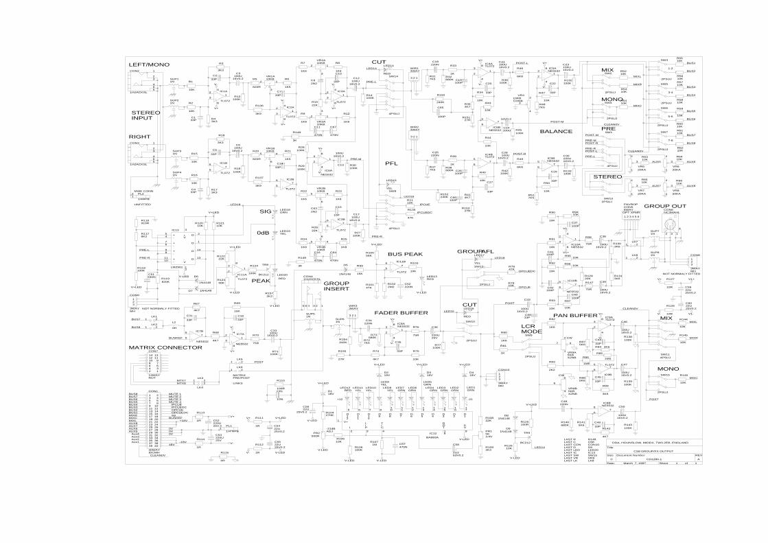
Date: March 7, 1997 Sheet 1 of 1
Size Document Number REV
C CD1280-1 A
Title
CS8 GROUP/FX OUTPUT
DDA, HOUNSLOW, MIDDX, TW3 2EB, ENGLAND.
BUS1
BUS3
BUS4
BUS2
MIXR
MIXL
MIXC
1-2
3-4
R5510K
R5610K
R5710K
R5810K
SW4
2PSUJ
SW5
2PSUJ
SW6
2PSUJ
MIX R5210K
R5310K
R5410K
R132100K
MONO
C23100U16V0.2
SW2
2PSUJ
SW3
2PSUJ
V+
V-
POST-L
R36100K
R46
6K8
R47
10K
R487K5
C21100U16V0.2
3
21
8
4
IC5ANE5532
C22
33P
1
2
3
VR410KBCDNB
V+
V-
R32680K
R33
1K
R34
10K
R354K7
R43
10K
C18220N
C19100P
3
21
8
4
IC4ATL072
R150
240K
C20
33P
R317K5123
WIR13WAY
CUTLED14
RED
LED14
PRE-L
C12100U
16V0.2
SW14
4PSUJ
R14100K
V-
R7
1K6
R8
1K6
R1022K
3
21
8
4IC2A
TL072
3
21
8
4IC3A
TL072
V-
V+
R6
1K5
C7
33P
C10
33PC92N2
1 2
3
VR2A10KB
V-
V+
3
21
8
4IC1A
TL072
C3100U
16V0.2
R13100K
R3
3K3
R136
3K9
R5
820R
C2
33P1 2
3
VR1A10KB
LEFT/MONO
R1
10K
R2
10K
2
1
3
4
56
CON2
1/4JACKSL
SUP11N
SUP21N
RIGHT
2
1
3
4
56
CON3
1/4JACKSL
SUP31N
INPUTSTEREO
R15
10K
C6100U
16V0.2
R43K3
R18
3K3
R20
820R
C5
33P
C133P
4 5
6
VR1B10KB
V+
V+R28100K
C13
100U16V0.2 3
21
8
4
IC6A
NE5532
R21
1K5
C11
470N
C67
470N
1 2
3
VR3A10KB
R148
3K
R9
1K8
123
WIR23WAY
R12
1K8
R39
1K
R44
10K
C25220N
5
67
IC4BTL072
R15127R
C65
100P
BALANCE
POST-R
POST-M
R45100K
C24100U
16V0.2 5
67
IC6BNE5532
POST-M
PRE-M
PRE-L
POST-R
PRE-RPOST-L
PRESW1
4PSUJ
1
2
3
VR520KA
CLEAN0V
CLEAN0V
BUS5
BUS7
BUS8
BUS65-6
7-8
R59
10K
R6010K
R6110K
R6210K
SW7
2PSUJ
1
2
3
VR620KA
GROUP OUT
AUX5 AUX6
AUX7 AUX8
R6410K
R6510K
R6610K
R6310K
1
2
3
VR820KA
STEREOR133100K
C30100U16V0.2
SW132PSUJ
1
2
3
VR720KA
R42100K
R49
6K8
R50
10K
R517K5
C28100U
16V0.2
5
67
IC5BNE5532
C29
33P
IPCUE
R38680K
R40
10K
R414K7
C26100P
R152240K
R15327R
C66100P
C27
33P
R377K5
PFL
LED16
LED15
YEL
PRE-M
R30100K
R1110K
SW8
4PSUJ
LED18GRN
V-
R22
1K6
R23
1K6
R29100K
C15
10P
5
67
IC2B
TL072
C14
33P
C632N2
4 5
6
VR2B10KB
5
67
IC1B
TL072
LED18
R19100K
R173K3
R137
3K9
C433P
SUP41N R16
10K
MWK CONN
UNFITTED
1 2 PL2
1/4RPB
PRE-L
PRE-R
+ 5
- 4 O 2
+ 7
- 6 O 1
+ 9
- 8 O 14
+ 11
- 10 O 13
+V
3
-V
12
IC13
LM2901
R116910R
R1176K2
SIG
0dB
R12010K
R12110K
R12222K
V+LED
V+LED
R2622K
5
67
IC3B
TL072
C16
470NR149
3K
C64
470N
4 5
6
VR3B10KB
LED19YEL
R24
1K8
R25
1K8
BUS PEAK
PRE-R
R27100K
R10056K
R135
47K
C17100U
16V0.2
V+LED
IPCUEDC
AFLLED17
YEL
GROUPLED18
R90
10K
R91
10K
C41100P
R9410K
R9510K
R98
75R
V1-
V1+
C38
100U16V0.2
OPT XFMR
R1303K6
C37
100P
1 2 3 4 5 6
CON56WAY
FHVROP
3
21
8
4
IC10ANE5532
132
4
CON6NC3MAHL
1 2LK7
1 2LK8
SUP71N
SUP81N
123
CON8
3WAYMH
V+ V1+
V1-V-
R127
10R
R128
10R
C5922U25V0.2
C6022U25V0.2
NOT NORMALY FITTED
R9610K
R97
10K
C39
100U16V0.2
R12920K
R1313K6
C40
100P
5
67
IC10B
NE5532
R147
75R
CLEAN0V
OPCUEDC
OPCUE
POST
R92
10K
R93
10K
R7847K
R7910K
C42100P
C43
100U16V0.2
CUTLED16
RED
V-LED
LED13RED
SW12
2PSUJ
D5
1N4148
123
WIR33WAY
R99
15K
R10147K
R1022M2
R103
10K
C62220N
5
67
IC11B
TL072
GROUPINSERT
2 1345 6
CON41/4JACKSL
LED20
RED
V-LED
R1572K2
PEAK
TR8
BC212
R69
10K
R124
100K
3
21
8
4IC11A
TL072
V-LED
R12368K
R67
4K7
R118100K
D6
1N4148
D7 1N4148
V-LED
NOT NORMALY FITTED
123
CON9
3WAYMH
V+LED
C51330N
R119820K
BUSREF
L2
0HBUS8
BUS7 1 2LK1
1 2LK2
MATRIX CONNECTOR
5
67
IC7B
NE5532
C31
33P
12345678910
11121314
CON7
14WAYROT
V+
V-
R68
4K7
R70
75R 3
21
8
4IC7A
NE5532
1 2LK5
C32
33P
R71100K
C33100U
16V0.2
SUP51N
SUP61N
R155
27R
FADER BUFFERV+
V-
R74
4K7
R75
10K
R76
75R
C34220N
3
21
8
4
IC8ANE5532
R73680K
R154240K C35
33P
R727K5
LED16
R77100K
C36
220U25V
SW10
2PSUJ
PAN BUFFER
MODELCR
R80
1K6
R81
1K
R82
1K6
SW9
2PSUJ
C6833P
V+
V-CW
R84 3K6
R875K6
C46
100U16V0.2
3
21
8
4
IC9ATL072
R85
1M5R86
1M5
C44
33P
1
2
3 7
VR9A5KBX2NB
MIXR
MIXLMIX
R138100K
R144
10K
R145
10K
SW114PSUJ
MIXC
POST
MONO
R139100K
R146
10K
SW15
2PSUJ
CWR885K6
R89
3K6
C47
100U16V0.2
C48220N
C50
100U16V0.2
5
67
IC8BNE5532
5
67
IC9B
TL072
C45
33P
4
5
6
VR9B5KBX2NB
V+LED
R83
2K2
123
CON10
3WAYMH
-21
LED1GRN
LED2GRN
LED3GRN
LED4GRN
LED5GRN
V+LED V+LED
D318V
D418V
LED6GRN
LED7GRN
LED12RED
V+LED
D218V
V+ 1
I
2
I/P
3
T/C
4
D12
5
D11
6
D10
7
D9
8
D8
10
D7
11
D6
12
D5
13
D4
14
D3
15
D2
16
D1
17
0V
9
DOT
18IC12
BA683A
LED11YEL
LED10YEL
LED9YEL
LED8YEL
+12
V+LED
R104270K
D118V
R110
100R
C5622U
25V0.2
C61
10N
POST
MATRIXPRE/POST
LINKS 1 2
LK3
1 2
LK4
1 2LK6
BUS2BUS3BUS4BUS5BUS6BUS7BUS8
IPCUEIPCUEDCOPCUE
MTX8MTX7
MUTE 1MUTE 2MUTE 3MUTE 4
1 23 45 67 89 1011 1213 1415 1617 1819 2021 2223 2425 2627 2829 3031 3233 3435 3637 3839 40
CON1
40WAYIDCMH
+18V
0V0V0V
MIXR
MIXL
BUS1
MIXC
AUX5AUX6
BUSREF
-18V
OPCUEDCsip
AUX7AUX8
R113
1R
R114
1R48V
Aux1Aux2Aux3Aux4
CLEAN0V
1 2 PL1
1/4"RPB
V+
V-
V+
V-
R111
1R
R112
1RR115
0R
C52220U25V
C53220U25V
C5422U25V0.2
C5522U25V0.2
-21dBADJ
V-LED
V-LED
R10510K
V+LED
V-LED
PR2500R
V-LEDV-LED
C57470N
R1071M
R106100K
V-LED
R10822K
R1092K2
C58
2U263V0.2
PR15K1/4V
LED14
V-LED
R12610K
R125150R
D81N4148
D91N4148 TR9
BC212LAST RLAST CLAST CONLAST DLAST LEDLAST ICLAST SW
C68
D9
SW15LAST VRLAST LK
R148
LED20
VR9
IC13
LK8
R140680K
R1415K6
R142
4K7
C49
33P
CON10
R143100K

Date: February 27, 1997 Sheet 1 of 2
Size Document Number REV
C CD1281-1 A
Title
CS8 MASTER MODULE.
DDA, HOUNSLOW, MIDDX, TW3 2EB, ENGLAND.
AUX SEND132
4
CON7NC3MAHL
SP71N
123
CON18
3WAYMH
C9
100U16V0.2
R243K6
1 2LK1
1 2 3 4 5 6
CON136WAY
FHV
R1810K
R22
75R 3
21
8
4
IC3ANE5532
C7
220P
R14
10K
R15
10K
V1-
V1+
R8
75R
C5
33P 0.2
C6
100U16V0.2
AUXMTR
AUXINSERT
R7680K
C4220N
3
21
8
4
IC2ATL072
SP21N
V+
V-
1
2
3
VR110KA
R4
10K2 1345 6
CON41/4JACKSL
C2
33P 0.2
AUX1
L1
0H
3
21
8
4 IC1A
NE5532
R2
10K
C1
33P 0.2
AUX1 V-
R3
4K7BUSREF
V+R122R
R5
75R 5
67
IC1B
NE5532
C3
100U16V0.2
SP11N
R6
10K
R10
4K7
AFL
R9
10K
R12
47K
R1310K
LED14
YELSW1
2PSUJ
OPCUEDC
LED15
LED14
R1910K
R2010K
R21
10K
R23
75R
5
67
IC3BNE5532
C8
220P
C64220P
C65220P
R16
10K
R17
10K
R15320K
C10
100U16V0.2
R253K6
1 2LK2
SP81N
NOT NORMALY FITTED
GND
V+
V-
V+
V-
MWKGND
C72
100U16V0.2
LEFTCUT
C19
100U16V0.2
LED22
RED
SW9
2PSUJ
LED23LED22
FADER BUFFER
R38680K
R39
75R
C17220N
3
21
8
4
IC6ANE5532
R124
1K
C38220P
OPCUE
V+
LEFTINSERT
2 1345 6
CON51/4JACKSL
123
WIR13WAY
R1427K5
SP41N
R28
10K
C12
33P 0.2
MIXLEFT
L2
0H
R26
4K7
C11
33P 0.2
MIXL
R27
4K7 3
21
8
4 IC4A
NE5532BUSREF BUSREF
V-
V+
R29
75R 5
67
IC4B
NE5532
SP31N
R301K5
R162
1K5
C13
100U16V0.2
R311K
R160100K
C74
100U16V0.2
LFDR
BUS PEAK
R40
10KR4110K
R42
9K1
R4956K
C18
33P 0.2C20
100U16V0.2
V+
V-
R172
240K
R173
68R
R149100K R150
100K R6210K
3
21
8
4
IC8ANE5532
C25
220P
R58
10K
R59
10K
V1-
V1+
LEFT MIX OUT
R66
75R
C27
100U16V0.2
R683K6
1 2LK3
1 2 3 4 5 6
CON146WAY
FHV
132
4
CON8NC3MAHL
SP91N
123
CON19
3WAYMH
L+R TO C
LED18
GRN
SP101N
SW8
4PSUJ
LED18R67
75R
C28
100U16V0.2
R693K6
LED22
1 2LK4
R6310K
R6410K
R65
10K
5
67
IC8BNE5532
C26
220P
C66220P
C67220P
R60
10K
R61
10K
R15420K
LED13RED
V-
R52
10K
C35220N
3
21
8
4 IC7A
TL072
D11
1N4148
R48
15K
R5047K
R512M2
V-
V+TAPERECORD-10dBV
R371K
C75
100U16V0.2
CON2
DUALPHONO
5
67
IC2BTL072
R361K5
R163
1K5
SP131NREC-C
R169100K
MIXRIGHT R32
4K7
L3
0H
C14
33P 0.2
R34
10K
C15
33P 0.2
INSERTRIGHT
2 1345 6
CON61/4JACKSL
123
WIR23WAY
SP61N
FADER BUFFER
R44
75R
C21220N
5
67
IC6BNE5532
R120
1K
RIGHTCUT
C23
100U16V0.2
LED23
RED
SW10
2PSUJ
LED24LED23
R7410K
C29
220P
C73
100U16V0.2
R70
10K
LPOST
RPOST
1 2 3 4 5 6
CON156WAY
FHV
132
4
CON9NC3MAHL
R8415K
R8515K
LPOST
RPOST
MIXC
SP111N
SP121N
NOT NORMALY FITTED
123
CON20
3WAYMH
R78
75R
C31
100U16V0.2
R803K6
R813K6
1 2LK6
1 2LK5
R7510K
R7610K
3
21
8
4
IC9ANE5532
C68220P
R71
10K
R72
10KR15520K
V1-
V1+
R151100K R152
100K
R43680K
R45
10KR4610K
R47
9K1
C22
33P 0.2C24
100U16V0.2
C39220P
RFDR
V+
R171
240K
R170
68R
R86
100RC37
10N
R1437K5
R161100K
R35
75R 5
67
IC5B
NE5532
D161N4148
C16
100U16V0.2
SP51N
V+ V+
R33
4K7 3
21
8
4 IC5A
NE5532
MIXR
BUSREF
V-
V+
bus1bus2bus3bus4bus5
bus6bus7bus8
MATRIX CONNECTOR
LPOST
RPOSTREC-C
12345678910
11121314
CON16
14WAYROT R87
10K
D171N4148
R11150R
TR17BC212
CPOST
LED14
V-
BUS PEAK
R53
15K
R57
10K
C36220N
5
67
IC7B
TL072
D12
1N4148
R5456K
R5547K
R562M2
R82
10R
R83
10R
C3422U25V0.2
C3322U25V0.2
RPEAK
V+ V1+
V1-V- SEE ALSO CD1282-1
R77
10K
5
67
IC9BNE5532
C30
220P
C69220P
R73
10K
USE WITH PC 1396
RIGHT MIX OUT
LAST RLAST CLAST CONLAST DLAST LEDLAST ICLAST SW
C86
LAST VR VR3
LED24
R197
CON24D21
IC14
LAST TR
SW12
TR21
R79
75R
C32
100U16V0.2

Date: March 6, 1997 Sheet 2 of 2
Size Document Number REV
C CD1282-1 A
Title
CS8 MASTER MODULE.
DDA, HOUNSLOW, MIDDX, TW3 2EB, ENGLAND.
132
4
CON23NC3MAHL
SP151N
R1833K6
C83
100U16V0.2
1 2LK7
1 2 3 4 5 6
CON176WAY
FHV
V1-
V1+
R17610K
R180
75R
C78
100U16V0.2
C81
220P
R188
10K
R189
10K
3
21
8
4
IC15ANE5532
CPOST
LED24
R187100K
CPRE
LED24
RED
CENTRE CUT
V- SW12
2PSUJ
L/RTAPETO
LFDR
RFDR
SW2
2PSUJ
C44
1000U6.3V
R9910K
3
21
8
4IC13A
TL072
R97
22K
R98
47K
V-
V+
C43
33P0.2
1
2
3VR2A10KAX2NB
RPEAK
RTAPELTAPE
LMONRMON
RPEAK
CFDRLEFTCFDRRIGHT
RPOST
METEROFFCPRE
+48VPRECMON
123456789
101112
CON10
12WAYMHR/A
5
67
IC13B
TL072
R100
22K
R90
47KC45
33P0.2
4
5
6VR2B10KAX2NB
CENTRETAPETO
SW3
2PSUJ
C46
1000U6.3V
R10110K
TR18J111
R164
10KR16810K
V-
V+
R165
10KC76
33P
C77
100U16V0.2
3
21
8
4
IC14ATL072
5
67
IC14BTL072
CMON
R174
10K
R175
10K
R17710K
R17810K
R179
10K
R18120K
C79220P
C80220P
C82
220P
5
67
IC15BNE5532 CENTRE MIX OUTR182
75R
C84
100U16V0.2
R1853K6
1 2LK8
SP141N
NOT NORMALY FITTED
123
CON22
3WAYMH
-21
LED1GRN
LED2GRN
V+LED
D418V
LED3GRN
LED4GRN
LED5GRN
LED6GRN
LED7GRN
V+LED V+LED
D218V
D318V
LED9YEL
LED8YEL
+12
LED12RED
V+LED
D118V
LED11YEL
LED10YEL
R106
10K
5
67
IC12BTL072
LMON
C47
33P
C48
100U16V0.2
TR1J111
TR19J111
SW5
2PSUJ
R103
15K
R102
15K
TAPESW6
4PSUJ
CPOST
C TO MON L/RMIXTO
MONSW4
4PSUJ
LINK TO COMMS PCB
LPOST
RPOST
LPOST
RPOST
CPOST CPOST
NOT
FITTED
123456
CON21
6WAYMHLOPT
AUXMTR
NORMALLY
SOLO
R108
4K7
R110
4K7
LEVEL
R104
10K
R105
10K
R166
10KR16710K
1
2
3VR310KBCDNB
MIXDC
TR2J111
-21dBADJ
PR2500R
V+ 1
I
2
I/P
3
T/C
4
D12
5
D11
6
D10
7
D9
8
D8
10
D7
11
D6
12
D5
13
D4
14
D3
15
D2
16
D1
17
0V
9
DOT
18
IC10BA683A
R91270K
R9210K
V-LED
V-LED
C4122U
25V0.2
R93100K LEFT METER
C42470N
R941M
V-LED
1 2 PL1
1/4"RPB
V+
V+
+18VR132
1R C62
220U25V
bus1
bus3bus2
bus4bus5bus6bus7bus8
MIXR
MIXLBUSREFMIXC
OPCUEDC
IPCUEIPCUEDCOPCUE
V-LED
BUSREFSIP
OPCUEOPCUEDC
aux7aux8
MUTE1MUTE2MUTE3MUTE4
1 23 45 67 89 1011 1213 1415 1617 1819 2021 2223 2425 2627 2829 3031 3233 3435 3637 3839 40
CON1
40WAYIDCMH
R962K2
V-LED
PR15K1/4V
TR12J111
TR13J111
C40
2U263V0.2
R95
33K
R134
12K
R107
10K
3
21
8
4
IC12ATL072
RMON
V-
V+
SOLOMTR
LPOSTC49
33P
C50
100U16V0.2
TR3J111
TR4J111
R11310K
R114
10KR11510K
C53
100U16V0.2
R112
10K
R111 33K
3
21
8
4IC11A
NE5532
5
67
IC11BNE5532
V-
V+
SOLOMTR
V+
R135100K
R109
4K7
C51
33P C5233PL4
0HIPCUE
OPCUE
D5
TR6J111
TR21J175
V+
R140100K
C54470N
V-
C86220N
R196
1MR197
68K
D20
D21
V-
R117
100K
SOLOINPLACE
LED15
RED
LED15
INPUT CUE
R116220K
R119
47KIPCUEDC
V+
TR7
BC182
R1184K7
INPUTCUE
LED16YEL
D9
R128100K
SOLODC
V-
C70100N
TR8
BC182
D10
R129100K
METEROFFV-
C71100N
*
1 2
LK9
R144100K
R145100K
D14 D15
MWKGND
R193
1R5
clean0v
aux6
aux4aux3aux2
GND
0V0V0V
+48V
+48V
aux1
aux5
AUX1
D18
+48VPRE
1 2 PL2
1/4"RPB
MWK CONUNFITTED
V-
V-
-18V
R146
27K
R133
1R
C63220U25V
LED19
RED
R186
27K
LED25
GRN
POWER IN
R147
10KR148
10K
LED20
GRNLED21
GRN
123456
CON12
6WAYMH156
+18V
SW11
2PSUJ
R191
2K7
R1922K7
R88
4K7
TR16TIP32CVERT
LITTLITE
*
V-
TR20
ZTX553
C5533U63V
R194
100K
R195
33K
R190100KOPTV+
V-
R12747K
TR11BC182
123
CON11
3WAYMH
* FOR METER BRIDGE OPTIONSREMOVE LK9 AND FIT R190
D7
D8 R126
150K
C5910N
V+
R12510K
R12247K
V-
V-
V+
V+
V+
R136
100KTR14BC212
SW7
2PSUJ
R1374K7
SIP
R138100K
R139
100K
TR15BC182
C85100N
V+ V+LED
V- V-LED
R130
1R
R131
1R
C6022U25V0.2
C6122U25V0.2
OUTPUTCUE
OUTPUT CUE
R121220K
C5810N
OPCUEDC
V-
V-V-
TR9BC182
C572U263V0.2
R123
47K
LED17YEL
LED18
TR10
BC182
-18V +18V
R15722RWW-4W
R15622R
WW-4WEXT METER POWER
NOT NORMALY FITTED
123
CON24
3WAYMH156
LAST RLAST CLAST CONLAST DLAST LEDLAST ICLAST SW
C86
LAST VR
R197
LED25
VR3
IC14
CON24D21
LAST TR
SEE ALSO CD1281-1
-18V
SW12
TR21
USE WITH PC1396-1

Date: February 5, 1997 Sheet 1 of 2
Size Document Number REV
C CD1283-1 A
Title
CS8 COMMS MASTER (CENTRE MIX)
DDA, HOUNSLOW, MIDDX, TW3 2EB, ENGLAND.
132
4
CON7NC3MAHL
SP71N
123
CON22
3WAYMH
C9
100U16V0.2
R243K6
1 2LK2
1 2 3 4 5 6
CON186WAYFHVR18
10K
R22
75R 3
21
8
4
IC3ANE5532
V1-
V1+
C7
220P
R14
10K
R15
10KAFLLED14
YEL
123
CON23
3WAYMH
AUX METER
R8
75R
3
21
8
4
IC2ATL072
V1+
V1- C5
33P
R7680K
C6
100U16V0.2
C4220N
SP21N2 1345 6
CON41/4JACKSL
1
2
3
VR110KA
AUXINSERT
R4
10K
C2
10P
L1
0H
3
21
8
4 IC1A
NE5532
R2
10K
V-AUX2
AUX2C1
10P
R1100K
R3
4K7BUSREF
V+
R5
75R 5
67
IC1B
NE5532
CENTRE
C3
100U16V0.2
SP11N
R6100K
R74
100R
C3810N
2 1345 6
CON51/4JACKSL
R9
10K
R10
4K7
V+LEDR314
5K6
R12
47K
R1310K
OPCUEDC
OPCUE
LED15
SW1
2PSUJ
R1910K
R2010K
R21
10K
R23
75R
5
67
IC3BNE5532
C8
220P
C65220P
C66220P
R16
10K
R17
10K
R22220K
C10
100U16V0.2
R253K6
1 2LK3
AUX 2 SEND
SP81N
R215
100K
R214
330K
R302
100K R303
220K
LED15
RED
LED15
SW2
2PSUJC102470N
R310
100KD225V1
MUTE1
V+
3
2 1
8
4
IC18ANE5532
C19
100U16V0.2
R189100K
CPRE
FADER BUFFER
R38680K
R39
75R
C17220N
3
21
8
4
IC6ANE5532
V+
V-
R36
18K
C18
33PC20
100U16V0.2
R1847K5
123
WIR13WAY
SP41N
SP31N
INSERTR28
10K
R29
75R 5
67
IC4B
NE5532
C13
100U16V0.2
R30100K
REC-C
C12
10P
MIX
L2
0H
R26
4K7
R27
4K7 3
21
8
4 IC4A
NE5532
BUSREF
V-
V+
CENTRE
MIXC
C11
10P
BUS PEAK
CFDRLEFTCFDRRIGHT
5
67
IC2B
TL072
V1+
R3256K
R40
10KR4110K
V+LED
R35
10K
R37
18K R300
240K
123456
CON3
6WAYFHV
R301
68R
MUTE2
V-
5
6 7
IC18BNE5532
LED16
RED
LED17
RED
SW3
2PSUJC103470N
R311
100KD235V1
R218
100KR216
100K
R304
330K
R305
220K
R219
100K
R221
100K
R229
100K
R306
330K
R307
220K
R308
330K
R1175R
LED18
RED
SW5
2PSUJ
SW4
2PSUJC104470N
D205V1
R312
100K
R313
100K
MUTE3
V+
V-
3
2 1
8
4
IC19ANE5532
5
6 7
IC19BNE5532
CPEAK
V-LED
V-
R186100K
D14
1N4148
TR5J111
R31
15K
C24220N
R3347K
R342M2
D5
123456789101112
CON1112WAY
MHR/A
LED13RED
LMONRMON
C16
100U16V0.2
CPRE
CMON
R44
75R
R4610K
TAPE BUFFER
R4347K
R45
9K1
3
21
8
4
IC5ANE5532
CON9DUALPHONO
V1+
V1-C15
33P
C14100U
16V0.2
SP51N
R4747K
R48
75R
R49
9K1
5
67
IC5BNE5532
C22
33P
C21
100U16V0.2
SP61N
V+
V-
RIGHTPEAK
RPOST
R72
10R
METEROFF
C3622U25V0.2
C23
100U16V0.2
V1+ V+ V+LED
V1+
R76
1R C3422U25V0.2
+48VPRE
CPOST
R185100K
V+LED
D218V
V+LED V+LED
D418V
D318V
MUTE4C105470N
D215V1
V-LED
V+V-
R220
100K
R309
220K
-21
LED1GRN
LED2GRN
LED3GRN
LED4GRN
LED5GRN
LED6GRN
+12
LED7GRN
LED12RED
V+ 1
I
2
I/P
3
T/C
4
D12
5
D11
6
D10
7
D9
8
D8
10
D7
11
D6
12
D5
13
D4
14
D3
15
D2
16
D1
17
0V
9
DOT
18
IC9BA683A
LED11YEL
LED10YEL
LED9YEL
LED8YEL
V+LED
V-LED
R53270K
D118V
D151N4148
C2922U
25V0.2
TR6J111
R5133K
V1- V- V-LED
V1-
R77
1R
C3522U25V0.2
V-
V+
R73
10R
C3722U25V0.2
TAPE BUFFER
ipcueipcuedcOPCUE
BUS8BUS7BUS6BUS5BUS4BUS3BUS2
R5010K
MUTE1MUTE2MUTE3MUTE4
1 23 45 67 89 1011 1213 1415 1617 1819 2021 2223 2425 2627 2829 3031 3233 3435 3637 3839 40
CON1
40WAYIDCMH
0V0V0V
BUSREFsip
MIXC
OPCUEDCBUS1MIXRMIXCMIXL
AUX5AUX4AUX3AUX2AUX1
AUX6AUX7AUX8
+48V
MWKGND
AUX2
CLEAN 0V
1 2 PL1
1/4"RPB
+18V
-18V
V+
V-
V-
GND
C32220U25V
C33220U25V
R70
1R
R71
1R
1 2 PL2
1/4RPBMWK CONUNFITTED
bus1bus2bus3bus4bus5
bus6bus7bus8
MATRIX CONNECTOR
CPOSTrpost
lpost
REC-C
12345678910
11121314
CON20
14WAYROT
-21dBADJ
V-LEDR522K2
PR15K
1/4V
PR2500R1/4V
C30
2U250VLP
V-LED
V-LED
R5410K
R561M
R55100K C31
470N
V-LEDRIGHT METER
LAST RLAST CLAST CONLAST DLAST LEDLAST ICLAST SWLAST VR VR4
LED18
CON23
LAST TR
R314
D21
IC19
TR6
SEE ALSO CD1284-1
SW14
C106
USE WITH PC1397-1

Date: March 14, 1997 Sheet 2 of 2
Size Document Number REV
C CD1284-1 A
Title
CS8 COMMS MASTER (TB/MONITOR)
DDA, HOUNSLOW, MIDDX, TW3 2EB, ENGLAND.
132
4
CON15NC3MAHL
SP131NC82
100U16V0.2
V1- LEFT MONITOR
3
21
8
4
IC12ANE5532
R175
10K
R17910K
C80
220P0.2
R224
75R
R166100K
C73100U
16V0.2
MONITORLEFT
5
67
IC11B
TL072
R164
33K
R165100K
C72 10P
0.2
1
3
2
VR4A10KAX3LMON
R163
4K7
C51 10P
0.2
5
67
IC6B
NE5532C52
100U16V0.2
R94100K
R93
150K
R91100K
R9210K
C48100N
C50470N
C4947N
C46
470N
R881K5
R89
1K2
C47
220N
C106
100N
R90330R
R83100K
R8410K
R86
3K3R87
11K
C43470N
C44 10P
0.2
C45470N
5
67
IC7BNE5532
R230100K
R85
150K
V1-
V1+
V+
C402U2
63V0.2
R78
100K
R79
100K
R80
10K
R8110K
C39
2U263V0.2
C4110P0.2
C42 10P
0.2
D169V1
D179V1
3
21
8
4
IC7ANE5532
R82
150K
C53100N
V+
V- R97
18K
R98
6K2
3
21
8
4
IC16A
TL072
R99
10K
R1013K9
R103820R
5
67
IC16B
TL072
C962U2
63V0.2
D18
SW7
4PSUJ
SW6
2PSUJ
OSC ON
CMON
R167
4K7
1
2
3
VR220KA
3
21
8
4 IC11A
TL072
V-
V+
MONITORVOLUME MONITOR
CENTRE
R168
33K
R169100K
C74 10P
0.2
4
6
5
VR4B10KAX3
ONPHONES
R170100K
C75
100U16V0.2
SW14
6PSUJ
V1+
5
67
IC12BNE5532
R176
10K
R177
10K
R18010K
R18110K
R18320K
C78220P0.2
C79220P0.2
C81
220P0.2
R225
75R
SP141N
R1873K6
C83
100U16V0.2
R2263K6
132
4
CON21NC3MAHL
V1- CENTRE MONITOR
R178
10K
R182
10K
R188
10K
R19210K
C86
220P0.2
R174100K
C77
100U16V0.2
MONITOR
R172
33K
R173100K
C76 10P
0.2
5
67
IC10B
TL0727
9
8VR4C
10KAX3
RMON
R171
4K7
OSCILLATOR
R100
10K
R102820R
D19PINK/1KHz
TALKBACK
LINK FOR +48V
MIC
2 3 1
4
CON14NC3FAHR
C54100N
R95150R
R96
9K1
PHANTOM POWER
SP111N
R1046K8
R1056K8
R106
10R
C55680P0.2 D11
9V1R1082K2
R10910K
C57
33U63V0.2
1 2LK1
LK03-OPT+48VPRE
D109V1
TALKBACK
V+R11233R C60
1000U6.3V
C61
100U16V0.2
3
2 6 5
1 8
7
4
IC15
SSM2017
1
2
3
VR310KRD
R114 470R
R115 470R
R116 470R
SW8
4PSUJ
RIGHT
V-
C62 10P
0.2
C63
100U16V0.2
3
21
8
4 IC10A
TL072
R118 47K
R119 47K
R117 4K7
V1+
R19310K
R19410K
R19620K
R197
75R
R198
75R
C84220P0.2
C85220P0.2
3
21
8
4
IC14ANE5532
5
67
IC14BNE5532
R227
10K
R228
10K
R1993K6
R2003K6
C88
100U16V0.2
C89
100U16V0.2
SP171N
SP181N
R191
10K
R195
10K
C87
220P0.2V+
R120100K
TALKBACK
V-
R113100K
C59220P0.2
D139V1
R11010K
R11124K
C58
33U63V0.2
D129V1
SP121N R107
10R
C56680P0.2
AUX1-3
AUX4-6
R121 10K
R122 10K
R123 10K
SW9
2PSUJ
SW10
2PSUJ
AUX1
AUX2
AUX3
SW13
2PSUJ
BUS1
BUS2
BUS3
BUS4
BUS5
BUSR132 10K
R133 10K
R134 10K
R135 10K
R136 10K
R143220K
C98
220N
V2+
V2-
D6
D7
R144680K
R14710K
R14810K
3
21
8
4
IC17A
TL072
C99
33P0.2
V2+
V2-
TR1BC182
TR2BC212
R149
33R
R150
33RR15110K
R152
75RC100
220U 25V
PHONES
123
CON17
3WAYMH
V1-
V1+
RIGHT MONITOR
3
21
8
4
IC13ANE5532
R201
10K
R202
10K
R20510K
R20610K
R210
75R
C90220P0.2
C92
220P0.2
132
4
CON16NC3MAHL
SP151N
R2123K6
C94
100U16V0.2
SP161N
R2133K6
C95
100U16V0.2
5
67
IC13BNE5532
R203
10K
R204
10K
R20710K
R208
10K
R20920K
R211
75RC91
220P0.2
C93
220P0.2
V2+
TR3BC182
TR4BC212
R159
33R
R160
33R
R16110K
R162
75RC71
220U 25VD8
D9
R1453K3
R146
10K
R154680K
R15710K
R15810K
C70
33P0.2
5
67
IC17B
TL072V2+
BUS6
BUS7
BUS8
R137 10K
R138 10K
R139 10K
R153220K
C69
220N
V++48V +48V
AUX4
AUX5
AUX6
AUX7 R140
47R
AUX7-8
R124 10K
R125 10K
R126 10K
R127 10K
SW11
2PSUJ
MIX
R128 10K
R129 10K
R130 10K
R131 10K
SW12
2PSUJ
V+
V-
V+
V-
GND
V1+
V1-
V1+
V1-
V-
MIXL
MIXR
MIXC
AUX8
R141
47R
MWKGND
V2-
R142
0R
C641000U25V
C971000U25V
R1553K3
R156
10K
V2-
SEE ALSO CD1283-1USE WITH PC1397-1
LAST RLAST CLAST CONLAST DLAST LEDLAST ICLAST SWLAST VR VR4
LED18
R314
CON22
IC17
LAST TR
D19
TR6
SW14
C106

Date: January 23, 1996 Sheet 1 of 1
Size Document Number REV
A CD1273-1 & PC1385-1 C
Title
CS3 METER BOARD (CENTRE METER)
DDA, HOUNSLOW, MIDDX, TW3 2EB, ENGLAND.
V+LEDSV+LEDSV+LEDS
V+LEDS
D1S18V
D2S18V
D3S18V
D4S18V
-21
LED1SGRN
LED2SGRN
LED3SGRN
LED4SGRN
LED5SGRN
LED6SGRN
LED7SGRN
LED8SGRN
LED9SRED
LED10SRED
+12
LED11SRED
LED12SRED
V+ 1
I
2
I/P
3
T/C
4
D12
5
D11
6
D10
7
D9
8
D8
10
D7
11
D6
12
D5
13
D4
14
D3
15
D2
16
D1
17
0V
9
DOT
18
IC1SBA683A
V-LEDS
R3S270K
C1S22U
25VLP
-21dBADJ
PR2S500R1/4V R4S
10K
CENTRE METERV-LEDS
V-LEDS
R6S10K C3S
10U16VLP
V-LEDS
R5S47K
V-LEDS
R1S
22K
V-S
V+LEDS
123456
CON1S
6WAYMH12.5
PEAKCENTRE
V-LEDS
V-S
LED13S
RED
R2S2K2
PR1S5K
1/4V
C2S
2U250VLP
METER SUB BOARD

Date: January 23, 1996 Sheet 1 of 1
Size Document Number REV
B CD1271-1 & PC1386-1 C
Title
CS3 PSU BOARD
HOUNSLOW, TW3 2EB INWOOD BUSINESS PARK, HOUNSLOW, MIDDX, TW3 2
KLARK TEKNIK - DDA DIVISION
+48V
D616V
R24
15K
R25
10K
TR4TIP31CVERT
R26
220R
C2333U100V
R1
1R
D3
1N4002
D2
1N4002
D4
1N4002
C1220U100V
D5
1N4002 C3470U100V
C2220U100V
R2
10K
C4100N0.2
TR1ZTX553
R310K
R4
10K
C533U
100V
TR3ZTX453
C24470N
0.2
TR15ZTX553
D722V
PR150K1/4V
R2710K
C733U63V0.2
R23100R
C18100N
EARTH
12345678
CON2
8WAYMETWAY
EARTHEARTH
C25470N
0.2
C34470N0.2
NOT FITTED
R62K2
D13
1N4148
TR2ZTX453
R52K4
NOTFITTED
C610N
0.2
C2633U63V0.2
VoltageDoubler
+18V-18V
AC INAC IN
0V IN
123
CON1
3WAYMETWAY
8 Amp 100VBridge
BR1KBU802
BR2KBU802
C20100N0.2
C19100N
0.2
C21100N0.2
C22100N0.2
R7120R
R80R12.5W/W
TR82N3055-REV
TR7TIP31AVERT
R1010K
R287K5
R124K7
TR5BC212
PR25K1/4V
D816V
C27470N0.2
R13470R
R29
10KTR9BC212
+18V
-18V+18V0V-18V
0V+48V
C12220U25VC28
470N0.2
R30
10K
R112K4
R34
680R
D121N4148
C1110N
R9
680R
TR6BC182
TR16BC182
C101000U40V
C8
100N0.2
C915000U35V
C151000U40V
C13100N C14
15000U35V
C1610N0.2
D10
TR11BC212
TR17BC212
R31
10KR192K4
C32470N0.2
C33470N0.2
R35
680R
C17220U25VC29
470N0.2
R33
10KTR14BC182
PR35K1/4V
D111N4148
TR12TIP32AVERT
R18
10K
R17
680R
TR10BC182
R15120R
R16
0R12.5W/W
TR13MJ2955-REV
R327K5
R204K7
C31
33U 63V0.2
D916V
C30470N0.2
R21470R

Date: February 6, 1997 Sheet 1 of 1
Size Document Number REV
A CD1306-1 A
Title
CS8 BUS LINK
DDA, HOUNSLOW, MIDDX, TW3 2EB, ENGLAND.
Input InputSEND8SEND7SEND6
32A32B31A31B30A30B29A29B28A28B27A27B26A26B25A25B24A24B23A23B22A22B21A21B20A20B19A19B18A18B17A17B16A16B15A15B14A14B13A13B12A12B11A11B10A10B
9A9B8A8B7A7B6A6B5A5B4A4B3A3B2A1A1B
2B
CON3
64WAY-MALE
BUS8BUS7BUS6 Output
IPCUEIPCUEDC
MUTE4MUTE3MUTE2MUTE1BUS8
BUS7BUS6BUS5BUS4BUS3
1 23 45 67 89 1011 1213 1415 1617 1819 2021 2223 2425 2627 2829 3031 3233 3435 3637 3839 40
CON4
40WAYIDCMD
BUS5BUS4BUS3BUS2BUS1MIXRMIXCMIXLAUX8
SEND5SEND4SEND3SEND2SEND1SENDRSENDCSENDLAUXIP8
CUESEND
MUTE1IPMUTE2IPMUTE3IPMUTE4IP
CUEDC
1 23 45 67 89 1011 1213 1415 1617 1819 2021 2223 2425 2627 2829 3031 3233 3435 3637 3839 40
CON2
40WAYIDCMD
SEND8SEND7SEND6SEND5SEND4SEND3
CUESENDCUEDC
MUTE1IPMUTE2IPMUTE3IPMUTE4IP
SEND8SEND7SEND6SEND5SEND4SEND3
1 23 45 67 89 1011 1213 1415 1617 1819 2021 2223 2425 2627 2829 3031 3233 3435 3637 3839 40
CON1
40WAYIDCMD
SEND2SEND1SENDRSENDCSENDLAUXIP8AUXIP7AUXIP6AUXIP5
SEND2SEND1SENDRSENDCSENDLAUXIP8AUXIP7AUXIP6AUXIP5
SIPRECBUSREF
0V0V
+18V+18V+18V
AUXIP7AUXIP6AUXIP5AUXIP4AUXIP3AUXIP2AUXIP1CUESENDCUEDC
SIPRECBUSREF
+18V+18V+18V
0V0V
AUX7AUX6AUX5AUX4AUX3AUX2AUX1
IPCUEIPCUEDC
BUS2BUS1MIXRMIXCMIXLAUX8AUX7AUX6AUX5
SIP
0V0V
+18V+18V+18V
BUSREF
0V
+48V
-18V-18V-18V
AUX4AUX3AUX2AUX1
CLEAN0V
SIP
MUTE3MUTE2MUTE1
0V0V
0V0V
BUSREFSIPRECBUSREF0V0V0V0VMUTE1IPMUTE2IPMUTE3IP
0V-18V-18V-18V+48V
AUXIP4AUXIP3AUXIP2AUXIP1
0V
+48V
-18V-18V-18V
CLEAN0V
AUXIP4AUXIP3AUXIP2AUXIP1CLEAN0V
MUTE4IPMWK
Mounted on trackside of pcb.
MWKMUTE4
MWK CON 1 2 PL1
1/4RPBUNFITTED

Date: February 12, 1997 Sheet 1 of 1
Size Document Number REV
A CD1308-1 A
Title
CS8 BUS LINK BLANKING PLUG
DDA, HOUNSLOW, MIDDX, TW3 2EB, ENGLAND.
BUS8BUS7BUS6BUS5
32A32B31A31B30A30B29A29B28A28B27A27B26A26B25A25B24A24B23A23B22A22B21A21B20A20B19A19B18A18B17A17B16A16B15A15B14A14B13A13B12A12B11A11B10A10B
9A9B8A8B7A7B6A6B5A5B4A4B3A3B2A1A1B
2B
CON1
64WAYDFINV
BUS8BUS7BUS6BUS5BUS4BUS3BUS2BUS1MIXRMIXCMIXLAUX8AUX7
BUS4BUS3BUS2BUS1MIXRMIXCMIXLAUX8AUX7AUX6AUX5AUX4AUX3AUX2AUX1
IPCUE
SIPIPCUEDC
AUX6AUX5AUX4AUX3AUX2AUX1
IPCUEIPCUEDC
SIP
MUTE4MUTE3MUTE2MUTE1
0V0V
0V0V
BUS_REF BUS_REF
MUTE4MUTE3MUTE2MUTE1
0V0V
0V0V
MWKMWK

Date: March 6, 1997 Sheet 1 of 1
Size Document Number REV
D CD1307-1 A
Title
CS8 INPUT METER PCB
DDA, HOUNSLOW, MIDDX, TW3 2EB, ENGLAND.
V+
R1722K
D11N41480.4"
D21N41480.4"
V+
-21
V-
+ 5
- 4 O 2
+ 7
- 6 O 1
+ 9
- 8 O 14
+ 11
- 10 O 13
+V
3
-V
12
IC1LM2901
LED1GRN
LED2GRN
R18120R
R475R
R3270R V+
-21
V+ V+
LED13GRN
LED14GRN
R19120R
+ 5
- 4 O 2
+ 7
- 6 O 1
+ 9
- 8 O 14
+ 11
- 10 O 13
+V
3
-V
12
IC4LM2901
TR1
BC212AI
TR2
BC212AI
V+
-21
V+
LED25GRN
LED26GRN
R20120R
+ 5
- 4 O 2
+ 7
- 6 O 1
+ 9
- 8 O 14
+ 11
- 10 O 13
+V
3
-V
12
IC7LM2901
TR3
BC212AI
V+
-21
V+
LED37GRN
LED38GRN
R21120R
+ 5
- 4 O 2
+ 7
- 6 O 1
+ 9
- 8 O 14
+ 11
- 10 O 13
+V
3
-V
12
IC10LM2901
TR4
BC212AI
V+
-21
V+
LED49GRN
LED50GRN
R22120R
+ 5
- 4 O 2
+ 7
- 6 O 1
+ 9
- 8 O 14
+ 11
- 10 O 13
+V
3
-V
12
IC13LM2901
TR5
BC212AI
V+
-21 -21
V+
LED61GRN
LED62GRN
R23120R
+ 5
- 4 O 2
+ 7
- 6 O 1
+ 9
- 8 O 14
+ 11
- 10 O 13
+V
3
-V
12
1C16LM2901
TR6
BC212AI
V+
-21
V+
LED73GRN
LED74GRN
R24120R
+ 5
- 4 O 2
+ 7
- 6 O 1
+ 9
- 8 O 14
+ 11
- 10 O 13
+V
3
-V
12
IC19LM2901
TR7
BC212AI
V+
V+
LED85GRN
LED86GRN
R25120R
+ 5
- 4 O 2
+ 7
- 6 O 1
+ 9
- 8 O 14
+ 11
- 10 O 13
+V
3
-V
12
IC22LM2901
TR8
BC212AI
V-
V+
LED87GRN
LED88GRN
LED89GRN
V-
V+
-18
-15
-12
-9
LED75GRN
LED76GRN
LED77GRN
V-
V+
-18 -18
-15 -15
-12 -12
-9 -9
LED63GRN
LED64GRN
LED65GRN
V-
V+
-18
-15
-12
-9
LED51GRN
LED52GRN
LED53GRN
V-
V+
-18
-15
-12
-9
LED39GRN
LED40GRN
LED41GRN
V-
V+
-18
-15
-12
-9
LED27GRN
LED28GRN
LED29GRN
V-
V+
-18
-15
-12
-9
LED15GRN
LED16GRN
LED17GRN
V-
V+
LED4GRN
-18
-15
-12
-9
LED3GRN
LED5GRN
R6120R
R7180R
R8270R
V-
-6
-3
0
LED6GRN
LED7GRN
+ 5
- 4 O 2
+ 7
- 6 O 1
+ 9
- 8 O 14
+ 11
- 10 O 13
+V
3
-V
12
IC2LM2901
R9360R
R10510R
R121K
R11820R
LED8YEL
V-
-6
-3
0
LED18GRN
LED19GRN
+ 5
- 4 O 2
+ 7
- 6 O 1
+ 9
- 8 O 14
+ 11
- 10 O 13
+V
3
-V
12
IC5LM2901
LED20YEL
V-
-6
-3
0
LED30GRN
LED31GRN
+ 5
- 4 O 2
+ 7
- 6 O 1
+ 9
- 8 O 14
+ 11
- 10 O 13
+V
3
-V
12
IC8LM2901
LED32YEL
V-
-6
-3
0
LED42GRN
LED43GRN
+ 5
- 4 O 2
+ 7
- 6 O 1
+ 9
- 8 O 14
+ 11
- 10 O 13
+V
3
-V
12
IC11LM2901
LED44YEL
V-
-6
-3
0
LED54GRN
LED55GRN
+ 5
- 4 O 2
+ 7
- 6 O 1
+ 9
- 8 O 14
+ 11
- 10 O 13
+V
3
-V
12
IC14LM2901
LED56YEL
V-
-6 -6
-3 -3
0
LED66GRN
LED67GRN
+ 5
- 4 O 2
+ 7
- 6 O 1
+ 9
- 8 O 14
+ 11
- 10 O 13
+V
3
-V
12
IC17LM2901
LED68YEL
V-
-6
-3
0 0
LED78GRN
LED79GRN
+ 5
- 4 O 2
+ 7
- 6 O 1
+ 9
- 8 O 14
+ 11
- 10 O 13
+V
3
-V
12
IC20LM2901
LED80YEL
V-
LED90GRN
LED91GRN
+ 5
- 4 O 2
+ 7
- 6 O 1
+ 9
- 8 O 14
+ 11
- 10 O 13
+V
3
-V
12
IC23LM2901
LED92YEL
V-
V+
+ 5
- 4 O 2
+ 7
- 6 O 1
+ 9
- 8 O 14
+ 11
- 10 O 13
+V
3
-V
12
IC24LM2901
LED93YEL
LED94YEL
LED95YEL
V-
V+
+3
+6 +6
+9 +9
+ 5
- 4 O 2
+ 7
- 6 O 1
+ 9
- 8 O 14
+ 11
- 10 O 13
+V
3
-V
12
IC21LM2901
LED81YEL
LED82YEL
LED83YEL
V-
V+
+3 +3
+6
+9
+ 5
- 4 O 2
+ 7
- 6 O 1
+ 9
- 8 O 14
+ 11
- 10 O 13
+V
3
-V
12
IC18LM2901
LED69YEL
LED70YEL
LED71YEL
V-
V+
+3
+6
+9
+ 5
- 4 O 2
+ 7
- 6 O 1
+ 9
- 8 O 14
+ 11
- 10 O 13
+V
3
-V
12
IC15LM2901
LED57YEL
LED58YEL
LED59YEL
V-
V+
+3
+6
+9
+ 5
- 4 O 2
+ 7
- 6 O 1
+ 9
- 8 O 14
+ 11
- 10 O 13
+V
3
-V
12
IC12LM2901
LED47YEL
LED46YEL
LED45YEL
V-
V+
+3
+6
+9
+ 5
- 4 O 2
+ 7
- 6 O 1
+ 9
- 8 O 14
+ 11
- 10 O 13
+V
3
-V
12
IC9LM2901
LED35YEL
LED34YEL
LED33YEL
V-
V+
+ 5
- 4 O 2
+ 7
- 6 O 1
+ 9
- 8 O 14
+ 11
- 10 O 13
+V
3
-V
12
IC6LM2901
+3
+6
+9
LED21YEL
LED22YEL
LED23YEL
V-
V+
+3
+6
+9
+ 5
- 4 O 2
+ 7
- 6 O 1
+ 9
- 8 O 14
+ 11
- 10 O 13
+V
3
-V
12
IC3LM2901
R131K5
R142K
R153K
LED11YEL
LED10YEL
LED9YEL
V+
+12
LED12RED
R1624K
V- V-
+12
LED24RED
V-
+12
LED36RED
V-
+12
LED48RED
V-
+12
LED60RED
V-
+12
LED72RED
V-
+12 +12
LED84RED
V-
LED96RED
METER-5
METER-6
METER-7
V+
V-
3
21
4
11
IC26A
TL074
5
67
IC26BTL074
10
98
IC26CTL074
V+
V-
3
21
4
11
IC25A
TL074
5
67
IC25BTL074
123456789
1011121314
CON1
14WAYIDCMD
V+
R110R
METER-5METER-6METER-7METER-8
C1
220U25V
C2
220U25V
V-
R210R
R344M7
C3220N
C4220N
10
98
IC25CTL074
12
1314
IC25DTL074R35
4M7R364M7
R374M7
C5220N
C6220N
R414M7
R384M7
R394M7
R404M7
C7220N
C8220N
C9220N
C10220N
METER-8 12
1314
IC26DTL074
LAST CLAST CONLAST DLAST LEDLAST IC
CON1
LAST R R41
D2LED96IC26
C10
This draw
ing is split across the following tw
o pages to aid readability.

Date: May 1, 1997 Sheet 1 of 2
Size Document Number REV
C CD1307-1 A
Title
CS8 - INPUT METER
Klark Teknik - DDA Division
CURRENT REF
V+
R1722K
D11N41480.4"
D21N41480.4"
V-
R3270R
V+
R18120R
TR1
BC212AI
V+
R19120R
TR2
BC212AI
V+
R20120R
TR3
BC212AI
V+
R21120R
TR4
BC212AI
V+LED37GRN
LED38GRN
LED39GRN
-21
-18
-15
LED25GRN
LED26GRN
LED27GRN
+ 5
- 4 O 2
+ 7
- 6 O 1
+ 9
- 8 O 14
+ 11
- 10 O 13
+V
3
-V
12
IC10LM2901
V+
-21
-18
-15
+ 5
- 4 O 2
+ 7
- 6 O 1
+ 9
- 8 O 14
+ 11
- 10 O 13
+V
3
-V
12
IC7LM2901
V+LED13GRN
LED14GRN
LED15GRN
+ 5
- 4 O 2
+ 7
- 6 O 1
+ 9
- 8 O 14
+ 11
- 10 O 13
+V
3
-V
12
IC4LM2901
V+
-21
-18
-15
LED1GRN
LED2GRN
LED3GRN
-21
-18
-15
+ 5
- 4 O 2
+ 7
- 6 O 1
+ 9
- 8 O 14
+ 11
- 10 O 13
+V
3
-V
12
IC1LM2901
R6120R
R475R
-12
-9
R7180R
R8270R
V-
V+
LED4GRN
-12
-9LED5GRN
V-
V+
LED16GRN
LED17GRN
V-
V+
-12
-9
-12
-9
LED28GRN
LED29GRN
V-
V+
LED40GRN
LED41GRN
V+
3
21
4
11
IC25A
TL074
V-
R364M7
R374M7
C6220N
5
67
IC25BTL074
10
98
IC25CTL074
12
1314
IC25DTL074
R344M7
R354M7
C3220N
C4220N
C5220N
V-
123456789
1011121314
CON1
14WAYIDCMD
METER-5METER-6METER-7METER-8
LED42
GRN
LED43GRN
-6
-3
LED30GRN
LED31GRN
+ 5
- 4 O 2
+ 7
- 6 O 1
+ 9
- 8 O 14
+ 11
- 10 O 13
+V
3
-V
12
IC11LM2901
V-
-6
-3
+ 5
- 4 O 2
+ 7
- 6 O 1
+ 9
- 8 O 14
+ 11
- 10 O 13
+V
3
-V
12
IC8LM2901
V-
LED18GRN
LED19GRN
+ 5
- 4 O 2
+ 7
- 6 O 1
+ 9
- 8 O 14
+ 11
- 10 O 13
+V
3
-V
12
IC5LM2901
V-
-6
-3
LED6GRN
LED7GRN
-6
-3
+ 5
- 4 O 2
+ 7
- 6 O 1
+ 9
- 8 O 14
+ 11
- 10 O 13
+V
3
-V
12
IC2LM2901
R9360R
R10510R
R11820R
0
+3
+ 5
- 4 O 2
+ 7
- 6 O 1
+ 9
- 8 O 14
+ 11
- 10 O 13
+V
3
-V
12
IC3LM2901
R121K
R131K5
V+
0
+3
LED10YEL
LED9YEL
LED8YEL
V+
+ 5
- 4 O 2
+ 7
- 6 O 1
+ 9
- 8 O 14
+ 11
- 10 O 13
+V
3
-V
12
IC6LM2901
LED20YEL
LED21YEL
LED22YEL
V+
0
+3
+ 5
- 4 O 2
+ 7
- 6 O 1
+ 9
- 8 O 14
+ 11
- 10 O 13
+V
3
-V
12
IC9LM2901
0
+3
+ 5
- 4 O 2
+ 7
- 6 O 1
+ 9
- 8 O 14
+ 11
- 10 O 13
+V
3
-V
12
IC12LM2901
LED34YEL
LED33YEL
LED32YEL
V+V+
R110R
LED46YEL
LED45YEL
LED44YEL
C1
220U25V
C2
220U25V
V-
R210R
V-
LED48RED
LED47YEL
+6
+9
+12
LED36RED
LED35YEL
V-
+6
+9
+12
V-
LED24RED
LED23YEL
V-
+6
+9
+12
LED12RED
LED11YEL
+6
+9
+12
R142K
R153K
R1624K
V+V- V- V- V-

Date: May 1, 1997 Sheet 2 of 2
Size Document Number REV
C CD1307-1 A
Title
CS8 - INPUT METER
Klark Teknik - DDA Division
V+
R25120R
V+
R24120R
V+
R23120R
V+
R22120R
CURRENT REF
V+
-21
+ 5
- 4 O 2
+ 7
- 6 O 1
+ 9
- 8 O 14
+ 11
- 10 O 13
+V
3
-V
12
IC13LM2901
-21LED49GRN
+ 5
- 4 O 2
+ 7
- 6 O 1
+ 9
- 8 O 14
+ 11
- 10 O 13
+V
3
-V
12
1C16LM2901
TR5
BC212AI
V+
-21LED61GRN
TR6
BC212AI
V+LED73GRN
+ 5
- 4 O 2
+ 7
- 6 O 1
+ 9
- 8 O 14
+ 11
- 10 O 13
+V
3
-V
12
IC19LM2901
TR7
BC212AI
V+
-21
+ 5
- 4 O 2
+ 7
- 6 O 1
+ 9
- 8 O 14
+ 11
- 10 O 13
+V
3
-V
12
IC22LM2901
LED85GRN
TR8
BC212AI
LED86GRN
LED87GRN
LED88GRN
V-
-18
-15
-12
V-
LED74GRN
LED75GRN
LED76GRN
V-
-18
-15
-12
LED62GRN
LED63GRN
LED64GRN
-18
-15
-12
LED50GRN
LED51GRN
LED52GRN
V-
-18
-15
-12
METER-5
V+
3
21
4
11
IC26A
TL074
V+
-9
-6
+ 5
- 4 O 2
+ 7
- 6 O 1
+ 9
- 8 O 14
+ 11
- 10 O 13
+V
3
-V
12
IC14LM2901
-9
-6
LED53GRN
LED54GRN
+ 5
- 4 O 2
+ 7
- 6 O 1
+ 9
- 8 O 14
+ 11
- 10 O 13
+V
3
-V
12
IC17LM2901
V+
-9
-6
LED65GRN
LED66GRN
V+LED77GRN
LED78GRN
+ 5
- 4 O 2
+ 7
- 6 O 1
+ 9
- 8 O 14
+ 11
- 10 O 13
+V
3
-V
12
IC20LM2901
V+
-9
-6
+ 5
- 4 O 2
+ 7
- 6 O 1
+ 9
- 8 O 14
+ 11
- 10 O 13
+V
3
-V
12
IC23LM2901
LED89GRN
LED90GRN
LED91GRN
LED92YEL
V-
-3
0
V-
LED79GRN
LED80YEL
V-
-3
0
LED67GRN
LED68YEL
-3
0
LED55GRN
LED56YEL
V-
-3
0
METER-6
METER-7
METER-8
V- 5
67
IC26BTL074
10
98
IC26CTL074
12
1314
IC26DTL074
R414M7
R384M7
R394M7
R404M7
C7220N
C8220N
C9220N
C10220N V+
+3
+6
+9
+ 5
- 4 O 2
+ 7
- 6 O 1
+ 9
- 8 O 14
+ 11
- 10 O 13
+V
3
-V
12
IC15LM2901
+3
+6
+9
+ 5
- 4 O 2
+ 7
- 6 O 1
+ 9
- 8 O 14
+ 11
- 10 O 13
+V
3
-V
12
IC18LM2901
LED57YEL
LED58YEL
LED59YEL
V+
+3
+6
+9
LED69YEL
LED70YEL
LED71YEL
V+
+ 5
- 4 O 2
+ 7
- 6 O 1
+ 9
- 8 O 14
+ 11
- 10 O 13
+V
3
-V
12
IC21LM2901
LED81YEL
LED82YEL
LED83YEL
V+
+3
+6
+9
+ 5
- 4 O 2
+ 7
- 6 O 1
+ 9
- 8 O 14
+ 11
- 10 O 13
+V
3
-V
12
IC24LM2901
LED93YEL
LED94YEL
LED95YEL
V-
LED96RED
V-
+12
V-
V-
LED84RED
V-
V-
+12
LED72RED
V-
+12
LED60RED
V-
+12

Date: March 21, 1997 Sheet 1 of 1
Size Document Number REV
D CD1311-1 A
Title
CS8 LED OUTPUT METER PCB
DDA, HOUNSLOW, MIDDX, TW3 2EB, ENGLAND.
V+
V+
LED85GRN
LED86GRN
+ 5
- 4 O 2
+ 7
- 6 O 1
+ 9
- 8 O 14
+ 11
- 10 O 13
+V
3
-V
12
IC22LM2901
TR8
BC212AI
R25
120R
V+
-21
-18
V+ V+
LED73GRN
LED74GRN
+ 5
- 4 O 2
+ 7
- 6 O 1
+ 9
- 8 O 14
+ 11
- 10 O 13
+V
3
-V
12
IC19LM2901
TR7
BC212AI
R24
120R
V+
-21 -21
-18 -18
V+
LED61GRN
LED62GRN
TR6
BC212AI
R23
120R
+ 5
- 4 O 2
+ 7
- 6 O 1
+ 9
- 8 O 14
+ 11
- 10 O 13
+V
3
-V
12
IC16LM2901
V+
-21
-18
V+
LED49GRN
LED50GRN
+ 5
- 4 O 2
+ 7
- 6 O 1
+ 9
- 8 O 14
+ 11
- 10 O 13
+V
3
-V
12
IC13LM2901
TR5
BC212AI
R22
120R
V+
-21
-18
V+
LED37GRN
LED38GRN
+ 5
- 4 O 2
+ 7
- 6 O 1
+ 9
- 8 O 14
+ 11
- 10 O 13
+V
3
-V
12
IC10LM2901
TR4
BC212AI
R20
120R
R21
120R
V+
-21
-18
V+
LED25GRN
LED26GRN
+ 5
- 4 O 2
+ 7
- 6 O 1
+ 9
- 8 O 14
+ 11
- 10 O 13
+V
3
-V
12
IC7LM2901
TR3
BC212AI
R19
120R
V+
-21
-18
V+
LED13GRN
LED14GRN
+ 5
- 4 O 2
+ 7
- 6 O 1
+ 9
- 8 O 14
+ 11
- 10 O 13
+V
3
-V
12
IC4LM2901
TR1
BC212AI
TR2
BC212AI
R18
120R
V+
-21
-18
V-
V+
+ 5
- 4 O 2
+ 7
- 6 O 1
+ 9
- 8 O 14
+ 11
- 10 O 13
+V
3
-V
12
IC1LM2901
LED1GRN
LED2GRN
R6120R
D2
1N41480.4"
D1
1N41480.4"R17
22K
BASEREF
R3270R
R475R
V-
V+
LED4GRN
-15
-12
-9
-6
LED3GRN
LED5GRN
LED6GRN
+ 5
- 4 O 2
+ 7
- 6 O 1
+ 9
- 8 O 14
+ 11
- 10 O 13
+V
3
-V
12
IC2LM2901
R7180R
R8270R
R9360R
R10510R
V-
V+
-15
-12
-9
-6
LED15GRN
LED16GRN
LED17GRN
LED18GRN
+ 5
- 4 O 2
+ 7
- 6 O 1
+ 9
- 8 O 14
+ 11
- 10 O 13
+V
3
-V
12
IC5LM2901
V-
V+
-15
-12
-9
-6
LED27GRN
LED28GRN
LED29GRN
LED30GRN
+ 5
- 4 O 2
+ 7
- 6 O 1
+ 9
- 8 O 14
+ 11
- 10 O 13
+V
3
-V
12
IC8LM2901
V-
V+
-15
-12
-9
-6
LED39GRN
LED40GRN
LED41GRN
LED42GRN
+ 5
- 4 O 2
+ 7
- 6 O 1
+ 9
- 8 O 14
+ 11
- 10 O 13
+V
3
-V
12
IC11LM2901
V-
V+
-15
-12
-9
-6
LED51GRN
LED52GRN
LED53GRN
LED54GRN
+ 5
- 4 O 2
+ 7
- 6 O 1
+ 9
- 8 O 14
+ 11
- 10 O 13
+V
3
-V
12
IC14LM2901
V-
V+
-15 -15
-12 -12
-9 -9
-6 -6
LED63GRN
LED64GRN
LED65GRN
LED66GRN
+ 5
- 4 O 2
+ 7
- 6 O 1
+ 9
- 8 O 14
+ 11
- 10 O 13
+V
3
-V
12
IC17LM2901
V-
V+
-15
-12
-9
-6
LED75GRN
LED76GRN
LED77GRN
LED78GRN
+ 5
- 4 O 2
+ 7
- 6 O 1
+ 9
- 8 O 14
+ 11
- 10 O 13
+V
3
-V
12
IC20LM2901
V-
V+
LED87GRN
LED88GRN
LED89GRN
LED90GRN
+ 5
- 4 O 2
+ 7
- 6 O 1
+ 9
- 8 O 14
+ 11
- 10 O 13
+V
3
-V
12
IC23LM2901
V-
V+
LED91GRN
+ 5
- 4 O 2
+ 7
- 6 O 1
+ 9
- 8 O 14
+ 11
- 10 O 13
+V
3
-V
12
IC24LM2901
LED92YEL
LED93YEL
V-
V+
-3
0 0
+3
LED79GRN
+ 5
- 4 O 2
+ 7
- 6 O 1
+ 9
- 8 O 14
+ 11
- 10 O 13
+V
3
-V
12
IC21LM2901
LED80YEL
LED81YEL
V-
V+
-3 -3
0
+3 +3
LED67GRN
+ 5
- 4 O 2
+ 7
- 6 O 1
+ 9
- 8 O 14
+ 11
- 10 O 13
+V
3
-V
12
IC18LM2901
LED68YEL
LED69YEL
V-
V+
-3
0
+3
LED55GRN
+ 5
- 4 O 2
+ 7
- 6 O 1
+ 9
- 8 O 14
+ 11
- 10 O 13
+V
3
-V
12
IC15LM2901
LED56YEL
LED57YEL
V-
V+
-3
0
+3
LED43GRN
+ 5
- 4 O 2
+ 7
- 6 O 1
+ 9
- 8 O 14
+ 11
- 10 O 13
+V
3
-V
12
IC12LM2901
LED44YEL
LED45YEL
V-
V+
-3
0
+3
LED31GRN
+ 5
- 4 O 2
+ 7
- 6 O 1
+ 9
- 8 O 14
+ 11
- 10 O 13
+V
3
-V
12
IC9LM2901
LED32YEL
LED33YEL
V-
V+
+ 5
- 4 O 2
+ 7
- 6 O 1
+ 9
- 8 O 14
+ 11
- 10 O 13
+V
3
-V
12
IC6LM2901
-3
0
+3
LED19GRN
LED20YEL
LED21YEL
V-
V+
-3
0
+3
LED7GRN
+ 5
- 4 O 2
+ 7
- 6 O 1
+ 9
- 8 O 14
+ 11
- 10 O 13
+V
3
-V
12
IC3LM2901
R121K
R131K5
R11820R
LED8YEL
LED9YEL
V-
V+
+6
+9
+12
LED12RED
R142K
R153K
METER1
LED10YEL
LED11YEL
R1630K
V-
V-
V-
+6
+9
+12
LED24RED
METER2
LED22YEL
LED23YEL
V-
V-
+6
+9
+12
LED36RED
METER3
LED34YEL
LED35YEL
V-
V-
+6
+9
+12
LED48RED
METER4
LED46YEL
LED47YEL
V-
V-
+6
+9
+12
LED60RED
METER5
LED58YEL
LED59YEL
V-
V-
+6
+9
+12
LED72RED
METER6
LED70YEL
LED71YEL
V-
V-
+6 +6
+9 +9
+12 +12
LED84RED
METER7
LED82YEL
LED83YEL
V-
V-
LED96RED
METER8
LED94YEL
LED95YEL
GRPSWAUXSWMATSWRECTRGRPLEDAUXLEDMATLED
12345678910
CON1
10WAYFHV
12
CON4S
2WAYWIR
12
CON4
2WAYML
GROUPSW1
TP2301
V+
R37
10K
C147NV+S
PART OF SUB PCB
12
CON3S
2WAYWIR
12
CON3
2WAYML
V+
V+
-21
-18
V+
+ 5
- 4 O 2
+ 7
- 6 O 1
+ 9
- 8 O 14
+ 11
- 10 O 13
+V
3
-V
12
IC31LM2901
LED121GRN
LED122GRN
R28
120RTR11
BC212AI
V+
-21
-18
V+
+ 5
- 4 O 2
+ 7
- 6 O 1
+ 9
- 8 O 14
+ 11
- 10 O 13
+V
3
-V
12
IC28LM2901
LED109GRN
LED110GRN
R27
120RTR10
BC212AI
V+
-21
-18
LED97GRN
LED98GRN
+ 5
- 4 O 2
+ 7
- 6 O 1
+ 9
- 8 O 14
+ 11
- 10 O 13
+V
3
-V
12
IC25LM2901
R26
120RTR9
BC212AI
BASEREF
V-
V+
-15
-12
-9
-6
LED99GRN
LED100GRN
LED101GRN
LED102GRN
+ 5
- 4 O 2
+ 7
- 6 O 1
+ 9
- 8 O 14
+ 11
- 10 O 13
+V
3
-V
12
IC26LM2901
V-
V+
-15
-12
-9
-6
+ 5
- 4 O 2
+ 7
- 6 O 1
+ 9
- 8 O 14
+ 11
- 10 O 13
+V
3
-V
12
IC29LM2901
LED111GRN
LED112GRN
LED113GRN
LED114GRN
V-
V+
-15
-12
-9
-6
+ 5
- 4 O 2
+ 7
- 6 O 1
+ 9
- 8 O 14
+ 11
- 10 O 13
+V
3
-V
12
IC32LM2901
LED123GRN
LED124GRN
LED125GRN
LED126GRN
METER1METER2METER3METER4METER5METER6METER7METER8RECTLRECTC
12345678910
CON2
10WAYFHV
AUX
SW2
TP2301
SW3
TP2301
VSS VSS
V+
C247N
R29
1K
R30100K
R31
1K
12
CON5S
2WAYWIR
12
CON5
2WAYML
V-
VSS
V+S
PART OF SUB PCB
12
CON6S
2WAYWIR
12
CON6
2WAYML
2 4 6 8 10 12 14 16
13579111315
LED135
LEDBLK-REDR342K2
D36V80.4"
R39360R MATRIX LED
AUX LED
GROUP LED
V+S
2 4 6 8 10 12 14 16
13579111315
LED134
LEDBLK-RED
2 4 6 8 10 12 14 16
13579111315
LED133
LEDBLK-RED
R352K2
VSSVSS
C347N
R33100K
MATRIX
R3810K
V-
V+
-3
0
+3
+ 5
- 4 O 2
+ 7
- 6 O 1
+ 9
- 8 O 14
+ 11
- 10 O 13
+V
3
-V
12
IC33LM2901
LED127GRN
LED128YEL
LED129YEL
V-
V+
-3
0
+3
+ 5
- 4 O 2
+ 7
- 6 O 1
+ 9
- 8 O 14
+ 11
- 10 O 13
+V
3
-V
12
IC30LM2901
LED115GRN
LED116YEL
LED117YEL
V-
V+
-3
0
+3
LED103GRN
+ 5
- 4 O 2
+ 7
- 6 O 1
+ 9
- 8 O 14
+ 11
- 10 O 13
+V
3
-V
12
IC27LM2901
LED104YEL
LED105YEL
V-
V-
+6
+9
+12RECTL
LED108RED
LED106YEL
LED107YEL
V-
V-
+6
+9
+12RECTC
LED120RED
LED118YEL
LED119YEL
V-
V-
+6
+9
+12RECTR
LED132RED
LED130YEL
LED131YEL
LAST CLAST CONLAST DLAST LEDLAST IC
CON7
LAST R
IC33LED135
LAST TR TR11LAST SW SW3
V-
R51C3
D5
12
CON7S
2WAYWIR
12
CON7
2WAYML
R362K2
This draw
ing is split across the following three pages to aid readability.

Date: May 2, 1997 Sheet 1 of 3
Size Document Number REV
C CD1311-1 A
Title
CS8 - LED OUTPUT MAIN
Klark Teknik - DDA Division
GRPSWAUXSWMATSW
12345678910
CON1
10WAYFHV
GROUPSW1
TP2301
C147N
12
CON4S
2WAYWIR
12
CON4
2WAYML
V+R28
120R
V+
R37
10K
V+S
PART OF SUB PCB
12
CON3S
2WAYWIR
12
CON3
2WAYML
V+
+ 5
- 4 O 2
+ 7
- 6 O 1
+ 9
- 8 O 14
+ 11
- 10 O 13
+V
3
-V
12
IC31LM2901
LED121GRN
TR11
BC212AI
V+
-21
V+
+ 5
- 4 O 2
+ 7
- 6 O 1
+ 9
- 8 O 14
+ 11
- 10 O 13
+V
3
-V
12
IC28LM2901
LED109GRN
R27
120RTR10
BC212AI
-21
V+
LED97GRN
R26
120RTR9
BC212AI
V+
-21
+ 5
- 4 O 2
+ 7
- 6 O 1
+ 9
- 8 O 14
+ 11
- 10 O 13
+V
3
-V
12
IC25LM2901
CURRENT REF
V-
-18
-15
-12
-18
-15
-12
LED98GRN
LED99GRN
V-
-18
-15
-12
LED110GRN
LED111GRN
V-
LED122GRN
LED123GRN
AUX
SW3
TP2301
VSS VSS
V+
C247N
R29
1K
R30100K
RECTRGRPLEDAUXLEDMATLED
VSS
D36V80.4"
V-
12
CON6
2WAYML
R39360R
C347N
R31
1K
R33100K
MATRIX
SW2
TP230112
CON5S
2WAYWIR
12
CON5
2WAYML
R3810K
V+
+ 5
- 4 O 2
+ 7
- 6 O 1
+ 9
- 8 O 14
+ 11
- 10 O 13
+V
3
-V
12
IC32LM2901
LED124GRN
LED125GRN
LED126GRN
V+
-9
-6
+ 5
- 4 O 2
+ 7
- 6 O 1
+ 9
- 8 O 14
+ 11
- 10 O 13
+V
3
-V
12
IC29LM2901
LED112GRN
LED113GRN
LED114GRN
-9
-6
LED100GRN
LED101GRN
LED102GRN
V+
-9
-6
+ 5
- 4 O 2
+ 7
- 6 O 1
+ 9
- 8 O 14
+ 11
- 10 O 13
+V
3
-V
12
IC26LM2901
V-
-3
0
-3
0
LED103GRN
LED104YEL
V-
-3
0
LED115GRN
LED116YEL
V-
LED127GRN
LED128YEL
V+S
PART OF SUB PCB
2 4 6 8 10 12 14 16
13579111315
LED135
LEDBLK-RED
METER1METER2METER3METER4METER5METER6
VSSVSS
12345678910
CON2
10WAYFHV
V-
12
CON7
2WAYML
MATRIX LED METER7METER8RECTLRECTC
V+S
12
CON6S
2WAYWIR
2 4 6 8 10 12 14 16
13579111315
LED134
LEDBLK-RED
R342K2
V+
+ 5
- 4 O 2
+ 7
- 6 O 1
+ 9
- 8 O 14
+ 11
- 10 O 13
+V
3
-V
12
IC33LM2901
LED129YEL
LED130YEL
LED131YEL
V+
+3
+6
+9
+ 5
- 4 O 2
+ 7
- 6 O 1
+ 9
- 8 O 14
+ 11
- 10 O 13
+V
3
-V
12
IC30LM2901
LED117YEL
LED118YEL
LED119YEL
+3
+6
+9
LED105YEL
LED106YEL
LED107YEL
V+
+3
+6
+9
+ 5
- 4 O 2
+ 7
- 6 O 1
+ 9
- 8 O 14
+ 11
- 10 O 13
+V
3
-V
12
IC27LM2901
V-
+12RECTL
V-
+12RECTC
LED108RED
V-
V-
+12
LED120RED
V-
V-
RECTR
LED132RED
2 4 6 8 10 12 14 16
13579111315
LED133
LEDBLK-RED
R352K2
AUX LED
GROUP LED
12
CON7S
2WAYWIR
R362K2

Date: May 2, 1997 Sheet 2 of 3
Size Document Number REV
C CD1311-1 A
Title
CS8 - LED OUTPUT MAIN
Klark Teknik - DDA Division
V+
-21
V-
V+
+ 5
- 4 O 2
+ 7
- 6 O 1
+ 9
- 8 O 14
+ 11
- 10 O 13
+V
3
-V
12
IC1LM2901
D1
1N41480.4"R17
22K
BASEREF
R3270R
R475R
-21
V+
LED1GRN
TR1
BC212AI
R18
120R
D2
1N41480.4"
V+LED13GRN
+ 5
- 4 O 2
+ 7
- 6 O 1
+ 9
- 8 O 14
+ 11
- 10 O 13
+V
3
-V
12
IC4LM2901
TR2
BC212AI
R19
120R
V+
-21
V+
+ 5
- 4 O 2
+ 7
- 6 O 1
+ 9
- 8 O 14
+ 11
- 10 O 13
+V
3
-V
12
IC7LM2901
-21
V+
LED25GRN
+ 5
- 4 O 2
+ 7
- 6 O 1
+ 9
- 8 O 14
+ 11
- 10 O 13
+V
3
-V
12
IC10LM2901
TR3
BC212AI
R20
120R
V+
V+
LED37GRN
TR4
BC212AI
R21
120R
V-
LED38GRN
LED39GRN
LED40GRN
-18
-15
-12
LED26GRN
LED27GRN
LED28GRN
V-
-18
-15
-12
V-
LED14GRN
LED15GRN
LED16GRN
LED4GRN
-18
-15
-12
LED2GRN
LED3GRN
V-
-18
-15
-12
R6120R
R7180R
R8270R
V+
-9
-6
+ 5
- 4 O 2
+ 7
- 6 O 1
+ 9
- 8 O 14
+ 11
- 10 O 13
+V
3
-V
12
IC2LM2901
R9360R
R10510R
-9
-6
LED5GRN
LED6GRN
V+LED17GRN
LED18GRN
+ 5
- 4 O 2
+ 7
- 6 O 1
+ 9
- 8 O 14
+ 11
- 10 O 13
+V
3
-V
12
IC5LM2901
V+
-9
-6
+ 5
- 4 O 2
+ 7
- 6 O 1
+ 9
- 8 O 14
+ 11
- 10 O 13
+V
3
-V
12
IC8LM2901
-9
-6
LED29GRN
LED30GRN
+ 5
- 4 O 2
+ 7
- 6 O 1
+ 9
- 8 O 14
+ 11
- 10 O 13
+V
3
-V
12
IC11LM2901
V+LED41GRN
LED42GRN
V-
V+
LED43GRN
LED44YEL
LED45YEL
-3
0
+3
LED31GRN
LED32YEL
LED33YEL
V-
V+
-3
0
+3
V-
V+
LED19GRN
LED20YEL
LED21YEL
-3
0
+3
LED7GRN
LED8YEL
LED9YEL
V-
V+
-3
0
+3
R121K
R11820R
V-
+6
+9
+ 5
- 4 O 2
+ 7
- 6 O 1
+ 9
- 8 O 14
+ 11
- 10 O 13
+V
3
-V
12
IC3LM2901
R131K5
R142K
R153K
+6
+9
LED10YEL
LED11YEL
V-
+ 5
- 4 O 2
+ 7
- 6 O 1
+ 9
- 8 O 14
+ 11
- 10 O 13
+V
3
-V
12
IC6LM2901
LED22YEL
LED23YEL
V-
+6
+9
+ 5
- 4 O 2
+ 7
- 6 O 1
+ 9
- 8 O 14
+ 11
- 10 O 13
+V
3
-V
12
IC9LM2901
+6
+9
+ 5
- 4 O 2
+ 7
- 6 O 1
+ 9
- 8 O 14
+ 11
- 10 O 13
+V
3
-V
12
IC12LM2901
LED34YEL
LED35YEL
V-
LED46YEL
LED47YEL
V-
LED48RED
V-
+12
LED36RED
METER4+12
METER3
V-
LED24RED
METER2
V-
+12
LED12RED
V+
+12METER1
R1630K

Date: May 2, 1997 Sheet 3 of 3
Size Document Number REV
C CD1311-1 A
Title
CS8 - LED OUTPUT MAIN
Klark Teknik - DDA Division
V+R25
120RTR8
BC212AI
V+
TR7
BC212AI
R24
120R
V+
TR6
BC212AI
R23
120R
V+R22
120RTR5
BC212AI
CURRENT REF
-21
-18
V+LED49GRN
LED50GRN
+ 5
- 4 O 2
+ 7
- 6 O 1
+ 9
- 8 O 14
+ 11
- 10 O 13
+V
3
-V
12
IC13LM2901
V+
-21
-18
+ 5
- 4 O 2
+ 7
- 6 O 1
+ 9
- 8 O 14
+ 11
- 10 O 13
+V
3
-V
12
IC16LM2901
-21
-18
LED61GRN
LED62GRN
+ 5
- 4 O 2
+ 7
- 6 O 1
+ 9
- 8 O 14
+ 11
- 10 O 13
+V
3
-V
12
IC19LM2901
V+
-21
-18
LED73GRN
LED74GRN
V+LED85GRN
LED86GRN
+ 5
- 4 O 2
+ 7
- 6 O 1
+ 9
- 8 O 14
+ 11
- 10 O 13
+V
3
-V
12
IC22LM2901
V-
V+
LED87GRN
LED88GRN
LED89GRN
V-
V+
-15
-12
-9
LED75GRN
LED76GRN
LED77GRN
-15
-12
-9
LED63GRN
LED64GRN
LED65GRN
V-
V+
-15
-12
-9
V-
V+
LED51GRN
LED52GRN
LED53GRN
-15
-12
-9
-6
-3
V-
LED54GRN
LED55GRN
+ 5
- 4 O 2
+ 7
- 6 O 1
+ 9
- 8 O 14
+ 11
- 10 O 13
+V
3
-V
12
IC14LM2901
V-
-6
-3
+ 5
- 4 O 2
+ 7
- 6 O 1
+ 9
- 8 O 14
+ 11
- 10 O 13
+V
3
-V
12
IC17LM2901
-6
-3
LED66GRN
LED67GRN
+ 5
- 4 O 2
+ 7
- 6 O 1
+ 9
- 8 O 14
+ 11
- 10 O 13
+V
3
-V
12
IC20LM2901
V-
-6
-3
LED78GRN
LED79GRN
V-
LED90GRN
LED91GRN
+ 5
- 4 O 2
+ 7
- 6 O 1
+ 9
- 8 O 14
+ 11
- 10 O 13
+V
3
-V
12
IC23LM2901
V+
+ 5
- 4 O 2
+ 7
- 6 O 1
+ 9
- 8 O 14
+ 11
- 10 O 13
+V
3
-V
12
IC24LM2901
LED92YEL
LED93YEL
LED94YEL
V+
0
+3
+6
LED80YEL
LED81YEL
LED82YEL
0
+3
+6
+ 5
- 4 O 2
+ 7
- 6 O 1
+ 9
- 8 O 14
+ 11
- 10 O 13
+V
3
-V
12
IC21LM2901
LED68YEL
LED69YEL
LED70YEL
V+
0
+3
+6
+ 5
- 4 O 2
+ 7
- 6 O 1
+ 9
- 8 O 14
+ 11
- 10 O 13
+V
3
-V
12
IC18LM2901
V+
+ 5
- 4 O 2
+ 7
- 6 O 1
+ 9
- 8 O 14
+ 11
- 10 O 13
+V
3
-V
12
IC15LM2901
LED56YEL
LED57YEL
LED58YEL
0
+3
+6
+9
+12
V-
LED60RED
METER5
LED59YEL
V-
+9
+12METER6
+9
+12
LED72RED
METER7
LED71YEL
V-
+9
+12
LED84RED
LED83YEL
V-
LED96RED
METER8
LED95YEL
V-V-V-V-

Date: March 18, 1997 Sheet 1 of 1
Size Document Number REV
C CD1312-1 A
Title
CS8 LED O/P METER SUB PCB
DDA, HOUNSLOW, MIDDX, TW3 2EB, ENGLAND.
5
67
IC10BTL072
GROUPVDD
R7310K
GP1MTX1 R1
10K
R2
10K
R3
10KAUX1
GP2MTX2AUX2
R44K7
R54K7
R64K7
R7
10K
R8
10K
R9
10K
R104K7
R114K7
R124K7
X0 12
X1 14
X2 15
X3 11
Y0 1
Y1 5
Y2 2
Y3 4
INH 6
A 10
B 9
X 13
Y 3
IC1
4052
+ 5
- 4 O 2
+ 7
- 6 O 1
+ 9
- 8 O 14
+ 11
- 10 O 13
+V
3
-V
12
IC5LM2901
V+
R4633K
R4733K
R4833K
R4533K
D4
1N4148
0.4"
D3
1N4148
0.4"
D2
1N4148
0.4"
D1
1N41480.4"
R811K5
R821K5
R831K5
R841K5
TR1BC182AI
TR2
BC182AI
TR3
BC182
AI
TR4BC182AI
D14
1N4148D15
1N4148
GRPSW
VSS
D18
1N4148
Q2
V+
V-R74
10K
R75
10K
R76
22K
3
21
8
4 IC9A
TL072
D20
1N4148
GRPLED
V+
R10922K
AUX
Q1
R78
22KD16
1N4148
R71100K
D 5 Q 1
CLK 3
Q 2R
4
S
6 IC8A
4013
C18
220N
METER1METER2METER3METER4 AUXSW
R931K5
C12U2
63V0.2
C22U2
63V0.2
C32U2
63V0.2
C42U2
63V0.2
V-
V+
R85150K
R86150K
R87150K
R88150K
R90
75K
R91
75K
R92
75K
X0 12
X1 14
X2 15
X3 11
Y0 1
Y1 5
Y2 2
Y3 4
INH 6
A 10
B 9
X 13
Y 3
IC2
4052
R89
75K
VSS
Q1Q2
GP3MTX3AUX3
GP4MTX4AUX4
R13
10K
R14
10K
R15
10K
R164K7
R174K7
R184K7
R19
10K
R20
10K
R21
10K
VSS
Q1Q2
GP5MTX5AUX5
R224K7
R234K7
R244K7
R25
10K
R26
10K
R27
10K
R284K7
R294K7
R304K7
+ 5
- 4 O 2
+ 7
- 6 O 1
+ 9
- 8 O 14
+ 11
- 10 O 13
+V
3
-V
12
IC6LM2901
R5433K
R5533K
R5633K
R5333K
D5
1N41480.4"
D6
1N41480.4" D7
1N4148
0.4"
D8
1N41480.4"
R941K5
R951K5
R961K5
TR5BC182AI
TR6
BC182AI TR7
BC182
AI
TR8BC182AI
MATSW
12345678910
CON2
10WAYMHX
VSSVSS
VSS
D 9 Q 13
CLK 11
Q 12R
10
S
8 IC8B
4013
C19
220N
V-
MATRIX
R77
10K
R79
10K
R80
22K
3
21
8
4 IC10A
TL072
5
67
IC9B
TL072
D21
1N4148
AUXLED
V-
R11022K
VDD
MATLED
C16220U25V
R69
360R
D126V80.4"
V-
R11122K
V+
V+
VIN+
C14220U25V
D22
1N4148
R67
1R
VSS VSS
D171N4148 R72
100K
D19
1N4148
METER5METER6METER7METER8
R1011K5
R6333K
R100150K
C52U2
63V0.2
C62U2
63V0.2
C72U2
63V0.2
C82U2
63V0.2
V-
V+
R6233K
R6133K
R99
150KR98
150KR97150K
R57
75K
R58
75K
R59
75K
R60
75K
X0 12
X1 14
X2 15
X3 11
Y0 1
Y1 5
Y2 2
Y3 4
INH 6
A 10
B 9
X 13
Y 3
IC3
4052
GP6MTX6AUX6
VSS
Q1Q2
R31
10K
R32
10K
R33
10K
R344K7
R354K7
R364K7
GP7
AUX7
GP8
AUX8
R37
10K
R38
10K
R394K7
R404K7
R41
10K
R42
10K
R434K7
R444K7
MIXL
MIXC
MIXR
X0 12
X1 14
X2 15
X3 11
Y0 1
Y1 5
Y2 2
Y3 4
INH 6
A 10
B 9
X 13
Y 3
IC4
4052
V-
+ 5
- 4 O 2
+ 7
- 6 O 1
+ 9
- 8 O 14
+ 11
- 10 O 13
+V
3
-V
12
IC7LM2901
D9
1N41480.4"
D10
1N41480.4" D11
1N4148
0.4"
R1021K5
R1031K5
TR9BC182AITR10
BC182AI
TR11
BC182AI
V-VIN-
C15220U25V
R68
1R
0V
VSS
C17220U25V
R70
360R
D136V80.4"
GRPSWAUXSWMATSWRECTRGRPLEDAUXLEDMATLED
V+V-
0V
12345678910
CON3
10WAYMHX
123
CON5
3WAYMETWAY
MIXCMIXL
MTX1
GP2
AUX30V
R112
22RWW-4W
R113
22R
WW-4W
RECTLRECTCRECTR
MIXR
GP1
AUX1AUX2
-V+V
1 23 45 67 89 1011 1213 1415 1617 1819 2021 2223 2425 2627 2829 3031 3233 34
CON1
34WAYIDCMD
C132U2
63V0.2
R66
220KC11
2U2
63V0.2
C122U2
63V0.2
R105
1KR106
1K
R64
220K
R65
220K
R1041K
VSS
Q1Q2
VSS VEE
VIN- VIN+
MTX2
GP3MTX4
AUX4
GP5MTX6
AUX6
AUX8
0V
-V+V
R107
22R
WW-4W
R108
22RWW-4W
GP4
MTX5
AUX5
GP6GP7
AUX7
GP8
-V+V
MTX3
0V
123
CON4
3WAYMETWAY
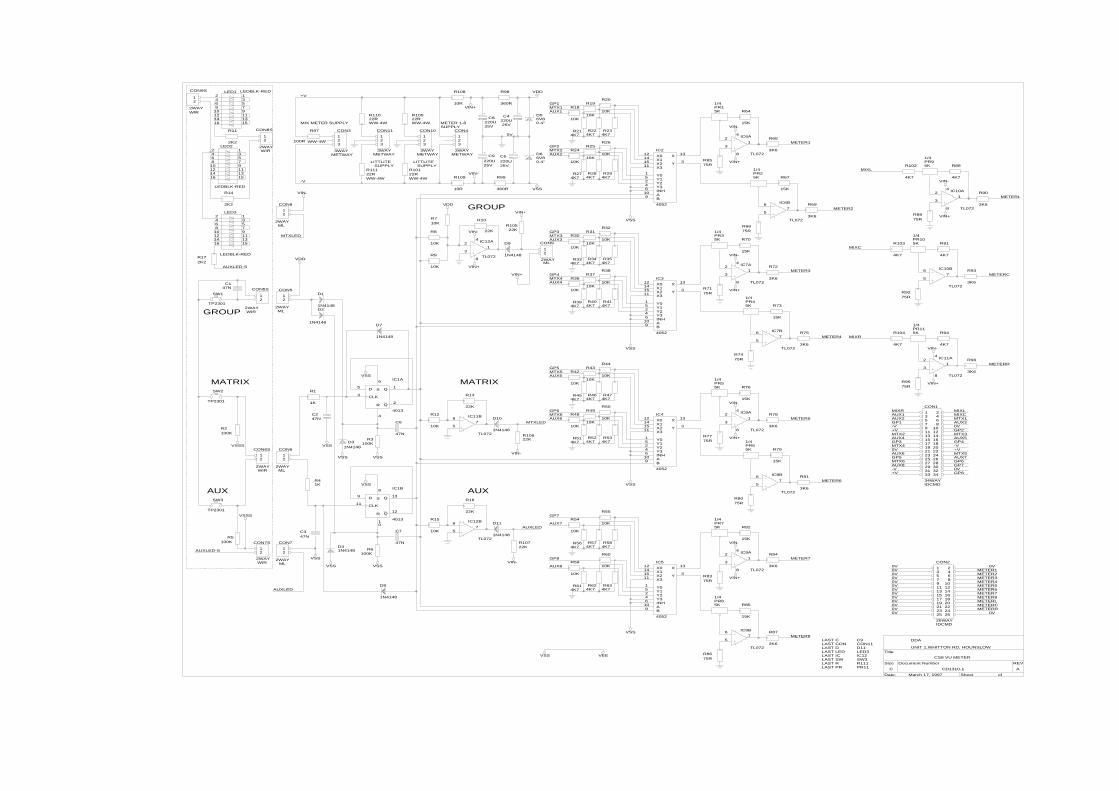
Date: March 17, 1997 Sheet of
Size Document Number REV
C CD1310-1 A
Title
CS8 VU METER
UNIT 1,WHITTON RD, HOUNSLOW
DDA
METER1 3
21
8
4 IC6A
TL072
VIN+
VIN-
R6575R
R66
3K6
R64
15K
PR15K
1/4
X0 12
X1 14
X2 15
X3 11
Y0 1
Y1 5
Y2 2
Y3 4
INH 6
A 10
B 9
X 13
Y 3
IC2
4052
R234K7
GP1MTX1AUX1
GP2MTX2AUX2
0V
VDD
R18
10K
R19
10K
R20
10K
R214K7
R224K7
R24
10K
R25
10K
R26
10K
C4220U25V
D56V80.4"
D66V80.4"
R98
360R
C5
220U25V
VIN+
METER 1-8SUPPLY
R10022RWW-4W
R108
10R
C9
220U25V
C8220U25V
123
CON10
3WAYMETWAY
123
CON4
3WAYMETWAY
MIX METER SUPPLY
R97
100R WW-4W
+V
123
CON3
3WAYMETWAY
R11022RWW-4W
123
CON11
3WAYMETWAY
12
CON8S
2WAYWIR
12
CON9S
2WAYWIR
2 4 6 8 10 12 14 16
13579111315
LED1 LEDBLK-RED
2 4 6 8 10 12 14 16
13579111315
LED2
LEDBLK-RED
R11
2K2
12
CON8
2WAYML
2 4 6 8 10 12 14 16
13579111315
LED3
LEDBLK-RED
R14
2K2
-V
VIN-
SUPPLYLITTLITE
R11122RWW-4W
GROUPVDD
R710K
R10
22K
VIN-
SUPPLYLITTLITE
R109
10R
R99
360R
R10122RWW-4W
VSS
R274K7
R284K7
R32
10K
VIN+
R10522K
R294K7
VSS
5
67
IC6B
TL072
R6875R
R69
3K6
R67
15K
PR25K
1/4 MIXL
METER2
R102
4K7
METERL 3
21
8
4 IC10A
TL072
VIN-
VIN+R8975R
R90
3K6
R88
4K7
PR95K
1/4
METERC 5
67
IC10B
TL072
R93
3K6
R91
4K7
MIXC
R9275R
PR105K
1/4
R103
4K7
METER3 3
21
8
4 IC7A
TL072
VIN+
VIN-
R7175R
R72
3K6
R70
15K
PR35K
1/4
X0 12
X1 14
X2 15
X3 11
Y0 1
Y1 5
Y2 2
Y3 4
INH 6
A 10
B 9
X 13
Y 3
IC3
4052
R354K7
R414K7
GP3MTX3AUX3
GP4MTX4AUX4
R30
10K
R31
10K
R334K7
R344K7
R36
10K
R37
10K
R38
10K
R394K7
R404K7
VIN+
12
CON9
2WAYML
D9
1N4148
VIN-
VIN+
R8
10K
R9
10K
3
21
8
4 IC12A
TL072VDD
D1
1N4148
SW1
TP2301
C147N
AUXLED-S
MTXLED
12
CON5S
2WAYWIR
12
CON5
2WAYML
R172K2
GROUP
VSS
D7
1N4148
D2
1N4148
GP5MTX5AUX5
R42
10K
R43
10K
R44
10K
VSS
5
67
IC7B
TL072
R7475R
R75
3K6
R73
15K
PR45K
1/4
MIXRMETER4
R9575R
PR115K
1/4
R104
4K7
METERR 3
21
8
4 IC11A
TL072
VIN-
VIN+
R96
3K6
R94
4K7
MIXCMIXL
MTX1
GP2
AUX3
GP4AUX5
-V+V
0V
MTX3
1 23 45 67 89 1011 1213 1415 1617 1819 2021 2223 2425 2627 2829 3031 3233 34
CON1
34WAYIDCMD
MIXR
GP1
AUX1
MTX2
AUX2
GP3MTX4
AUX4
-V+V
0V
METER5 3
21
8
4 IC8A
TL072
VIN+
VIN-
R7775R
R78
3K6
R76
15K
R79
15K
PR55K
1/4
PR65K
1/4
X0 12
X1 14
X2 15
X3 11
Y0 1
Y1 5
Y2 2
Y3 4
INH 6
A 10
B 9
X 13
Y 3
IC4
4052
R474K7
R534K7
GP6MTX6AUX6
R49
10K
R454K7
R464K7
R48
10K
R50
10K
R514K7
R524K7
MTXLED
VIN-
R10622K
MATRIX
R12
10K
R13
22K
C6
47N
5
67
IC11B
TL072
D10
1N4148
VSSVSS
VSS
R1
1K
R3100K
C247N
D3
1N4148
D 5 Q 1
CLK 3
Q 2R
4
S
6 IC1A
4013
MATRIX
R2100K
SW2
TP2301
12
CON6S
2WAYWIR
12
CON6
2WAYML
VSSS
AUXSW3
TP2301
VSSS
D 9 Q 13
CLK 11
Q 12R
10
S
8 IC1B
4013
VSSR41K
AUX
R15
10K
R16
22K
5
67
IC12B
TL072
D11
1N4148
GP7
AUX7R54
10K
R55
10K
VSS 5
67
IC8B
TL072
R8075R
R81
3K6
METER6
GP5MTX6
AUX6
AUX8-V+V
MTX5
GP6GP7
AUX7
GP80V
0VMETER1METER2METER3METER4METER5METER6METER7METER8
1 23 45 67 89 1011 1213 1415 1617 1819 2021 2223 2425 26
CON2
26WAYIDCMD
0V
0V0V0V0V0V0V0V0V
METER7 3
21
8
4IC9A
TL072
VIN+
VIN-
R8375R
R84
3K6
R82
15K
PR75K
1/4
X0 12
X1 14
X2 15
X3 11
Y0 1
Y1 5
Y2 2
Y3 4
INH 6
A 10
B 9
X 13
Y 3
IC5
4052
R584K7
R634K7
GP8
AUX8
R564K7
R574K7
R59
10K
R60
10K
R614K7
R624K7
AUXLED
VIN-
R10722K
C7
47N
VSS
VSS VSS
R6100K
C347N
D41N4148
D8
1N4148
R5100K
AUXLED-S
AUXLED
12
CON7S
2WAYWIR
12
CON7
2WAYML
VSS
VSS
VEE
METER8 5
67
IC9B
TL072
R8675R
R87
3K6
R85
15K
PR85K
1/4
LAST CLAST CONLAST DLAST LEDLAST ICLAST SW
LAST PR
LED3
0V0V0V0V
LAST R
C9
IC12SW3
PR11
CON11
R111
D11
0V
METERLMETERCMETERR

Date: February 13, 1997 Sheet 1 of 1
Size Document Number REV
B CD1309-1 A
Title
CS8 METERS CONNECTOR
DDA, HOUNSLOW, MIDDX, TW3 2EB, ENGLAND.
SIG1SIG3
1 23 45 67 89 1011 1213 1415 1617 1819 2021 2223 2425 26
CON1
26WAYIDCMD
SIG1SIG3
SIG2SIG4
SIG2SIG4
1 23 45 67 89 1011 1213 1415 1617 1819 2021 2223 2425 2627 2829 3031 3233 34
CON2
34WYIDCBXR
MIXRAUX1
1 23 45 67 89 1011 1213 1415 1617 1819 2021 2223 2425 26
CON5
26WAYIDCMD
MIXCMIXL MIXR
AUX11 23 45 67 89 1011 1213 1415 1617 1819 2021 2223 2425 2627 2829 3031 3233 34
CON6
34WYIDCBXR
MIXCMIXL
MTX1
GP2
AUX3
GP4
MTX5
AUX5
GP6GP7
AUX7
-V+V
0V
MTX3
GP1
MTX2
AUX2
GP3MTX4
AUX4
GP5MTX6
AUX6
AUX8
-V+V
0V
MTX1
GP2MTX3
AUX3
GP4MTX5
AUX5
GP6GP7
AUX7
GP1MTX2
AUX2
GP3MTX4
AUX4
GP5MTX6
AUX6
GP8AUX8
SIG6SIG80VSIG9SIG11SIG13SIG15-V+VSIG18SIG20SIG22SIG24
SIG5SIG7
SIG10SIG12SIG14SIG16
SIG17
SIG6SIG8SIG10SIG12SIG14SIG16SIG18SIG20SIG22SIG24
-V+V
0V
SIG19SIG21SIG23
SIG5SIG7SIG9SIG11SIG13SIG15SIG17SIG19SIG21SIG23
INPUT 1-24
-V+V
0V
OUTPUT & MASTERS
-V+V GP8
0V
0V
SIG26SIG28SIG30SIG32
SIG33
1 23 45 67 89 1011 1213 1415 1617 1819 2021 2223 2425 2627 2829 3031 3233 34
CON4
34WYIDCBXR
SIG34SIG36
-V+V
SIG26SIG28SIG30SIG32
SIG25SIG27SIG29SIG31
1 23 45 67 89 1011 1213 1415 1617 1819 2021 2223 2425 26
CON3
26WAYIDCMD
SIG35
SIG25SIG27SIG29SIG31SIG33
SIG37SIG39SIG41SIG43SIG45SIG47
SIG34SIG36SIG38SIG40
SIG41
SIG38SIG40SIG42SIG44SIG46SIG48
0V
SIG43SIG45SIG47-V+V
SIG35SIG37SIG39-V+VSIG42SIG44SIG46SIG480V
+V123
CON7
3WAYMH156
-V0V
INPUT 25-48