development of application specific integrated circuits ... review... · asics for cadmium zinc...
TRANSCRIPT
Instrumentation Division
Microelectronics
managed by Brookhaven Science Associatesfor the U.S. Department of Energy
Gianluigi De Geronimo, Ph.D.
Presentation to the DOE NP Program ReviewJULY 19, 2007
Development of Application Specific Integrated Circuits (ASICs) for DOE/BNL
Experimental Research Programs
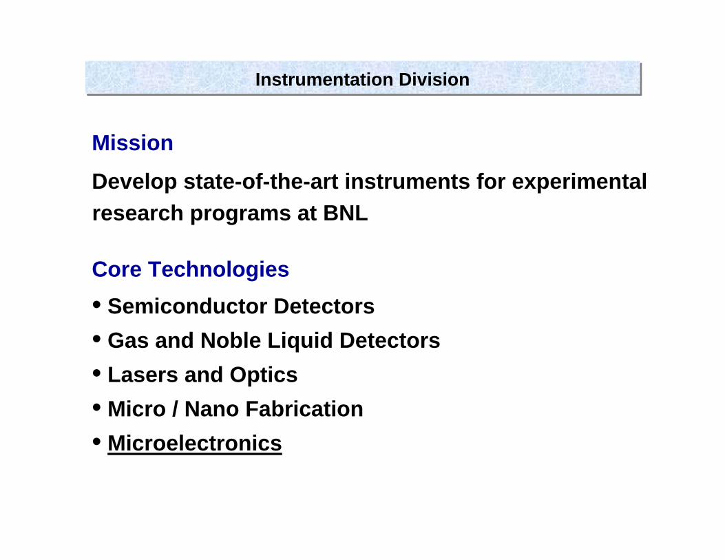
Mission
Develop state-of-the-art instruments for experimental research programs at BNL
Core Technologies• Semiconductor Detectors• Gas and Noble Liquid Detectors• Lasers and Optics• Micro / Nano Fabrication• Microelectronics
Instrumentation DivisionInstrumentation Division
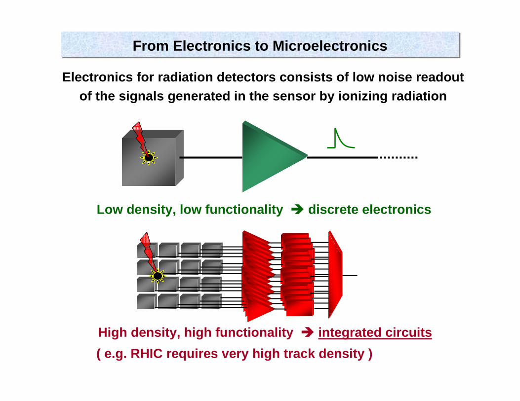
From Electronics to MicroelectronicsFrom Electronics to Microelectronics
Low density, low functionality discrete electronics
Electronics for radiation detectors consists of low noise readoutof the signals generated in the sensor by ionizing radiation
High density, high functionality integrated circuits( e.g. RHIC requires very high track density )

IntegrationIntegration
sensing element
filtering(shaping),stabilization
discrimination, amplitude / timing extraction
sparsification, derandomization, multiplexing
A/D conversion, data processing
low-noisecharge amplifier
Typical electronics channel
year 2000· 0.5 µm technology· 16,000 transistors· 16 channels· analog
ASICfunctions
ASICfunctions
year 2006· 0.18 µm technology· 600,000 transistors· 128 channels· analog and digital(mixed-signal)

ASIC Design FlowASIC Design Flow
Higher complexity means more resources and expertise, longer development time
and ultimately higher risk
revision cycle
designphase
system level
design
transistorlevel
design maskslayout fabrication tests
months 2 6 2 3 2
From concept to ready-for-production:2 - 3 years (depending on complexity)
First report after~ 15 months
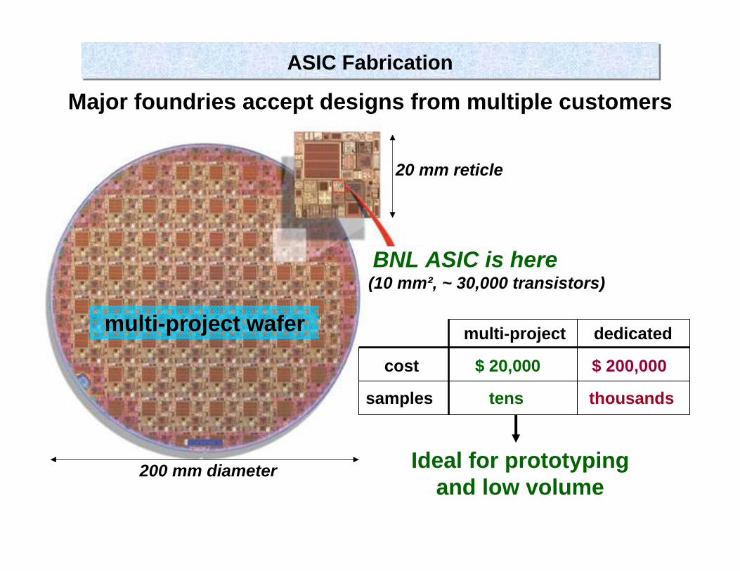
ASIC FabricationASIC Fabrication
Major foundries accept designs from multiple customers
multi-project wafer
20 mm reticle
200 mm diameter Ideal for prototyping and low volume
BNL ASIC is here(10 mm², ~ 30,000 transistors)
multi-project dedicated
cost $ 20,000 $ 200,000
samples tens thousands

In the last 10 years we developed more than 30 ASICs for applications in:
Particle and Nuclear Physics
X- and Gamma-Ray Spectroscopy and Imaging
Medical, Security, Industrial
We have an established worldwide reputation as leaders in low-noise ASIC design
About our groupAbout our group

Some recent examples …

Front-End ASIC for the STAR SVT at RHICFront-End ASIC for the STAR SVT at RHIC
3.3 x 2.4 mm²
16 channels, 3.8 mW/channelCharge amplifier and shaper NPN-BJT process380 e- resolution at 50 ns
16 channels, 3.8 mW/channelCharge amplifier and shaper NPN-BJT process380 e- resolution at 50 ns
A 240 Channel Multi-Chip Module for Readout of Silicon Drift Detectors
D. DiMassimo et al.
D. Lynn et al.
30,720 pixels (128 modules)240 channel multi-chip modulePASA and SCA ASICs10-bit DR, 3 ns timing resolution
30,720 pixels (128 modules)240 channel multi-chip modulePASA and SCA ASICs10-bit DR, 3 ns timing resolution

ASIC for the Laser Electron Gamma Source TPCASIC for the Laser Electron Gamma Source TPC
3.1 x 3.6 mm²
G. De Geronimo et al., TNS (2004)
Gas Electron Multiplier
8000 anode pads read out inless than 400 µs due to unique sparse readout
32 channels230 e-, 2.5 ns resol.sparse readoutneighboring40,000 transistorsdev. time: 16 months
32 channels230 e-, 2.5 ns resol.sparse readoutneighboring40,000 transistorsdev. time: 16 months
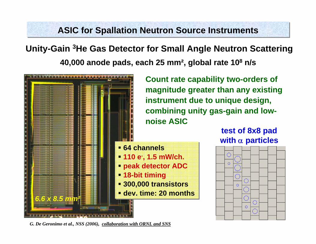
ASIC for Spallation Neutron Source InstrumentsASIC for Spallation Neutron Source Instruments
64 channels110 e-, 1.5 mW/ch.peak detector ADC18-bit timing300,000 transistorsdev. time: 20 months
64 channels110 e-, 1.5 mW/ch.peak detector ADC18-bit timing300,000 transistorsdev. time: 20 months
6.6 x 8.5 mm²
Unity-Gain 3He Gas Detector for Small Angle Neutron Scattering40,000 anode pads, each 25 mm², global rate 108 n/s
Count rate capability two-orders of magnitude greater than any existing instrument due to unique design, combining unity gas-gain and low-noise ASIC
G. De Geronimo et al., NSS (2006), collaboration with ORNL and SNS
test of 8x8 padwith α particles
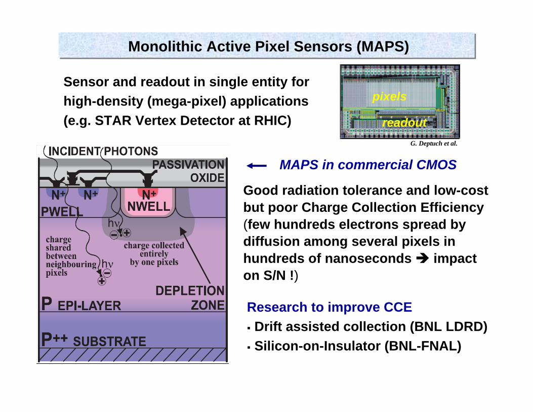
Monolithic Active Pixel Sensors (MAPS)Monolithic Active Pixel Sensors (MAPS)
Sensor and readout in single entity forhigh-density (mega-pixel) applications (e.g. STAR Vertex Detector at RHIC)
MAPS in commercial CMOS
Good radiation tolerance and low-cost but poor Charge Collection Efficiency (few hundreds electrons spread by diffusion among several pixels in hundreds of nanoseconds impact on S/N !)
pixels
readoutG. Deptuch et al.
Research to improve CCEDrift assisted collection (BNL LDRD)Silicon-on-Insulator (BNL-FNAL)

ASICs for Synchrotron ApplicationsASICs for Synchrotron Applications
G. De Geronimo et al.
For high-rate high-resolution spectroscopy and photon-counting experiments at NSLS and NSLS-II
(EXAFS, powder diffraction, fluorescence microprobes)
32 channels front-endsub-20 electrons resolutionspectroscopy, photon-countinghigh-rate 180,000 transistors
32 channels front-endsub-20 electrons resolutionspectroscopy, photon-countinghigh-rate 180,000 transistors
32 channels processingpeak detection, sparsification,
derandomization, multiplexingenergy, timing and address high rate36,000 transistors
32 channels processingpeak detection, sparsification,
derandomization, multiplexingenergy, timing and address high rate36,000 transistors
HERMES SCEPTER
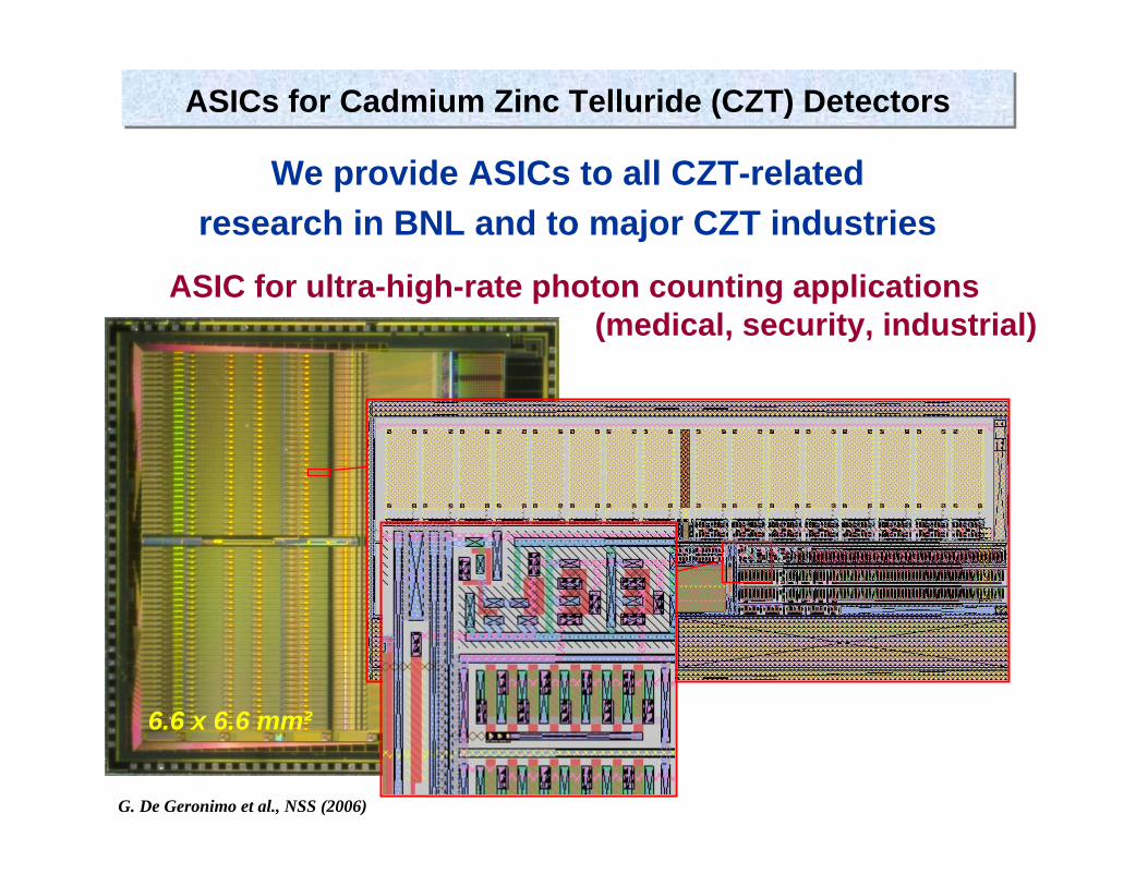
ASICs for Cadmium Zinc Telluride (CZT) DetectorsASICs for Cadmium Zinc Telluride (CZT) Detectors
We provide ASICs to all CZT-relatedresearch in BNL and to major CZT industries
G. De Geronimo et al., NSS (2006)
6.6 x 6.6 mm²
64 channelsvery fast shaper (40ns, 9th order)five energy windows per channelmega-counts s-1 per channel600,000 transistorsdev. time: 20 months
64 channelsvery fast shaper (40ns, 9th order)five energy windows per channelmega-counts s-1 per channel600,000 transistorsdev. time: 20 months
ASIC for ultra-high-rate photon counting applications(medical, security, industrial)
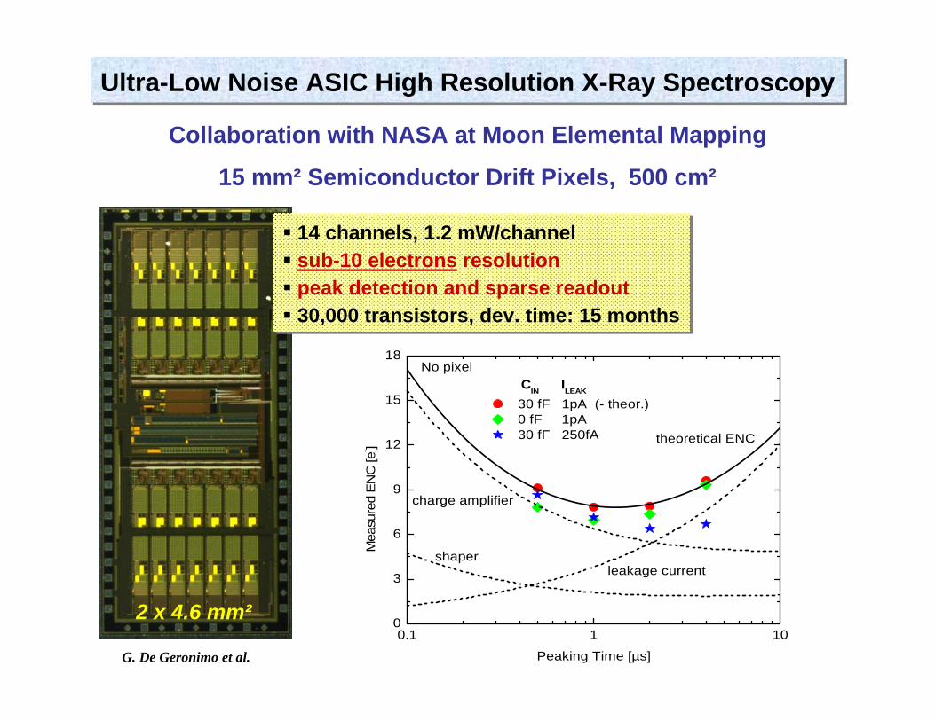
Ultra-Low Noise ASIC High Resolution X-Ray SpectroscopyUltra-Low Noise ASIC High Resolution X-Ray Spectroscopy
2 x 4.6 mm²
14 channels, 1.2 mW/channelsub-10 electrons resolutionpeak detection and sparse readout30,000 transistors, dev. time: 15 months
14 channels, 1.2 mW/channelsub-10 electrons resolutionpeak detection and sparse readout30,000 transistors, dev. time: 15 months
Collaboration with NASA at Moon Elemental Mapping
G. De Geronimo et al.
15 mm² Semiconductor Drift Pixels, 500 cm²
0.1 1 100
3
6
9
12
15
18No pixel
theoretical ENC
leakage current
charge amplifier
CIN ILEAK
30 fF 1pA (- theor.) 0 fF 1pA 30 fF 250fA
Mea
sure
d EN
C [e
- ]
Peaking Time [µs]
shaper
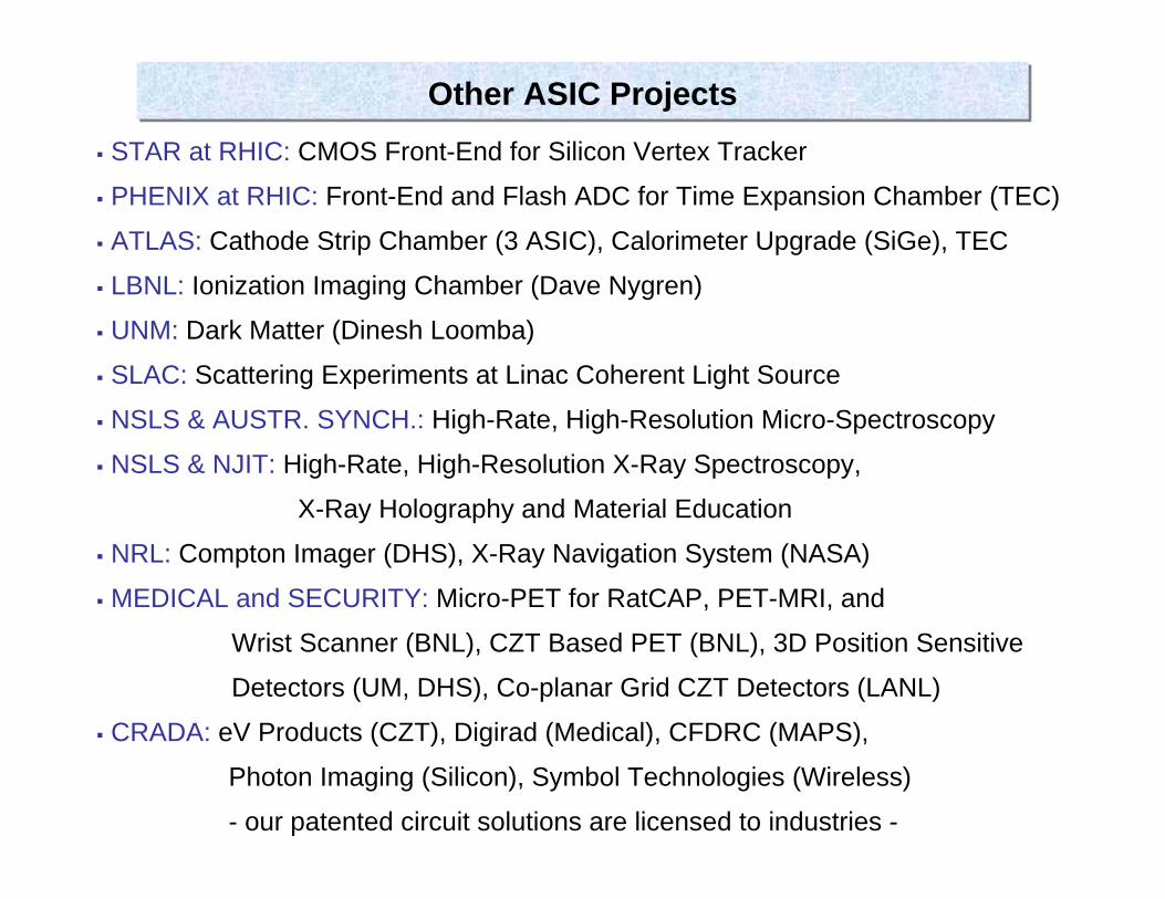
Other ASIC ProjectsOther ASIC ProjectsSTAR at RHIC: CMOS Front-End for Silicon Vertex Tracker
PHENIX at RHIC: Front-End and Flash ADC for Time Expansion Chamber (TEC)
ATLAS: Cathode Strip Chamber (3 ASIC), Calorimeter Upgrade (SiGe), TEC
LBNL: Ionization Imaging Chamber (Dave Nygren)
UNM: Dark Matter (Dinesh Loomba)
SLAC: Scattering Experiments at Linac Coherent Light Source
NSLS & AUSTR. SYNCH.: High-Rate, High-Resolution Micro-Spectroscopy
NSLS & NJIT: High-Rate, High-Resolution X-Ray Spectroscopy,
X-Ray Holography and Material Education
NRL: Compton Imager (DHS), X-Ray Navigation System (NASA)
MEDICAL and SECURITY: Micro-PET for RatCAP, PET-MRI, and
Wrist Scanner (BNL), CZT Based PET (BNL), 3D Position Sensitive
Detectors (UM, DHS), Co-planar Grid CZT Detectors (LANL)
CRADA: eV Products (CZT), Digirad (Medical), CFDRC (MAPS),
Photon Imaging (Silicon), Symbol Technologies (Wireless)
- our patented circuit solutions are licensed to industries -