digital 2 : ekt 221 date : 15 th july 2005 lecture : 1 hrs
TRANSCRIPT

DIGITAL 2 : EKT 221
Date : 15th July 2005
Lecture : 1 hrs

Reminder
Mini Project – group of 4 persons from the same program
Dateline for group formation – Next week Friday (22/7/2005)
Dateline for project title, synopsis @ paperwork submission (20/8/2005)
Project samples – to give as handoutsProject requirements – to give as
handouts

Mini Project Marking Scheme
Presentation (50 marks) Project explaination (comprehensiveness) - 20 Attitude & Attire -10 Team Coordination - 10 Add-ons (Project Details) - 10
Posters, Flowcharts

Mini Project Marking Scheme
Creativity (30 marks) Digital Design Development – 15
Complexity of Design Originality
Hardware Skills - 15 Additional Circuit Development Order of Development
(Systematic, tidiness and orderly)

Mini Project Marking Scheme
Jury Evaluation (10 marks) Communication level among group members Contribution level among group members
Peer Evaluation (10 marks) Based on group members’ evaluation
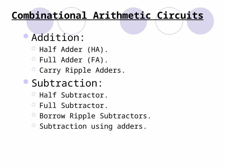
Combinational Arithmetic Circuits
Addition: Half Adder (HA). Full Adder (FA). Carry Ripple Adders.
Subtraction: Half Subtractor. Full Subtractor. Borrow Ripple Subtractors. Subtraction using adders.

Half Adder
X0011
Y0101
S0110
C-out 0 0 0 1
Half Adder Truth Table:
Inputs Outputs
S = X Y
C-out = XY
X
YSum S
C-out HalfAdder
X
Y
SC-OUT

Full Adder
X00001111
Y00110011
S01101001
C-out 0 0 0 1 0 1 1 1
C-in 0 1 0 1 0 1 0 1
Full Adder Truth Table
S(X,Y, C-in) = (1,2,4,7)C-out(x, y, C-in) = (3,5,6,7)
Inputs Outputs S = X Y (C-in)
C-out = XY + X(C-in) + Y(C-in)
Full Adder
X Y
S
C-inC-out

Full Adder
X1 Y1
S1
C-inC-out Full Adder
X0 Y0
S0
C-inC-out C0 =0 Full Adder
X2 Y2
S2
C-inC-out Full Adder
X3 Y3
S3
C-inC-outC1C2C3C4
Data inputs to be added
Sum output
4-bit Carry Ripple Adder
4-bit Adder
X3X2X1X0
S3 S2 S1 S0
C-inC-outC4
Y3Y2Y1Y0
C0 =0
Inputs to be added
Sum Output
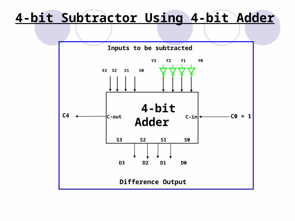
4-bit Subtractor Using 4-bit Adder
4-bit Adder
X3 X2 X1 X0
D3 D2 D1 D0
C-inC-outC4
Y3 Y2 Y1 Y0
C0 = 1
Inputs to be subtracted
Difference Output
S3 S2 S1 S0
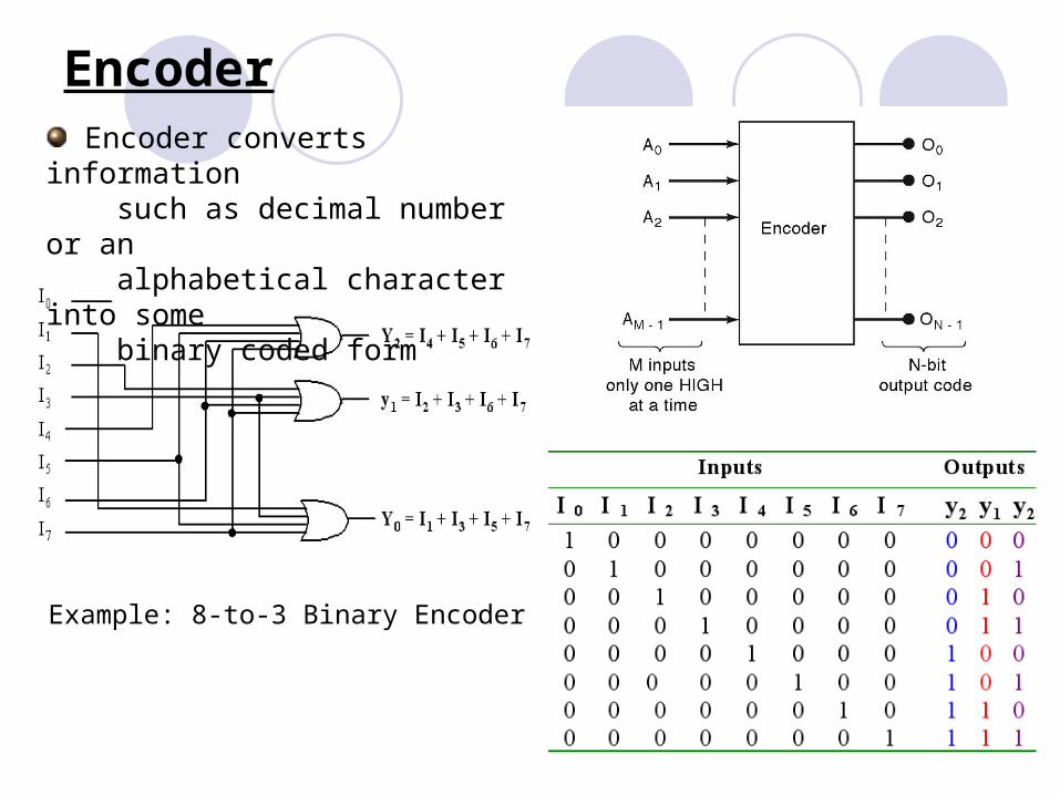
Encoder Encoder converts information
such as decimal number or an alphabetical character into some binary coded form
Example: 8-to-3 Binary Encoder

DecoderExample: 3 to 8 Binary Decoder
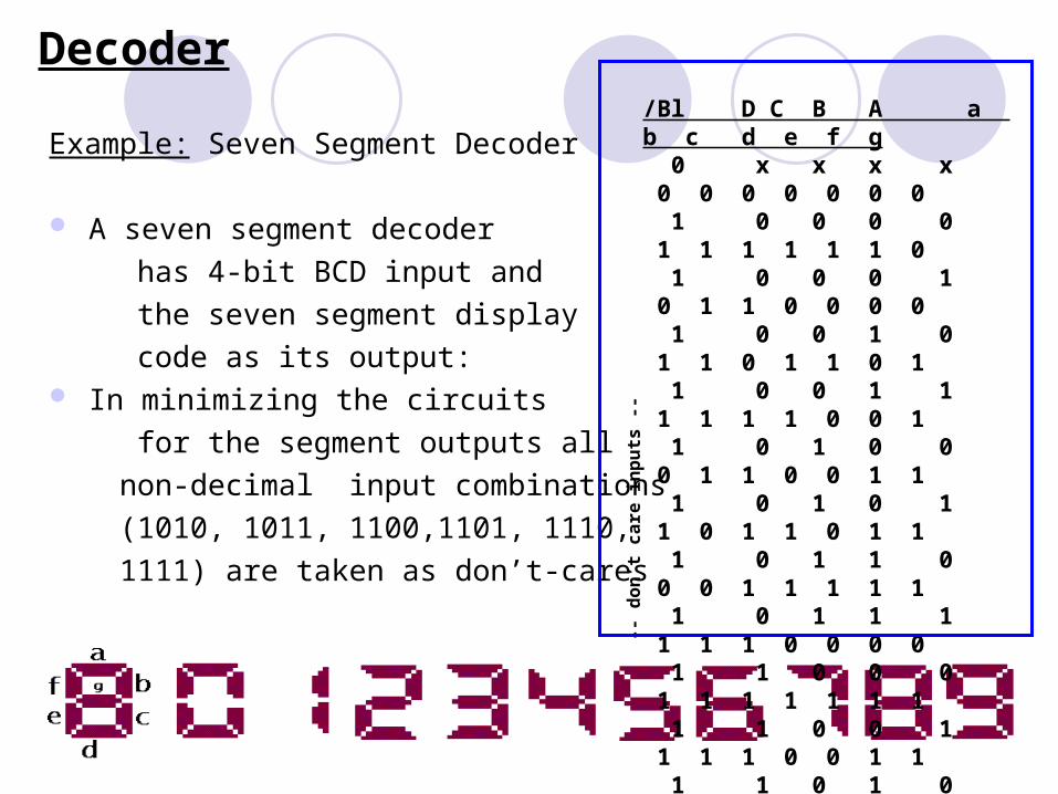
Decoder
Example: Seven Segment Decoder
A seven segment decoder
has 4-bit BCD input and
the seven segment display
code as its output: In minimizing the circuits
for the segment outputs all
non-decimal input combinations
(1010, 1011, 1100,1101, 1110,
1111) are taken as don’t-cares
/Bl D C B A a b c d e f g 0 x x x x 0 0 0 0 0 0 0 1 0 0 0 0 1 1 1 1 1 1 0 1 0 0 0 1 0 1 1 0 0 0 0 1 0 0 1 0 1 1 0 1 1 0 1 1 0 0 1 1 1 1 1 1 0 0 1 1 0 1 0 0 0 1 1 0 0 1 1 1 0 1 0 1 1 0 1 1 0 1 1 1 0 1 1 0 0 0 1 1 1 1 1 1 0 1 1 1 1 1 1 0 0 0 0 1 1 0 0 0 1 1 1 1 1 1 1 1 1 0 0 1 1 1 1 0 0 1 1 1 1 0 1 0 0 0 0 1 1 0 1 1 1 0 1 1 0 0 1 1 0 0 1 1 1 1 0 0 0 1 0 0 0 1 1 1 1 1 0 1 1 0 0 1 0 1 1 1 1 1 1 0 0 0 0 1 1 1 1 1 1 1 1 1 0 0 0 0 0 0 0
-- d
on’t
car
e in
pu
ts -
-

Multiplexer
A 4 input multiplexer

DemultiplexerExample: 1- to -4 Demultiplexer

Latches: S-R Latch Gate S-R Latch Gate D-Latch
Flip-Flops: Edge-Triggered Flip-Flop (S-R, J-K, D) Asynchronous Inputs Master-Slave Flip-Flop Flip-Flop Operating Characteristics Flip-Flop Applications One-shots & The 555 Timer
Latches & Flip Flop

Latches & Flip Flop
Truth Table for each FF+ve / -ve edge triggeredWaveform

JKFF Transition Table
J K Qt if Qt Qt + 1
0 0 n.c0
1
0 1 00
1
1 0 10
1
1 1 T0
1
Derive the from this equation to get JKFF Transition Table

JKFF Transition Table
Qt Qt+1 J K
0 0 0 x
0 1 1 x
1 0 x 1
1 1 x 0
Note : This Transition Table will be useful in your LAB 4 : Sequential Up/Down Binary Counter

Basic shift register functionSerial in / serial out shift registersSerial in / parallel out shift registersParallel in / serial out shift registersParallel in / parallel out shift registersBidirectional shift registersShift register applications
Shift Register

Serial In, Serial Out Shift Register(SISO)

Serial In, Parallel Out Shift register (SIPO)
• Data bits entered serially (right-most bit first)
• Difference from SISO is the way data bits are taken
out of the register – in parallel.
• Output of each stage is available

Parallel In, Parallel Out Shift Register (PIPO)
Immediately following simultaneous entry of all data bits,it appear on parallel output.

ASYNCHRONOUS COUNTER:
A 2-bit asynchronous binary counter.
•Don’t have fixed time relationship with each other.
•Don’t occur at the same time.
•Don’t have a common clock pulse

SYNCHRONOUS COUNTER OPERATION A 2-bit synchronous binary counter.

UP/DOWN SYNCHRONOUS COUNTER
A basic 3-bit up/down synchronous counter.

Reminder
Your “Digital Fundamental” book is still essential for basic reference to this course.
Do NOT sell it yet !!

THANK YOU