digital circuits prof. santanu chattopadhyay department of … · 2018-11-02 · and gate, or gate,...
TRANSCRIPT
Digital CircuitsProf. Santanu Chattopadhyay
Department of Electronics and Electrical Communication EngineeringIndian Institute of Technology, Kharagpur
Lecture - 17Logic Gates (Contd.)
So, we will be looking to static CMOS logic family. Why static so, we will come to that
later, but as I have said that CMOS is the de facto standard for this digital circuit, digital
gate realization. Now, we will we will see that in successive slides.
(Refer Slide Time: 00:35)
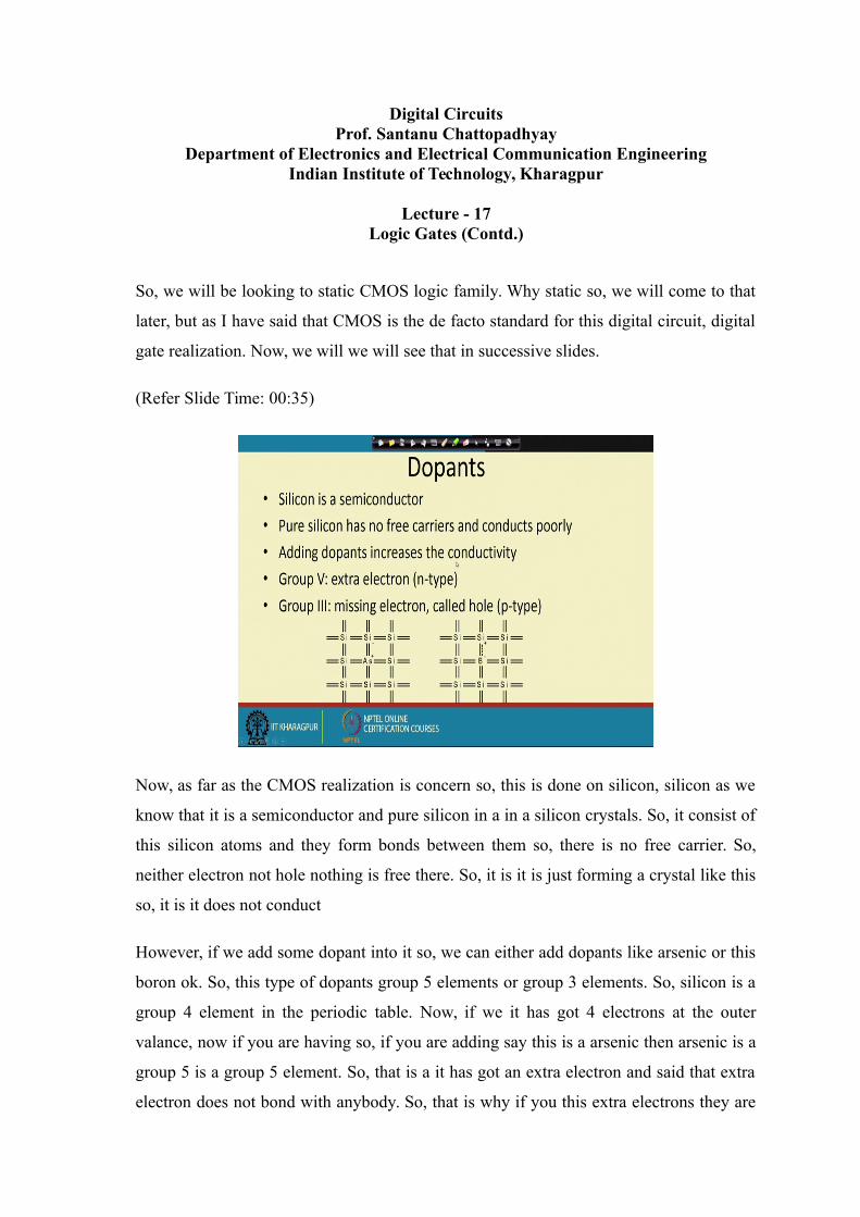
Now, as far as the CMOS realization is concern so, this is done on silicon, silicon as we
know that it is a semiconductor and pure silicon in a in a silicon crystals. So, it consist of
this silicon atoms and they form bonds between them so, there is no free carrier. So,
neither electron not hole nothing is free there. So, it is it is just forming a crystal like this
so, it is it does not conduct
However, if we add some dopant into it so, we can either add dopants like arsenic or this
boron ok. So, this type of dopants group 5 elements or group 3 elements. So, silicon is a
group 4 element in the periodic table. Now, if we it has got 4 electrons at the outer
valance, now if you are having so, if you are adding say this is a arsenic then arsenic is a
group 5 is a group 5 element. So, that is a it has got an extra electron and said that extra
electron does not bond with anybody. So, that is why if you this extra electrons they are

they can move freely ok. So, if you apply some potential then this electrons can be made
to flow very easily.
So, by adding this extra electron in the so, or doping the pure silicon with arsenic so, we
get something called n-types semiconductor. In an n-type semiconductor we have got
plenty of electrons available which can be made to flow if we apply some potential
difference. On the other hand, so instead of applying a group 5 dopants; so if we apply a
group 3 dopant so, group 3 dopant we have got 3 electrons at the outer valiancy. So,
there it has got a tendency to capture one more electron. So, in some sense it is like a
hole that is there in the outer valance.
So, that is why this type of dopants so, they are called donor and they are called acceptor
and these this has got a hole ok. So, group 3 they have go missing electron as if as if it
has got a hole and this type of semiconductors that you get so, they are called they are
they are p-type dopant.
And if you put this boron type of impurity into this silicon crystal silicon vapor then we
will get a p-type semiconductor ok. So, this is both n-type and p-type semiconductors are
there in realizing different circuits like starting your diode to transistors to MOS and all.
So, we will using them particularly in the context of this MOS transistors.
(Refer Slide Time: 03:10)

So, a basic nMOS transistor the operation is like this so, we have got this bulk silicon.
So, this is the bulk silicon so, this bulk silicon so, we can say it is an vapor of silicon and
this is a p-type silicon. So, this is a doped with boron so, that this is a p this is the this
rectangular region that we have drawn so, you can take it as a p-type semiconductor.
Now, on that we have got two heavily doped region of p-type semi of n-type
semiconductors ok. So, there that is done by means of this diffusion process that you can
learn in some course on VLSI design. So, this is the some diffusion is done so, that you
get this n-plus regions twos two such n-plus regions. Between the two n-plus region so,
we have got a silicon dioxide layer which is an insulating material and on top of the
silicon dioxide layer so, we have got a diffusion of this poly silicon layer. So, we have
got a deposition of poly silicon
So, what happens is that if you if you do not apply any extra potential ok. So, this p-type
voltage p type so, this is the body or the bulk silicon so, this is kept at a low voltage.
Now, if this source body and drain body diodes are OFF. So, how can this be OFF? So, if
you do not apply any voltage to this source and drain all these diodes are off so, so there
will be no current flow.
However, if you apply some positive voltage in the gate; so if I apply some positive
voltage in the gate then what will happen; electrons that are there in this substrate this p-
type substrate. So, they will be drawn toward this region, they will be drawn towards this
region. So, we have got the electrons coming here.
So, so for I have applied only some gate voltage I have not applied any voltage at source
and drain. Now, if you apply some a voltage difference between source and drain ok,
then this electrons may be made to flow from one side to the other; like if we make this
drain voltage high and this source voltage low then the electrons will be drawn towards
the drain as a result as a current will flow from drain to source.
So, when I do not apply any gate voltage. So, this transistor is OFF, but as we are
applying some voltage gate voltage the transistor is this on and if we have a potential
difference between drain and source then the current will flow through the device. So,
pictorially, it is represented by a symb situation by a symbol like this. So, this is so, this
particular symbol we have got two terminal source and drain and then the other terminal.
So, this is called the gate or G ok. So, this is called the gate or G. So, when G equal to 0
then this source drain there is no current flow between source and drain, otherwise there
will be a current flow.
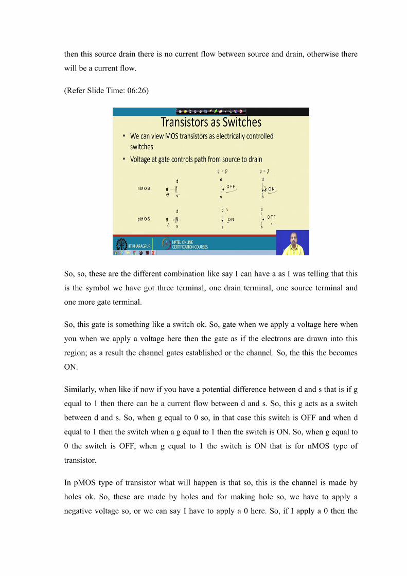
(Refer Slide Time: 06:26)
So, so, these are the different combination like say I can have a as I was telling that this
is the symbol we have got three terminal, one drain terminal, one source terminal and
one more gate terminal.
So, this gate is something like a switch ok. So, gate when we apply a voltage here when
you when we apply a voltage here then the gate as if the electrons are drawn into this
region; as a result the channel gates established or the channel. So, the this the becomes
ON.
Similarly, when like if now if you have a potential difference between d and s that is if g
equal to 1 then there can be a current flow between d and s. So, this g acts as a switch
between d and s. So, when g equal to 0 so, in that case this switch is OFF and when d
equal to 1 then the switch when a g equal to 1 then the switch is ON. So, when g equal to
0 the switch is OFF, when g equal to 1 the switch is ON that is for nMOS type of
transistor.
In pMOS type of transistor what will happen is that so, this is the channel is made by
holes ok. So, these are made by holes and for making hole so, we have to apply a
negative voltage so, or we can say I have to apply a 0 here. So, if I apply a 0 then the

pMOS transistor is ON and if I apply a 1 then the pMOS transistor is OFF. So, this way
this by controlling this gate voltage so, we can consider the transistor to be ON or
transistor to be OFF. For nMOS transistor it is ON if g equal to 0 and it is OFF sorry it is
OFF if g equal to 0 and it is ON if g equal to 1. For pMOS transistor it is ON if gate
equal to 0 g equal to 0 and it is OFF if g equal to 1.
So, in so, we can use either of this two types of transistors nMOS and pMOS transistors
and different logic families have been built, like say nMOS family that I have said. So,
that actually uses this nMOS type of transistors to get a different types of gates like a
AND gate, OR gate, NAND gate like that; pMOS also can be used for that.
And in a CMOS so, we have got both nMOS and pMOS transistors for realizing the logic
circuit logic gates ok.
(Refer Slide Time: 08:57)
So, a CMOS inverter looks like this so, we have got this is the symbol of a CMOS
invertor. So, upper transistor so, whenever we have got a bubble here so, this means this
is a p-type transistor. So, this is a p-type transistor and this is an n-type transistor. So, p-
type transistor means if g if I say this is g so, this is say g 1 and so, this is say g 2 when g
1 is equal to 0 then p is ON, when g 1 equal to 1 p is OFF ok. Similarly, for n-type
transistor if g 2 equal to 0 then the n-type transistor is OFF then n is OFF and if g is
equal to g if g 2 equal to 1 then n is ON. So, this is the situation

Now, let us consider the case where this 2 gate terminals of this p-type transistor and n-
type transistor they have shorted and the input A is applied to both of them. Now, what
happens? Now, if A equal to 0 so, if A equal to 0 in that case this transistor is as per this
writing. So, as per as this transistor is ON and this transistor is OFF fine; so this transi
upper transistor is ON and lower transistor is OFF.
Now, if I measure the voltage here how much what is the value I will get. So, I will get a
value close to V D D that a V D D is say high so, this is this is say some 5 volt then I will
get a 5 volt here. So, I can say if A is equal to 0 then I am getting Y as 1 logic high which
is say equal to 5 volt. Now, if A equal to 1 in that case what I will get I so, in that case
this p is OFF. So, this is OFF now and this is ON now, the lower transistor is ON now.
Now, if I measure the voltage here I will get a value close to this ground potential which
is 0. So, I can say if it is 1 then I will get a 0 there.
So, what is this functionality this is nothing, but an inverter. So, it is so, I can say this is
an inverter when A equal to 1 Y is equal to 0 when A equal to 0 y equal to 1. So, this
basic circuit so, this basic circuit acts as an inverter and it has got 2 transistors of two
different type nMOS transistor and pMOS transistor. So, we call it; that is why it is called
as CMOS inverter so, it has got complementary metal oxide semiconductor inverter.
So, complementary means it has got both p and n components in it and the input is
feeding to both the n transistor as well as the p transistor. So, this way I can have this
CMOS transistor CMOS inverter.

(Refer Slide Time: 12:13)
So, next we will be looking into a cross section like how this CMOS transis CMOS
inverter looks like if I just take such a device which is nMOS inverter and take a cross
section of it. So, normally what is what is done is that so, for as we have said you seen in
the first slide. So, we have got a p type substrate on to which we have got this we have
got the n n type regions.
So, we have got p type substrate on to which we have got this n plus regions for the drain
and source and then we in between we have got silicon, this is a silicon dioxide and here
we have got the gate ok. So, this is the poly silicon gate that we have so, these are the
ligands that we have used.
Now, you see that these inputs are so, if this is the source, this is the drain so, this is the
source and this is. So, for the for the p type transistor what we have to do is I cannot use
a p type substrate I have to use an n type substrate. So, for that what is done within this p
type substrate one n type well is found ok, region where I do some n diffusion. So, it
creates an n type well and within this n type well so, we do this p plus type of diffusion
to create the p plus regions.
Now, using this metal using this metal line so, this is a blue colored regions. So, this
region you see that these two are shorted so; that means, the there is drain of the p n
transistor and the source of p transistor so, they are shorted. So, if I draw in terms of

diagram like if the lower transistor is the n type transi lower transistor is the n type
transistor so, this the source. So, this end this point is that S that I have.
So, this gate is there then this drain is connected to the source of the p transistor. So, this
is nothing, but something like this so, this is the p transistor ok. So, this the drain and this
is the source of this is the drain of p and this is the so, sorry. So, this is the source of p
and this is the drain of n. So, they are shorted. Similarly, the drain of p so, it is connected
to V D D.
So, this is connected to V D D as it is shown here and we have got these 2 terminals
these 2 gates are available so, these two are to be shorted ok. So, these two are to be
shorted and the A input has to be connected here and I have to take output from this point
ok. So, this is the shorting out of from the two shorting so, this is the Y output which is
going out. So, we can I have I can put some additional metal lines to connect short the 2
gate inputs and apply A here. So, as it is shown here that the A is applied to both of them
and Y is taken from here.
So, this way we can have a n type sorry we can have the CMOS inverter implemented
using this CMOS technology. So, this A is going to both the gates and Y is taken from the
shorty shorted point of this source this drain and source, drain of the p type transistor and
the source of n type transistor. So, this way we can realize this CMOS inverter.
(Refer Slide Time: 15:56)

Now, in general so, if you look into static CMOS family then what happens is that we so,
it can be the whole circuit can be divided into two regions. One is called the pull up
network, another is called the pull down network. So, PUN is the pull up network and
PDN is the pull down network and these inputs are connected to both pull up and pull
down network. So, this In, 1 In 2, In 3 so, these are the 3 input they are connected to pull
up network and they are also connected to pull down network and then output.
So, V D D is connected to the pull up network and this V S S or ground is connected to
the pull down network. And the output is taken from the middle point of this pull out and
pulls down network at from the short shorted point of them and you get the output as F.
So, if we if we take the example of this nMOS inverter sorry CMOS inverter you see the
way V D D, it is was like this that this was this was a pMOS transistor and this was an
nMOS transistor. So, this was grounded and the input A was connected to both and we
were taking the output from here. So, this was connected to V DD so, this was the Y
point.
Now, you try to correlate. So, you see that input is so, this is my pull up network
consisting of only one transistor and this is my pull down network consisting of again
only one transistor. Now, you see the input is going to both pull up network and pull
down network. V D D is connected to the pull up network and ground is connected to the
pull down network and the point of shorting between pull up and pull down network
from that middle I have taken out, the output ok.
Now, how does it operate? So, you see that whenever the this so, in this in the case of
inverter what happens is when A was equal to 0, when A is equal to 0 then this transistor
was ON and this transistor was OFF. As a result if you lake if you look into the current
flow through the device so, there is no current flow from V D D to ground because this
transistor is OFF. So, there is no current flow path from V D D to ground.
Similarly, when A is equal to 1 then this transistor is OFF and this transistor is ON, as a
result there is no current flow path from V D D to ground again. So, the in case of static
CMOS whenever the input is stable so, whenever the input is 0 or input is 1 either the
pull up network or the pull down network. So, either of them will be OFF; as a result
there is no current flow path from this V D D to the ground and that is why it consumes
very little power.

So, when this current flow path will exist only when this A makes a transition from 0 to
1. So, it is somewhat intermediary we say around 2.5 volt so, around 2.5 volt what will
happen is that this transistor will be ON and this will be also be ON and this will also be
ON. So, for that time there will be some current flow through this device, but that will
last for a very small amount of time because soon A will be going beyond 2.5 volt and as
a result the upper transistor will be turned OFF.
So, whenever this A makes a transition from 0 to 1 or 1 to 0 the there will be some
current flow through the device and it will consume some power; otherwise it will not
consume any power ok, that is the advantage of CMOS. So, that it consumes very less
power because there is no static current flow through the device.
Now, this pull up network it is implemented using pMOS transistors and pull down
network is implemented using nMOS transistor. So, they are called dual network because
here were the same functionality is implemented by pull up network and pull down
network ok. One and another important thing that you get here I am getting here Y as a
function where Y is equal to A bar, Y is equal to A bar. So, in general so, you will normal
you will get the complement of a function like this we will see some example that will
clarify it.
(Refer Slide Time: 20:23)
See suppose I have to get this pull up network is the dual of pull down network. So, for
example, if it is a what is done is that in case of pull up network. So, if I am doing using

say so, if I have connected the say 2 transistors like this 2 nMOS transistors A and B ok.
So, I have so, I am not drawing the pull up network I am just assuming that there is some
resistance here and then from here I have taken it to some output Y and this is connected
to V D D.
Then what happens is that when this A and B both are equal to 1 then only you get a 0
fine; either of them being equal to 0 output will be equal to 1. So, what is this logic? This
is nothing, but the NOR gate a either of them being equal to 0, the output will be equal to
1. So, either of them being equal to 1 output is 0. So, you get a Y equal to A not B, any of
them sorry I am extremely sorry.
So, this will be equal to output will be 0 when both of them are equal to both the A and B
are equal to 1 and it will be equal to it will be equal to 1 whenever at least one of them
equal to 0. So, Y equal to so, if any of them is equal to 1 then if, both of them are equal
to 1 then the output will be equal to 0. So, you get an AND operation sorry NAND
operation of A and B. So, any of them when both of them are equal to 1 then only output
will be equal to 0; if any of them equal to 0 naturally there is no current flow path there
is there is no discharge path for this Y to ground. So, in that case at this point if you
measure so, you will get equal to V D D so, you get a 1.
So, this way I can see that if I put this 2 transistors in series then I get the 2 nMOS
transistors in series I get the NAND function. So, for the pMOS part what we will have
to do is we have to we have to take these two in parallel ok. So, let us see let us see
why?. So, suppose this is my V D D and here I have got this A and B. This is A, this is B
and I have connected this two and there is a resistance here which is grounded and here it
is the output Y.
Now, what happens here is that so, a here if I will get a 1 for a getting a 1 so, either of
this A or B should be equal to 0 ok. So, if any of them is equal to 0 then at this point if I
measure a voltage so, I will get a equal to V D D. But if both of them are equal to 1 then
there is no current flow paths so, as a result I will get a 0 there.
So, this is also realized this is the function A equal to AB bar. So, the same NAND
function whenever putting them in nMOS transistor so, you are getting them connected
in series. And if you are connect if you are putting in cm pMOS transistor so, we have to
connect them in parallel. So, that is the duality between this pull up network and pull
down network.
Since, these pMOS transistors are implementing the pull up network and these nMOS
transistors are implementing the pull down network. So, whatever you connect in series
in case of pull down or nMOS network. So, you connect them in parallel in the pMOS
network or pull up network and vice versa. So, whatever is connected in parallel in the
nMOS network or pull down network so, you connect them in series in the pull up
network so that that goes vice versa.
And another point is that you will never get a true output in the in the Y like you cannot
get say Y equal to AB. So, this is not possible using this CMOS family so, you cannot get
Y equal to AB. So, you will always get the NAND function ok. So, you will get the NOR
function or you can get the inverter function, but you cannot get AND OR things like
that. So, that type of functions cannot be obtained.
However, that does not matter much because if you need an AND gate so, you can have
you can first realize one NAND gate and follow it by an inverter. So, that can be done so,
that way we can realize in CMOS family oh. So, we can have this NAND gate followed
by inverter to get AND gate.
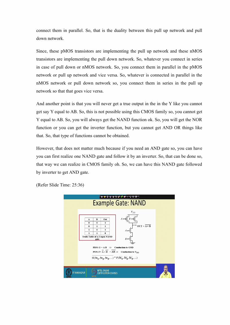
(Refer Slide Time: 25:36)

So, how do we realize the NAND gate? So, here is a here is an example. So, you see
suppose I have got this is a NAND truth table 0 0 1 0 1 1 1 0 0 and 1 1 0 first. So, this is
the corresponding circuitry as I was telling so, there will be a pull down network
consisting of nMOS transistors and there will be a pull up network cons consisting of the
pMOS transistors. And if you look into these two networks so, they are dual up each
other, like whenever I have got this nMOS transistors in series. So, corresponding pMOS
transistors are in parallel and we will see vice versa. So, if you put these nMOS
transistors in parallel for some circuit requirement so, you have to put the nMOS
transistors in series.
So, let us see the combination that when this A equal to 0 and B equal to 0 output is equal
to 1. How does it happen? So, both of them are equal to 0 means both the p transistors
are ON and both the n transistors are OFF. As a result if you measure the voltage so, you
will see the voltage value equal to V D D.
Similarly, if it is 0 1 so, A transistor so, this is 0 and this is 1, as a result this transistor is
ON and this transistor is OFF. Similarly, this transistor is OFF and B transistor is ON;
however, since these two are in series so, it does not matter. So, there is path from this
output to the ground, but there is a path from V D D to OUT via this A transistor;
because A is equal to 0. So, you get the output as 1.
Similarly, when both the inputs are equal to 1 then both the upper p transistors are OFF
and both the n transistors are ON; as a result there is a current flow path from this output
to these things. So, you get a voltage equal to 0 at this point. So, that way this particular
circuit it can realize it can realize the NAND operation. So, you can so, in general we can
say that this pull up network pull down network is AB and pull up network is A bar B bar
which is AB bar. So, that is conduction to V D D and this is conduction to ground.

(Refer Slide Time: 27:49)
So, we can also realize NOR gate in a diffi in a similar fashion like for NOR gate we
have to do this A and B in the in the pull down network. This A and B they should be
connected in parallel and in the pull up network this is A and B they should be connected
in series. So, whenever it is this is a lower network is in parallel, upper network is in
series and vice versa. So, here we can quickly check that when A and B both are equal to
0 output is equal to 1.
If A and both are B are both are equal to 0, then both the lower transistors are OFF and
both the upper transistors are ON. As a result at this point you get the voltage value equal
to V D D. And if any of, if both of them are equal to 1 then both transistors lower
transistors are ON and both the pMOS transistors are OFF; as a result at this point you
will get a 0 volt, ok.
So, this way we can realize this NAND gate and NOR gate in CMOS family.