digital signal conditioning test instrumentation
TRANSCRIPT
NASATechnicalMemorandum101739
Digital Signal Conditioning for FlightTest InstrumentationGlenn A. Bever
(NASA-TM-IOI739) DIGITAL SIGNAL N91_--2_CflNDITIONING POR FLIGHT TEST INRT_UMENTATIL_N ..........
(NASA) 81 p CSCI O]D __ _Unc!, _L .....
83/05 00026 _ - "
March 1991
NASANational Aeronautics and
__.Space Administration

NASA Technical Memorandum 101739
Digital Signal Conditioning for FlightTest InstrumentationGlenn A. BeverAmes Research Center, Dryden Flight Research Facility, Edwards, California
1991
National Aeronautics andSpace AdministrationAmes Research Center
Dryden Flight Research FacilityEdwards, California 93523-0273

PRECEDING PAGE BLANK NOT FILMED
iii
CONTENTS
SUMMARY 0-1
OBJECTIVE 0-I
NOMENCLATURE 0-1
INTRODUCTION
1.1
1.2
1.3
1-1
Definitions ........................................... 1-1
Sampling in the Analog World ................................. 1-2
1.2.1 Common examples ................................... 1-2
1.2.2 Effects and pitfalls (problem areas) .......................... 1-3Tradeoff Considerations ..................................... 1-3
DIGITAL PROCESSES IN FLIGHT TESTING
2.1
2.2
2.3
2.4
2.5
2--1
Avionics Syslems ....................................... 2-I
Data Acquisition Systems ................................... 2-I
Signal Processing--Conditioning ................................ 2-IHardware Considerations ..................................... 2-I
2.4.1 Technology ...................................... 2-I
2.4.1.I Bipolar IcJgic ................................ 2-2
2.4.1.2 Emitter-coupled logic ............................ 2-2
2.4.1.3 CMOS logic ._..YSZ. ............................. 2-3
2A.I A Logic families compared .......................... 2-32.4.1.5 Problem areas ................................ 2-5
2.4.1.6 Programmable logic devices ......................... 2-5
2.4.1.7 Hybrid circuits ............................... 2-6
2.4.2 Environmental considerations ............................. 2--6
2.4.3 Architecture ...................................... 2-6
Software Considerations .................................... 2-7
2.5.1 Languages ....................................... 2-7
2.5.2 Software development ................................. 2-8
ANALOG-TO-DIGITAL INTERFACE 3-1
3.1 Analog-to-Digital Conversion Techniques ........................... 3-1
3.1.1 Succe_,sive apl_roximation ............................... 3-1
3.1.2 Integration ....................................... 3-1
3.1.3 Multiple comparator (flash) converter ......................... 3-2
3.1.4 Tracking converter ................................... 3-3
3.1.5 Sigma delta converler ................................. 3--4
3.2 Digital-to-Analog Conversion Techniques ........................... 3-5
3.3 Digital-to-Synchro Conversion Techniques ............ .............. 3-6
3.4 Synchro-to-Digital Conversion Techniques .......................... 3-73.5 Conversion Process Considelations .............................. 3-7
3.5.1 Sample andlTold .................................... 3-7
3.5.2 Presample filtering ................................... 3-8
3.5.3 Antialiasing filtering .................................. 3-83.6 Process Error Sources ..................................... 3-10
iv
4
5
6
DIGITAL TRANSDUCERS 4-1
4.1 Transduction Techniques .................................... 4-14.1.1 Coded disks ...................................... 4-1
4.1.2 Variable frequency ................................... 4-2
4.1.3 Pulse techniques .................................... 4-2
4.2 Coding ............................................. 4-2
4.2.1 Progressive codes ................................... 4-2
4.2.2 Nonprogressive codes (Gray) ............................. 4-3
DIGITAL FILTERING
5.1
5.2
5.3
5.4
5.5
5--1
Applications and Guidelines .................................. 5-1Time Domain Filters ...................................... 5-1
5.2.1 Nonrecursive filters .................................. 5-2
5.2.2 Recursive filters .................................... 5-2
5.2.3 Switched capacitor filters ............................... 5-2
Statistical Filtering ....................................... 5-4
Data Compression Filtering .................................. 5-4
Pitfalls (Problem Areas) of Digital Filtering .......................... 5-4
DIGITAL COMMUNICATION 6--1
6.1 Technology Choices ...................................... 6-1
6.1.1 Copper wire ...................................... 6-1
6.1.2 Fiber optics ...................................... 6-1
6.1.3 Telemetry ....................................... 6-2
6.2 Transmission Timing Choices ................................. 6-2
6.2.1 Synchronous ...................................... 6-2
6.2.2 Asynchronous ...................................... 6-2
6.2.3 Isochronous ...................................... 6-3
6.3 Communication Format Choices ................................ 6-3
6.3.1 Serial transfer ..................................... 6-3
6.3.2 Parallel transfer .................................... 6-3
6.4 Data Formats .......................................... 6-4
6.4.1 Timing and synchronization .............................. 6--46.4.2 Error detection and correction ............................. 6--4
6.4.2.1 Parity bit .................................. 6-46.4.2.2 Error correction code ............................ 6-5
6.4.2.3 Cyclic redundancy code ........................... 6-6
6.4.3 Data packet format ................................... 6-6Standard Avionics Data Buses ................................. 6--6
6.5.1 MIL-STD-1553/1773 ................................. 6-6
6.5
6.5.1.1
6.5.1.2
6.5.1.3
6.5.1.4
6.5.1.5
6.5.1.6
6.5.1.7
6.5.1.8
6.5.1.9
6.5.1.10
6.5.2
Terminal types ................................ 6-7Data bus cable ................................ 6-8
Terminal characteristics ........................... 6-9
Data bus operation .............................. 6-9
Word types ................................. 6-10Word formats ................................ 6-10
Bus message formats ............................ 6-11MIL-STD-1553 notices ........................... 6-13
Design tips for MIL-STD-1553 ........................ 6-13MIL-STD- 1773 and STANAG ....................... 6-14
ARINC 419/429/629 .................................. 6-14
V
6.6
6.7
6.8
6.5.2.1 ARINC 419 ................................. 6-14
6.5.2.2 ARINC 429 ................................. 6-15
6.5.2.3 ARINC 629 (DATAC) ............................ 6-19
6.5.3 H009 .......................................... 6-20
General-Purpose Data Buses .................................. 6-216.6.1 RS-232/422/423/449 .................................. 6-21
6.6.2 IEEE 488/HP-IB/IEC 625 ............................... 6-24
6.6.2.1 Bus operation ................................ 6-24
6.6.2.2 Bus application and limitations ....................... 6-256.6.3 Ethernet (IEEE 802.3) ................................. 6--25
Sampling Data Buses for PCM Transmission ......................... 6-26
Wave Shaping for Special Situations .............................. 6-27
6.8.1 Pulse trains for telemetry transmission ......................... 6-27
6.8.2 Pulse trains for tape recording ............................. 6-27
6.8.2.1 Filtering and encoding considerations .................... 6-27
6.8.2.2 Enhancement techniques .......................... 6-28
7 DIGITAL DATA STORAGE
7.1
7.2
7.3
7.4
7-1
Tape Recorders ......................................... 7-1
Semiconductor Memory .................................... 7-1
7.2.1 Random access memory ................................ 7-1
7.2.2 Electrically erasable programmable read only memory ................ 7-2
Bubble Memory ........................................ 7-2Disks .................. _ ........................... 7-2
7.4.1 Magnetic (hard and flexible) .............................. 7-2
7.4.2 Optical ......................................... 7-3
7.4.3 Interfacing ....................................... 7-3
TESTING 8--1
8.1 Failure Modes and Mechanisms of Digital Systems ...................... 8-18.2 Hardware Test Methods .................................... 8-1
8.3 Software Test Methods ..................................... 8-2
RELIABILITY AND SAFETY 9-1
9.1 Verification and Validation ................................... 9-1
9.2 Flight-Critical System Data Extraction ............................. 9-1
REFERENCES R-I
INDEX I-1

DIGITAL SIGNAL CONDITIONING FOR FLIGHT TEST
Glenn A. Bever
NASA Ames Research Center
Dryden Flight Research FacilityP.O. Box 273
Edwards, California 93523-0273
U.S.A.
SUMMARY
Hight test instrumentation systems are rapidly evolving from what was an all-analog technology into what
will be an almost all-digital art. The development and widespread application of digital processes in data pro-
cessing and reduction make it imperative that the advantages of the digital approach be exploited wherever
appropriate in the flight test process. The areas of signal conditioning and data acquisition offer many oppor-
tunities to use digital techniques to achieve improved performance. For some time, digital techniques have
seen much use in data acquisition systems. More recently, the use of digital computers in airborne systems
has become commonplace, both in data acquisition systems and in the aircraft avionics and control systems.
The computer brings an extensive capability for real-time processing to the onboard systems and, to realize
its full potential, must be appropriately interfaced to the aircraft environment. Often, aircraft avionic digital
systems contain data which are required for conducting the flight test. It becomes necessary to extract the
data from the onboard systems for inclusion in the flight test database. For these reasons it is essential that
the flight test instrumentation engineer understand digital signal conditioning techniques and be familiar with
their applications.
OBJECTIVE
The objective of this volume is to provide the engineer with a limited theoretical basis, and with the necessary
practical design information to permit the exploitation of the advances in the digital systems state of the art as
applied to flight testing. Included in this objective is the use of digital techniques in strictly signal conditioning
applications as well as interfacing and communication applications between various aircraft systems. Not
included in this objective is the coverage of strictly computer-based systems information. This information is
covered in computer society literature or in software professional society publications. These topics may be
noted for consideration, but the reader is directed to other references for detailed subject coverage.
NOMENCLATURE
AC
ACT
A-D
ALS
AM
AND
ANSI
ARINC
ASCII
alternating current or advanced CMOS
advanced CMOS 'ITL level
analog to digital
advanced low-power Schottky
amplitude modulation
logic "and" function
American National Standards Institute
Aeronautical Radio, Inc.
American Standard Code for Information Interchange
0-2
BC
BCD
Bltl, -L
BM
BNR
CCITT
CMOS
CRC
D-A
DAC
DATAC
DC
DCE
DCTL
DEEC
DITS
DM-M
DoD
DTE
DTL
ECC
ECL
EEPROM
EFA
EMI
EPLD
ESDI
ESD
EU
FAST
FET
FIFO
FIR
FM
FH
bus controller
binary-coded decimal
Manchester II biphase-level
bus monitor
binary
The International Telegraph and Telephone Consultative Committee
complementary metal oxide semiconductor
cyclic redundancy code
digital to analog
digital-to-analog converter
digital autonomous terminal access communication
direct current
data communication equipment
direct-coupled-transistor logic
digital electronic engine control
digital information transfer system
delay modulation-mark (Miller)
Department of Defense (U.S.A.)
data terminal equipment
diode-transistor logic
error correction code
emitter-coupled logic
electrically erasable programmable read-only memory
(also known as E 2 PROM)
European fighter aircraft
electromagnetic interference
electrically programmable logic device
enhanced small device interface
electrostatic discharge
engineering units
Fairchild advanced Schottky TTL
field effect transistor
first in, first out
finite impulse response
frequency modulation
flight test instrumentation
GP-IB
HC
HCT
HP-IB
IC
IEC
IEEE
IIR
IRIG
IRU
ISO
LS
LSB
LSD
LSI
MIL-STD
MODEM
MOS
MSB
MSCP
MSD
NASA
NRZ
PAL
PCM
PLA
PLD
R
RAM
RC
RF
RH
RL
RMI
RT
RTL
general-purposeinterfacebus
high-speedCMOS
high-speedCMOSTI'L level
Hewlett-Packardinterfacebus
integratedcircuit(chip)
InternationalElectrotechnicalCommission
Instituteof ElectricalandElectronicEngineers
infiniteimpulseresponse
Inter-RangeInstrumentationGroup(U.S.A.)inertialreferenceunit
InternationalStandardsOrganization
low-power Schottky
least significant bit
least significant digit
large-scale integration
military standard
modulator-demodulator
metal oxide semiconductor
most significant bit
mass storage control protocol
most significant digit
National Aeronautics and Space Administration (U.S.A.)
nonreturn to zero
programmable array logic
pulse-code modulation
programmable logic array
programmable logic device
resistance
random access memory
resistance-capacitance
radio frequency
rotor reference high
rotor reference low
radio magnetic indicator
remote terminal
resistor-transistor logic
0-3
O--4
RZ
rms
rpm
rps
SAE
SCSI
SDI
SDLC
SM
SSI
SSM
ST506
T/R
TrL
UV
V
VAC
VDT
WORM
return to zero
root mean square
revolutions per minute
revolutions per second
Society of Automotive Engineers
small computer systems interface
source designation indicator
synchronous data link control
status matrix
small-scale integration
sign-status matrix
Seagate disk interface standard
transmit-receive
transistor-transistor logic (bipolar)
ultraviolet
volts
volts alternating current
video display terminal
write once, read many
Symbols
C
D
E
f
I
H
k, m) n
P
O.
R
S
T
Z
capacitor
digital output
electromotive force (voltage)
frequency
current
matrix
variables
parity
charge
ratio
signal
time between successive closings
impedance
ohms
0--5
Subscripts
a_e
clk
G
H
IH
IL
in
n
0
OH
OL
out
pl
pu
ref
8
sl
8U
average
clock
ground
high
input high
input low
input
variable
characteristic or nominal
output high
output low
output
passband lower
passband upper
reference
SOUrCe
stopband lower
stopband upper

1-1
1 INTRODUCTION
Traditionally, engineering disciplines surrounding flight test have been broken into several groups. Groups
concerned with flight operations, flight control, aerodynamics, propulsion, and instrumentation existed with a
great deal of autonomy. More recently, aircraft are being viewed and tested as a complete aircraft SYSTEM.
The dividing lines between disciplines have become very indistinct. Information about fuel distribution may be
input to control systems that adjust for center of gravity change. Digitally controlled propulsion systems may
integrate their calculations with the flight control system. System designers require data from these systems
to evaluate their performance or safety. Instrumentation engineers are taking advantage of sensors embedded
into avionics packages rather than installing their own unique sensors.
More demanding requirements are driving aircraft systems to be more integrated. Many processes traditionally
done on the ground are moving into aircraft systems. Improving digital electronic technology is making aircraft
systems possible that were impossible just a few years ago. Optical technologies loom on the horizon. The
rapid progress in the state of the art requires individuals charged with designing aircraft measuring systems to
become better acquainted with new solutions to their requirements.
This volume is concerned with aircraft measuring systems as related to flight test and flight research. Measure-
merits that are digital in origin or that must be digitized are discussed. Sampling, encoding, transmitting, and
storing the data are dealt with. Examples of actual solutions to these problems will be given. This volume will
provide an overview and introduction to the various areas of concern in modern aircraft digital measurement.
Processes taking place on the aircraft rather than on the ground are emphasized.
There is no one right way to instrument an aircraft. Different organizations have different goals and require-
ments. An aircraft manufacturer has a different emphasis than an organization concerned with basic aerody-
namic research. The manufacturer's primary concern is to validate the aircraft design and to prove its safety.
While a military flight testing organization may be more concerned with gaining experience in a particular air-
craft to write flight manuals, a flight research organization may be more concerned with measuring the airflow
over a wing or doing precise wind calculations. Some organizations can design in the test instrumentation
when the aircraft is built. Others are faced with the task of installing equipment in places that the designers
never envisioned.
For example, designers of avionics systems in civil transport aircraft proceed from a rigid criteria for avionics
box size and function. The designer of flight test instrumentation for fighter or small civil planes is more likely
to use criteria "as small as is practicable" with a function uniquely defined by the flight test program.
The organizations' diverse missions, together with the natural tendency to continue with familiar approaches
to problems and equipment, create a wide range of solutions to flight measurement problems.
1.1 Definitions
What parameters are measured in flight that are of concern to digital signal conditioning? Nearly all parameters
in modern flight test eventually become digital. Even analog sensors are digitized for inclusion into databases
at some point. Avionic systems communicate by way of digital data buses. And increasingly, data is being
digitally stored in memory, tape, and disk. The following basic terms found in this volume are defined.
A measurand is the physical quantity to be measured, such as temperature, pressure, or strain.
A transducer is a device that converts a mea'surand into another form of energy. For flight test instrumentation,
this energy is typically electrical or optical.
Signal conditioning is necessary to convert a transducer output to a form required for input to a recorder,
computer, or telemetry device.
Digital signal conditioning is defined as converting a transducer output signal to the digital domain and passing
it to a recording, computing, or telemetry device. Conditioning or altering signals between different forms in
the analog domain is not discussed in this volume. See reference 1 for a discussion of this topic.
1-2
1.2 Sampling in the Analog World
The adage "to measure is to change" sums up the skill required to measure phenomena. The problem is
twofold. First, probing a medium disturbs it. Second, no measuring device is perfect. Correct interpretation ofhow much the medium has been disturbed and how much error that contributes along with sensor imperfection
is the key to correct interpretation of the results.
When a conversion is made, whether between human languages or between analog and digital, something is lost
in the translation. It is a truism that because it has been changed, it is different. The advantage of handling data
in the digital regime is that it is much less sensitive to further degradation than is a signal in the analog domain.
Because a digital signal is passed as a two-state value, wide tolerances in the signal levels can be accepted and
still retain the information (fig. l-l(a)). However, most measurands of interest are more appropriately thought
of as being in the analog domain (signal amplitude varies with time). Figure 1-1(b) shows a sample analog
signal. Most measurands vary in small amounts, not large (digital)jumps. The problem, then, becomes one of
translating analog phenomena into a digital signal while keeping introduced error to a known minimum.
:::::::::::::::::::::::::::::::::::::::::::::::::::::::::::::::::I I/ Wi! :_:i:i'y2"_'::'::::!''::_:i:::_::_':_':i_i:''_:: ': ::!_:..':._$_::_:!:'::!i"!i_ii_ii_::::::¢:::_. .
_:__ .._:.:.:.:._:.:.:.:.:.:._:.._.:_:.:$_:,%:.:._-:. .__1o76aa 910764b
(a) Digital signal tolerance. (b) Analog signal.
Figure 1-1. Digital and analog signals.
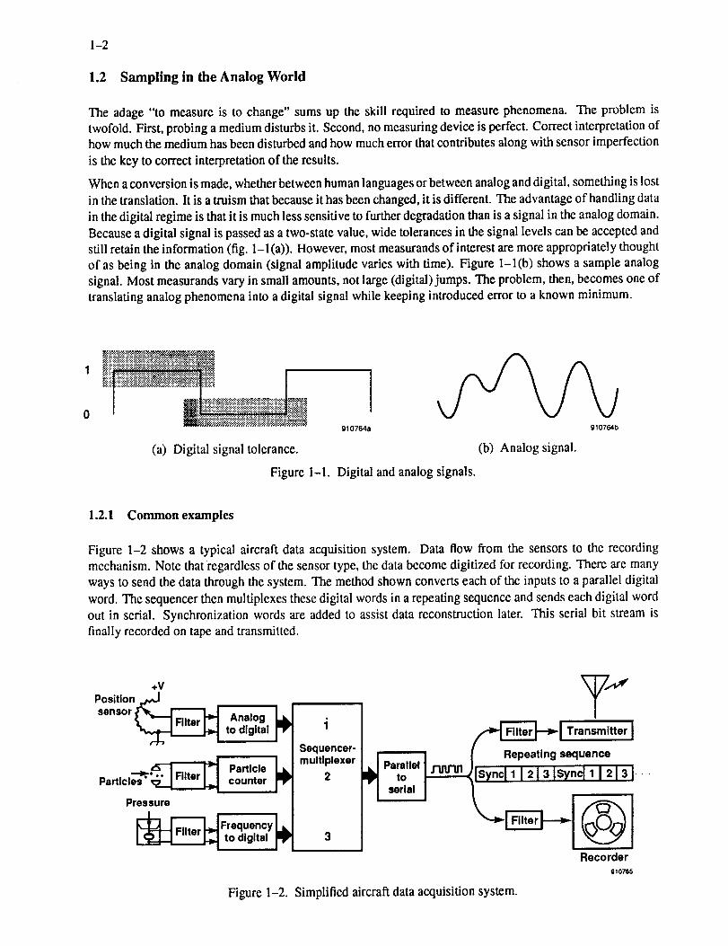
1.2.1 Common examples
Figure 1-2 shows a typical aircraft data acquisition system. Data flow from the sensors to the recording
mechanism. Note that regardless of the sensor type, the data become digitized for recording. There are many
ways to send the data through the system. The method shown converts each of the inputs to a parallel digital
word. The sequencer then multiplexes these digital words in a repeating sequence and sends each digital word
out in serial. Synchronization words are added to assist data reconstruction later. This serial bit stream is
finally recorded on tape and transmitted.
+V
Positionj_
sensor _ toA_lglOtgal_1_
"_ ParticleParticles" counter
Pressure
_Frequencyto digital _l
Sequencer-
multiplexer2
3
i_ Parallel I J'U1J'M'I
1Transmitter J
Repeating sequence,/ISyncl 11 =i IsynclI I I
Recorder10765
Figure 1"2. Simplified aircraft data acquisition system.
1-3
1.2.2 Effects and pitfalls (problem areas)
Sampling introduces its own problems. Sampling is looking at a signal at discrete moments in time. The
more the signal is looked at, the more the sampling rate increases. In theory, as the sampling rate approaches
infinity, the original signal is seen, with no error introduced in sampling. However, in reality the signal must
be sampled less than infinitely often. Sampling circuit limitations, as well as limitations in ability to process,
transmit, or record high data rates, force decisions about how fast the signal must be sampled. If the sampling
rate is too low, important information can be lost. Sampling too high wastes bandwidth resources.
Consider an 8-Hz signal sampled only once. The reconstructed signal will look like a DC level whose amplitude
is whatever the signal happened to be when it was sampled that one time. This is an extreme example of a
phenomena known as aliasing and is discussed in section 3.5.3.
1.3 Tradeoff Considerations
While sampled data systems can lose important information if sampled too low, there are other factors that can
lead to loss of data. Filtering techniques employed to assure that aliasing does not occur must be applied BE-
FORE sampling (sec. 3.5.3). Electronic filtering cannot be used, for example, where scanning pressure trans-
ducers are used. The only antialiasing filtering that can be done here is in the mechanics of the pressure lines.
Techniques other than sampled systems can be subject to the same deficiencies. Systems like FM
recording--where an analog voltage modulates a frequency around a carrier center--are thought to be "con-
tinuous." However, an FM signal cannot be demodulated at one discrete point in time. It takes at least two
points, usually two zero crossings, to determine the frequency AT that time. This implies that arbitrarily large
input variations (continuous signals) cannot be supported because of the finite time it takes to demodulate a
particular frequency. Instantaneous determination of frequency at infinite resolution is required to actually
support a continuous analog input. This is analogous to saying that the system must have an infinite number
of samples to be truly a continuous reading, which is impossible. Everything has a bandwidth, although some
bandwidths are larger than others. Because the carrier is centered at a particular finite frequency and doesn't
have an infinite modulation rate, the ability of the carrier to "carry" information could be exceeded.
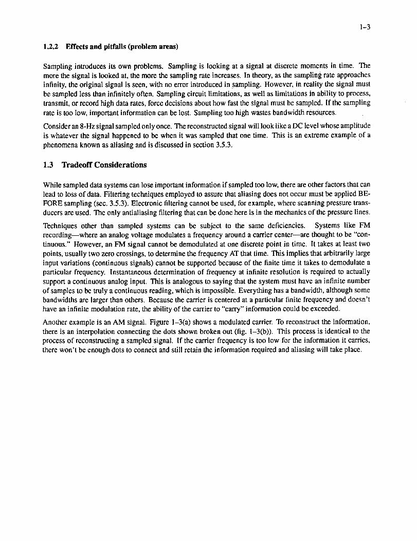
Another example is an AM signal. Figure 1-3(a) shows a modulated carder. To reconstruct the information,
there is an interpolation connecting the dots shown broken out (fig. 1-3(b)). This process is identical to the
process of reconstructing a sampled signal. If the carder frequency is too low for the information it carries,
there won't be enough dots to connect and still retain the information required and aliasing will take place.
1-4
g10766a
(a) Amplitude-modulated waveform. (b) Demodulated waveform, sampled.
Figure 1-3. Sampling nature of amplitude modulation.
910766b
2-1
2 DIGITAL PROCESSES IN FLIGHT TESTING
2.1 Avionics Systems
The word "avionics" is a contraction of the words "aviation" and "electronics," and it may include all elec-
tronic subsystems on an aircraft. In particular, avionics refers to those electronic subsystems that are directly
concerned with flight control, weapon systems, navigation, and cockpit display. In most aircraft, these sys-
tems are part of the operational aircraft, and modifications to these systems are not regarded lightly. They are
designed to exacting specifications, and packaged to facilitate easy replacement by nonexperts.
Avionics systems, as defined previously, are not the subject of this AGARDograph. See reference 2 for more
information on avionics systems. However, because flight testing frequently requires their data, some avioniccommunication standards are discussed in section 6.
2.2 Data Acquisition Systems
Flight testing requirements usually have different ground rules than avionics systems, as defined earlier. Easy
replacement of data acquisition equipment is, of course, desirable. But more important is how flexible the
system is, how easy it is to alter (to test other flight conditions), and how small it is. Data acquisition tradi-
tionally is open loop; that is, data are acquired and stored or transmitted for analysis, but not fed back into the
aircraft to control it. A test display may be available to the pilot, but this isseidom a display certified for safe
flight reference.
2.3 Signal Processing-Conditioning
Referring back to figure 1-2, notice that three different types of sensors are shown. The position sensor, which
may measure control surface position, is a potentiometer whose voltage output varies proportionally with wiper
position. This analog output must be converted to a digital word. The particle sensor must convert individual
particle detection to an aggregate total number of particles detected. The pressure sensor output is a frequency
that is proportional to the pressure applied. This frequency must also be converted to a digital value for use in
the data acquisition system.
Some sensors are regarded as "digital" sensors because the conversion to the digital domain (conditioning) is
done at the sensor. For example, if the only output from the "sensor" box is digital, then it is transparent to the
engineer using it that the pressure sensor is an element of a tuned circuit (the output of which is frequency).
Once the initial "conditioning" to the digital domain is done, then the data must be finally passed to some
recording mechanism. This may mean that the data need to be further conditioned to ease their transfer. For
instance, again referring to figure 1-2, the data are multiplexed, converted to serial (changing their condition
again), and then perhaps filtered (further conditioned) for telemetry transmission or onboard recording. The
data may be used onboard in computations for cockpit displays or data thinning. This type of signal processing
is increasingly common. The conversions and filtering are performed on the digital data to ease their transfer
and in no way alter the basic digital information content.
2.4 Hardware Considerations
2.4.1 Technology
Improvement of electronic technology has proceeded at an incredible rate. It is difficult to maintain an aware-
ness, much less a proficiency, in every development that enters commercial production. Generally, an elec-
tronic designer working against a deadline will design with the familiar. Taking the time to learn the ins and
2-2
outsof anewtechnologyisaluxurythatfrequentlycannotbeindulgedin.Oftennewtechniquesmustbeused,particularlywhenrequirementsdictatelowerpower,higherspeeds,andsmallerpackagesizethanwhatcanbeprovidedwithknowntechniques.
Thedesignengineeroftenneedstohaveexperiencewithnewtechnologyandtechniquesbeforerecommendingit. Therearetoo manyunknownsto makeafirm commitmentto schedule.Techniqueadvancementthenrequiresafar-sightedprojectmanagerorarisk-takingdesignengineerwillingtospendlonghoursperfectingtheunderstandingof thetechniqueinquestion.
Therearecurrentlyseveraltechnologiestochoosefromwhenselectingcomponentstoimplementdigitallogiccircuits.Detailsof thesedevicesarefoundin manufacturers'databooks(refs.3 through7). Reference8discussestechnologyfamilytradeoffs.Thebasictradeoffsmadein selectinga logic familyarepowercon-sumption,gatespeed,noiseimmunity,circuitdensity,outputdrive(fan-out),cost,andreliability.
2.4.1.1 Bipolar logic
This line of logic components is the first line of digital integrated circuits to come into commercial usage. The
technique uses bipolar transistors. Historically, the order of development and usage was:
Direct-coupled-transistor logic (DCTL)
Resistor-transistor logic (RTL)
Diode-transistor logic (DTL)
Transistor-transistor logic (TIL)
A DCTL device had poor noise immunity and high current consumption. An RTL device was low speed, and
had poor noise immunity and low fan-out. A DTL device reduced power requirements, but at the expense of
being slower. All of these technologies are obsolete and are not used in new designs.
The TTL devices have been by far the most popular logic family for nearly 20 years. This logic, or variations
of it, can still be found in new designs, although its popularity is waning. It boasts higher noise immunity than
its predecessors and is fastei'. Subfamilies of TTL have been introduced to improve various characteristics, like
lower power consumption or higher speed. A commercial logic-integrated circuit (IC) is easily recognized by
its prefix of 74. A military specification IC prefix is generally 54. The subfamilies follow the prefix with letters
indicating the subfamily, as follows:
AS
ALS
H
L
LS
S
Advanced Schottky
Advanced low-power Schottky
High speed (up to 50 MHz)
Low power (up to 3 MHz)
Low-power Schottky (up to 45 MHz)
Schottky (up to 125 MHz)
Bipolar logic families are inherently current devices, because bipolar junction transistors are current driven.
Therefore, output drive is limited to some finite number, usually stated in terms of how many logic inputs
(in the samelogic family) can be fed before the current demand moves the output voltage into the transition
(indeterminate) region. This unit of drive capability is called the fan-out. Fan-out for TIL devices is usually
around 10. Switching speeds are regarded as fast because of the use of transistors rather than passive resistor-
capacitor coupling between most stages.
2.4.1.2 Emitter-coupled logic
Emitter-coupled logic (ECL) is characterized by extremely high speeds, into the 1- to 2-GHz range. The
tradeoff is that it also has high power consumption and low circuit density. The ECL operates in the active
region of the transistor--which enhances its speed. The high power consumption and low circuit density limit
its use on aircraft. It is seen primarily in mainframe computers.
2-3
2.4.1.3 CMOS logic
Complementary metal oxide semiconductor (CMOS) logic circuits are voltage driven rather than current driven
as bipolar circuits are. They are voltage driven because CMOS uses field effect transistors (FET's), which are
voltage-driven devices. This is what allows for the low power consumption of CMOS devices. With a constant
voltage and low current leakage, power dissipations in the microwatts can be achieved. Voltage-driven gates
also allow for much larger fan-outs than can be achieved with bipolar devices.
The CMOS device has existed for several years in the form of the 4000 series parts. It boasts high noise
immunity and extremely low power consumption, which has made it popular for battery-operated equipment.
However, 4000 series CMOS is very slow when compared with the bipolar logic families (fig. 2-1).
As technology has progressed, other CMOS logic families have been developed to be plug replaceable with
existing bipolar logic families. For example, the 54HCI74HC family was designed to replace the 54LS/74LS
bipolar family. It retains much of the bipolar speed but reduces the power consumption while improving noise
immunity characteristic of CMOS. Later, the 54AC/74AC family was designed to replace the 54HC/74HC
family while increasing the speed.
2.4.1.4 Logic families compared
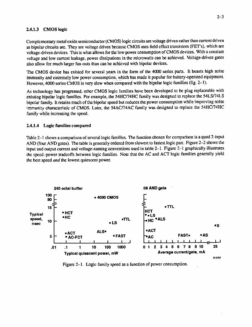
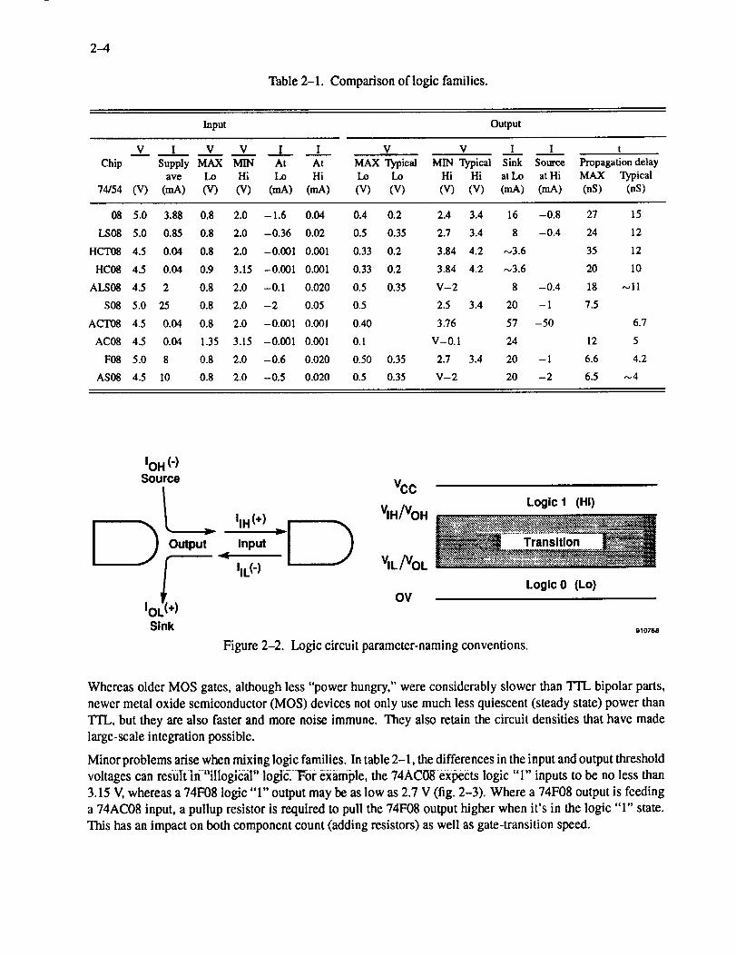
Table 2-1 shows a comparison of several logic families. The function chosen for comparison is a quad 2-input
AND (four AND gates). The table is generally ordered from slowest to fastest logic part. Figure 2-2 shows the
input and output current and voltage-naming conventions used in table 2-1. Figure 2-1 graphically illustrates
the speed-power tradeoffs between logic families. Note that the AC and ACT logic families generally yield
the best speed and the lowest quiescent power.
Typicalspeed,
nsec
10080
15"
10
240 octal buffer 08 AND gate
i
.01
• HCTeHC
• 4000 CMOS
• LS,TrL
i
m
-" eTTLHCTeeLS-eriC eALS
• ACT ALS• •ACT• AC-FCT * FAST -"AC FAST• • ASI I I I I I [ I I ! I I I i ! i
.1 1 10 100 1000 0 1 2 3 4 5 6 7 8 9 10
Typical quiescent power, mW Average currant/gate, mA
Figure 2-1. Logic family speed as a function of power consumption.
eS
25
910787
2-4
Table 2-1. Comparison of logic families.
Chip
74/54
Input Output
V I V V I I V V I I
(V)
Supply MAX MIN At At MAX Typical MIN l"_ypical Sink Sourceave Lo Hi Lo Hi Lo Lo Hi Hi at Lo at Hi
(mA) (V) (V) (mA) (mA) (V) (V) (V) (V) (mA) (mA)
Propagation delay
MAX Typical
(nS) (nS)
O8
LS08
HCT08
HC08
ALS08
S08
ACT08
AC08
F08
AS08
5.0 3.88 0.8 2.0 - 1.6 0.04 0.4 0.2 2_4 3.4 16 -0.8
5.0 0.85 0.8 2.0 -0.36 0.02 0.5 0.35 2.7 3.4 8 -0.4
4.5 0.04 0.8 2.0 -0.001 0.00l 0.33 0.2 3.84 4.2 ,,,3.6
4.5 0.04 0.9 3.15 -0.001 0.001 0.33 0.2 3.84 4.2 _3.6
4.5 2 0.8 2.0 -0.1 0.020 0.5 0.35 V-2 8 -0.4
5.0 25 0.8 2.0 -2 0.05 0.5 2.5 3.4 20 - l
4.5 0.04 0.8 2.0 -0.001 0.001 0.40 3.76 57 -50
4.5 0.04 1.35 3.15 -0.00l 0.001 0.1 V-0.1 24
5.0 8 0.8 2.0 -0.6 0.020 0.50 0.35 2,7 3.4 20 - 1
4.5 10 0.8 2.0 -0.5 0.020 0.5 0.35 V-2 20 -2
27 15
24 12
35 12
20 10
18 ,'-,11
7.5
6.7
12 5
6.6 4.2
6.5 N4
IOH (-)
Source
) )IOL(_+ ) ILL(')
VCC
vi./Vo.
VlL/VoL
OV
Logic I (HI)
1__ _:'._4..., t ........
Logic 0 (Lo)
Sink
Figure 2-2. Logic circuit parameter-naming conventions.
910768
Whereas older MOS gates, although less "power hungry," were considerably slower than TI'L bipolar parts,
newer metal oxide semiconductor (MOS) devices not only use much less quiescent (steady state) power than
"ILL, but they are also faster and more noise immune. They also retain the circuit densities that have made
large-scale integration possible.
Minor problems arise when mixing logic families. In table 2-1, the differences in the input and output threshold
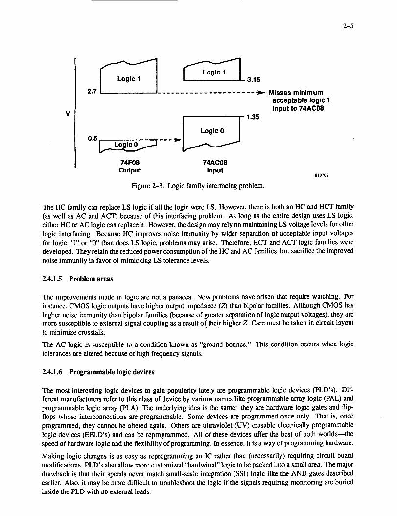
voltages can result in "illogic_ii" logic. For example, the 74AC08 expects logic "1" inputs to be no less than
3.15 V, whereas a 74F08 logic "1" output may be as low as 2.7 V (fig. 2-3). Where a 74F08 output is feeding
a 74AC08 input, a pullup resistor is required to pull the 74F08 output higher when it's in the logic "1" state.
This has an impact on both component count (adding resistors) as well as gate-transition speed.
2-5
V
3.15
..),.
0.5_--- _=.._ 1.35
74F08 74AC08Output Input
Figure 2-3. Logic family interfacing problem.
Misses minimumacceptable logic 1input to 74AC08
910769
The HC family can replace LS logic if all the logic were LS. However, there is both an HC and HCT family
(as well as AC and ACT) because of this interfacing problem. As long as the entire design uses LS logic,
either HC or AC logic can replace it. However, the design may rely on maintaining LS voltage levels for other
logic interfacing. Because HC improves noise immunity by wider separation of acceptable input voltages
for logic 'T' or "0" than does LS logic, problems may arise. Therefore, HCT and ACT logic families were
developed. They retain the reduced power consumption of the HC and AC families, but sacrifice the improved
noise immunity in favor of mimicking LS tolerance levels.
2.4.1.5 Problem areas
The improvements made in logic are not a panacea. New problems have arisen that require watching. For
instance, CMOS logic outputs have higher output impedance (Z) than bipolar families. Although CMOS has
higher noise immunity than bipolar families (because of greater separation of logic output voltages), they are
more susceptible to external signal coupling as a result of their higher Z. Care must be taken in circuit layout
to minimize crosstalk.
The AC logic is susceptible to a condition known as "ground bounce." This condition occurs when logic
tolerances are altered because of high frequency signals.
2.4.1.6 Programmable logic devices
The most interesting logic devices to gain popularity lately are programmable logic devices (PLD's). Dif-
ferent manufacturers refer to this class of device by various names like programmable array logic (PAL) and
programmable logic array (PLA). The underlying idea is the same: they are hardware logic gates and flip-
flops whose interconnections are programmable. Some devices are programmed once only. That is, once
programmed, they cannot be altered again. Others are ultraviolet (UV) erasable electrically programmable
logic devices (EPLD's) and can be reprogrammed. All of these devices offer the best of both worlds--the
speed of hardware logic and the flexibility of programming. In essence, it is a way of programming hardware.
Making logic changes is as easy as reprogramming an IC rather than (necessarily) requiring circuit board
modifications. PLD's also allow more customized "hardwired" logic to be packed into a small area. The major
drawback is that their speeds never match small-scale integration (SSI) logic like the AND gates described
earlier. Also, it may be more difficult to troubleshoot the logic if the signals requiting monitoring are buriedinside the PLD with no external leads.
2-6
2.4.1.7 Hybrid circuits
When it is necessary to miniaturize systems, hybrid circuits may become necessary. Hybrid circuits are a
group of monolithic IC's, resistors, and capacitors that are wired as a circuit. A unique quality of hybrids is
that the IC's are the "chips"--without their carrier package, which saves board space. The hybrid technique
requires manual fabrication, a disadvantage which drives up the cost. Savings of scale are minimal because ofthe manual labor involved.
2.4.2 Environmental considerations
Airborne electronics often encounter a wide range of environments. For example, a fighter aircraft may absorb
tremendous heat sitting on a ramp in the desert. The aircraft then takes off and flies to high altitudes (low
ambient pressure) where ambient temperatures are -50°C, then returns to the hot desert floor. The same
aircraft might be flown from the deck of a damp aircraft carder. The possibility of high electromagnetic
radiation environment operation must be considered as well.
Operational aircraft electronics are designed to withstand all the extremes just listed. This dramatically in-
creases the cost of flight systems as a result of more .difficult design and manufacturing constraints plus
required testing.
Often in flight test, design criteria can be relaxed considerably because the mission ground rules can be more
controlled. In most cases, instrumentation equipment failure results in the termination of data acquisition and
does not endanger the safety of the aircraft. Also, mission rules may dictate operating only in clear weather
when the ramp temperatures are below 30°C. The test instrumentation could be located in a pressurized area
where there is good airflow. These rules would allow the instrumentation to be less expensive and to be
designed more quickly.
Another environmental consideration that is gaining importance is electrostatic discharge (ESD). Static electric
charges build up on the bodies ofpersonnel. An example of electrostatic discharge is the spark generated when
reaching for a doorknob on a dry winter day. The discharge can cause electronic components to be damaged or
destroyed. Less known is that ESD can damage electronic components even when it hasn't built to the level of
discharging a spark. This sensitivity to ESD worsens as IC fabrication technologies shrink IC line widths to fit
more logic on a substrate. Precautions must be taken to prevent damage. Personnel working with electronics
must be grounded through high-impedance leads. High-impedance leads allow a charge to drain off gradually.
If a charge drains instantaneously, high currents would flow or a spark would occur.
2.4.3 Architecture
There are many ways to design a data acquisition system. In most engineering endeavors, compromises must
be made depending on design constraints. For example, constraining a system to be under 1000 cm 3 and less
than 5 kg probably constrains the power dissipation, but not the cost. Optimizing the cost may minimize the
channels available and determine minimum size possible.
As table 2-1 illustrates, modern logic families are becoming faster and dissipate less power than before. The
size of IC components is also shrinking, which means that more electronics per unit area is possible. This in
turn drives up the dissipation requirements. While the units are shrinking, the computational requirements are
increasing. These increased computational requirements can drive an increase in unit size. The usual tradeoff
is size as opposed to performance.
Data acquisition on an aircraft can be categorized into three basic groups: centralized, distributed, and separate.
A centralized data acquisition system has one central controller that directly controls the data acquisition of all
the sensors. It also determines what the output data stream will be. Refer to figure 1-2 for a simplified example.
2-7
A distributed data acquisition system is more loosely coupled. It may be thought of as several "central" data
acquisition systems that share information--usually through digital serial channels. One system directs the
sampling of the rest, but the actual sampling, filtering, and conversion into digital form is done at each remote
location. Distributed systems are important when long lengths of thick wire bundles must be avoided, such as
on large aircraft with widely separated sensors or on small aircraft with no room for wire bundles. "Separate"
data acquisition systems coexist on an aircraft but have nothing to do with each other. This is frequently the
simplest approach but has the disadvantage of not allowing all the aircraft data acquisition to be synchronized.
Although this approach may work for "gross" observation of data, it is frequently intolerable for research.
2.5 Software Considerations
2.5.1 Languages
There was a time when a clear delineation was made between software and hardware. To a software engineer,
hardware was something that software was run on. To a hardware engineer, software was the afterthought of
the hardware buildup process.
With aircraft, if software was needed, it was in assembly language. This was the responsibility of the hardware
engineers. Aircraft systems had to run fast. Programming was viewed as logic replacement, and software wasembedded into the hardware. The fastest way to run code was to program in machine code or its slightly more
human readable form called assembly language.
With the advent of highly digital aircraft, the thought of programming and verifying several interconnecting
digital systems all programmed in assembly language is horrifying. The difficulty in "thinking like a machine"
is increased considerably because of the complexity of several, usually asynchronous, systems. Increased
processing speeds and higher density memories have allowed higher level languages to be considered for
many onboard systems.
A high-level language allows the programmer to write code in a more abstract manner--the programmer's
attention can be spent more on solving the problem than on moving bits around a machineiwhich is where
much of the assembly language programmer's time is spent. The tradeoffis that the programmer has less to dowith the machine level and a certain level of control is lost. With a high-level language, overhead is increased
(taking more time and memory to execute code). But time to code the solution is usually decreased (more time
spent on solving the problem and less time telling the machine how to implement it).
Many high-level languages are in use. Four of the most representative and important languages are FORTRAN,PASCAL, "C," and ADA. The FORTRAN (FORmula TRANslation) language has existed since the 1950's
and is still a very well understood and popular language. It excels at just that--translating formulas ("number
crunching"). In earlier forms it relied on a "threaded code" concept to pass control around a programl This
form is more difficult to follow than the so-called structured program concept used by FORTRAN 77 and the
quintessential model of structured programming, PASCAL.
The PASCAL language was developed to teach students good structured programming concepts. To this end, it
maintains a "death grip" on programming technique. It also separates the programmer from the hardware--by
definition. PASCAL is largely self-documenting. Variables are strongly typed (integer, real number, logical
variable, and so forth), and the use of pointers and record structures allows queues, linked lists, and data
structures to be implemented easily. The main drawback for embedded data system applications like aircraft
avionics is that the real world intrudes on this view of a structured universe and hooks into the hardware must
be provided. Because PASCAL (in standard implementations) is hard to fool, the usual approach is to call
assembly language subroutines to do the hardware access. The programmer will then spend time working
around the program to accomplish the task.
The "C" language was developed at Bell Labs, Murray Hill, New Jersey. Its main purpose was to build op-
erating system elements--UNIX in particular. There are two advantages to this. First, the operating system
2-8
programmercanwrite theoperating system code in a high-level language. Second, the operating system is
more portable between computers because the system programming is written at the abstract level and not at a
machine dependent, assembly language level. But operating systems must deal with the real world of system
input-output (disk read-writes, terminal access, printing, and so forth). The "C" program is less strongly typed
than PASCAL and allows much "bit twiddling," or bit manipulations. In fact, "C" fits in a niche between
assembly code and PASCAL. It includes data structures, block structuring of code, and high-level parsing of
coding, and allows the programmer to bypass much of it. Usually, when high-level language concepts are
bypassed, the code is less portable. Also, "C" language is frequently less readable. As "C" is a very cryptic
language, considerable attention must be paid to making it readable. It is not a self-documenting language.
The most touted and controversial high-level language to come along in recent years is ADA. Unlike "C" or
PASCAL, which came out of development groups and universities and gained acceptance in a "bottom up"
fashion, ADA is advocated by the U.S. Department of Defense (DoD) as a standard language for all coding
done on its programmable systems. The advantage of this standardization is that overall system maintenance
costs are minimized because larger pools of expertise are maintained. The ADA language is designed to be all
things to all people. It developed out of committee (top down) and is a very large compiler. It is so large and so
slow, in fact, that the writing of compilers for different machines and the verification of them is a long process.
By definition no extensions are allowed, so all bases must be covered within the language. The end result is
a language that is too large and too slow for many of the microprocessor-embedded applications (including
logic replacement functions) on board aircraft. However, because DoD is mandating its use, the flight test
community must take ADA seriously.
2.5.2 Software development
Software development, like hardware development, requires a clear definition, a development plan, and a
verification process of the problem to be solved. Tools are needed for writing the code and debugging it. The
time and tools required to debug software are frequently underestimated. "Data crunching" software requires
no interface other than disk drives, a printer, and an operator terminal. Software designed for flight activity
interfaces to many other systems. These systems usually have their own ideas as to when to send and receive
signals, as they are related to real-time processes.
Usually, the code cannot be fully tested until it has been run on the aircraft and connected to the systems
used in flight. Some simulation can be done before this. Software modules can be written to simulate (in a
parameter-passing sense) the aircraft systems. Language debuggers can be used to examine trouble spots in
code execution. But timing checks are very difficult to do without connecting to the aircraft systems. Some-
times code is written on one type of computer and the execution is targeted for another type of computer. This
process is called cross-compilation or cross-assembly, depending on whether a compilation or assembly is
done. Cross-compilation or cross-assembly allows common ground-based computers (designed for general-
purpose use) to be used as a tool in developing code for a system that is optimized as an embedded system.
3-1
3 ANALOG-TO-DIGITAL INTERFACE
3.1 Analog-to-Digital Conversion Techniques
Analog-to-digital (A-D) conversion is central to most data acquisition systems. If a time-varying voltage is
the output of a sensor, and the data will be stored in a digital fashion, it must be converted from the analog
domain to the digital domain. There are several ways to perform this conversion. This section will briefly
describe the methods and the tradeoffs between them.
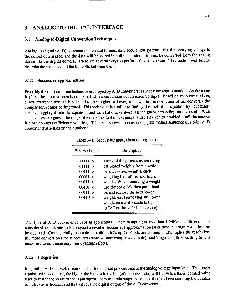
3.1.1 Successive approximation
Probably the most common technique employed by A-D converters is successive approximation. As the name
implies, the input voltage is compared with a succession of reference voltages. Based on each comparison,
a new reference voltage is selected (either higher or lower) until within the resolution of the converter the
comparison cannot be improved. This technique is similar to finding the root of an equation by "guessing"
a root, plugging it into the equation, and then halving or doubling the guess depending on the result. With
each successive guess, the range of excursions to the next guess is itself halved or doubled, until the answer
is close enough (sufficient resolution). Table 3-1 shows a successive approximation sequence of a 5-bit A-Dconverter that settles on the number 6.
Table 3-1. Successive approximation sequence.
Binary Output Description
11111 >
01111 >
00111 >
00011 <
00111 >
00101 <
00111 >
00110 =
Think of the process as removing
calibrated weights from a scale
balance--five weights, each
weighing half of the next higher
weight. When removing a weight
tips the scale (<), then put it backon and remove the next lower
weight, until removing any lower
weight causes the scale to tip
to "<," or the scale balances (=).
This type of A-D converter is used in applications where sampling at less than 1 MHz is sufficient. It is
considered a moderate-to-high-speed converter. Successive approximation takes time, but high resolution can
be obtained. Commercially available monolithic IC's up to 16 bits are common. The higher the resolution,
the more conversion time is required (more voltage comparisons to do), and longer amplifier settling time is
necessary to minimize amplifier dynamic effects.
3.1.2 Integration
Integrating A-D converters count pulses for a period proportional to the analog voltage input level. The longer
a pulse train is counted, the higher the integration value (of the pulse train) will be. When the integrated value
rises to match the value of the input signal, the pulse train stops. A counter that has been counting the number
of pulses now freezes, and this value is the digital output of the A-D converter.
3-2
Dualslopeintegrationinvolvesintegratingtheanalogvoltageinputfor apredeterminedtime. A referenceinputis thenswitchedintotheintegratorandintegrates"down"tozero(whereit started).Thetimeit takesfor thesecond(down)integrationprocessisproportionaltotheaverageof theanaloginputvoltageovertheperiodof thefirstintegration.A digitalpulsetrainpulsesoverthesecond(down)integrationperiodandacounterkeepstrackof thenumberof pulses.Theresultingnumberis thedigitaloutputandis proportionaltotheanaloginputvoltage.Theadvantageof dualslopeoverasingleslopeintegratoris thatthedualslopeincreasesaccuracyandcancelsouttemperatureeffectscontributedbyresistorandcapacitortimeconstants.Itdoesthisattheexpenseof requiringmorecontrollogic.
Forexample,in figure3-1 threesignalsareshown:St, $2, and $3. The S_ signal is the smallest, so it
integrates up to the smallest level in time, Tt. When the reference input is switched in at T1, the counter is
started, and all three signals integrate down at the same rate. The $1 signal reaches zero first (at point C1 ),
where its counter terminates. Obviously, i f the counter terminated at 02, its value would be greater--indicating
that ,5'2 is larger than $1.
Sight_ _al integrate _ ] Reference Integrate
time r I time slope >vc
S3
0
C1 C 2 C 3Fixed
910770
Figure 3-1. Dual slope integration analog-to-digital converter.
Very high resolution data can be obtained at moderate speeds and low cost using this technique. Multiple
integration cycles can improve the resolution and accuracy at the expense of speed. The integration process
reduces noise at frequencies whose periods are shorter than the signal integration time (higher frequencies). A
sample and hold is not necessary.
3.1.3 Multiple comparator (flash) converter
This type of A-D converter is the fastest because the conversion takes place combinationally (unclocked) all
at one time. It does this by using many voltage comparators simultaneously. In a true flash converter, 2 '_- 1
comparators are used, where n equals the number of bits in the A-D output. Each comparator is set for a
diffcrent level and graded in equal divisions from the minimum to maximum acceptable input voltage. All
of the comparators with references below the input voltage will indicate HIGHER and the comparators with
reference voltages above the input voltage will indicate LOWER. It is like reading a thermometer, where the
mercury is seen at each degree below the indicated temperature and no mercury is seen at each degree above
the indicated temperature.
The output of each comparator is fed into a priority encoder that converts the decoded inputs to an encoded
binary output. The priority encoder requires 2"- 1 inputs and n outputs. This process requires many accurate
voltage comparators and gates for the usual case where n _>8. It is very fast, however, because the conversion
happens at once.
3-3
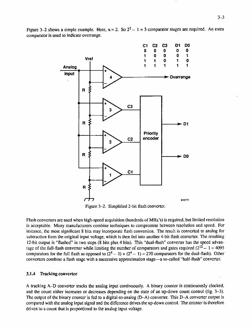
Figure3-2 shows a simple example. Here, n = 2. So 22- 1 = 3 comparator stages are required. An extra
comparator is used to indicate overrange.
Vref
Analog
input
Cl C2 C3 D1 DO0 0 0 0 01 0 0 0 11 1 0 1 01 1 1 1 1
Overrange
C3
C2
Cl
Priorityencoder
Figure 3-2. Simplified 2-bit flash converter.
D1
DO
910771
Flash converters are used when high-speed acquisition (hundreds of MHz's) is required, but limited resolution
is acceptable. Many manufacturers combine techniques to compromise between resolution and speed. For
instance, the most significant 8 bits may incorporate flash conversion. The result is converted to analog for
subtraction from the original input voltage, which is then fed into another 4-bit flash converter. The resulting
12-bit output is "flashed" in two steps (8 bits plus 4 bits). This "dual-flash" converter has the speed advan-
tage of the full-flash converter while limiting the number of comparators and gates required (212 - 1 = 4095
comparators for the full flash as opposed to (28- 1) + (24 - 1) = 270 comparators for the dual-flash). Other
converters combine a flash stage with a successive approximation stage--a so-called "half-flash" converter.
3.1.4 Tracking converter
A tracking A-D converter tracks the analog input continuously. A binary counter is continuously clocked,
and the count either increases or decreases depending on the state of an up-down count control (fig. 3-3).
The output of the binary counter is fed to a digital-to-analog (D-A) converter. This D-A converter output is
compared with the analog input signal and the difference drives the up-down control. The counter is therefore
driven to a count that is proportional to the analog input voltage.
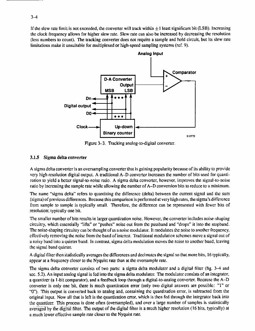
3-4
If theslewratelimit is not exceeded, the converter will track within + 1 least significant bit (LSB). Increasing
the clock frequency allows for higher slew rate. Slew rate can also be increased by decreasing the resolution
(less numbers to count). The tracking converter does not require a sample and hold circuit, but its slew rate
limitations make it unsuitable for multiplexed or high-speed sampling systems (ref. 9).
Analog input
D-A Converter l
Output IMSB LSB I
Dn__. iTeeeI IDigital outputI I 1
DO_ II0°'il
Clock--_ Up-down I '_Binary counter910772
Figure 3-3. Tracking analog-to-digital converter.
3.1.5 Sigma delta converter
A sigma delta converter is an oversampling converter that is gaining popularity because of its ability to provide
very high resolution digital output. A traditional A-D converter increases the number of bits used for quanti-
zation to yield a better signal-to-noise ratio. A sigma delta converter, however, improves the signal-to-noise
ratio by increasing the sample rate while allowing the number of A-D conversion bits to reduce to a minimum.
The name "sigma delta" refers to quantizing the difference (delta) between the current signal and the sum
(sigma) of previous differences. Because this comparison is performed at very high rates, the sigma's difference
from sample to sample is typically small. Therefore, the difference can be represented with fewer bits of
resolution; typically one bit.
The smaller number of bits results in larger quantization noise. However, the converter includes noise-shaping
circuitry, which essentially "lifts" or "pushes" noise out from the passband and "drops" it into the stopband.
The noise-shaping circuitry can be thought of as a noise modulator. It modulates the noise to another frequency,
effectively removing the noise from the band of interest. Traditional modulation schemes move a signal out of
a noisy band into a quieter band. In contrast, sigma delta modulation moves the noise to another band, leaving
the signal band quieter.
A digital filter then statistically averages the differences and decimates the signal so that more bits, 16 typically,
appear at a frequency closer to the Nyquist rate than at the oversample rate.
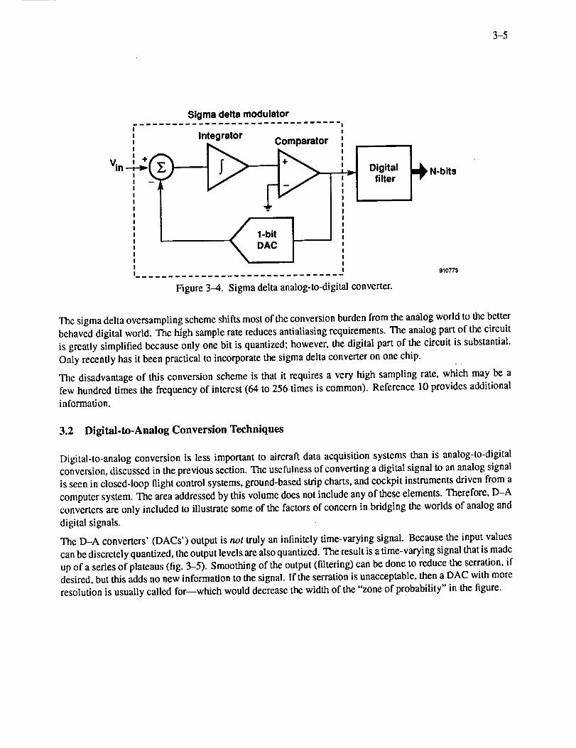
The sigma delta converter consists of two parts: a sigma delta modulator and a digital filter (fig. 3--4 and
sec. 5.2). An input analog signal is fed into the sigma delta modulator. The modulator consists of an integrator,
a quantizer (a 1-bit comparator), and a feedback loop through a digital-to-analog converter. Because the A-D
converter is only one bit, there is much quantization error (only two digital answers are possible: "1" or
"0"). This output is converted back to analog and, containing the quantization error, is subtracted from the
original input. Now all that is left is the quantization error, which is then fed through the integrator back into
the quantizer. This process is done often (oversampled), and over a large number of samples is statistically
averaged by the digital filter. The output of the digital filter is a much higher resolution (16 bits, typically) at
a much lower effective sample rate closer to the Nyquist rate.
3-5
Sigma delta modulator
III
Vin _--_. '
Integrator Comparator
Figure 3--4. Sigma delta analog-to-digital converter.
910773
The sigma delta oversampling scheme shifts most of the conversion burden from the analog world to the better
behaved digital world. The high sample rate reduces antialiasing requirements. The analog part of the circuit
is greatly simplified because only one bit is quantized; however, the digital part of the circuit is substantial.
Only recently has it been practical to incorporate the sigma delta converter on one chip.
The disadvantage of this conversion scheme is that it requires a very high sampling rate, which may be a
few hundred times the frequency of interest (64 to 256 times is common). Reference 10 provides additionalinformation.
3.2 Digital-to-Analog Conversion Techniques
Digital-to-analog conversion is less important to aircraft data acquisition systems than is analog-to-digital
conversion, discussed in the previous section. The usefulness of converting a digital signal to an analog signal
is seen in closed-loop flight control systems, ground-based strip charts, and cockpit instruments driven from a
computer system. The area addressed by this volume does not include any of these elements. Therefore, D-A
converters are only included to illustrate some of the factors of concern in bridging the worlds of analog and
digital signals.
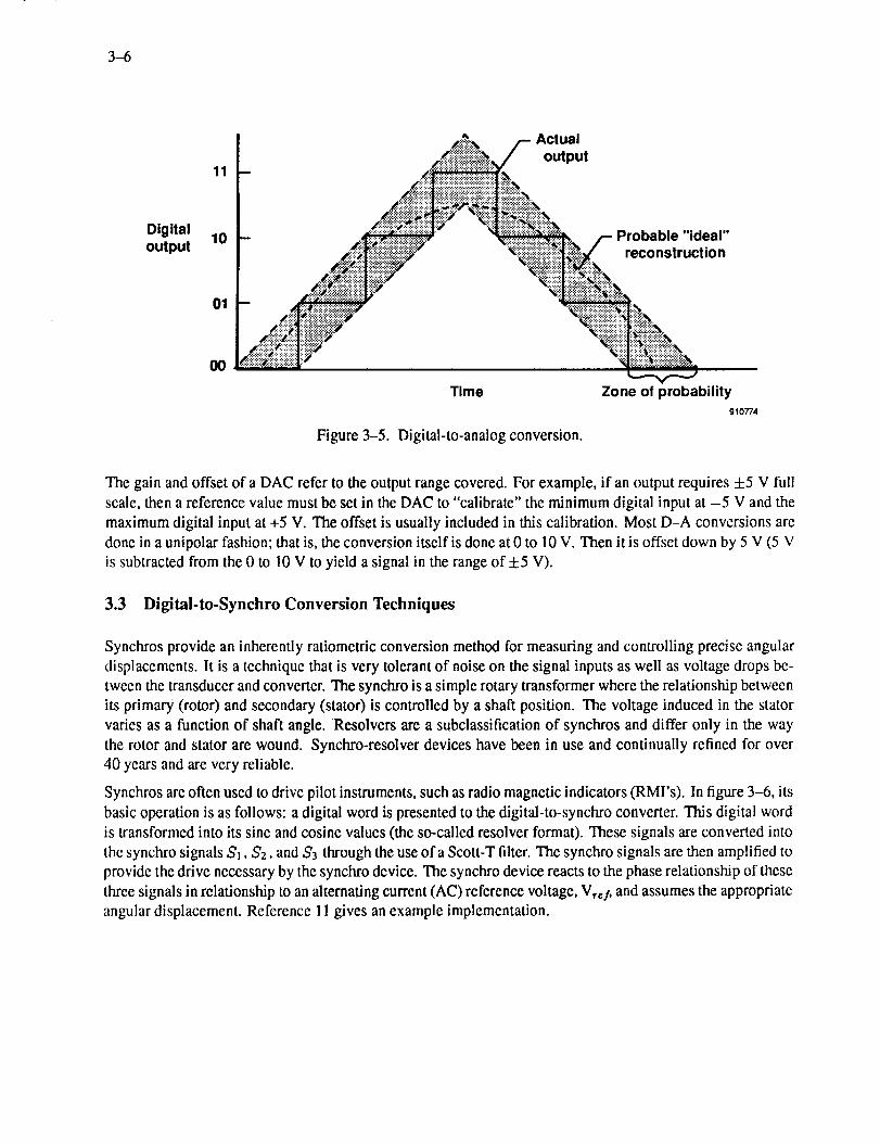
The D-A converters' (DACs') output is not truly an infinitely time-varying signal. Because the input values
can be discretely quantized, the output levels are also quantized. The result is a time-varying signal that is made
up of a series of plateaus (fig. 3-5). Smoothing of the output (filtering) can be done to reduce the serration, if
desired, but this adds no new information to the signal. If the serration is unacceptable, then a DAC with more
resolution is usually called for--which would decrease the width of the "zone of Probability" in the figure.
3-6
I ./.:::_:_ /-- Actual
/ output11 _ _iii_ii__:i ' ::_
I _i_i_::_i_i::]iii7::i_i_!:7ii_i_i7_:,::]!ii_:_:--_i_!::!:_:_:!:.:_:_!:::::!'"..:_i_:_'' _;:_:i:_:i:::.i_::'::::_:_:_ii:!:i:i_
Dig itaI -- _:_. ....... _.,_:.:_.:!:i:_:i:_.:_:_:_._._.Pr^"- " I^ "i" ^- I"output 10 F #..__ _"_i_i_ii_..:]-i::_iii::;::iI_}_freconstruction
01 _'_, .i:V":.::i:i:::_::::'-'.::_:-::5:i:V: :_!!._!:_:!:__N_i:-i:i_i!::.";_i_ ]iii::!_i::ii!iii_i_i._i_.:!.-'-%::_
_ -_'::_:-:::::::::_-_[:i_:.-"i-:_._7!_!._iiiiiii_;' _i_:_:_:_:_::::::::::::::::::::::::::::::::::::::::::::::: :::::_- _:::::: ::::::::::::::::::::::::::::::::::
Time Zone of probability910774
Figure 3-5. Digital-to-analog conversion.
The gain and offset of a DAC refer to the output range covered. For example, if an output requires +5 V full
scale, then a reference value must be set in the DAC to "calibrate" the minimum digital input at -5 V and the
maximum digital input at +5 V. The offset is usually included in this calibration. Most D-A conversions are
done in a unipolar fashion; that is, the conversion itself is done at0 to 10 V. Then it is offset down by 5 V (5 V
is subtracted from the 0 to 10 V to yield a signal in the range of +5 V).
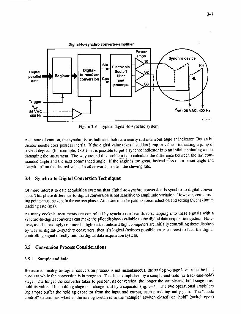
3.3 Digital-to-Synchro Conversion Techniques
Synchros provide an inherently ratiometric conversion method for measuring and controlling precise angular
displacements. It is a technique that is very tolerant of noise on the signal inputs as well as voltage drops be-
tween the transducer and converter. The synchro is a simple rotary transformer where the relationship between
its primary (rotor) and secondary (stator) is controlled by a shaft position. The voltage induced in the stator
varies as a function of shaft angle. Resolvers are a subclassification of synchros and differ only in the way
the rotor and stator are wound. Synchro-resolver devices have been in use and continually refined for over
40 years and are very reliable.
Synchros are often used to drive pilot instruments, such as radio magnetic indicators (RMI's). In figure 3-6, its
basic operation is as follows: a digital word is presented to the digital-to-synchro converter. This digital word
is transformed into its sine and cosine values (the so-called resolver format). These signals are converted into
the synchro signals 5'1,5'2, and 5'3 through the use ofa Scott-T filter. The synchro signals are then amplified to
provide the drive necessary by the synchro device. The synchro device reacts to the phase relationship of these
three signals in relationship to an alternating current (AC) reference voltage, VT_f, and assumes the appropriate
angular displacement. Reference 11 gives an example implementation.
3-7
Digital
parallel i I_data
Digltal-to-synchro converter-amplifier
Register
Digital-
i_1_ to-resolverconversion
Vref: I26 VAC400 Hz
Sin
Cos
ElectronicScott-T
filterand
preamps
PowerLamps!
!Vref: 26 VAC, 400 Hz
910775
Figure 3--6. Typical digital-to-synchro system.
As a note of caution, the synchro is, as indicated before, a nearly instantaneous angular indicator. But an in-
dicator needle does possess inertia. If the digital value takes a sudden jump in value--indicating a jump of
several degrees (for example, 180°)--it is possible to put a synchro indicator into an infinite spinning mode,
damaging the instrument. The way around this problem is to calculate the difference between the last com-
manded angle and the next commanded angle. If the angle is too great, instead pass out a lesser angle and
"sneak up" on the desired value. In other words, control the slewing rate.
3.4 Synchro-to-Digital Conversion Techniques
Of more interest to data acquisition systems than digital-to-synchro conversion is synchro-to-digital conver-
sion. This phase difference-to-digital conversion is not sensitive to amplitude variation. However, zero cross-
ing points must be kept in the correct phase. Attention must be paid to noise reduction and setting the maximum
tracking rate (rps).
As many cockpit instruments are controlled by synchro-resolver drivers, tapping into these signals with a
synchro-to-digital converter can make the pilot displays available to the digital data acquisition system. How-
ever, as is increasingly common in flight test, ifonboard flight computers are initially controlling these displays
by way of digital-to-synchro converters, then it's logical (reduces possible error sources) to feed the digital
controlling signal directly into the digital data acquisition system.
3.5 Conversion Process Considerations
3.5.1 Sample and hold
Because an analog-to-digital conversion process is not instantaneous, the analog voltage level must be held
constant while the conversion is in progress. This is accomplished by a sample-and-hold (or track-and-hold)
stage. The longer the converter takes to perform its conversion, the longer the sample-and-hold stage must
hold its value. This holding stage is a charge held by a capacitor (fig. 3-7). The two operational amplifiers
(op amps) buffer the holding capacitor from the input and output, each providing unity gain. The "mode
control" determines whether the analog switch is in the "sample" (switch closed) or "hold" (switch open)
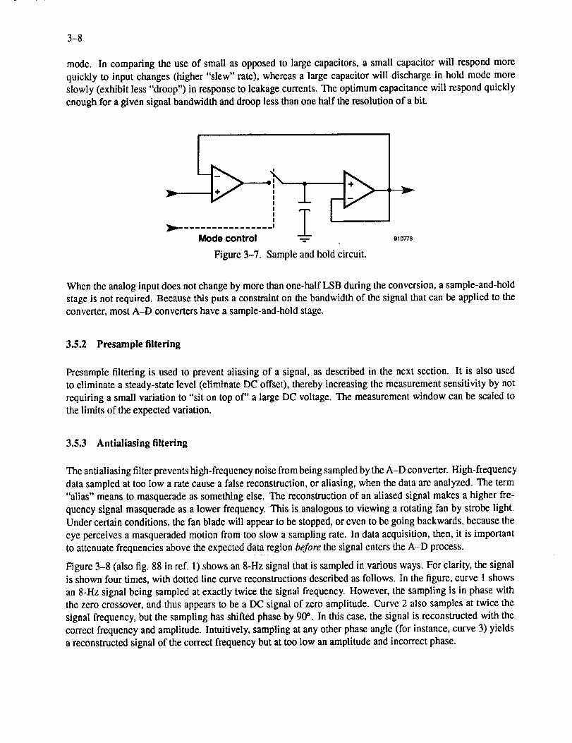
3-8
mode.In comparingtheuseof smallasopposedto large capacitors, a small capacitor will respond more
quickly to input changes (higher "slew" rate), whereas a large capacitor will discharge in hold mode more
slowly (exhibit less "droop") in response to leakage currents. The optimum capacitance will respond quickly
enough for a given signal bandwidth and droop less than one half the resolution of a bit.
Mode control -=- g10776
Figure 3-7. Sample and hold circuit.
When the analog input does not change by more than one-half LSB during the conversion, a sample-and-hold
stage is not required. Because this puts a constraint on the bandwidth of the signal that can be applied to the
convener, most A-D conveners have a sample-and-hold stage.
3.5.2 Presample filtering
Presample filtering is used to prevent aliasing of a signal, as described in the next section. It is also used
to eliminate a steady-state level (eliminate DC offset), thereby increasing the measurement sensitivity by not
requiring a small variation to "sit on top of" a large DC voltage. The measurement window can be scaled to
the limits of the expected variation.
3.5.3 Antialiasing filtering
The antialiasing filter prevents high-frequency noise from being sampled by the A-D converter. High-frequency
data sampled at too low a rate cause a false reconstruction, or aliasing, when the data are analyzed. The term
"alias" means to masquerade as something else. The reconstruction of an aliased signal makes a higher fre-
quency signal masquerade as a lower frequency. This is analogous to viewing a rotating fan by strobe light.
Under certain conditions, the fan blade will appear to be stopped, or even to be going backwards, because the
eye perceives a masqueraded motion from too slow a sampling rate. In data acquisition, then, it is important
to attenuate frequencies above the expected data region before the signal enters the A-D process.
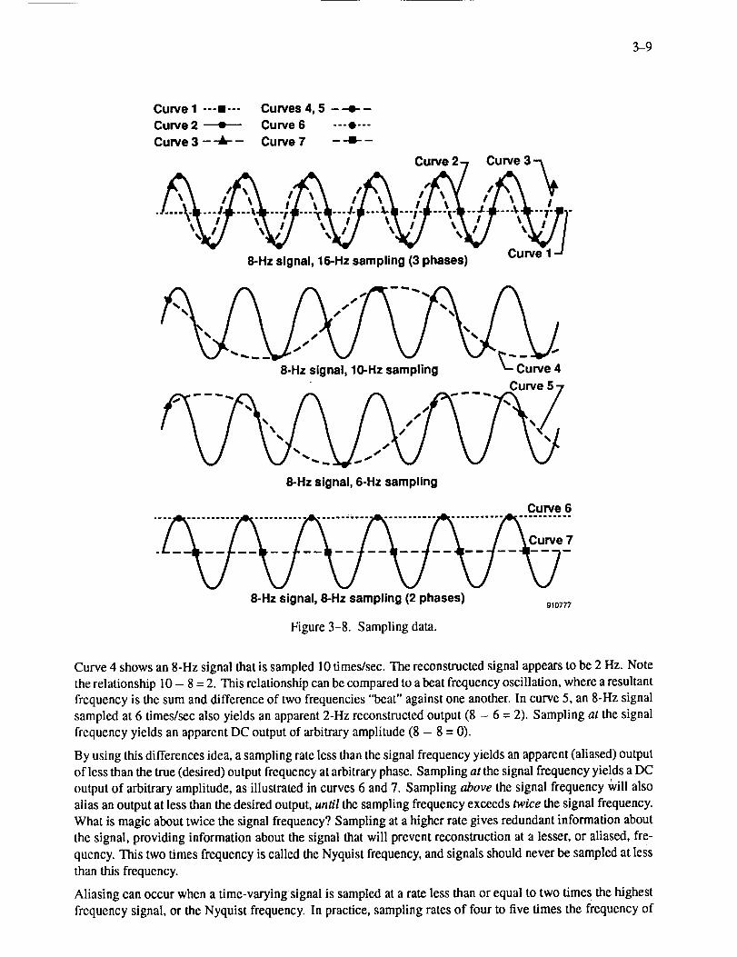
Figure 3-8 (also fig. 88 in ref. 1) shows an 8-Hz signal that is sampled in various ways. For clarity, the signal
is shown four times, with dotted line curve reconstructions described as follows. In the figure, curve 1 shows
an 8-Hz signal being sampled at exactly twice the signal frequency. However, the sampling is in phase with
the zero crossover, and thus appears to be a DC signal of zero amplitude. Curve 2 also samples at twice the
signal frequency, but the sampling has shifted phase by 90 ° . In this case, the signal is reconstructed with the
correct frequency and amplitude. Intuitively, sampling at any other phase angle (for instance, curve 3) yields
a reconstructed signal of the correct frequency but at too low an amplitude and incorrect phase.
3-9
Curve I ---a--- Curves 4, 5 ---e--Curve 2 ---e-- Curve 6 ---e---
Curve 3 - -_- - Curve 7 - -B- -
Curve 2- 7 Curve 3-_
I I I i _ I _IkI I I I I
• ,--;; -) --;;- --;,- -;t -;,--8-Hz signal, 16-Hz sampling (3 phases)
A A A.,--G--"A
Curve 5 -7
/
V.._V....vv8-Hz signal, 6-Hz sampling
Curve 6....... ==..= ........ =.. ....... ..=i... o-w!--- ....... ---=---- "'' ..... "''
. 7
8-Hz signal, 8-Hz sampling (2 phases) glo7_
Figure 3-8. Sampling data.
Curve 4 shows an 8-Hz signal that is sampled 10 times/sec. The reconstructed signal appears to be 2 Hz. Note
the relationship 10 - 8 = 2. This relationship can be compared to a beat frequency oscillation, where a resultant
frequency is the sum and difference of two frequencies "beat" against one another. In curve 5, an 8-Hz signal
sampled at 6 times/sec also yields an apparent 2-Hz reconstructed output (8 - 6 = 2). Sampling at the signal
frequency yields an apparent DC output of arbitrary amplitude (8 - 8 = 0).
By using this differences idea, a sampling rate less than the signal frequency yields an apparent (aliased) output
of less than the true (desired) output frequency at arbitrary phase. Sampling at the signal frequency yields a DC
output of arbitrary amplitude, as illustrated in curves 6 and 7. Sampling above the signal frequency _vill also
alias an output at less than the desired output, until the sampling frequency exceeds twice the signal frequency.
What is magic about twice the signal frequency? Sampling at a higher rate gives redundant information about
the signal, providing information about the signal that will prevent reconstruction at a lesser, or aliased, fre-
quency. This two times frequency is called the Nyquist frequency, and signals should never be sampled at less
than this frequency.
Aliasing can occur when a time-varying signal is sampled at a rate less than or equal to two times the highest
frequency signal, or the Nyquist frequency. In practice, sampling rates of four to five times the frequency of
3-10
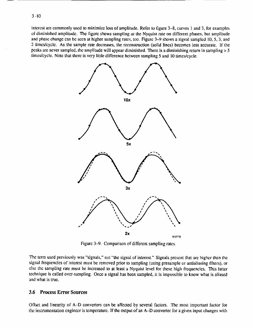
interestarecommonlyusedtominimizelossof amplitude.Referto figure3-8,curves1and3,for examplesof diminishedamplitude.Thefigureshowssamplingat the Nyquist rate on different phases, but amplitude
and phase change can be seen at higher sampling rates, too. Figure 3-9 shows a signal sampled 10, 5, 3, and
2 times/cycle. As the sample rate decreases, the reconstruction (solid lines) becomes less accurate. If the
peaks are never sampled, the amplitude will appear diminished. There is a diminishing return in sampling > 5
times/cycle. Note that there is very little difference between sampling 5 and 10 times/cycle.
lOx
5x
3x
I ! S_ I I •
2x910778
Figure 3-9. Comparison of different sampling rates.
The term used previously was "signals," not "the signal of interest." Signals present that are higher than the
signal frequencies of interest must be removed prior to sampling (using presample or antialiasing filters), or
else the sampling rate must be increased to at least a Nyquist level for these high frequencies. This latter
technique is called over-sampling. Once a signal has been sampled, it is impossible to know what is aliasedand what is true.
3.6 Process Error Sources
Offset and linearity of A-D converters can be affected by several factors. The most important factor for
the instrumentation engineer is temperature. If the output of an A-D converter for a given input changes with
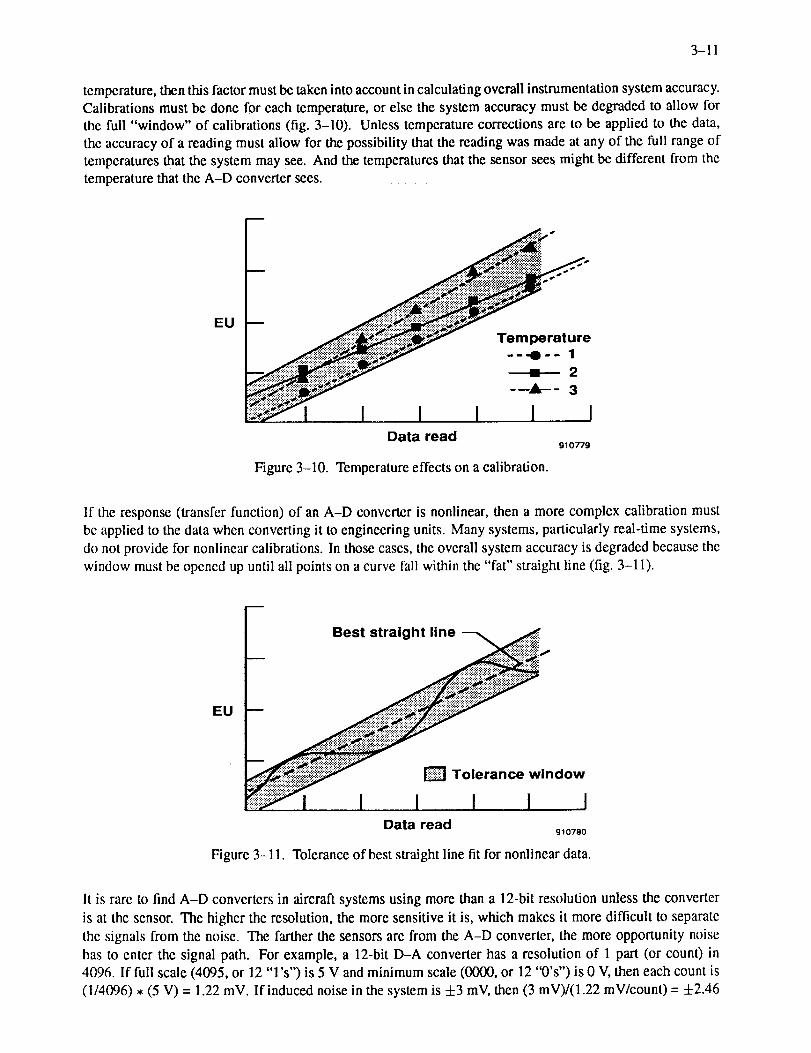
3-11
temperature,thenthisfactormustbetakenintoaccountincalculatingoverall instrumentation system accuracy.Calibrations must be done for each temperature, or else the system accuracy must be degraded to allow for
the full "window" of calibrations (fig. 3-10). Unless temperature corrections are to be applied to the data,
the accuracy of a reading must allow for the possibility that the reading was made at any of the full range of
temperatures that the system may see. And the temperatures that the sensor sees might be different from the
temperature that the A-D converter sees.
F _ _o"'::::i_:'i_'!"" "_i
___ __"'=================================="_:_ ., --
• ::::::::::::::::::::::: 3:: 'P• _;:;_;:;:;'_..:::_z-_.:," " "" "
---O--1
---_-'- 3
Data read910779
Figure 3-10. Temperature effects on a calibration.
If the response (transfer function) of an A-D converter is nonlinear, then a more complex calibration must
be applied to the data when converting it to engineering units. Many systems, particularly real-time systems,
do not provide for nonlinear calibrations. In those cases, the overall system accuracy is degraded because the
window must be opened up until all points on a curve fall within the "fat" straight line (fig. 3-11).
m
Best straight line _..::_:_ii_i_!!_.::il
EU
indow
I I_ I I I I
Data read910780
Figure 3-11. Tolerance of best straight line fit for nonlinear data.
It is rare to find A-D converters in aircraft systems using more than a 12-bit resolution unless the converter
is at the sensor. The higher the resolution, the more sensitive it is, which makes it more difficult to separate
the signals from the noise. The farther the sensors are from the A-D converter, the more opportunity noise
has to enter the signal path. For example, a 12-bit D-A converter has a resolution of 1 part (or count) in
4096. If full scale (4095, or 12 "1 's") is 5 V and minimum scale (0000, or 12 "O's") is 0 V, then each count is
(1/4096) • (5 V) = 1.22 mV. If induced noise in the system is 4-3 mV, then (3 mV)/(1.22 mV/count) = 4-2.46
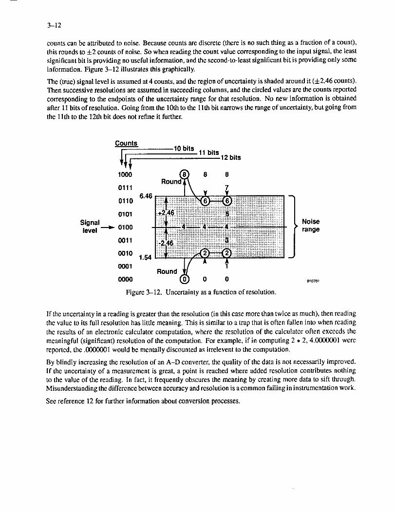
3-12
counts can be attributed to noise. Because counts are discrete (there is no such thing as a fraction of a count),
this rounds to +2 counts of noise. So when reading the count value corresponding to the input signal, the least
significant bit is providing no useful information, and the second-to-least significant bit is providing only some
information. Figure 3-12 illustrates this graphically.
The (true) signal level is assumed at 4 counts, and the region of uncertainty is shaded around it (+2.46 counts).
Then successive resolutions are assumed in succeeding columns, and the circled values are the counts reported
corresponding to the endpoints of the uncertainty range for that resolution. No new information is obtained
after 11 bits of resolution. Going from the 10th to the 11th bit narrows the range of uncertainty, but going from
the llth to the 12th bit does not refine it further.
Signallevel
Counts10 bits
-,_Jf_ 11 bits 12 bits
Roun0111
i!i i il;i:iiiil;:i iiiilloo,o,.,411}i ! :ii)iiiiii
0001 Round (_ A 1A0000 0 0
Figure 3-12. Uncertainty as a function of resolution.
I Noise
range
I
J
910781
If the uncertainty in a reading is greater than the resolution (in this case more than twice as much), then reading
the value to its full resolution has little meaning. This is similar to a trap that is often fallen into when reading
the results of an electronic calculator computation, where the resolution of the calculator often exceeds the
meaningful (significant) resolution of the computation. For example, if in computing 2 • 2, 4.0000001 were
reported, the .0000001 would be mentally discounted as irrelevent to the computation.
By blindly increasing the resolution of an A-D converter, the quality of the data is not necessarily improved.
If the uncertainty of a measurement is great, a point is reached where added resolution contributes nothing
to the value of the reading. In fact, it frequently obscures the meaning by creating more data to sift through.
Misunderstanding the difference between accuracy and resolution is a common failing in instrumentation work.
See reference 12 for further information about conversion processes.
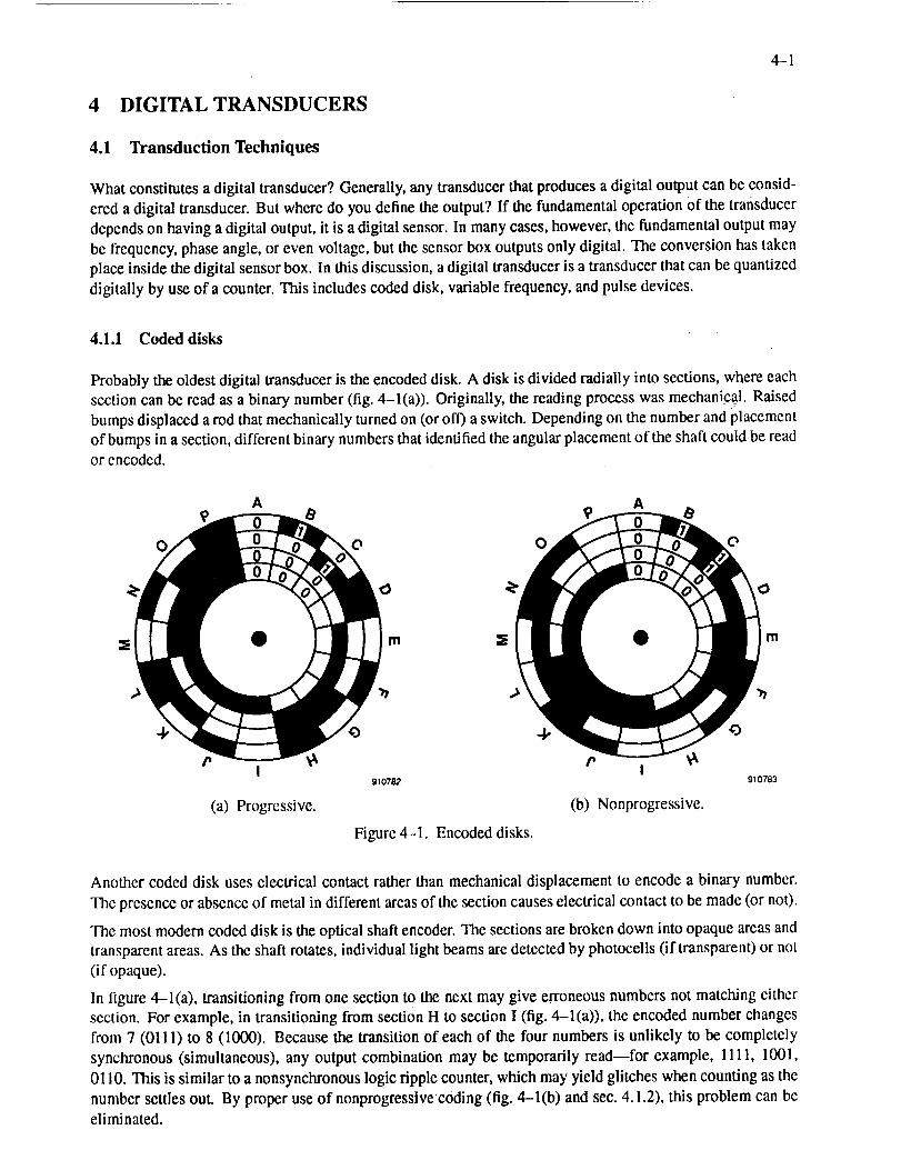
4-1
4 DIGITAL TRANSDUCERS
4.1 Transduction Techniques
What constitutes a digital transducer? Generally, any transducer that produces a digital output can be consid-
ered a digital transducer. But where do you define the output? If the fundamental operation of the transducer
depends on having a digital output, it is a digital sensor. In many cases, however, the fundamental output may
be frequency, phase angle, or even voltage, but the sensor box outputs only digital. The conversion has taken
place inside the digital sensor box. In this discussion, a digital transducer is a transducer that can be quantized
digitally by use of a counter. This includes coded disk, variable frequency, and pulse devices.
4.1.1 Coded disks
Probably the oldest digital transducer is the encoded disk. A disk is divided radially into sections, where each
section can be read as a binary number (fig. 4-1(a)). Originally, the reading process was mechanical. Raised
bumps displaced a rod that mechanically turned on (or off) a switch. Depending on the number and placement
of bumps in a section, different binary numbers that identified the angular placement of the shaft could be read
or encoded.
A A
0 0 0
m m
4 O 4
r _b r _bI I
910782
(a) Progressive. (b) Nonprogressive.
Figure 4-1. Encoded disks.
910783
Another coded disk uses electrical contact rather than mechanical displacement to encode a binary number.
The presence or absence of metal in different areas of the section causes electrical contact to be made (or not).
The most modem coded disk is the optical shaft encoder. The sections are broken down into opaque areas and
transparent areas. As the shaft rotates, individual light beams are detected by photocells (if transparent) or not
(if opaque).
In figure 4--l(a), transitioning from one section to the next may give erroneous numbers not matching either
section. For example, in transitioning from section H to section I (fig. 4-1(a)), the encoded number changes
from 7 (0111) to 8 (1000). Because the transition of each of the four numbers is unlikely to be completely
synchronous (simultaneous), any output combination may be temporarily read--for example, 1111, 1001,
0110. This is similar to a nonsynchronous logic ripple counter, which may yield glitches when counting as the
number settles out. By proper use of nonprogressive coding (fig. 4-1(b) and sec. 4.1.2), this problem can be
eliminated.
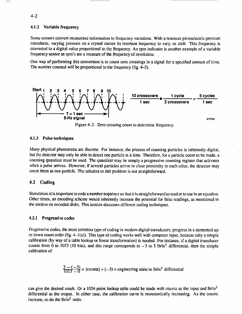
4-2
4.1.2 Variable frequency
Some sensors convert measurand information to frequency variations. With a resonant piezoelectric pressure
transducer, varying pressure on a crystal causes its resonant frequency to vary, or shift. This frequency is
converted to a digital value proportional to the frequency. An rpm indicator is another example of a variable
frequency sensor as rpm's are a measure of the frequency of revolution.
One way of performing this conversion is to count zero crossings in a signal for a specified amount of time.
The number counted will be proportional to the frequency (fig. 4-2).
Start1 2 3 4 5 6 7 8 9 10
I..x, ,..., ,.._, ,¢x, ,¢x, I,.x, , 10 crossovers •
5-Hz signal
Figure 4-2. Zero-crossing count to determine frequency.
1 cycle 5 cycles
gt0784
2 crossovers 1 sec
4.1.3 Pulse techniques
Many physical phenomena are discrete. For instance, the process of counting particles is inherently digital,
but the detector may only be able to detect one particle at a time, Therefore, for a particle count to be made, a
counting quantizer must be used. The quantizer may be simply a progressive counting register that activates
when a pulse arrives. However, if several particles arrive in close proximity to each other, the detector may
count them as one particle. The solution to this problem is not straightforward.
4.2 Coding
Sometimes it is important to code a number sequence so that it is straightforward to read or to use in an equation.
Other times, an encoding scheme would inherently increase the potential for false readings, as mentioned in
the section on encoded disks. This section discusses different coding techniques.
4.2.1 Progressive codes
Progressive codes, the most common type of coding in modern digital transducers, progress in a numerical up
or down count order (fig. 4-1(a)). This type of coding works well with computer input, because only a simple
calibration (by way of a table lookup or linear transformation) is needed. For instance, if a digital transducer
counts from 0 to 1023 (10 bits), and this range corresponds to -3 to 3 lb/in 2 differential, then the simplecalibration of
]0-_3( -3_ × (counts)+ (-3)= engineering units in Ib/in 2 differential
can give the desired result. Or a 1024-point lookup table could be made with counts as the input and lb/in 2
differential as the output. In either case, the calibration curve is monotonically increasing. As the counts
increase, so do the Ib/in 2 units.
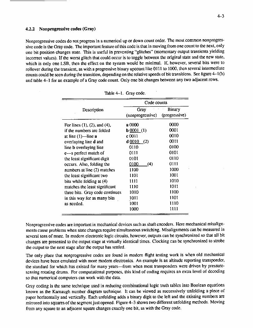
4-3
4.2.2 Nonprogressive codes (Gray)
Nonprogressive codes do not progress in a numerical up or down count order. The most common nonprogres-
sive code is the Gray code. The important feature of this code is that in moving from one count to the next, only
one bit position changes state. This is useful in preventing "glitches" (momentary output transients yielding
incorrect values). If the worst glitch that could occur is to toggle between the original state and the new state,
which is only one LSB, then the effect on the system would be minimal. If, however, several bits were to
rollover during the transient, as with a progressive binary upcount like 0111 to 1000, then several intermediate
counts could be seen during the transition, depending on the relative speeds of bit transitions. See figure 4--l(b)
and table 4-1 for an example of a Gray code count. Only one bit changes between any two adjacent rows.
Table 4-1. Gray code.
Description
Code counts
Gray Binary
(nonprogressive) (progressive)
For lines (1), (2), and (4), a 0000
if the numbers are folded b 0001 .(1)
at line (l)--line a c 0011
overlaying line d and d 0010 .(2)
0000
0001
0010
0011
line b overlaying line 0110 0100
c--a perfect match of 0111 0101
the least significant digit 0101 0110
occurs. Also, folding the 0100 (4) 0111
numbers at line (2) matches 1100 1000
the least significant two 1101 1001
bits while folding at (4) 1111 1010
matches the least significant 1110 1011
three bits. Gray code continues 1010 1100
in this way for as many bits 1011 1101as needed. 1001 1110
1000 1111
Nonprogressive codes are important in mechanical devices such as shaft encoders. Here mechanical misalign-
ments cause problems when state changes require simultaneous switching. Misalignments can be measured in
several tens of msec. In modern electronic logic circuits, however, outputs can be synchronized so that all bit
changes are presented to the output stage at virtually identical times. Clocking can be synchronized to strobe
the output to the next stage after the output has settled.
The only place that nonprogressive codes are found in modern flight testing work is when old mechanical
devices have been emulated with more modern electronics. An example is an altitude reporting transponder,
the standard for which has existed for many years--from when most transponders were driven by pressure-
sensing rotating drums. For computational purposes, this kind of coding requires an extra level of decoding
so that numerical computers can work with the data.
Gray coding is the same technique used in reducing combinational logic truth tables into Boolean equations
known as the Karnaugh number diagram technique. It can be viewed as successively unfolding a piece of
paper horizontally and vertically. Each unfolding adds a binary digit to the left and the existing numbers are
mirrored into squares of the segment just opened. Figure 4-3 shows two different unfolding methods. Moving
from any square to an adjacent square changes exactly one bit, as with the Gray code.
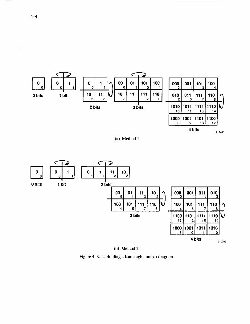
4-4
Fq0 bits
_T_IOol,I. o ,1 0 1 . _ 0
1 bil 10 11 _ 102 3 2
2 bits
c"_01 101 100
1 5 4
11 111 1103 7 6
3 bits
(a) Method 1.
000 001 101 1000 I 1 5 4
1010 1011 1111 111010 11 15 14
1000 1001 1101 11008 9 13 12
4 bits910785
D0 bits 1 bit
iool',_"31,o21I
2 bits
O0 01 11 100 1 3 2
100 101 111 1104 5 7 6
3 bits
(b) Method 2.
Figure 4-3. Unfolding a Karnaugh number diagram.
000 001 011 0100 1 3 2
100 101 111 1104 5 7 6
1100 1101 1111 111012 13 15J 14
1000 1001 1011 10108 9 11 10
4 bits910786
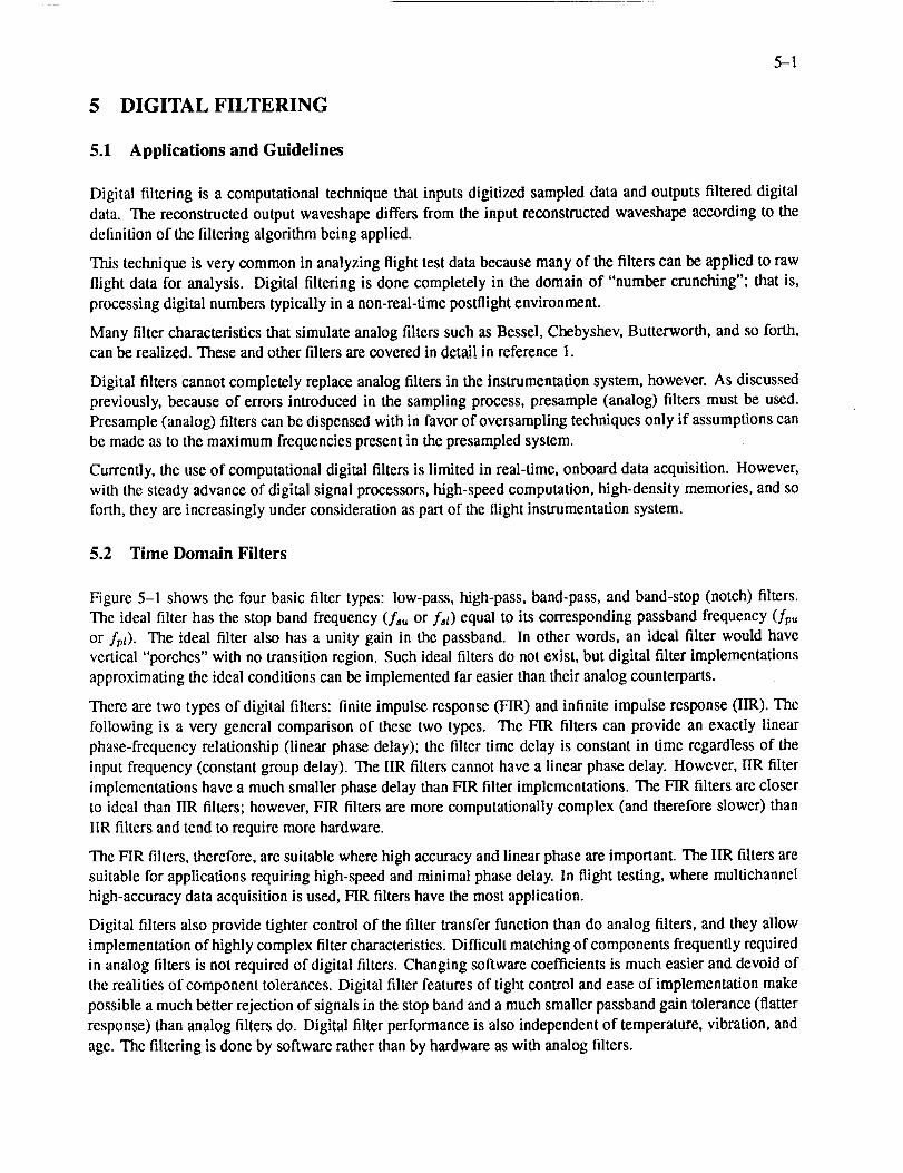
5-1
5 DIGITAL FILTERING
5.1 Applications and Guidelines
Digital filtering is a computational technique that inputs digitized sampled data and outputs filtered digital
data. The reconstructed output waveshape differs from the input reconstructed waveshape according to the
definition of the filtering algorithm being applied.
This technique is very common in analyzing flight test data because many of the filters can be applied to raw
flight data for analysis. Digital filtering is done completely in the domain of "number crunching"; that is,
processing digital numbers typically in a non-real-time postflight environment.
Many filter characteristics that simulate analog filters such as Bessel, Chebyshev, Butterworth, and so forth,can be realized. These and other filters are covered in detail in reference 1.
Digital filters cannot completely replace analog filters in the instrumentation system, however. As discussed
previously, because of errors introduced in the sampling process, presample (analog) filters must be used.
Presample (analog) filters can be dispensed with in favor of oversampling techniques only if assumptions can
be made as to the maximum frequencies present in the presampled system.
Currently, the use of computational digital filters is limited in real-time, onboard data acquisition. However,
with the steady advance of digital signal processors, high-speed computation, high-density memories, and so
forth, they are increasingly under consideration as part of the flight instrumentation system.
5.2 Time Domain Filters
Figure 5-1 shows the four basic filter types: low-pass, high-pass, band-pass, and band-stop (notch) filters.
The ideal filter has the stop band frequency (f_,, or f_l) equal to its corresponding passband frequency (fr,_,
or fpl). The ideal filter also has a unity gain in the passband. In other words, an ideal filter would havevertical "porches" with no transition region. Such ideal filters do not exist, but digital filter implementations
approximating the ideal conditions can be implemented far easier than their analog counterparts.
There are two types of digital filters: finite impulse response (FIR) and infinite impulse response (IIR). The
following is a very general comparison of these two types. The FIR filters can provide an exactly linear
phase-frequency relationship (linear phase delay); the filter time delay is constant in time regardless of the
input frequency (constant group delay). The IIR filters cannot have a linear phase delay. However, IIR filter
implementations have a much smaller phase delay than FIR filter implementations. The FIR filters are closer
to ideal than IIR filters; however, FIR filters are more computationany complex (and therefore slower) than
IIR filters and tend to require more hardware.
The FIR filters, therefore, are suitable where high accuracy and linear phase are important. The IIR filters are
suitable for applications requiring high-speed and minimal phase delay. In flight testing, where multichannel
high-accuracy data acquisition is used, FIR filters have the most application.
Digital filters also provide tighter control of the filter transfer function than do analog filters, and they allow
implementation of highly complex filter characteristics. Difficult matching of components frequently required
in analog filters is not required of digital filters. Changing software coefficients is much easier and devoid of
the realities of component tolerances. Digital filter features of tight control and ease of implementation make
possible a much better rejection of signals in the stop band and a much smaller passband gain tolerance (flatter
response) than analog filters do. Digital filter performance is also independent of temperature, vibration, and
age. The filtering is done by software rather than by hardware as with analog filters.
5-2
Magnitude
Lowpass
1
!fpu fsu
Bandpass
!
i Ifsl fpl
i I
I
% fsu
Magnitude
Highpass
lifsl fpl
Frequency, Hz
Figure 5-1. "time domain filters.
Bandstop
: i
i i ''I ifpl fsl fsu%
Frequency, Hz910787
5.2.1 Nonrecursive filters
Digital filters arc nonrecursive if the current output sample is a function of the present and of a few past
inputs. Another name for nonrccursive filtcrs is finite impulse response. This type of filter has no equivalent
in analog circuitry.
5.2.2 Recursive filters
Digital filters are recursive if the current output sample is a function of present and all past input samples.
Rccursive filters are also known as infinite impulse response. This type of filter is realizable in analog circuitry.
See references 13 and 14 for an indepth mathematical discussion of digital filters.
5.2.3 Switched capacitor filters
A common analog filter in use is the resistance-capacitance (Re) filter. This filter's characteristics can be al-
tered by changing either the resistance or the capacitance of the filter elements. This is accomplished either
by removing the filter signal conditioning card from the system and manually replacing the elements, or by
remotely switching components by switches, relays, or analog multiplexers. Manual removal is time consum-
ing and disturbs the system. Remote switching typically requires bulky components and therefore lowers the
density of circuitry required.
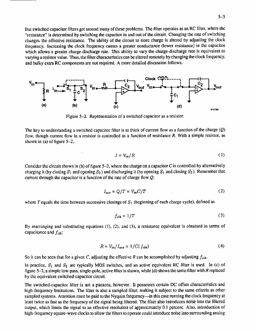
5-3
Butswitchedcapacitorfiltersgetaroundmanyof these problems. The filter operates as an RC filter, where the
"resistance" is determined by switching the capacitor in and out of the circuit. Changing the rate of switching
changes the effective resistance. The ability of the circuit to store charge is altered by adjusting the clock
frequency. Increasing the clock frequency causes a greater conductance 0ower resistance) in the capacitor
which allows a greater charge-discharge rate. This ability to vary the charge-discharge rate is equivalent to
varying a resistor value. Thus, the filter characteristics can be altered remotely by changing the clock frequency,
and bulky extra RC components are not required. A more detailed discussion follows.
(a) (b)
_ Clock _ ..... _ r"--I ('--'1Vin VIne----o__L _, _, _Vo ut
(c) (d)910788
Figure 5-2. Representation of a switched capacitor as a resistor.
The key to understanding a switched capacitor filter is to think of current flow as a function of the charge (Q)
flow, though current flow in a resistor is controlled as a function of resistance R. With a simple resistor, as
shown in (a) of figure 5-2,
I = (1)
Consider the circuit shown in (b) of figure 5-2, where the charge on a capacitor C is controlled by alternatively
charging it (by closing S1 and opening $2 ) and discharging it (by opening Sl and closing $2). Remember that
current through the capacitor is a function of the rate of charge flow Q:
io, = Q/7" = (2)
where T equals the time between successive closings of Sl (beginning of each charge cycle), defined as
folk = l/T (3)
By rearranging and substituting equations (1), (2), and (3), a resistance equivalent is obtained in terms of
capacitance and fdk:
R = Vin/Iave = 1/C(fdk) (4)
So it can be seen that for a given C, adjusting the effective R can be accomplished by adjusting fak.
In practice, Sl and 5'2 are typically MOS switches, and an active equivalent RC filter is used. In (c) of
figure 5-2, a simple low-pass, single-pole, active filter is shown, while (d) shows the same filter with R replaced
by the equivalent switched-capacitor circuit.
The switched-capacitor filter is not a panacea, however. It possesses certain DC offset characteristics and
high-frequency limitations. The filter is also a sampled filter, making it subject to the same criteria as other
sampled systems. Attention must be paid to the Nyquist frequency--in this case running the clock frequency at
least twice as fast as the frequency of the signal being filtered. The filter also introduces noise into the filtered
output, which limits the signal to an effective resolution of approximately 0.1 percent. Also, introduction of
high-frequency square-wave clocks to allow the filters to operate could introduce noise into surrounding analog
5-4
lines.Butimproveddesignsandtheirabilitytobepackagedinmonolithicpartsalongwithother elements of
signal conditioning makes them of increasing value.
See reference 15 for a discussion of switched-capacitor filters.
5.3 Statistical Filtering
Statistical filtering is the interpretation of data in a distribution sense. For instance, creating a histogram
where each column represents the pressure at a particular spacial position or the number of a particular sized
particle detected.
There is much interest in measuring aircraft vibration, particularly in clearing an aircraft structurally for dif-
ferent flight envelopes. These vibrations are high in frequency. Typically, the frequencies are modulated on
an FM (frequency modulation) carder and transmitted to tape or ground facilities. If a sampled system is used
to measure the frequency, samples would need to be taken at least at twice the frequency (Nyquist theorem) of
the measured system. As discussed in section 3.5.3, however, the system should be sampled at greater than this
frequency if proper phase and amplitude is to be maintained. In either case, for safety of flight monitoring, this
data must be telemetered and analyzed to determine frequency content. The process requires a wide bandwidth
for transmission and a computationally intensive activity at the receiving end. If an appropriate statistical filter
is applied at the point of sampling, the data may be reduced to reporting just the frequency modes (frequencies
and amplitudes) with a considerably reduced transmission bandwidth requirement.
5.4 Data Compression Filtering
The process of compressing data is an act of filtering. The simplest form of data compression filtering is
to examine a data parameter and not pass it on if it has not changed from the last time it was sent. This
form does not reduce the overall information content. The data can be reconstructed easily with some extra
computational capability. The only drawback to this technique is in cases where data are lost as a result of
transmission dropout or interference. If the data chose that moment to update their value, and that information
is not updated again, then significant errors can creep into the data being analyzed. In short, missing one value
that is seldom sent is more significant than missing one value that is frequently sent. For example, an aircraft
is not likely to swing its landing gear very often (hopefully, an even number of times)--certainly less often
than the aircraft speed changes occur. Sending the gear position updates at the same rate as the speed updates
is a waste of bandwidth resources.
Variations on this form of filtering include creating a window to define what constitutes a "change." For
instance, the algorithm might say, "send a new temperature value if it has changed by more than 0.2°F since
the last time the value was sent." In this case, some information content will probably be lost, as with most
"normal" filter implementation s. But what constitutes a significant change can be defined.
5.5 Pitfalls (Problem Areas) of Digital Filtering
Digital filtering requires much computation. Until recently, computations could only be done in non-real-time
(during postflight data reduction). Inclusion of modern digital signal processors (DSP's) on aircraft data acqui-
sition systems requires skills not normally possessed by experienced instrumentation engineers. Fortunately,
manufacturers are hiding the mathematical magic and are requiring implementers to input the same design
criteria as they did for analog filters (passband frequency, stop band frequency, stop band noise rejection, pass-
band gain tolerance, and sampling frequency). The only addition is deciding the number of coefficients to use,
and even this number may be set to a recommended value determined by the rest of the criteria. However,
signal processors exist that require the engineer to write the digital filter design code.
It must be reiterated that unless the measurand is oversampled sufficiently (remembering that sufficiency must
be determinable), it must be antialias filtered prior to sampling or entry into a digital filter.
6-1
6 DIGITAL COMMUNICATION
6.1 Technology Choices
There are three basic methods for transferring digital data: copper wire, telemetry, and optical fiber.
method has its advantages and disadvantages.
Each
6.1.1 Copper wire
This method is the simplest and oldest medium of transfer for digital data. Interfacing to transmission and
receiving equipment is simple and straightforward. However, it does have shortcomings. Digital transmission
is usually a series of square waves. Square waves can be considered as a collection of an infinite number of
sine waves at different frequencies and amplitudes. Cables selectively attenuate higher frequencies. Because
the higher frequencies contribute the most to the "sharpness" of a square wave's rise and fall time, the pulses
will round off and spread (disperse). At long cable lengths, the round off becomes significant. At high pulse
rates, the rounding can cause difficulty in distinguishing closely spaced pulses.
In addition, copper-wired transmission is susceptible to interference from electric and magnetic fields. Twisting
wires can minimize magnetic field interference, and shielding the wires can minimize electric field interference.
"Crosstalk," or the picking up of signals from adjacent channels, is a frequent result of these fields.
Another problem in copper-wired transmissions can arise if the signal return is "ground" referenced at each
end. This is a so-caned "single-ended" or "unbalanced" connection. The problem here is that each end of the
"ground" is at a different voltage potential because of stray ground currents flowing in the nonzero resistance
of the conduction path between the two ground terminations. There are many sources of electric energy in an
aircraft. The more sources that are ground referenced to the same conductive medium (typically the skin or
frame of a metal aircraft), the more currents are induced. Therefore, there is more voltage difference between
any two points, which can significantly cut into the noise margin.
Finally, at longer cable lengths and higher pulse rates, transmission line effects are seen. Discontinuities, or
mismatches, in impedances will cause reflections that can significantly distort the pulses.
6.1.2 Fiber optics
Fiber optic data transmission is the most important technical development in data communication in recent
years. With it, almost all of the disadvantages of copper-wired transmission disappear. Fiber optics allows
for extremely high data rates over long distances and is virtually immune to electrical interference, grounding
problems, and static. It is also extremely lightweight.
These are important considerations in aircraft--especially weight and noise immunity. Fiber optics has a few
disadvantages, however. Currently, fiber optic transmission requires a change in energy from electrical to
optical and back. This change requires additional hardware. More importantly, the optical fiber connections
at this stage of development are difficult and require a special skill for use.
Connection techniques have become easier, however. The use of laser diodes lessens connection losses so
connection alignments are not as critical.
Instrumenting an aircraft for flight test frequently requires modifications and additions to existing aircraft
wiring. A flight test program usually requires modification of the wiring for different phases of testing. Because
connections are the single most difficult part of a fiber optic installation, this situation presents difficulties. Fiber
connections work best if there are no connections. Common practices of bulkhead disconnects in wiring can
significantly degrade an optical signal. A single optical fiber should extend from one end to the other because
splitting off signals for bus-type connections is tricky.
6-2
Todaythereis little use of optical fibers in "wiring" instrumentation for flight test. Some organizations have
experimented with it, abandoning it until the technology of interconnecting systems improves.
Optical fibers are, however, finding use in digital flight control systems, particularly in military aircraft. These
installations don't require most of the dynamic reconfiguring that flight test instrumentation does. The advan-
tages of lighter weight, electromagnetic interference (EMI) immunity, and high data rates win out. However,
because these systems must be monitored for flight testing, instrumentation crews are being forced to work
with optical fibers.
6.1.3 Telemetry
Telemetry is the broadcasting of digital information by way of radio frequency energy. Its use in flight testing
is extremely important. Telemetry provides ground-based evaluators with instrumentation data in real time
so that safety of flight parameters can be monitored. It also provides a record of the test flight if the onboard
recording device is damaged or destroyed in a crash. In an aircraft without an onboard recorder, telemetry can
provide the only record of flight data.
6.2 Transmission Timing Choices
6.2.1 Synchronous
Synchronous transmission of data transmits in a regular, predictable, continuous stream. The Inter-Range
Instrumentation Group (IRIG) pulse-code modulation (PCM) signals are sent in this manner. The receiving
equipment locks onto PCM synchronization word patterns that are unique and not found in the rest of the data
stream. Thus, the equipment can keep track of its position in the PCM stream. There are two advantages
to this technique. First, with the appropriate PCM sampling system, data are sampled at regular, predictable
intervals and work with linear reconstruction techniques using simple computer programs. Second, standard
IRIG decommutation equipment can be used to receive and interpret the data.
The disadvantage of this method of data transmission is that for data changing value much slower than the
sampling rate, bandwidth is wasted. Synchronous transmission requires regular sampling of data as each data
parameter is identifiable by its own unique timeslot. Even if a parameter has the same value as the last time
it was sampled, it must be transmitted regardless because that timeslot has been assigned to it. Obviously, if
much of the data are static, then much redundant data are transmitted.
6.2.2 Asynchronous
In asynchronous transmission, data are transmitted only when there is new information. The signal medium
(RF, data lines, and so on) is "dead" between transmissions. During times of high message traffic, the stream
may appear to be continuous, but some minimum dead, or "stop" time is proscribed between message words
or groups of words. This technique is useful when unnecessary use of bandwidth is to be minimized.
These are two disadvantages to asynchronous transmission. First, each data message must carry label and
sample time information to fully identify a parameter or group of parameters. This, as well as the requirement
for a certain stop time, increases the amount of time to send data, a drawback if much data require transmission.
Second, receiving equipment is complicated because more intelligence is needed to decode the data. Each data
word or packet must have its label(s) examined to determine what data it is.
Sometimes hybrid approaches are used. With the F-15 digital electronic engine control (DEEC) system tested
at the NASA Ames Research Center's Dryden Flight Research Facility, data were sent as asynchronous 8-bit
bytes (with 1 start bit and 2 stop bits). However, the contents, when constructed, resembled a synchronous
6-3
data stream complete with frame synchronizers. This is perhaps the simplest approach in terms of hardware
and software required for data sent over wire at moderately slow data rates.
In another case, asynchronous data from a military standard (MIL-STD-1553) data bus (discussed in
sec. 6.5.1) was reformatted into a synchronous, frame-synchronized data stream that made use of dummy
data words when there was dead time (ref. 16).
6.2.3 Isochronous
Isochronous transmission is data transmitted based on a direct relationship to events being monitored. For
example, in helicopter testing, it is more significant to time data relative to the revolution rate of the rotor
blade than it is to an arbitrary (and therefore, nonsynchronized) time.
6.3 Communication Format Choices
6.3.1 Serial transfer
Serial transfer is sending digital data one bit at a time. It takes several "bit times" (8, 10, 16, 32, and so on) for
a unit of digital information (a word) to be transferred. This form of transfer requires the fewest connections
between a transmitting and receiving system, usually only two electrical wires or one optical fiber. Serial
transfer saves weight and, in the case of telemetry transmission of data, saves RF spectrum bandwidth. With
today's LSI components, it is no more complex than sending data in a parallel (see sec. 6.3.2).
Serial data can be regarded in one of three ways: unidirectional, half duplex, or full duplex.
Unidirectional transmission, as the name implies, is data sent in one direction only. The transmitting end
requires no information from the receiving end. It isjust"broadcasting" the data to whatever might be listening.
This is the mode used when sending telemetry from an aircraft to ground stations or to onboard recorders.
Half-duplex transmission sends data both ways, but only one direction at a time. The best example of this is
a two-way radio, where each station can transmit over the same frequency by taking turns. Various standard
practices are developed to know whose turn it is to transmit. The same is true of half-duplex data transmission.
This form was very common in the early days of radio teletype, computer-teletype links, and, currently, shared
data bus connections like MIL-STD- 1553 (sec. 6.5.1).
Fun-duplex transmission sends data both ways at the same time. A telephone connection is a good example.
Both parties can converse simultaneously, although with most humans this would make little sense. However, it
does relax protocol requirements. A talker can be interrupted. In data communications, more than interruptions
can be made. Data can flow in both directions at the same time, and can keep each end informed of the other's
comprehension. (Is the receiver's buffer full? Has it detected an error?) Full-duplex connections make the
most sense in point-to-point connections between computer systems. Also, they are the most convenient form
in terminal-to-computer connections, and are the most common form in use. In its simplest form, another pair
of wires is added to allow information to flow back, as with ARINC 429 discussed in section 6.5.2.2. In a more
complex form, multiple frequencies and phases over the same pair of wires are used. Appropriate filtering at
each end separates each frequency into the appropriate interpretation of digital data. This is how telephone
full-dulSlex MODEM's function.
6.3.2 Parallel transfer
Parallel data transfer is the fastest way to transfer digital data. An entire digital entity, or word (for example,
8, 10, 16, 32 bits), is sent at one time. If several words are required to make up a message, then this type of
6--4
transfer is called word serial as only one word is sent at a time. Theoretically, a parallel transfer can be ntimes
faster than a bit serial transfer, where n is the number of bits in the word.
Parallel transfer is discussed only in relation to wired connections. A parallel transfer in telemetry would
require an extremely wide bandwidth, or range of frequencies, and an enormous amount of transmitting and
receiving equipment to effect a parallel signal path.
There is a lack of standards in parallel connections. Printer ports use a "Centronics" standard (unidirectional),
and many computer backplanes are using bus standards (VME, MULTIBUS, G-64, and so forth).
In summary, parallel connections offer the fastest, least protocol-complex data transfer while adding intercon-
nection complexity (more wires) and weight to the solution.
6.4 Data Formats
6.4.1 Timing and synchronization
The most common method of data formatting in flight test is PCM. Data are sampled and sent in a bit serial
fashion on a regular, predictable, timed cycle. To decode the information, synchronization words are sent to
mark the beginning of a group, or frame, of information.
The location of a word relative to the synchronization words determines the significance, or label, of that word
as opposed to each word having a label attached. This technique is simple to encode and makes efficient use of
bandwidth, wasting only those words required for synchronization. However, it is difficult to decode without
using commercial decoding equipment, and requires data to always be sent. The data are sent even if the
information has not changed from the last transmission, resulting in wasted bandwidth.
The PCM transmission following IRIG standards is a unidirectional transfer. If the receiving station detects
questionable data, it has the option of keeping it or ignoring it. It cannot direct the transmitter to retransmit it.
Because the detection of errors is in the form of recognizing the synchronization words at the proper time, if it
doesn't see what it expects, then it must assume that the entire last frame of information is suspect (see ref. 1).
6.4.2 Error detection and correction
6.4.2.1 Parity bit
The simplest form of error detection is the parity bit. The transmitting device computes a parity bit for each data
word sent and combines the bit with the data word to form a transmitted word. The receiving device receives
this word; performs its own computation of what the parity bit should be; compares it to the transmitted parity
bit; and, if different, shows that an error has occurred.
The calculation is a simple one. The word, being binary, consists of l's and O's. Count the number of 1's that
occur in the word (bit position is not importan0, and see if there are an odd or even number of l's. If the system
is designed to use "odd parity," then the total number of l's in the transmitted word (including the parity bit)
must be an odd number. The parity bit is then set to either 1 or 0 accordingly. An "even parity" system adjusts
the parity bit so that an even number of 1's are transmitted. Either way, this system will only detect an oddnumber of errors. An even number of errors will cancel each other out and the error will go undetected. Note
also that there is no way of determining where the error is in the word, only that an odd number has occurred.
Therefore, this is an error detection, but not an error correction, scheme.
6-5
6.4.2.2 Error correction code
Error correction codes (ECC's) are clever mathematical techniques for not only determining that errors have
occurred, but also for learning in which bits they have occurred. Because this is binary data, knowing that a
particular bit is in error infers that the opposite logic level is the correct data; thus the error can be corrected.
A simple, effective way of doing this is to retransmit a word several times and then compare them, throwing
out the words that don't match the majority. This, however, is extremely wasteful of bandwidth and isn't as
effective as ECC's. The ECC's typically add only 25 to 45 percent to the bandwidth, while providing better
checks than majority voting.
The ECC's are used extensively in deep space probes. Much of the information being sent is imaging, so
every bit is important. This is a prime example of where it would be impractical to request that the information
be retransmitted because of an error detection. The request time delay is too great because of the distances
involved. So instead of retransmission request on error, ECC is used. The ECC requires a bandwidth increase
(sending data faster), unless it is acceptable to decrease the overall update rate. This is a result of increased
overhead in the form of more bits (the ECC bits) requiring transmission.
In flight testing, ECC is less important. The rapid repeat rate of the data cycle makes it easier to accept an
occasional lost frame. However, these techniques will see increased usage in flight test as onboard processing in
data acquisition systems becomes more common. Therefore, it is good to be familiar with the basic mechanism.
An example of a popular ECC technique is the Hamming code. Data are encoded so that a decode matrix,
called a parity-check matrix, is used to extract it. If ra bits are actual information, then n is the total number
of bits that must be sent. Thus, m and n are related by the formula
where/¢ is the number of rows in the parity-check matrix, and
n= 2 k - 1
The best way to describe this code is by example. If k = 2, then the parity-check matrix H is a k row, n
column (k x n, or 2 x 3 in this case) matrix with m = 1, n = 3. So 3 - 1 = 2 extra bits sent for each actual
information bit. This is termed a single-error-correcting rate of R = m/n = 1/3, or 1 out of every 3 bits sentis information.
Also, if k = 3, then H is a 3 × 7 matrix and m = 4, n = 7. So 7 - 4 = 3 extra bits sent for every 4 information
bits and R = 4/7, or 4 out of every 7 bits sent is information.
If k = 4, then H is a 4 x 15 matrix and rn = 11, n = 15. So 15 - 11 = 4 extra bits sent and R = 11/15, or 11
out of every 15 bits sent is information, and so on. As k increases, the ratio of information bits to total bits
sent improves. But the parity-check matrix (decode matrix) increases rapidly.
In an extension to the Hamming code, if an overall parity check is added to the H matrix (another row and
column), not only are all single errors corrected, but all double errors are detected as well.
In data transmission, errors are more likely to occur in clusters, or bursts, because of lightning static, or an
aircraft rolling its antenna away from the receiving station. The Hamming and extended Hamming codes just
described would not be very effective in this situation unless each encoded word was very long. One way of
making a word look very long is to interleave the words. That is, collect a sequence of words and rearrange
them to send all the first bits consecutively, then all the second bits, and so forth. This has the effect ofspreading
words over a long time. On reception, reorder the bits back to "normal" and then decode them. Any burst of
errors is thus scattered through different code words and stands a better chance of correction because each word
will have fewer errors and may be within the error-correction limit. To the author's knowledge, this technique
is not currently used in the flight test community.
See reference 17 for a more detailed discussion of Hamming codes.
6-6
6.4.2.3 Cyclic redundancy code
Cyclic redundancy cede (CRC) is a common technique for detecting errors in data. It finds its best application
in detecting burst mode errors like interference in a radio transmission. The CRC is a "group cede" tech-
nique. An entire group (or frame, packet, or block) of information has a CRC cede attached that indicates the
validity of that group. This information can be used to either accept or ignore the group, or request that the
group be retransmitted. Disk drives and group protocols like synchronous data link control (SDLC) commonly
use CRC's.
6.4.3 Data packet format
Data are usually organized into groups. Even systems that allow data to be sent with attached labels (theoreti-
cally allowing data to be sent in any order or time) tend to have preestablished orders for sending data. It takes
more intelligence for the transmitting system to dynamically select what to transmit than it does to instruct it
to send a prearranged group of data.
Grouping of data has some advantages. It allows group coding such as CRC to be used, and it simplifies the
decoding of information by preknowledge of the content and order of a particular group. It also can save
bandwidth, as individual labels are not required. Arranging data in a group means that a group retransmission
request (based on a bad CRC check, for example) can identify a group to be retransmitted.
The disadvantage of data grouping is the lack of flexibility in determining what makes the most sense to send
based on what information has changed. It is like waiting for a stop light when there is no car in the green light
lane. Data that needs to transmit may have to wait for data that doesn't need to transmit.
6.5 Standard Avionics Data Buses
Understanding the concept of a data bus is extremely important. Most modem aircraft are designed to include
at least one data bus. This section introduces the concept of a data bus, describes the most commonly used
aircraft data buses, provides details about their design purpose and operation, and gives examples of actualaircraft data bus installations.
The term "bus" refers to a common data path for information coming from different sources going to different
destinations. This data path may be a group of electrical lines that pass signals back and forth in parallel with
each other (parallel buses are common in computer backplanes), or the carrier may be one electrical or optical
line that passes information in serial (bit by bit). Data may be time multiplexed (share the same line or lines
during different time periods), or it may be modulated on different frequencies and sent concurrently. "time-
multiplexing information is called baseband, and modulating concurrently is called broadband. Baseband
techniques usually require less encoding-deceding circuitry than broadband techniques and are therefore more
prevalent aboard aircraft. Broadband is not covered in this volume.
The prime driver for busing equipment is cost savings. Designing pieces of equipment to fulfill a specific
requirement without regard to other possible needs leads to multiple design efforts that cover the same ter-
ritory and may be incompatible. If standards are established for interfacing equipment, then effort spent on
designing an interface can be considerably reduced, thus saving cost. Therefore, define the standard in broad
enough terms to cover the foreseen tasks. At the same time, be specific enough to prevent ambiguity and
incompatibility in different implementations designed to the same standard.
6.5.1 MIL-STD-1553/1773
Avionics integration, or sharing information between different airborne electronic subsystems, has fast become
a necessity to meet aircraft mission requirements. This equipment includes navigation systems, computers,
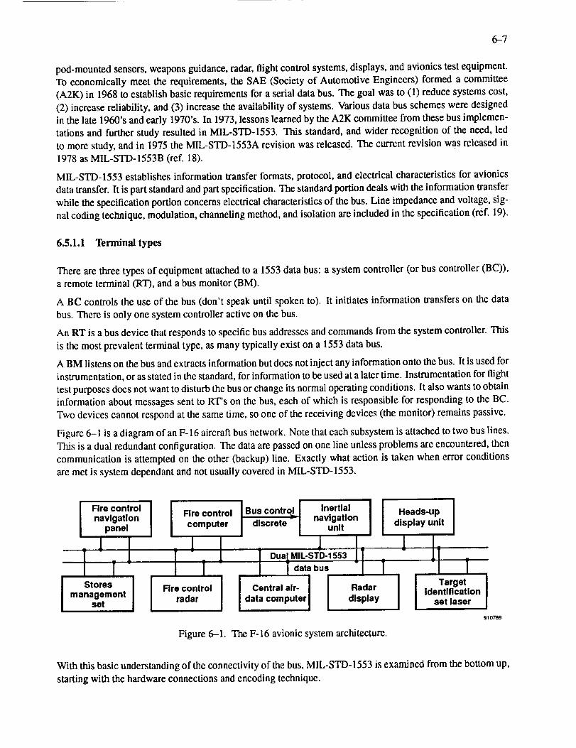
6-7
pod-mountedsensors,weaponsguidance,radar,flightcontrolsystems,displays,andavionicstestequipment.Toeconomicallymeettherequirements,theSAE(Societyof AutomotiveEngineers)formedacommittee(A2K) in 1968toestablishbasicrequirementsfor aserialdatabus.Thegoalwasto (1)reducesystemscost,(2) increasereliability,and(3) increasetheavailabilityof systems.Variousdatabusschemesweredesignedin thelate1960'sandearly1970's.In 1973,lessonslearnedbytheA2Kcommitteefromthesebusimplemen-tationsandfurtherstudyresultedin MIL-STD-1553.Thisstandard,andwiderrecognitionof theneed,ledtomorestudy,andin 1975theMIL-STD-1553Arevisionwasreleased.Thecurrentrevisionwasreleasedin1978asMIL-STD-1553B(ref.18).
MIL-STD-1553establishesinformationtransferformats,protocol,andelectricalcharacteristicsfor avionicsdatatransfer.It ispartstandardandpartspecification.Thestandardportiondealswiththeinformationtransferwhilethespecificationportionconcernselectricalcharacteristicsof thebus.Lineimpedanceandvoltage,sig-nalcodingtechnique,modulation,channelingmethod,andisolationareincludedin thespecification(ref.19).
6.5.1.1 Terminal types
There are three types of equipment attached to a 1553 data bus: a system controller (or bus controller (BC)),
a remote terminal (RT), and a bus monitor (BM).
A BC controls the use of the bus (don't speak until spoken to). It initiates information transfers on the data
bus. There is only one system controller active on the bus.
An RT is a bus device that responds to specific bus addresses and commands from the system controller. This
is the most prevalent terminal type, as many typically exist on a 1553 data bus.
A BM listens on the bus and extracts information but does not inject any information onto the bus. It is used for
instrumentation, or as stated in the standard, for information to be used at a later time. Instrumentation for flight
test purposes does not want to disturb the bus or change its normal operating conditions. It also wants to obtain
information about messages sent to RT's on the bus, each of which is responsible for responding to the BC.
Two devices cannot respond at the same time, so one of the receiving devices (the monitor) remains passive.
Figure 6-1 is a diagram of an F-16 aircraft bus network. Note that each subsystem is attached to two bus lines.
This is a dual redundant configuration. The data are passed on one line unless problems are encountered, then
communication is attempted on the other (backup) line. Exactly what action is taken when error conditions
are met is system dependant and not usually covered in MIL-STD-1553.
Fire control Inertialnavigation Fire control Bus control
panel computer discrete - navigatiOnunit
1 1 1Dual MIL-STD-1553
i i 1Stores Fire control Central alr-
management radar data computerset
TRadar
display
Figure 6-1. The F-16 avionic system architecture.
Heads-updisplay unit
1 ,T
Targetidentification
set laser
910789
With this basic understanding of the connectivity of the bus, MIL-STD-1553 is examined from the bottom up,
starting with the hardware connections and encoding technique.
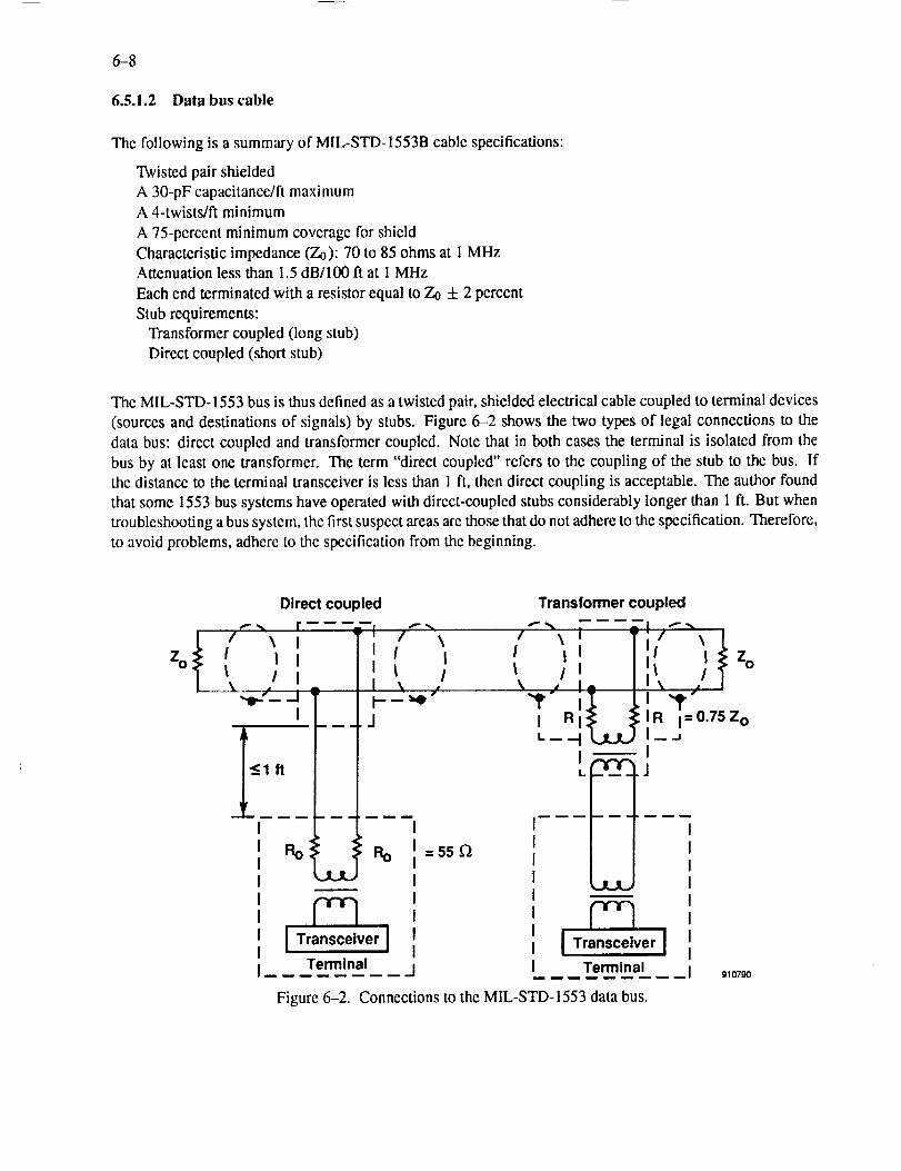
6-8
6.5.1.2 Data bus cable
The following is a summary of MIL-STD-1553B cable specifications:
Twisted pair shielded
A 30-pF capacitance/ft maximumA 4-twists/ft minimum
A 75-percent minimum coverage for shield
Characteristic impedance (Zo): 70 to 85 ohms at 1 MHzAttenuation less than 1.5 dB/100 ft at 1 MHz
Each end terminated with a resistor equal to Zo + 2 percent
Stub requirements:
Transformer coupled (long stub)
Direct coupled (short stub)
The MIL-STD-1553 bus is thus defined as a twisted pair, shielded electrical cable coupled to terminal devices
(sources and destinations of signals) by stubs. Figure 6-2 shows the two types of legal connections to the
data bus: direct coupled and transformer coupled. Note that in both cases the terminal is isolated from the
bus by at least one transformer. The term "direct coupled" refers to the coupling of the stub to the bus. Ifthe distance to the terminal transceiver is less than 1 ft, then direct coupling is acceptable. The author found
that some 1553 bus systems have operated with direct-coupled stubs considerably longer than 1 ft. But when
troubleshooting a bus system, the first suspect areas are those that do not adhere to the specification. Therefore,
to avoid problems, adhere to the specification from the beginning.
Direct coupled Transformer coupled
Zoi ;1 Ii ;
I 1 F -:'O T RII_ _ IIR Til=0.75Zo- - i__ " __;
=55
_tJL_
I ,ransce,vorITerminal J
|
I TransceiverITerminal
Figure 6-2. Connections to the MIL-STD-1553 data bus.
910790
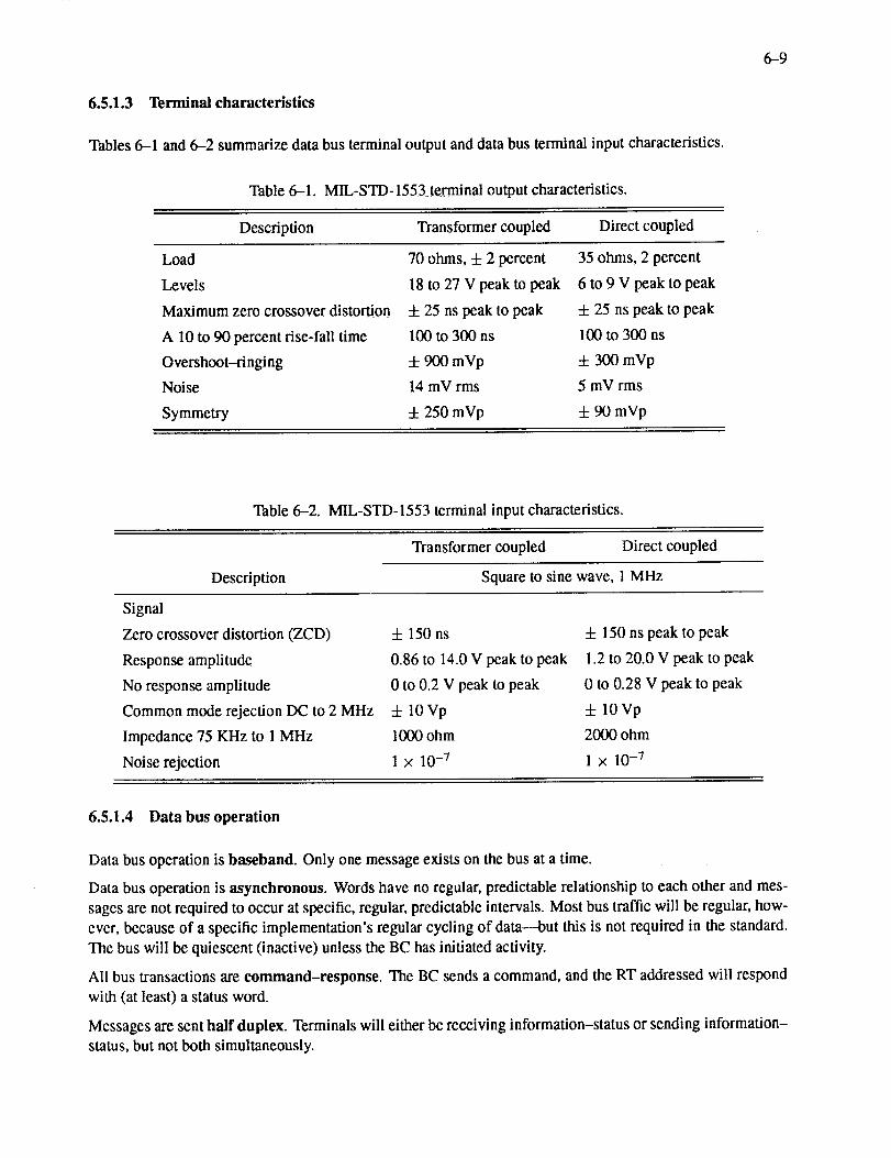
6.5.1.3 Terminal characteristics
Tables 6-1 and 6-2 summarize data bus terminal output and data bus terminal input characteristics.
Table 6-1. MIL-STD- 1553 terminal output characteristics.
6-9
Description Transformer coupled Direct coupled
Load
Levels
Maximum zero crossover distortion
A 10 to 90 percent rise-fall time
Overshoot-ringing
Noise
Symmetry
70 ohms, 4- 2 percent
18 to 27 V peak to peak
4- 25 ns peak to peak
100 to 300 ns
4- 900 mVp
14 mV rms
4- 250 mVp
35 ohms, 2 percent
6 to 9 V peak to peak
4- 25 ns peak to peak
100 to 300 ns
4- 300 mVp
5 mV rms
4- 90 mVp
Table 6-2. MIL-STD-1553 terminal input characteristics.
Description
Transformer coupled Direct coupled
Square to sine wave, 1 MHz
Signal
Zero crossover distortion (ZCD)
Response amplitude
No response amplitude
Common mode rejection DC to 2 MHz
Impedance 75 KHz to 1 MHz
Noise rejection
4- 150 ns
0.86 to 14.0 V peak to peak
0 to 0.2 V peak to peak
4- 10Vp
1000 ohm
1 x 10 -7
4- 150 ns peak to peak
1.2 to 20.0 V peak to peak
0 to 0.28 V peak to peak
4- 10Vp
2000 ohm
1 x 10⁻⁷
6.5.1.4 Data bus operation
Data bus operation is baseband. Only one message exists on the bus at a time.
Data bus operation is asynchronous. Words have no regular, predictable relationship to each other and mes-
sages are not required to occur at specific, regular, predictable intervals. Most bus traffic will be regular, how-
ever, because of a specific implementation's regular cycling of data--but this is not required in the standard.
The bus will be quiescent (inactive) unless the BC has initiated activity.
All bus transactions are command-response. The BC sends a command, and the RT addressed will respond
with (at least) a status word.
Messages are sent half duplex. Terminals will either be receiving information-status or sending information-
status, but not both simultaneously.
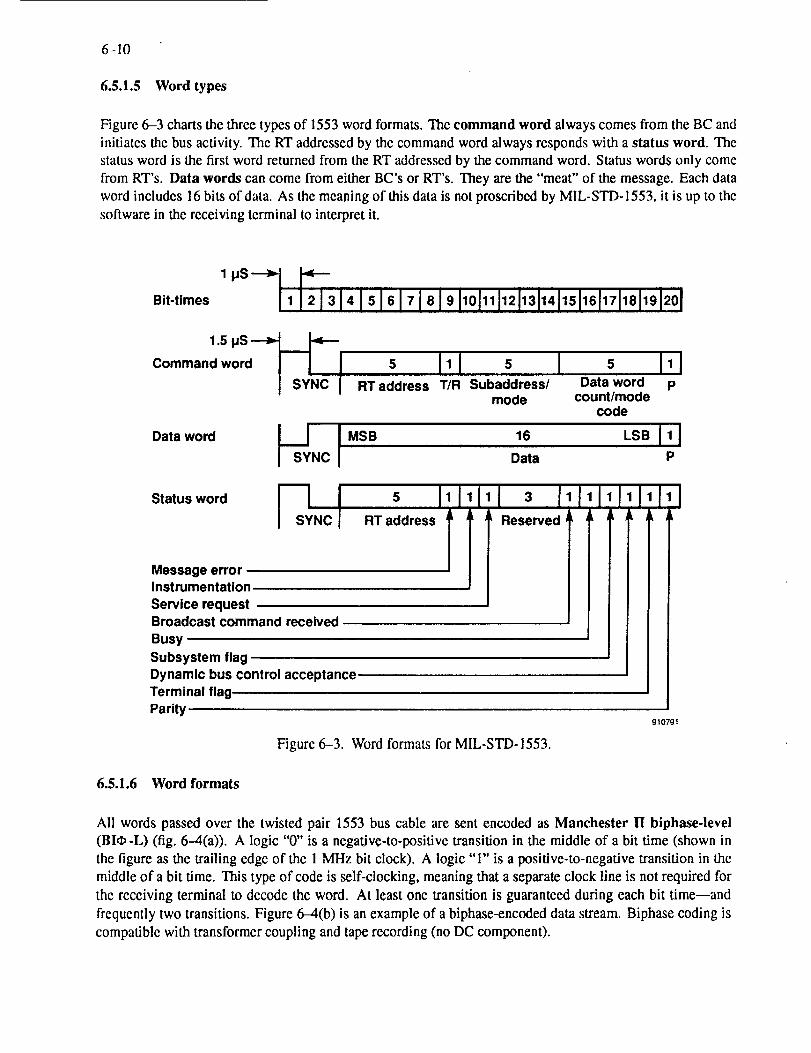
6-10
6.5.1.5 Word types
Figure 6-3 charts the three types of 1553 word formats. The command word always comes from the BC and
initiates the bus activity. The RT addressed by the command word always responds with a status word. The
status word is the first word returned from the RT addressed by the command word. Status words only come
from RT's. Data words can come from either BC's or RT's. They are the "meat" of the message. Each data
word includes 16 bits of data. As the meaning of this data is not proscribed by MIL-STD-1553, it is up to the
software in the receiving terminal to interpret it.
Bit-times 1 415161718191,01111121131141151161171181191201
1.5 pS -_ I_,_-
Command wordr----t I I [ 5 Ill s I . I,I[ SYNC RTaddress T/R Subaddress/ Data word p
mode count/modecode
Data wordI MSB ,SBI' INC Data P
Status word5 111RT address i
Message errorInstrumentation
Service requestBroadcast command received
Busy
,I,I 3 Ii _i Reserved
i
[
J
Subsystem flagDynamic bus control accelTerminal flag
ice
Parity9t07gl
Figure 6-3. Word formats for MIL-STI)-1553.
6.5.1.6 Word formats
All words passed over the twisted pair 1553 bus cable are sent encoded as Manchester II biphase-level
(BIO-L) (fig. 6-4(a)). A logic "0" is a negative-to-positive transition in the middle of a bit time (shown in
the figure as the trailing edge of the 1 MHz bit clock). A logic "1" is a positive-to-negative transition in the
middle of a bit time. This type of code is self-clocking, meaning that a separate clock line is not required for
the receiving terminal to decode the word. At least one transition is guaranteed during each bit time--and
frequently two transitions. Figure 6-4(b) is an example of a biphase-eneoded data stream. Biphase coding is
compatible with transformer coupling and tape recording (no DC component).
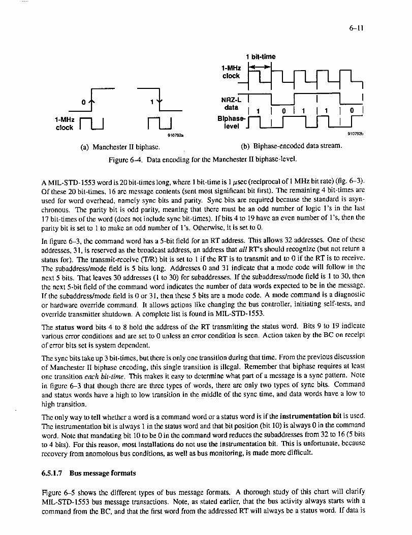
6-11
1-MHzclock
1 bit-time
1-MHz
_It NRZ-L I _ I [ I1
data 11 I 011 11 [ 0 1Blphase'r---I I I------I I---I I F--"
level J _ L-J _ ' _
g10792a 910792b
(b) Biphase-encoded data stream.
Data encoding for the Manchester II biphase-level.
(a) Manchester II biphase.
Figure 6--4.
A MIL-STD-1553 word is 20 bit-times long, where I bit-time is 1 _sec (reciprocal of 1 MHz bit rate) (fig. 6-3).
Of these 20 bit-times, 16 are message contents (sent most significant bit first). The remaining 4 bit-times are
used for word overhead, namely sync bits and parity. Sync bits are required because the standard is asyn-
chronous. The parity bit is odd parity, meaning that there must be an odd number of logic l's in the last
17 bit-times of the word (does not include sync bit-times). If bits 4 to 19 have an even number of l's, then the
parity bit is set to 1 to make an odd number of l's. Otherwise, it is set to 0.
In figure 6-3, the command word has a 5-bit field for an RT address. This allows 32 addresses. One of theseaddresses, 31, is reserved as the broadcast address, an address that all RT's should recognize (but not return a
status for). The transmit-receive (T/R) bit is set to 1 if the RT is to transmit and to 0 if the RT is to receive.
The subaddress/mode field is 5 bits long. Addresses 0 and 31 indicate that a mode code will follow in the
next 5 bits. That leaves 30 addresses (1 to 30) for subaddresses. If the subaddress/mode field is 1 to 30, then
the next 5-bit field of the command word indicates the number of data words expected to be in the message.
If the subaddress/mode field is 0 or 31, then these 5 bits are a mode code. A mode command is a diagnostic
or hardware override command. It allows a_ct_i0ns like changing the bus controller, initiating self-tests, and
override transmitter shutdown. A complete list is found in MIL-STD-1553.
The status word bits 4 to 8 hold the address of the RT transmitting the status word. Bits 9 to 19 indicate
various error conditions and are set to 0 unless an error condition is seen. Action taken by the BC on receipt
of error bits set is system dependent.
The sync bits take up 3 bit-times, but there is only one transition during that time. From the previous discussion
of Manchester II biphase encoding, this single transition is illegal. Remember that biphase requires at least
one transition each bit-time. This makes it easy to determine what part of a message is a sync pattern. Note
in figure 6-3 that though there are three types of words, there are only two types of sync bits. Command
and status words have a high to low transition in the middle of the sync time, and data words have a low to
high transition.
The only way to tell whether a word is a command word or a status word is if the instrumentation bit is used.
The instrumentation bit is always 1 in the status word and that bit position (bit 10) is always 0 in the command
word. Note that mandating bit 10 to be 0 in the command word reduces the subaddresses from 32 to 16 (5 bits
to 4 bits). For this reason, most installations do not use the instrumentation bit. This is unfortunate, because
recovery from anomolous bus conditions, as well as bus monitoring, is made more difficult.
6.5.1.7 Bus message formats
Figure 6-5 shows the different types of bus message formats. A thorough study of this chart will clarify
MIL-STD-1553 bus message transactions. Note, as stated earlier, that the bus activity always starts with a
command from the BC, and that the first word from the addressed RT will always be a status word. If data is
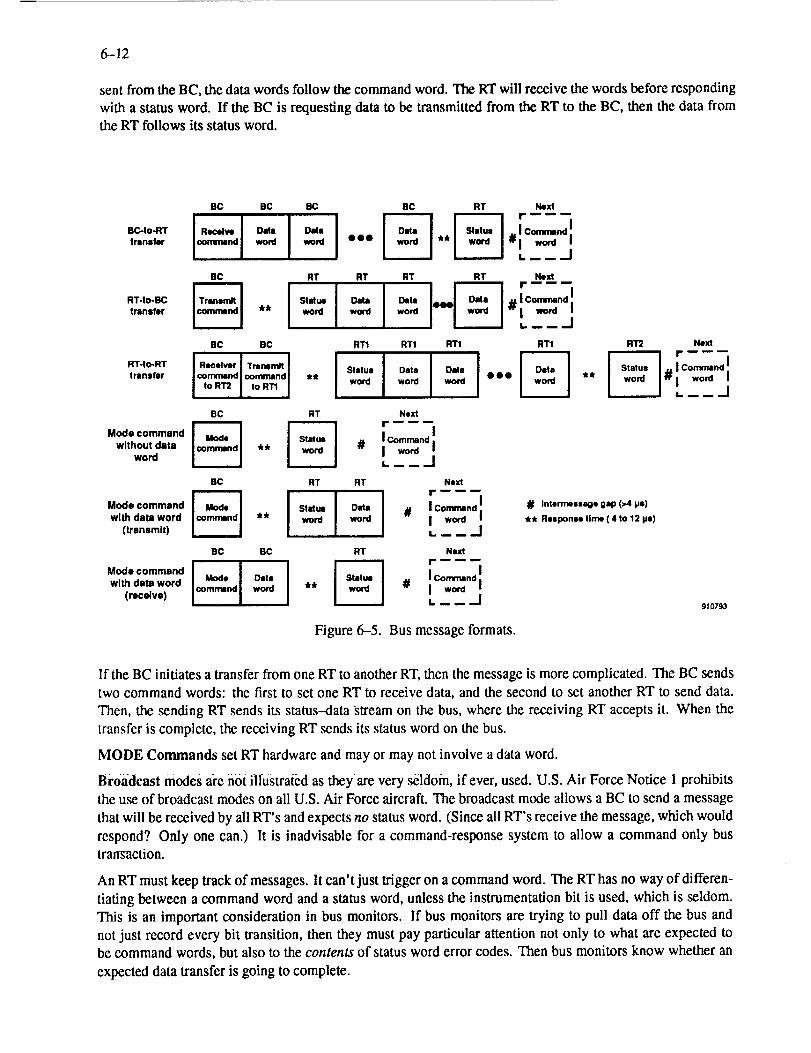
6-12
sentfromtheBC, the data words follow the command word. The RT will receive the words before responding
with a status word. If the BC is requesting data to be transmitted from the RT to the BC, then the data fromthe RT follows its status word.
BC BC BC BC RT Next
I Receive i Oltl i Datll i _ _'_ r I_:°':r_l'm"l "_ ! "_ I "'" ** +1%_"°'I. m __ --.i
BC
RT-Io-BCtransfer
RT-Io--RTtransfer
Mode command
without data
word
Mode command
with data word
(transmit)
Mode command
with data word
(receive]
RT RT RT RT Next
II l Command.
"I _ Ii-o+i i-o-i L. m __ ,_J
BC 8C RT1 RT1 RT1 RT1
I.._..,!+_..._,1 IS,at.. !°" I°" I _--]
BC RT Next
N N l Command I
** # I wo_d ,
BC RT RT Next
I+-I 0..I ',°::n°l** I +_ I "_+I + ___jBC BC RT Next
I Mode l Dala I _ '_:rn_ nd'_,,o.n,,.,,dl._ I "" # '___,
RT2 Next
is,.,,.,.,.:+::.o_ I-L__j
# Intermeesago gap ()4 ps)
,, Response time ( 4 to 12 ps)
910793
Figure 6-5. Bus message formats.
If the BC initiates a transfer from one RT to another RT, then the message is more complicated. The BC sends
two command words: the first to set one RT to receive data, and the second to set another RT to send data.
Then, the sending RT sends its status--data stream on the bus, where the receiving RT accepts it. When the
transfer is complete, the receiving RT sends its status word on the bus.
MODE Commands set RT hardware and may or may not involve a data word.
Broadcast modes are not illustrated as they are very seldom, if ever, used. U.S. Air Force Notice l prohibits
the use of broadcast modes on all U.S. Air Force aircraft. The broadcast mode allows a BC to send a message
that will be received by all RT's and expects no status word. (Since all RT's receive the message, which would
respond? Only one can.) It is inadvisable for a command-response system to allow a command only bustransaction.
An RT must keep track of messages. It can't just trigger on a command word. The RT has no way of differen-
tiating between a command word and a status word, unless the instrumentation bit is used, which is seldom.
This is an important consideration in bus monitors. If bus monitors are trying to pull data off the bus and
not just record every bit transition, then they must pay particular attention not only to what are expected tobe command words, but also to the contents of status word error codes. Then bus monitors know whether an
expected data transfer is going to complete.
6-13
6.5.1.8 MIL-STD-1553 notices
The 1553 standard has been revised in the form of "Notices." Notices can be thought of as implementation
practices desired or mandated by certain organizations. Notice 1 puts several limitations on the MIL-STD-
1553B standard. Whereas the standard permits switching of a bus controller (by use of a mode command),
Notice 1 does not. The standard defines a broadcast mode; Notice 1 says not to use it. The standard allows a
single bus, or multiple redundant buses; the Notice specifies that all implementations shall be dual redundant.
The Notice also points out the differences between MIL-STD-1553A and MIL-STD-1553B and tightens cable
characteristics (impedance and shielding).
There is a Notice 2 that further defines some timing variables implied within the standard. Options are described
in the area of status word bits, mode codes, data bus redundancy, and coupling techniques. Notice 2 is generally
observed outside the U.S. and is reflected in STANAG 3838, which is a NATO document that includes 1553within it.
6.5.1.9 Design tips for MIL-STD-1553.
When any standard has different versions, some level of incompatibility is introduced. This is the case with
the two prevalent 1553 standards: MIL-STD-1553A and MIL-STD-1553B. Another version that differs from
both the A and B revisions is found on some aircraft, notably the McDonnell Douglas F-18 aircraft. In flight
test instrumentation work, where retrofitting and multiple aircraft types are instrumented, an understanding
of the potential problems (pitfalls) in mixing different revision compliant equipment is important. The most
common difference is in expected response time after a message is passed.
It is extremely important for a flight test instrumentation engineer to understand the limitations of the
MIL-STD-1553 data bus. There are classes of signals that are considered inappropriate for 1553 commu-nications. These are:
1. High signal bandwidth data (single signals above 400 Hz) like FM and video.
2. Signals used to control startup of the system prior to initialization of the 1553 systeml
3. Backup signals that are required for safety of flight if complete 1553 system failure occurs.
The most important of these classes from a flight test instrumentation (FTI) engineer's standpoint is high signal
bandwidth data. In flight research work, highly regular, high-data-rate requirements do not work well when
passed through a 1553 bus.
Many flight test activities involve development of avionics systems. In these tests, it is important to analyze
all of the bus activity, including the timing and message gaps. This generally cannot be done in real time, so
a requirement for recording the bus traffic is generated. Unfortunately, the protocol used effectively to pass
messages on the bus presents difficulties in data analysis. Remember that the analyst may be interested in more
than the contents of the data packets. A way must be found to encode the bus timing information as well as the
data. A further complication is that the 1-Mblt/sec 1553 data rate is too fast for most conventional recording
mechanisms. Also, as many as six separate 1553 data buses must be recorded. A variety of recording tech-
niques have been developed. The most common technique is called track splitting. A single stream coming in
from a 1553 bus is split across several tracks, allowing the bit rate of each tape channel to be reduced. However,
this technique requires several decommutators to reconstruct the original data flow from one data bus, and if
one tape track has problems, it affects the whole message. Use of new wideband tape recorders allow a single
1553 bus data flow to be recorded on one tape track. To facilitate data extraction from the tape, it is a common
practice to synchronize the data before it is recorded. This is accomplished by creating a data stream that has
no "inactive" time and includes synchronization words. In some systems, timing checks are done on the bus
and illegal separations or other bus errors cause error words to be set and recorded on tape along with the data.
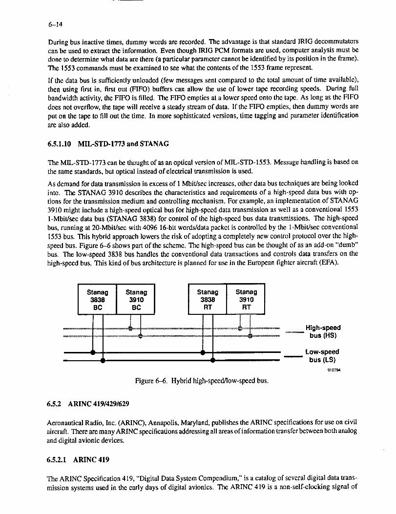
6-14
Duringbusinactivetimes,dummywordsarerecorded.Theadvantageis thatstandardIRIGdecommutatorscanbeusedtoextracttheinformation.EventhoughIRIGPCMformatsareused,computeranalysismustbedonetodeterminewhatdataarethere(aparticularparametercannotbeidentifiedby itspositionin theframe).The1553commandsmustbe examined to see what the contents of the 1553 frame represent.
If the data bus is sufficiently unloaded (few messages sent compared to the total amount of time available),
then using first in, first out (FIFO) buffers can allow the use of lower tape recording speeds. During full
bandwidth activity, the FIFO is filled. The FIFO empties at a lower speed onto the tape. As long as the FIFO
does not overflow, the tape will receive a steady stream of data. If the FIFO empties, then dummy words are
put on the tape to fill out the time. In more sophisticated versions, time tagging and parameter identificationare also added.
6.5.1.10 MIL-STD-1773 and STANAG
The MIL-STD-1773 can be thought of as an optical version of MIL-STD-1553. Message handling is based on
the same standards, but optical instead of electrical transmission is used.
As demand for data transmission in excess of 1 Mbit/sec increases, other data bus techniques are being looked
into. The STANAG 3910 describes the characteristics and requirements of a high-speed data bus with op-
tions for the transmission medium and controlling mechanism. For example, an implementation of STANAG
3910 might include a high-speed optical bus for high-speed data transmission as well as a conventional 1553
1-Mbit/sec data bus (STANAG 3838) for control of the high-speed bus data transmissions. The high-speed
bus, running at 20-Mbit/sec with 4096 16-bit words/data packet is controlled by the l-Mbit/sec conventional
1553 bus. This hybrid approach lowers the risk of adopting a completely new control protocol over the high.
speed bus. Figure 6-6 shows part of the scheme. The high-speed bus can be thought of as an add-on "dumb"
bus. The low-speed 3838 bus handles the conventional data transactions and controls data transfers on the
high-speed bus. This kind of bus architecture is planned for use in the European fighter aircraft (EFA).
Stanag3838BC
Stanag Stanag Stanag3910 3838 3910BC RT RT
! l i..... _ ...... _,,_,_, High-speed
............. __ ..... -_ _,,_---_--- bus (HS)
,L ----- Low-speed•----- bus (LS)
910794
Figure 6--6. Hybrid high-speed/low-speed bus.
6.5.2 ARINC 419/429/629
Aeronautical Radio, Inc. (ARINC), Annapolis, Maryland, publishes the ARINC specifications for use on civil
aircraft. There are many ARINC specifications addressing all areas of information transfer between both analog
and digital avionic devices.
6.5.2.1 ARINC 419
The ARINC Specification 419, "Digital Data System Compendium," is a catalog of several digital data trans-
mission systems used in the early days of digital avionics. The ARINC 419 is a non-self-clocking signal of
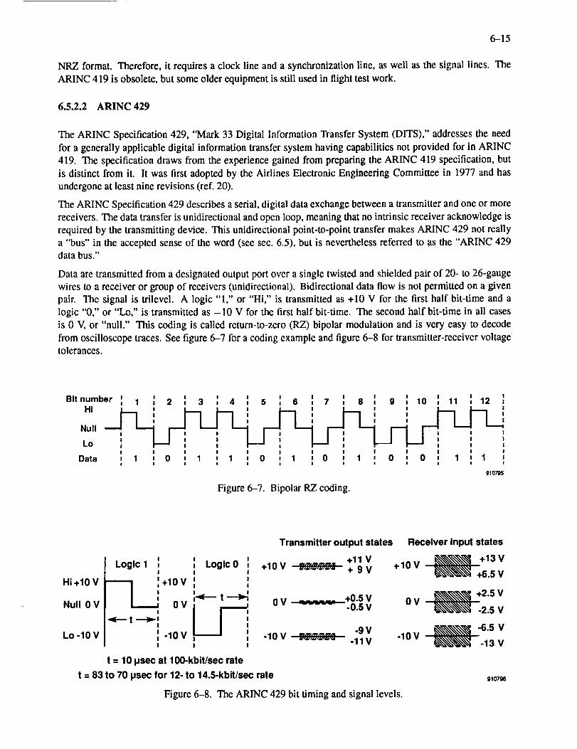
6-15
NRZformat.Therefore,it requires a clock line and a synchronization line, as well as the signal lines. The
ARINC 419 is obsolete, but some older equipment is still used in flight test work.
6.5.2.2 ARINC 429
The ARINC Specification 429, "Mark 33 Digital Information Transfer System (DITS)," addresses the need
for a generally applicable digital information transfer system having capabilities not provided for in ARINC
419. The specification draws from the experience gained from preparing the ARINC 419 specification, but
is distinct from it. It was first adopted by the Airlines Electronic Engineering Committee in 1977 and has
undergone at least nine revisions (ref. 20).
The ARINC Specification 429 describes a serial, digital data exchange between a transmitter and one or more
receivers. The data transfer is unidirectional and open loop, meaning that no intrinsic receiver acknowledge is
required by the transmitting device. This unidirectional point-to-point transfer makes ARINC 429 not really
a "bus" in the accepted sense of the word (see sec. 6.5), but is nevertheless referred to as the "ARINC 429data bus."
Data are transmitted from a designated output port over a single twisted and shielded pair of 20- to 26-gauge
wires to a receiver or group of receivers (unidirectional). Bidirectional data flow is not permitted on a given
pair. The signal is trilevel. A logic "1," or "Hi," is transmitted as +10 V for the first half bit-time and a
logic "0," or "Lo," is transmitted as -10 V for the first half bit-time. The second half bit-time in all cases
is 0 V, or "null." This coding is called return-to-zero (RZ) bipolar modulation and is very easy to decode
from oscilloscope traces. See figure 6-7 for a coding example and figure 6-8 for transmitter-receiver voltagetolerances.
I I I I I I I I I I [ I IBit number _ 1 J 2 , 3 , 4 . 5 _ 6 , 7 = 8 , 9 , 10 . 11 , 12, , t---1 I--'1NI ', ' ' I I I I i
Null "--"! I
Lo i I I ' II I I II i, . . i . i J . i i I ,
Data I 1 , 0 , 1 ' 1 ' 0 i 1 i 0 , 1 ' 0 J 0 , 1 ' 1i i i i i ! , i i ! l i
g107_5
Figure 6-7. Bipolar RZ coding.
Hi+10 V
Null 0 V
Lo -10 V
Logic 1
-_+10VOV
I
!
' -10 VII
ILogic 0
IIII
_S
Transmitter output states Receiver Input states
.11 V _._ .13V+10 V '"-":'_"-: + 9 V + 10 V _'_'_'_ +6.5 V
0V _+0.5V 0V _,._ +2.5V-0.5 V _'_'_'_ -2.5 V
-9 V _%--_'_ -6.5 V-10V :',_".3"._:: -11V -10V _;="_'_'_ -13 V
t = 10 psec at lO0-kbit/sec rate
t = 83 to 70 psec for 12- to 14.5-kbit/sec rate
Figure 6-8. The ARINC 429 bit timing and signal levels.
g10796
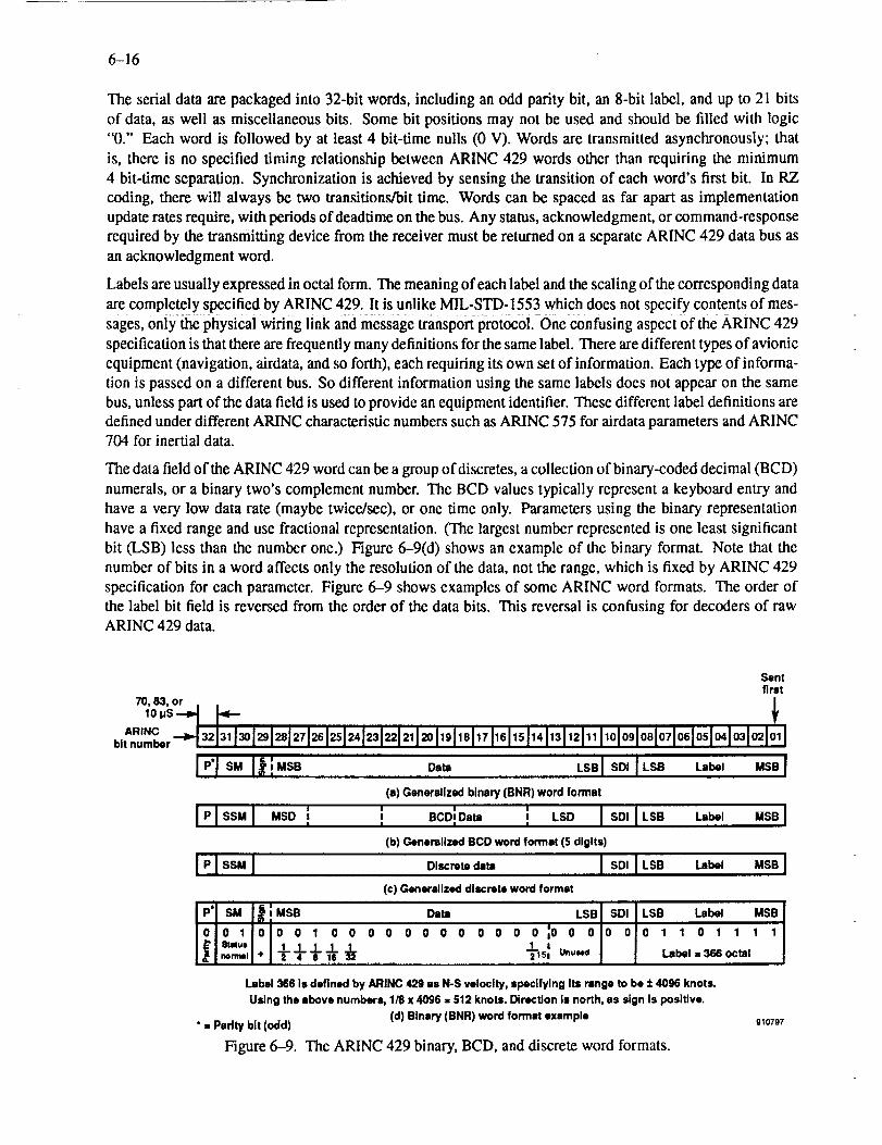
6-16
The serial data are packaged into 32-bit words, including an odd parity bit, an 8-bit label, and up to 21 bits
of data, as well as miscellaneous bits. Some bit positions may not be used and should be filled with logic
"0." Each word is followed by at least 4 bit-time nulls (0 V). Words are transmitted asynchronously; that
is, there is no specified timing relationship between ARINC 429 words other than requiring the minimum
4 bit-time separation. Synchronization is achieved by sensing the transition of each word's first bit. In RZ
coding, there will always be two transitions/bit time. Words can be spaced as far apart as implementation
update rates require, with periods ofdeadtime on the bus. Any status, acknowledgment, or command-response
required by the transmitting device from the receiver must be returned on a separate ARINC 429 data bus as
an acknowledgment word.
Labels are usually expressed in octal form. The meaning of each label and the scaling of the corresponding data
are completely specified by ARINC 429. It is unlike MIL-STD-1553 which does not specify contents of mes-
sages, only_the physical wiring link and message transport protocol. One confusing aspect of the ARINC 429
specification is that there are frequently many definitions for the same label. There are different types of avionic
equipment (navigation, alrdata, and so forth), each requiring its own set of information. Each type of informa-
tion is passed on a different bus. So different information using the same labels does not appear on the same
bus, unless part of the data field is used to provide an equipment identifier. These different label definitions are
defined under different ARINC characteristic numbers such as ARINC 575 for airdata parameters and ARINC
704 for inertial data.
The data field of the ARINC 429 word can be a group ofdiscretes, a collection of binary-coded decimal (BCD)
numerals, or a binary two's complement number. The BCD values typically represent a keyboard entry and
have a very low data rate (maybe twice/sec), or one time only. Parameters using the binary representation
have a fixed range and use fractional representation. (The largest number represented is one least significant
bit (LSB) less than the number one.) Figure 6-9(d) shows an example of the binary format. Note that the
number of bits in a word affects only the resolution of the data, not the range, which is fixed by ARINC 429
specification for each parameter. Figure 6-9 shows examples of some ARINC word formats. The order of
the label bit field is reversed from the order of the data bits. This reversal is confusing for decoders of rawARINC 429 data.
Sentfirst
70, 83, or /
,o.sZflt*-AR,NC- 13213,I o/ ,1 !2?12sl2,12,1 1,.I 120t,,t,sl,,11611s114ball21,1,01-1o,Ho lo,lo,lo lo lo,I
bitnumoer_ t...J_ i i i
I¢1s. I i.s. ,s.I be. .,s.I(a) Generalized binary (BNR) word format
l Iss"I .so i i .co!o.- i LSOIsD, La -' I(b) Generalized BCD word format (S digits)
! P I SSM I Discrete date I SDI I LSB Label MSB !
(c) C,enerallzed discrata word format
P" SM _j MSB Dam LS. SDI,,, LSB Label MSB
0 0 1 0 0 0 1 0 0 0 0 0 0 0 0 0 0 0 0:0 0 0 0 0 0 1 1 0 1 1 1 I
8lalul I Ir_rml + "_ 4J" "_- "_" "_ TlS, Unused Label = 366 octal
Label 366 Is defined by ARINC 429 as N-S velocity, specifying Its range to be + 4096 knots.
Using the above numbers, 1/8 x 4096 ,, 512 knots. Direction is north, as sign Is positive.
(d) Binary (BNR) word format example" = Psdty bit (odd) 910797
Figure 6-9. The ARINC 429 binary, BCD, and discrete word formats.
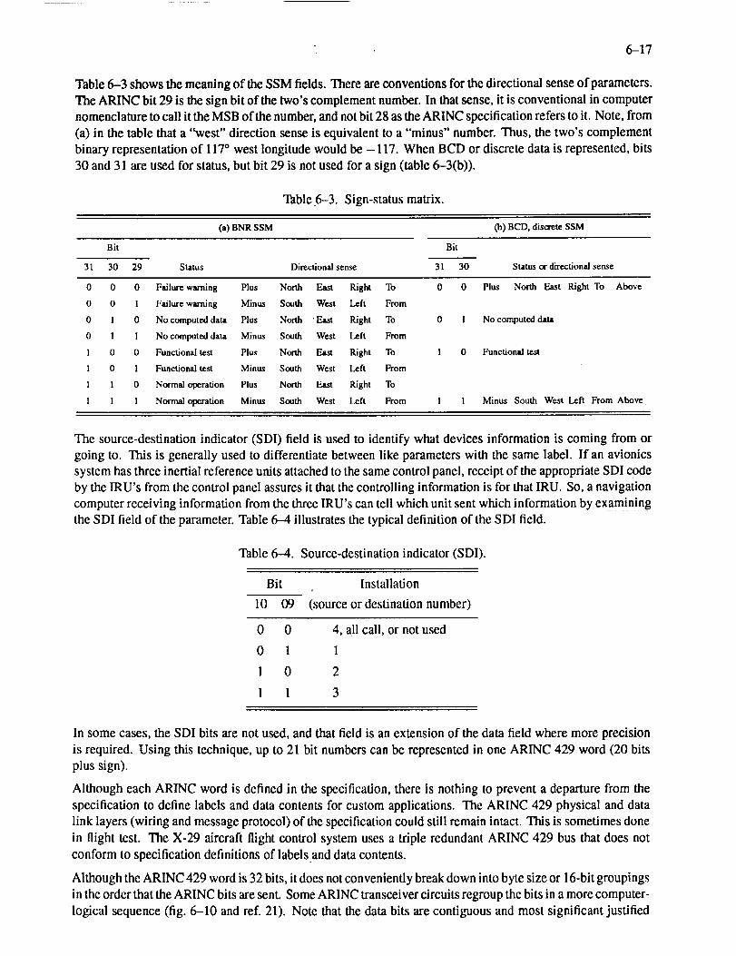
6-17
Table6-3showsthemeaningof theSSMfields. There are conventions for the directional sense of parameters.
The ARINC bit 29 is the sign bit of the two's complement number. In that sense, it is conventional in computer
nomenclature to call it the MSB of the number, and not bit 28 as the ARINC specification refers to it. Note, from
(a) in the table that a "west" direction sense is equivalent to a "minus" number. Thus, the two's complement
binary representation of 117 ° west longitude would be - 117. When BCD or discrete data is represented, bits
30 and 31 are used for status, but bit 29 is not used for a sign (table 6-3(b)).
Table 6-3. Sign-status matrix.
(a) BNR SSM
Bit Bit
0a) BCD, disca'ete SSM
31 30 29 Status Directional sense 31 30 Status ot directional sense
0 0 0 Failure warning Plus North East Right To 0 0 Plus North East Right To Above
0 0 1 Failure warning Minus South West Left From
0 1 0 No computed data Plus North "East Right To 0 i No computed data
0 1 1 No computed data Minus South West Left From
I 0 0 Functional test Plus North East Right To ! 0 Functional test
1 0 i Functional test Minus South West Left From
1 1 0 Normal operation Plus North East Right To
1 1 1 Normal operation Minus South West Left From 1 1 Minus South West Left From Above
The source-destination indicator (SDI) field is used to identify what devices information is coming from or
going to. This is generally used to differentiate between like parameters with the same label. If an avionics
system has three inertial reference units attached to the same control panel, receipt of the appropriate SDI code
by the IRU's from the control panel assures it that the controlling information is for that IRU. So, a navigation
computer receiving information from the three IRU's can tell which unit sent which information by examining
the SDI field of the parameter. Table 6-4 illustrates the typical definition of the SDI field.
Table 6-4. Source-destination indicator (SDI).
Bit Installation
10 09 (source or destination number)
0 0 4, all call, or not used
0 1 1
1 0 2
l I 3
In some cases, the SDI bits are not used, and that field is an extension of the data field where more precision
is required. Using this technique, up to 21 bit numbers can be represented in one ARINC 429 word (20 bits
plus sign).
Although each ARINC word is defined in the specification, there is nothing to prevent a departure from the
specification to define labels and data contents for custom applications. The ARINC 429 physical and data
link layers (wiring and message protocol) of the specification could still remain intact. This is sometimes done
in flight test. The X-29 aircraft flight control system uses a triple redundant ARINC 429 bus that does not
conform to specification definitions of labels and data contents.
Although the ARINC 429 word is 32 bits, it does not conveniently break down into byte size or 16-bit groupings
in the order that the ARINC bits are sent. Some ARINC transceiver circuits regroup the bits in a more computer-
logical sequence (fig. 6-10 and ref. 21). Note that the data bits are contiguous and most significant justified
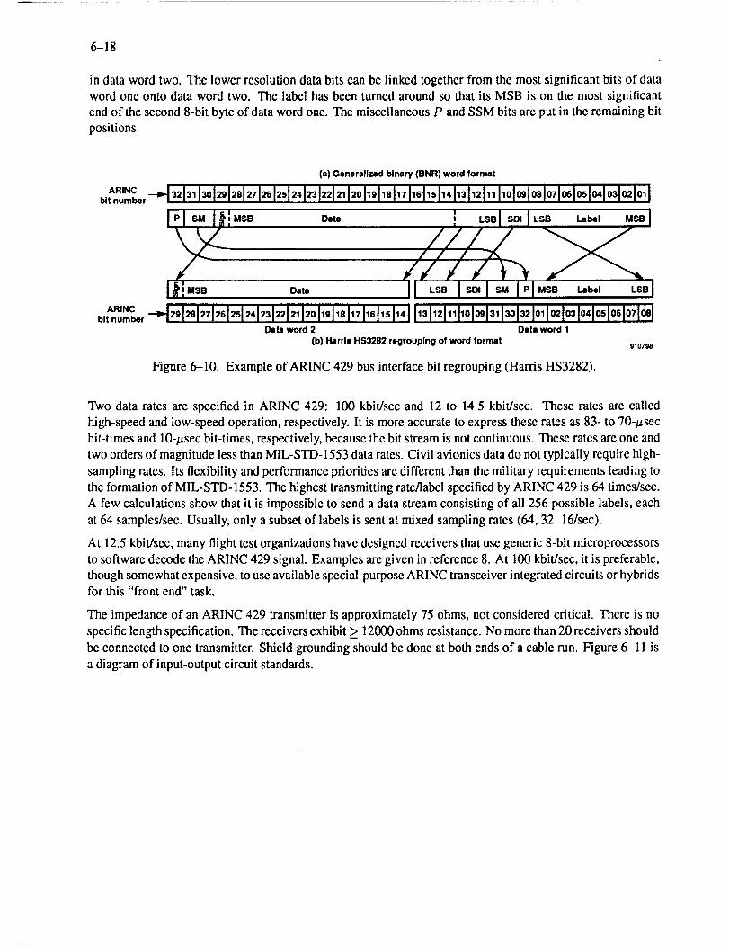
6-18
in data word two. The lower resolution data bits can be linked together from the most significant bits of data
word one onto data word two. The label has been turned around so that its MSB is on the most significant
end of the second 8-bit byte of data word one. The miscellaneous P and SSM bits are put in the remaining bit
positions.
(a) Generalized binary (BNR) word format
, .".'"_L.--1321311 !=,12812,1= 12512,12312212,120I1,1,01,,Ils1, 1,4I b l-11olo81o.Ho81o51o,Io31o21o,Ibit Ilglll_l II II Ill I i IIIIII
Data
DataI
ARINCbltnumber 29 28 27 26 25 24 23 22 21 20 19 18 17 16 15 14 13 12 11 10 09 31 30 32 01 02 03 04 05 O6 O7 O8
Data word 2 Data word 1(b) Harris HS3282 regrouplng of word format
910798
Figure 6-10. Example of ARINC 429 bus interface bit regrouping (Harris HS3282).
Two data rates are specified in ARINC 429:100 kbit/sec and 12 to 14.5 kbit/sec. These rates are called
high-speed and low-speed operation, respectively. It is more accurate to express these rates as 83- to 70-/zsec
bit-times and 10-ttsec bit-times, respectively, because the bit stream is not continuous. These rates are one and
two orders of magnitude less than MIL-STD-1553 data rates. Civil avionics data do not typically require high-
sampling rates. Its flexibility and performance priorities are different than the military requirements leading to
the formation of MIL-STD-1553. The highest transmitting rate/label specified by ARINC 429 is 64 times/sec.
A few calculations show that it is impossible to send a data stream consisting of all 256 possible labels, each
at 64 samples/sec. Usually, only a subset of labels is sent at mixed sampling rates (64, 32, 16lsec).
At 12.5 kbit/sec, many flight test organizations have designed receivers that use generic 8-bit microprocessors
to software decode the ARINC 429 signal. Examples are given in reference 8. At 100 kbit/sec, it is preferable,
though somewhat expensive, to use available special-purpose ARINC transceiver integrated circuits or hybridsfor this "front end" task.
The impedance of an ARINC 429 transmitter is approximately 75 ohms, not considered critical. There is no
specific length specification. The receivers exhibit _> 12000 ohms resistance. No more than 20 receivers should
be connected to one transmitter. Shield grounding should be done at both ends of a cable run. Figure 6-11 is
a diagram of input-output circuit standards.
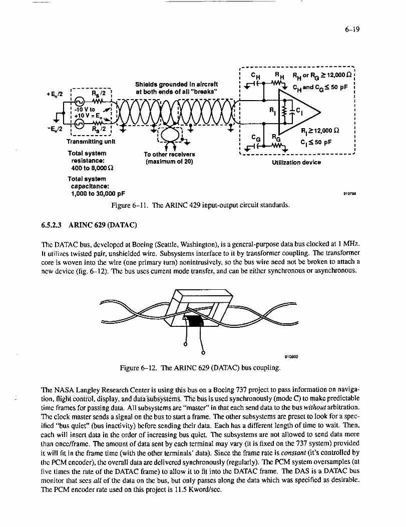
6-19
nwuwll mDmm_l wl_wlnmn_wwm,
C H R H RH or RG-> 12,000_
Shields grounded in aircraft _¢-I __ C_ and CG_ 50 pF+ Eo/2 [ Rs/2 =, at both ends of all "breaks" [ L'--,.:
..... ----; i 1 CG RG 'Transmitting unit t_'__. _C:_I_ C1<_50 pFTotal system To other receivers
resistance: (maximum of 20) Utilization device400 to 8,000
Total systemcapacitance:1,000 to 30,000 pF 910r_
Figure 6-11. The ARINC 429 input-output circuit standards.
6.5.2.3 ARINC 629 (DATAC)
The DATAC bus, developed at Boeing (Seattle, Washington), is a general-purpose data bus clocked at 1 MHz,
It utilizes twisted pair, unshielded wire. Subsystems interface to it by transformer coupling. The transformer
core is woven into the wire (one primary turn) nonintrusively, so the bus wire need not be broken to attach a
new device (fig. 6-12). The bus uses current mode transfer, and can be either synchronous or asynchronous.
910800
Figure 6-12. The ARINC 629 (DATAC) bus coupling.
The NASA Langley Research Center is using this bus on a Boeing 737 project to pass information on naviga-
tion, flight control, display, and data subsystems. The bus is used synchronously (mode C) to make predictable
time frames for passing data. All subsystems are "master" in that each send data to the bus without arbitration.
The clock master sends a signal on the bus to start a frame. The other subsystems are preset to look for a spec-
ified "bus quiet" (bus inactivity) before sending their data. Each has a different length of time to wait. Then,
each will insert data in the order of increasing bus quiet. The subsystems are not allowed to send data more
than once/frame. The amount of data sent by each terminal may vary (it is fixed on the 737 system) provided
it will fit in the frame time (with the other terminals' data). Since the frame rate is constant (it's controlled by
the PCM encoder), the overall data are delivered synchronously (regularly). The PCM system oversamples (at
five times the rate of the DATAC frame) to allow it to fit into the DATAC frame. The DAS is a DATAC bus
monitor that sees all of the data on the bus, but only passes along the data which was specified as desirable.
The PCM encoder rate used on this project is 11.5 Kword/sec.
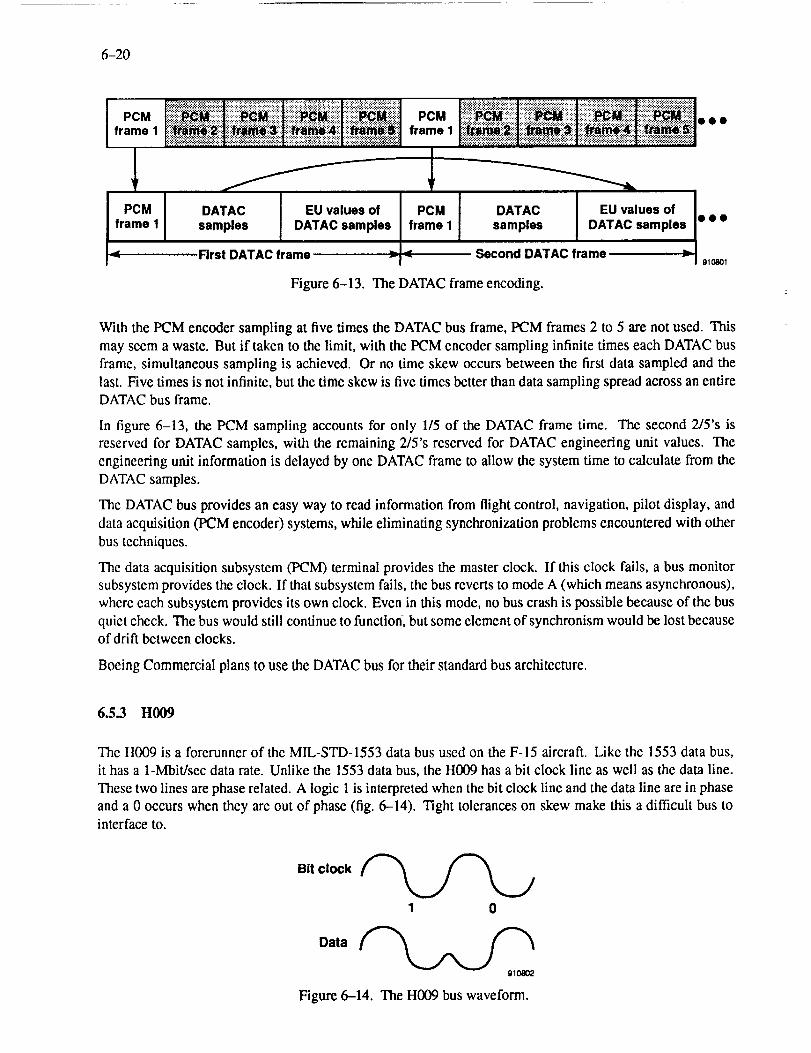
6-20
,°. iiii',ii aii!i,c..frame
frame I ii::i_iii_iiiiiii!!i_iii::i_iii:_i_2_i!iii!ii:::,_i!iiii!!!!iii':ii':i::iii::i::ii!ii:,::ii::i:,ii':_ii_iiii_!ii_i
PCM DATAC EU values of PCMframe I samples DATAC samples frame 1
-" First DAT/__""..........
oee
DATAC EU values of • • •samples DATAC samples
_,,..,_I r_'IrA_ #_.-,_,_, ] 910801
Figure 6-13. The DATAC frame encoding.
With the PCM encoder sampling at five times the DATAC bus frame, PCM frames 2 to 5 are not used. This
may seem a waste. But if taken to the limit, with the PCM encoder sampling infinite times each DATAC bus
frame, simultaneous sampling is achieved. Or no time skew occurs between the first data sampled and the
last. Five times is not infinite, but the time skew is five times better than data sampling spread across an entireDATAC bus frame.
In figure 6-13, the PCM sampling accounts for only 1/5 of the DATAC frame time. The second 2/5's is
reserved for DATAC samples, with the remaining 2/5's reserved for DATAC engineering unit values. The
engineering unit information is delayed by one DATAC frame to allow the system time to calculate from the
DATAC samples.
The DATAC bus provides an easy way to read information from flight control, navigation, pilot display, and
data acquisition (PCM encoder) systems, while eliminating synchronization problems encountered with other
bus techniques.
The data acquisition subsystem (PCM) terminal provides the master clock. If this clock fails, a bus monitor
subsystem provides the clock. If that subsystem fails, the bus reverts to mode A (which means asynchronous),
where each subsystem provides its own clock. Even in this mode, no bus crash is possible because of the bus
quiet check. The bus would still continue to function, but some element of synchronism would be lost becauseof drift between clocks.
Boeing Commercial plans to use the DATAC bus for their standard bus architecture.
6.5.3 H009
The H009 is a forerunner of the MIL-STD-1553 data bus used on the F-15 aircraft. Like the 1553 data bus,
it has a 1-Mbit/sec data rate. Unlike the 1553 data bus, the H009 has a bit clock line as well as the data line.
These two lines are phase related. A logic 1 is interpreted when the bit clock line and the data line are in phase
and a 0 occurs when they are out of phase (fig. 6-14). Tight tolerances on skew make this a difficult bus tointerface to.
Bit clock
1 0
Data910802
Figure 6-14. The H009 bus waveform.
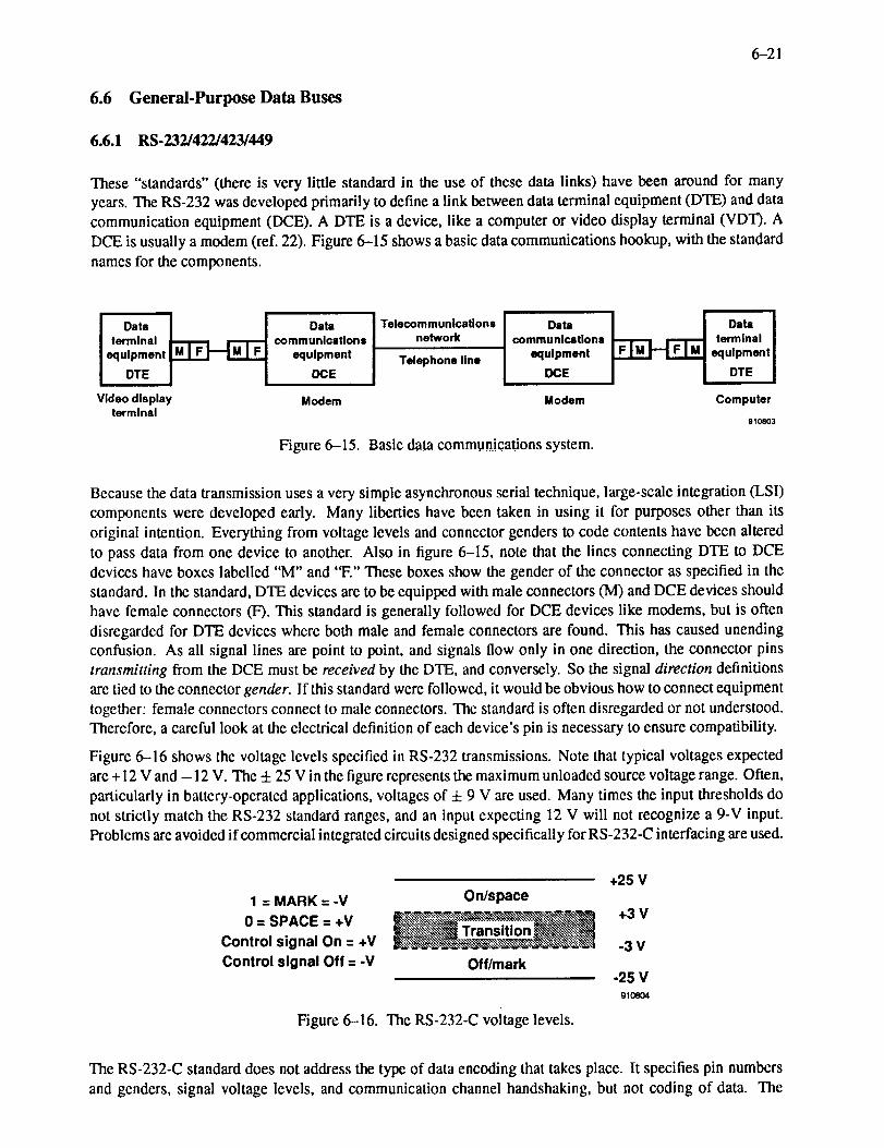
6-21
6.6 General-Purpose Data Buses
6.6.1 RS-232/422/423/449
These "standards" (there is very little standard in the use of these data links) have been around for many
years. The RS-232 was developed primarily to define a link between data terminal equipment (DTE) and data
communication equipment (DCE). A DTE is a device, like a computer or video display terminal (VDT). A
DCE is usually a modem (ref. 22). Figure 6-15 shows a basic data communications hookup, with the standard
names for the components.
Dataterminal
equipment
DTEi
Video displayterminal
Datacommunications
equipment
DCE
Telecommunicationsnetwork
Telephone line
Datacommunications
equipment
DCE
Modem Modem
Figure 6-15. Basic data communications system.
Dataterminal
equipment
DTE
Computer
910803
Because the data transmission uses a very simple asynchronous serial technique, large-scale integration (LSI)
components were developed early. Many liberties have been taken in using it for purposes other than its
original intention. Everything from voltage levels and connector genders to code contents have been altered
to pass data from one device to another. Also in figure 6-15, note that the lines connecting DTE to DCE
devices have boxes labelled "M" and "F." These boxes show the gender of the connector as specified in the
standard. In the standard, DTE devices are to be equipped with male connectors (M) and DCE devices should
have female connectors (F). This standard is generally followed for DCE devices like modems, but is often
disregarded for DTE devices where both male and female connectors are found. This has caused unending
confusion. As all signal lines are point to point, and signals flow only in one direction, the connector pins
transmitting from the DCE must be received by the DTE, and conversely. So the signal direction definitions
are tied to the connector gender. If this standard were followed, it would be obvious how to connect equipment
together: female connectors connect to male connectors. The standard is often disregarded or not understood.
Therefore, a careful look at the electrical definition of each device's pin is necessary to ensure compatibility.
Figure 6-16 shows the voltage levels specified in RS-232 transmissions. Note that typical voltages expected
are + 12 V and - 12 V. The -1-25 V in the figure represents the maximum unloaded source voltage range. Often,
particularly in battery-operated applications, voltages of -1-9 V are used. Many times the input thresholds do
not strictly match the RS-232 standard ranges, and an input expecting 12 V will not recognize a 9-V input.
Problems are avoided if commercial integrated circuits designed specifically for RS-232-C interfacing are used.
1 = MARK = -V
0 = SPACE = +V
Control signal On = +V
Control signal Off = -V
On/space
Off/mark
Figure 6-16. The RS-232-C voltage levels.
+25 V
+3 V
-3 V
-25 V910804
The RS-232-C standard does not address the type of data encoding that takes place. It specifies pin numbers
and genders, signal voltage levels, and communication channel handshaking, but not coding of data. The
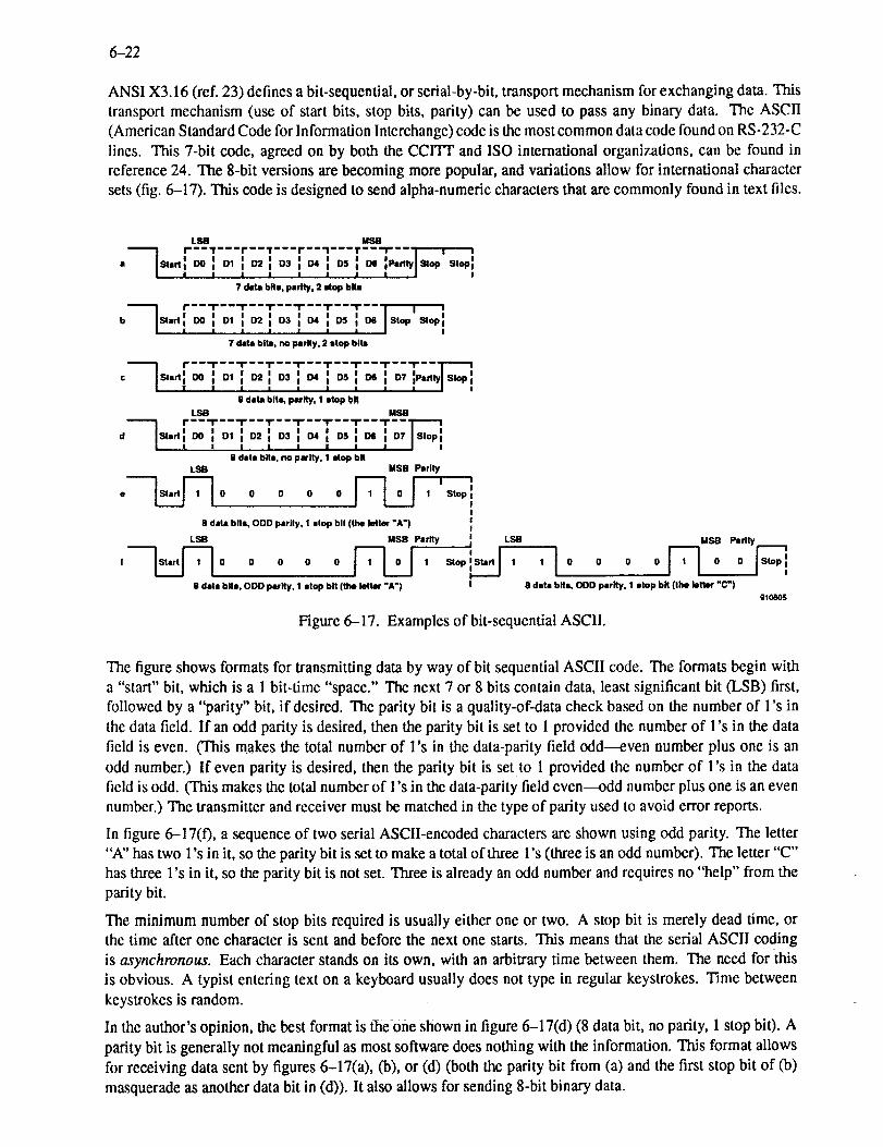
6-22
ANSIX3.16(re/'.23)definesabit-sequential,orserial-by-bit,transportmechanismforexchangingdata.Thistransportmechanism(useof startbits,stopbits,parity)canbeusedto passanybinarydata. TheASCII(AmericanStandardCodeforInformationInterchange)codeisthemostcommondatacodefoundonRS-232-Clines.This7-bit code,agreedonby boththeCCITTandISOinternationalorganizations,canbe found in
reference 24. The 8-bit versions are becoming more popular, and variations allow for international character
sets (fig. 6-17). This code is designed to send alpha-numeric characters that are commonly found in text files.
LSB MSB
"--I r'" l"--r-- l"'-r'''l--- T'-'v''" i _ ,I I I I I I I ; !
• [Sisd I DO I D1 I D2 I D3 1 D4 I 05 I D6 stop,! ' ' I I i , , i i I
7 data bill, parib/, 2 MOp bitl
i" -- -- " " -- " -- -- " -- -- " -- -- " -- -- " -- --iI i i i ' I _Op :'oo:o,. 1°'1o.: : st.'7 data bits, no parity, 2 stop bits
I I I I I l I I I I_Is,.,,, oo , m , _, 03 . a. , .s , _ , D_,Pa._Is_:i =
1 • ! i l l I ! l a l I
8 data bits, parHy, 1 stop bit
LS8 MSB
d
8 data bits, no parity, 1 Mop bitLSB MSB Parity
• 0 0 0 0 0 1 Stop
8 dals bits, ODD parity, 1 slop bit (the ieltm' "A")
LSB MSB Parity LSB
i St-___0 0 0 0 0 _.__ 1 Stop :S_t._ 1 :1 0 0 0
8 dais bits, ODD parity, 1 stop bit (the kl4t_ "A') I 8 data bits, ODD parity, 1 stop bit {the bttor "C')
MS8 Parity
0J o
Figure 6-17. Examples of bit-sequential ASCII.
The figure shows formats for transmitting data by way of bit sequential ASCII code. The formats begin with
a "start" bit, which is a 1 bit-time "space." The next 7 or 8 bits contain data, least significant bit (LSB) first,
followed by a "parity" bit, if desired. The parity bit is a quality-of-data check based on the number of 1 's in
the data field. If an odd parity is desired, then the parity bit is set to 1 provided the number of 1's in the data
field is even. (This makes the total number of 1 's in the data-parity field odd-_ven number plus one is an
odd number.) If even parity is desired, then the parity bit is set to 1 provided the number of l's in the data
field is odd. (This makes the total number of 1's in the data-parity field even--_dd number plus one is an even
number.) The transmitter and receiver must be matched in the type of parity used to avoid error reports.
In figure 6-17(f), a sequence of two serial ASCII-encoded characters are shown using odd parity. The letter
"A" has two 1's in it, so the parity bit is set to make a total of three 1's (three is an odd number). The letter "C"
has three 1's in it, so the parity bit is not set. Three is already an odd number and requires no "help" from the
parity bit,
The minimum number of stop bits required is usually either one or two. A stop bit is merely dead time, or
the time after one character is sent and before the next one starts. This means that the serial ASCII coding
is asynchronous. Each character stands on its own, with an arbitrary time between them. The need for this
is obvious. A typist entering text on a keyboard usually does not type in regular keystrokes. Time between
keystrokes is random.
In the author's opinion, the best format is the one shown in figure 6-17(d) (8 data bit, no parity, 1 stop bit). A
parity bit is generally not meaningful as most software does nothing with the information. This format allows
for receiving data sent by figures 6-17(a), (b), or (d) (both the parity bit from (a) and the first stop bit of (b)
masquerade as another data bit in (d)). It also allows for sending 8-bit binary data.
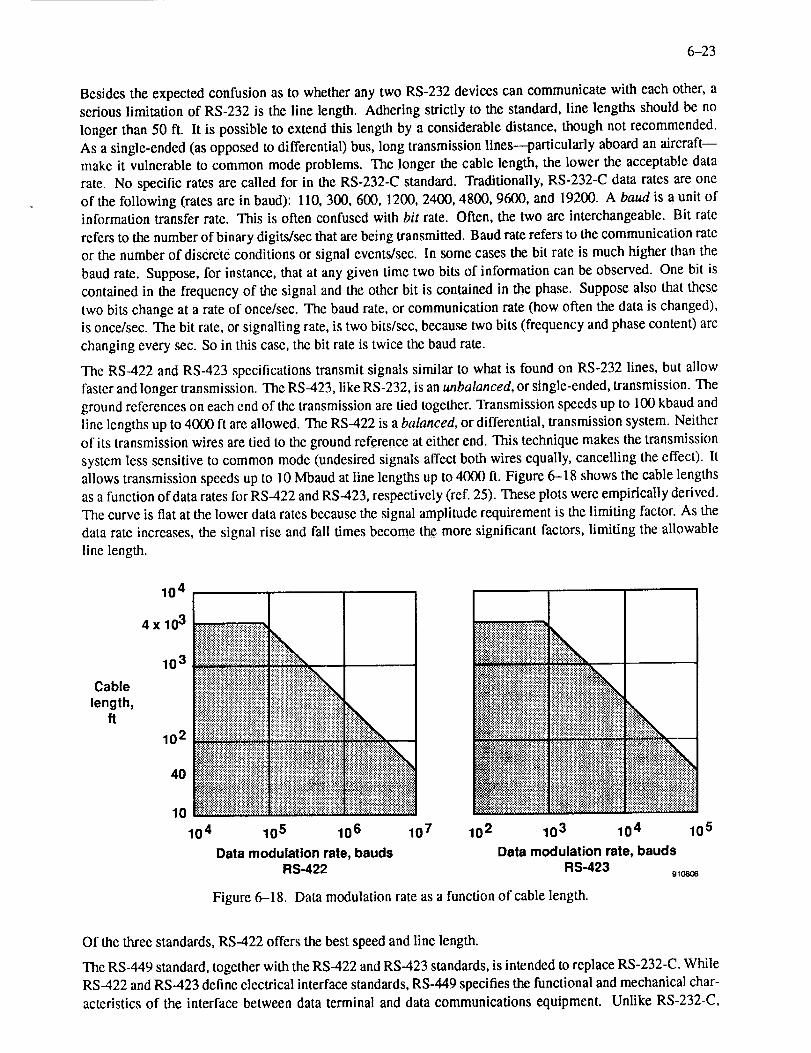
6-23
Besidestheexpectedconfusionasto whetheranytwoRS-232devicescancommunicatewitheachother,aseriouslimitationof RS-232is theline length.Adheringstrictlyto thestandard,line lengthsshouldbenolongerthan50 ft. It is possibleto extendthislengthbyaconsiderabledistance,thoughnotrecommended.As asingle-ended(asopposedtodifferential)bus,longtransmissionlines---particularlyaboardanaircraft--makeit vulnerabletocommonmodeproblems.Thelongerthecablelength,the lowertheacceptabledatarate.Nospecificratesarecalledfor in theRS-232-Cstandard.Traditionally,RS-232-Cdataratesareoneof thefollowing(ratesareinbaud):110,300,600,1200,2400,4800,9600,and19200.A baud is a unit ofinformation transfer rate. This is often confused with bit rate. Often, the two are interchangeable. Bit rate
refers to the number of binary digits/sec that are being transmitted. Baud rate refers to the communication rate
or the number of discrete conditions or signal events/sec. In some cases the bit rate is much higher than the
baud rate. Suppose, for instance, that at any given time two bits of information can be observed. One bit is
contained in the frequency of the signal and the other bit is contained in the phase. Suppose also that these
two bits change at a rate of once/sec. The baud rate, or communication rate (how often the data is changed),
is once/sec. The bit rate, or signalling rate, is two bits/sec, because two bits (frequency and phase content) are
changing every sec. So in this case, the bit rate is twice the baud rate.
The RS-422 and RS-423 specifications transmit signals similar to what is found on RS-232 lines, but allow
faster and longer transmission. The RS-423, like RS-232, is an unbalanced, or single-ended, transmission. The
ground references on each end of the transmission are tied together. Transmission speeds up to 100 kbaud and
line lengths up to 4000 ft are allowed. The RS-422 is a balanced, or differential, transmission system. Neither
of its transmission wires are tied to the ground reference at either end. This technique makes the transmission
system less sensitive to common mode (undesired signals affect both wires equally, cancelling the effect). It
allows transmission speeds up to 10 Mbaud at line lengths up to 4000 ft. Figure 6-18 shows the cable lengths
as a function of data rates for RS-422 and RS-423, respectively (ref. 25). These plots were empirically derived.
The curve is fiat at the lower data rates because the signal amplitude requirement is the limiting factor. As the
data rate increases, the signal rise and fall times become the_more significant factors, limiting the allowable
line length.
10 4
Cablelength,
ft
4x10 3
10 3
10 2
40
10
i:i!:l!i!!=iilliiiiiiiiiiiiii!iiiiiiiiiiiiii!ii iii!!i iii
::.:!:i:i:!:!'!'+';';'!'!::)::;:.:...........
iiliiiliiii!iiiiiiiiiiiiililiiii!!!tiit!i i:::::::::::::::::::::::: _:::
::::::::::::::::::::::::::::::::::::::::::::::::::::::
1114
iiiiiiiiiiii!iii!ili
lii!!iii! lliiliii iiii iiiii
;::: :_: :;; ']::::::::: _:::::::i::::
10 5 10 6
Data modulation rate, baudsRS-422
i !ii !! iii!i iii!i!ii
10 7
/_ ::i_i!iiiiiiiiii::iii_ili/iii_ii_ii_ililiiiill;.> _._......::.._. _........
...... :?:?L-L':. -'L'. - ?.1
:i._::_i.'.'!i!.'.'!!_i$5-'.':_ :'_i_i_iiI ..'.'_.i_i_::_ii_!_!_::_i_ii!Itilittlili iiiiii::::._.%_!::?:_:__:::_::::;:::::::?.;::
•. ,_-_::_ ::_:_::.)::::::::_':::!£,'_ :i_:_.'.':_:_::_:_:_:;:!:!:!;
:. :::::::_..'::._.::::_:.:.:,:::.:f_'_.<>._%!:._._:::,:::::_.....
ilili_iii_iiiiiiiii!_iiiii_;_:::::::::::::::::::::::::::
::::::::::::::::::::::::::::::::::::::::::::::::::::::::::::::::::::
;?.)?i:::?:_!:_:_:::
10 2 10 3
=======================================
10 4 10 5
Data modulation rate, baudsRS-423
9108_6
Figure 6-18. Data modulation rate as a function of cable length.
Of the three standards, RS-422 offers the best speed and line length.
The RS-449 standard, together with the RS-422 and RS-423 standards, is intended to replace RS-232-C. WhileRS-422 and RS-423 define electrical interface standards, RS-449 specifies the functional and mechanical char-
acteristics of the interface between data terminal and data communications equipment. Unlike RS-232-C,
6-24
RS-422,andRS-423,theRS-449standardspecifiesexactmechanicaldefinitions of connectors, which are
37-pin and 9-pin connectors. The RS-449 also clearly states, using diagrams, many of the more poorly under-stood standards stated in RS-232-C. The RS-449 is compatible with CCITT recommendations V.24 and V.54.
In the author's opinion, the only good reason to design flight systems with RS-232 interfaces is to allow easy
interface to existing ground equipment, such as a computer or VDT. Any flight system being used for data
transmission, especially where both ends of the bus can be custom designed, should plan to use a balanced line
standard that allows longer line lengths and higher data rates, such as RS-422.
Despite all attempts to enhance or replace the RS-232-C standard, it is still widely used. Its vagueness allows
designers to believe they have a free hand in bending the standard to their own purposes.
6.6.2 IEEE 488/HP-IB/IEC 625
For better understanding, it is useful to review the history of this bus' development. In the early 1970's, there
was little standardization in connecting measurement test equipment to computer systems. With the advent
of microprocessors, it became feasible to build "smart" instruments that handled major parts of their own
computing tasks. Hewlett-Packard of Cupertino, California, developed a bus to interface measurement instru-
ments like digital voltmeters and scanners to minicomputers. Hewlett-Packard designed many instruments forthis bus named the HP-IB (Hewlett-Packard interface bus) in 1974. Hewlett-Packard participated in various
standardization groups, which used this bus as their starting point in defining industry standards.
In 1976, the International Electrotechnical Commission (IEC) adopted IEC 625-1. It differs from HP-IB
only in the connector used. In 1978, the Institute of Electrical and Electronic Engineers (IEEE) adopted
IEEE 488-1978 (now called 488.1), which is fully complient with HP-IB. The American National Standards
Institute (ANSI) adopted the IEEE Standard and published it as ANSI Standard MC 1.1. The bus concept is
also known as the GP-IB (general-purpose interface bus). Under one or more of these names, the HP-IB has
become widely used throughout the world as a means of making test measurements easier. It is continually
being revised to include enhanced features.
6.6.2.1 Bus operation
The HP-IB operates on two levels: hardware interconnection and message passing. The instrument intercon-
nection is passive. A cable with 16 signal lines (8 for data and 8 for data-message control information) usually
connects the instruments and computer in a daisy-chain fashion. An HP-IB device must function as one of the
following: talker, listener, or controller. A controller device manages the bus, determining which devices are
eligible to send and receive data. A talker can transmit data to other devices on the bus. A listener can receivedata from other devices. Most devices can listen to their control information and then talk to send their mea-
surement results. An HP-IB bus must consist of at least one talker and one listener. Figure 6-19 shows a typical
HP-IB connecti0nl in the figure, one controller (usually a computer) and three instruments, which may be both
listeners (to receive control information) and talkers (to report results back to the controller or other listener)
are shown. The detail illustrates how the daisy chain connections are usually mated by stacking connectors.
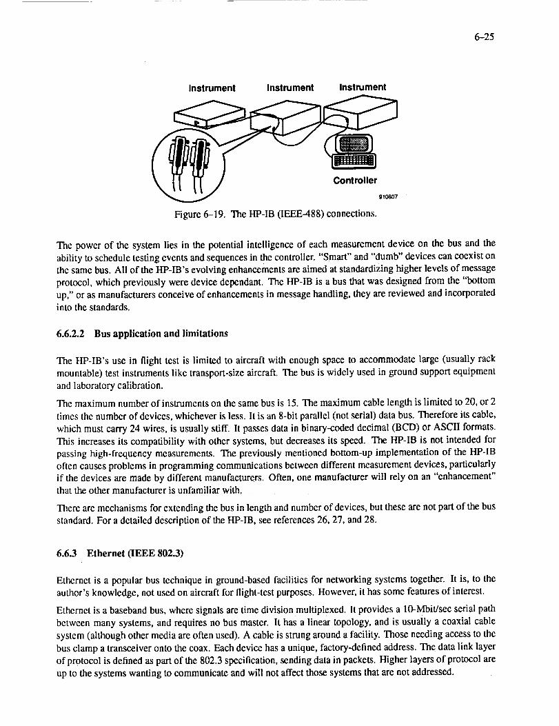
6-25
Instrument Instrument Instrument
Figure 6-19.
Controller
910807
The HP-IB (IEEE-488) connections.
The power of the system lies in the potential intelligence of each measurement device on the bus and the
ability to schedule testing events and sequences in the controller. "Smart" and "dumb" devices can coexist on
the same bus. All of the HP-IB's evolving enhancements are aimed at standardizing higher levels of message
protocol, which previously were device dependant. The HP-IB is a bus that was designed from the "bottom
up," or as manufacturers conceive of enhancements in message handling, they are reviewed and incorporated
into the standards,
6.6.2.2 Bus application and limitations
The HP-IB's use in flight test is limited to aircraft with enough space to accommodate large (usually rack
mountable) test instruments like transport-size aircraft. The bus is widely used in ground support equipment
and laboratory calibration.
The maximum number of instruments on the same bus is 15. The maximum cable length is limited to 20, or 2
times the number of devices, whichever is less. It is an 8-bit parallel (not serial) data bus. Therefore its cable,
which must carry 24 wires, is usually stiff. It passes data in binary-coded decimal (BCD) or ASCII formats.
This increases its compatibility with other systems, but decreases its speed. The HP-IB is not intended for
passing high-frequency measurements. The previously mentioned bottom-up implementation of the HP-IB
often causes problems in programming communications between different measurement devices, particularly
if the devices are made by different manufacturers. Often, one manufacturer will rely on an "enhancement"that the other manufacturer is unfamiliar with.
There are mechanisms for extending the bus in length and number of devices, but these are not part of the bus
standard. For a detailed description of the HP-IB, see references 26, 27, and 28.
6.6.3 Ethernet (IEEE 802.3)
Ethernet is a popular bus technique in ground-based facilities for networking systems together. It is, to the
author's knowledge, not used on aircraft for flight-test purposes. However, it has some features of interest.
Ethernet is a baseband bus, where signals are time division multiplexed. It provides a 10-Mbit/sec serial path
between many systems, and requires no bus master. It has a linear topology, and is usually a coaxial cable
system (although other media are often used). A cable is strung around a facility. Those needing access to the
bus clamp a transceiver onto the coax. Each device has a unique, factory-defined address. The data link layer
of protocol is defined as part of the 802.3 specification, sending data in packets. Higher layers of protocol are
up to the systems wanting to communicate and will not affect those systems that are not addressed.
6-26
Controlof thebusisdeterminedby whogetstherefirst. If anotherdevicewantsto controlthebus,it first
checks for energy on the bus, implying that another system already has control. If it finds that the bus is in use,
it will back off, wait for a random time, and try again. As devices are not allowed to stay on the bus forever,
every device will be guaranteed access.
This bus has become very popular. Many support products, supporting a wide range of physical, data, and
network-link protocol products, exist for several popular computer systems from micros to mainframes.
6.7 Sampling Data Buses for PCM Transmission
In recent years, avionic subsystems involved in navigation, pilot displays, and flight control have become
major parts of aircraft. As these systems must be developed and tested before becoming operational, the
flight-testing community must monitor bus activity between the avionic subsystems. Aircraft data bus activity
must be recorded and, at least in part, be frequently telemetered.
Traditional flight-test data acquisition involves sampling of sensors where the PCM system has control over the
sampling times and sampling rates. With most data buses, however, these transactions take place completely
asynchronous to traditional sampled PCM systems. The engineer must understand what kind of data bus system
information is being sought. Is it important to maintain data bus frame integrity? Must timing relationships
between buses be maintained? Must all bus traffic be recorded or transmitted? Or is it enough to just select
certain bus words and maintain a most-recent-values table for transmission at a noncritical rate? Understanding
the requirements makes a big difference in the complexity of the bus interface scheme used.
In most cases, flight-test engineers want the data acquisition system to monitor the bus, but not interact with it.
Interacting with it infers transmitting some type of data acknowledgment on the bus, which requires the system
under test to take some action on this data or acknowledgment. To some extent, this changes the action of the
system under test. The mark of a good test instrument is one that affects the system under test minimally.
For example, a good voltmeter has a very high impedance, which draws the least current from the system
it is probing.
The following examines the worst case of monitoring data buses--recording all bus activity, including com-
mand words, sync bits, and intermessage gaps, if they exist. Assume that this information must end up in a
digital computer system to evaluate the bus traffic. Two big problems must be addressed: (1) The data bus
speed is probably too high for current flight recorders to handle; and (2) message gaps, if sufficiently long,
introduce a DC component into a signal, and direct (nonmodulated) recording techniques will have trouble.
One common technique for dealing with a high recorder data rate is to split the signal over several tracks, as
was discussed in section 6.5.1.9. For example, bus data can go into a FIFO buffer that splits the stream bit
by bit across five tracks on the tape. Now each track need only record at 1/5 the data rate of the bus. Each
track has a sync word added, and fillers are added during gap times. The tape must be replayed through a
"desplitter" to put the data stream back together.
A good example of sorting out 1553 bus data in real time and storing it in a form amenable to later computer
analysis was developed for Aeritalia in Turin, Italy. Its main goal was to reduce the bandwidth of data recorded
on board so that the number of tracks required on the recorder were also reduced.
This system uses the bus inactive time (usually 40 percent or more) to add timing information and to reduce
the output bit rate. All the information is kept, but in compressed form. Data about the 1553 sync bits, parity,
validity, and so forth are encoded. The time of frame acquisition is also encoded. This allows full analysis of
the bus and maintains time and frame integrity, while not requiring as many filler words in each frame or as
many tracks on the tape. Filler words are required if bus activity is low enough for a period of no transitions
to occur during a PCM frame. The data are stored in a quasi-IRIG format, including sync words and a regular,
cyclic frame pattern. However, the data are not fixed word-position dependent within a frame, like standard
IRIG format. Each frame must be analyzed in software to extract the appropriate information.

6-27
Undernormal bus activity, data can be stored on one tape track. If heavy loading occurs, data can be split
across two tracks. However, it is split on a message-by-message basis, not on a bit-by-bit basis. This is easier
to decommutate and is more reliable. (In the bit-by-bit splitting, if one track dies, all information is lost as they
are so intertwined.) The time tag is optional and is defined as a 16- or 32-bit counter of arbitrary resolution.
Knowledge of 1553 specifications can be used to distinguish between response times, intermessage gap times,
and so forth to check for message validity in the software decommutation. Bus failures can be detected also.
The goal is to reduce the bandwidth of data on board to reduce the tracks required on the recorder. This led
to the pseudo-lRIG technique, because in conventional IRIG PCM, each parameter must have its own slot in
a cyclic frame and would be sent even if it has not changed values. Thus, the bandwidth would be driven
up. A conventional IRIG PCM system would also lose 1553 frame integrity and information about the frame,
sending only data and not "gap" information (ref. 15).
Reference 29 is a good source of information on extracting 1553 bus data from a specially encoded IRIGPCM stream.
6.8 Wave Shaping for Special Situations
6.8.1 Pulse trains for telemetry transmission
Of primary concern in telemetry transmission is bandwidth. That is, how much of the frequency spectrum is
used to transmit a signal. Two factors enter into this: (1) how sharp the rise and fall times of a pulse train are,
and (2) how many transitions/see are required. Minimizing bandwidth requires the pulse train waveshape to
be as nearly sinusoidal as possible, and requires the bit rate to be minimized.
The simplest coding technique also corresponds to the lowest bandwidth signal: NRZ-L (nonreturn to zero-
level). Its power spectral density centers around the bit rate. In this code, a logic 1 is a high and a logic 0
is a low. Unfortunately, no transitions take place when a long string of O's or l's occur. Sophisticated bit
synchronizers must be used to keep the data stream in lock.
6.8.2 Pulse trains for tape recording
Tape recorders are sensitive to steady-state response. This means that long periods of no transition in a data
stream do not record well. Therefore, NRZ-L coding is not usually the coding of choice. A code that requires
transitions to occur at least every bit time or two works better. Codes like BI_-L (Manchester II biphase-
level) and DM-M (delay modulation-mark (Miller)) are commonly used. Pseudorandom techniques that shift
the power spectral density curve closer to the bit rate while keeping it off of steady-state condition are better.
Figures 94 and 97 of reference 1 show code definitions and power spectral density curves, respectively.
6.8.2.1 Filtering and encoding considerations
For tape recording of digital PCM streams, one of the most important considerations in direct recording is the
power spectral density of the signal. The coding technique selected depends on this. For example, an NRZ-L
signal does not guarantee that there will be any transitions in a given length of time from 0 to 1 or from 1 to
0. If the data being recorded are all O's or all l's, there are no transitions and no self-clocking is possible. All
information is DC, which is not suitable for tape recording. The BI_-L code has zero-frequency components
at DC. However, its bandwidth is approximately twice that of NRZ-L. The DM-M code has a small amount
of frequency components at DC with approximately the same bandwidth as NRZ-L, which makes it a good
compromise for tape recording. This subject is covered in more detail in reference 1.
6-28
6.8.2.2 Enhancement techniques
Sometimes recording high-speed data streams is complicated by not having recording mechanisms that can
keep up. In other words, linear recording of data streams cannot always be done. One technique that has
been used to work around this bandwidth limitation is called track splitting, which is discussed in detail in
section 6.7. In track splitting, serial data stream is sliced up and consecutive chunks are laid in parallel tracks of
a recorder. This complicates the encoding onto the recorder as well as decoding it later. It does, however, allow
more recording time on a given tape. The technique has been used successfully in recording MIL-STD-1553
avionics data (at one Mbit/sec) onto 14-track tape recording at a much slower rate.
An important enhancement technique that is sometimes overlooked is to reduce the amount of data recorded.
In many situations, not all of the bus traffic is required for analysis. Careful selection of parameters can
significantly reduce recording requirements.
7-1
7 DIGITAL DATA STORAGE
7.1 Tape Recorders
Tape recorders have been the mainstay of flight data acquisition systems for many years. Though ground-based
computer systems also have used tape recording for many years, their mechanism of storage differs from most
flight systems. Ground-based systems typically store information in parallel across several tracks in a "byte
serial" fashion. This can be thought of as digital recording. Hight systems, in contrast, usually record in an
analog fashion. Even if data is digitized before being sent to the recorder, it is recorded in a "bit serial" fashion,one track/channel or data stream.
Flight recorders have several tracks; 14 or 28 are common. Each track can record one PCM data stream or one
FM channel. So for a 14-track tape unit, up to 14 FM channels or 14 PCM data streams can be recorded, or
a mixture of the two. One track is usually devoted to recording the IRIG time to synchronize data acquisition
with the actual time the data was taken.
This kind of tape recording has limited bandwidth--I to 2 hr recording at data rates under 300 kbit/sec. Tech-
niques have been developed to use track splitting: spreading a serial data stream across several tracks. This
technique is commonly used for storing high-speed data streams in real time. References 1 and 15 provide
information about tape recording, signal conditioning, and encoding.
7.2 Semiconductor Memory
Semiconductor memory has been among the most exciting technologies to watch over the past several years.
Memory densities have increased dramatically, while costs and power consumption have plummeted. Fifteen
years ago, minicomputer systems containing more than 32 kbytes of memory were uncommon. Today, many
laptop computers contain 1 or 2 Mbytes.
7.2.1 Random access memory
Memory capacity, speed, weight, size, and power consumption are key issues in selecting memory for data
storage. Cost is usually less of an issue. Random access memory (RAM) is a type of read-write memory; that
is, each memory location can be accessed in any random order and each location can be either read from or
written to. For data storage requiring high speed, it is hard to exceed the performance of RAM. Much of the
information stored passes through RAM anyway in the process of passing it on to the storage device. Densities
reach a level where size and weight are acceptable for low to medium amounts of data storage in flight test.
For example, if a flight test project has 20 parameters, each requiring 200 samples/sec for a testing period of
30 min, then this would require 7.2 x 106 bytes of storage:
200 samples/sec for each of 20 parameters (one parameter/byte)
(200 frames/sec)(20 parameters/frame) = 4000 parameters/sec
(4000 parameters/sec)(30 min)(60 sec/min) = 7.2 x 10⁶ parameters
This is a modest requirement for flight testing, but a fairly sizable one for the amount of RAM required. Data
storage using RAM tends to be for infrequent, or noncontinuous, storage of data (like test points that span a
few seconds).
The RAM is volatile. It requires the application of power at all times to retain its contents. Sophistication
in integrated circuit design has allowed modern IC's to automatically revert to a standby mode when its data
is not externally required. Standby mode requires considerably less power, usually a few/zamps/IC. Small
batteries can keep their contents intact for several months or years.
7-2
7.2.2 Electrically erasable programmable read only memory
The EEPROM (or E2 PROM) is a nonvolatile memory device (requiring no battery backup power) that can
be programmed or reprogrammed (erased) electrically while still in its application circuit (ref. 8). It is well
suited for systems requiring small amounts of data storage updated infrequently with noncritical write times
(in the msec range). Calibration tables are a good example. The tables may be updated without removing the
EEPROM and are not expected to change during a flight. The table values can be expected to be retained even
after circuit power has been removed.
73 Bubble Memory
Bubble memory uses a method of storing information in tiny magnetic domains, called bubbles. Access to
the bubbles is sequential--in rotating order. The bubbles store information in a nonvolatile manner, and in-
formation is not lost when power is removed. This storage is completely solid state, and therefore holds much
promise in environments like flight test, where lack of vibration-sensitive mechanical parts is desirable.
Bubble memories became available commercially in the early 1980's, but were never widely used. In its early
days, these memories were the subject of much advertising "hype" (promises that were never lived up to). Its
low-memory densities, low-speed, heavy-weight, complex support circuitry, lack of substantial improvements,
and high cost have conspired to keep bubble memories out of most applications.
Bubble memories have been used in flight testing applications, but only those where infrequent access of "read-
mostly" memory was required, and access times were not time critical. One such application was instrumented
by the NASA Ames Research Center's Dryden Flight Research Facility to support a laminar (smooth air) flow
research program onboard a Lockheed C-140 Jetstar aircraft. That system used bubble memory cards in two of
the onboard systems. The bubble memory was designed commercially to emulate standard Q-bus floppy disks.
They were accessed only to assist the system when powered up and to load the application program into semi-
conductor (volatile) memory for execution. In this application, real-time response was unnecessary; vibration
resistance and small physical size (relative to the floppy disk drive it replaced) were positive attributes.
7.4 Disks
7.4.1 Magnetic (hard and flexible)
Magnetic disks are a very popular way of saving flight data. They are widely used in ground-based systems
and are increasingly used on aircraft.
These disks are excellent media to store and retrieve random access data. Access times range in the tens to
hundreds of msec, and data capacities are between a few hundred kilobytes and a few hundred megabytes.
Flexible (floppy) disks are at the low end of the range in terms of speed and capacity, and hard disks are at the
high end.
An advantage of flexible disks is low media cost and high portability. They are also "contact head" devices
and are thus less sensitive to vibration problems than are hard disks. Their data transfer rates are in the range
of 250 to 500 kbit/sec.
The advantages of hard disks are speed and high-storage capacity. Data transfer rates are from 5 to 10 Mbit/sec.
Many hard disks are also sealed (Winchester type) and are less susceptible to a dusty environment than are
flexible disks. However, hard disks use expensive media and are "floating head" devices; that is, their recordingheads must not contact the surface of the disk. This event is called a head crash and results in the loss of data
(and usually a service call to repair the head). Vibration could result in head crashes, and considerable attention
must be paid to mounting the drives to prevent this kind of damage, particularly in flight testing.
7-3
7.4.2 Optical
Optical disk data storage is emerging as a very exciting technology for data storage. There are few standards
currently, as it is still in its infancy. The most important advantage of optical media is its extremely large
storage capacity. Storage capacities in the Gbyte range are not uncommon. The most mature technology is the
so-called write once, read many (WORM) optical disks. As the name implies, data can be written to the media
only once, but read back many times. This is ideal for archiving data like flight data. It is better protected from
accidental erasure than is magnetic media. It also tends to be optimal for sequentially stored data because it
is recorded in a continuous spiral, like the groove on a record player. Currently, WORM recording speeds are
not tremendously fast, averaging a few Mbit/sec.
7.4.3 Interfacing
There are several standards available to interface to rotating disk drives. Interfaces are usually addressed at two
levels: drive to controller and controller to processor. The ST506 specification and ESDI define the signals
passing between the drive and its controller. The MSCP defines the protocol required for the controlling
processor to communicate with the controller attached to the drive(s). The SCSI is a combination of both
(protocol and bus). Thus, a drive interface may use both ST506 and MSCP, or just SCSI. Sometimes converters
are used to allow a processor sending commands on a SCSI bus to communicate with a drive using ST506.
The SCSI is used for more than just disk drives. It is also a general-purpose data transfer bus. With a properly
designed system, the processor does not need to know physical details about the device it is communicating
with. Whether the device is a disk drive, magnetic tapeddve, or a printer, there is little impact on the commands
sent from the processor.

8-1
8 TESTING
8.1 Failure Modes and Mechanisms of Digital Systems
Modern electronic systems are, for the most part, very reliable systems. Comprised largely of solid-state
devices, they are fairly impervious to shock. Their low power consumption minimizes heat damage, and shelf
life is virtually unlimited. However, statistically, the more components added to a system, the more likely
something will fail. The trend toward highly complex aircraft systems therefore works against the addition of
more reliable components.
Digital systems, by nature, tend to be much more impervious to temperature variations than their analog coun-
terparts (see sec. 1.2). Even the analog circuits, while sensitive to temperature variations, are usually not
subject to catastrophic failure---except for components that, by the nature of their operation, are expected to
dissipate much heat.
However, digital logic is more sensitive to power fluctuations than is analog circuitry. For example, if a current
surge (resulting from the sudden switching of a logic level) causes a spike on the power supply line, the logic
thresholds of a logic chip may be affected. This, in turn, may cause a logic chip to misinterpret a logic level. As
logic circuits make substantial use of memory elements (future action depends on the past), the misinterpreting
of a logic level can cause the logic to take a wrong "fork in the road" and get very confused. In contrast, most
analog circuits have no memory element, so a temporary perturbation in power has no lasting impact on the
system's performance.
After eliminating (relatively speaking) catastrophic failure and power fluctuations, the failure modes in digital
systems are primarily those of synchronization. Assuming that a system has been functional and suddenly
develops problems, a good area to look at is the timing relationships between various parts of the system. This
is where most time is spent troubleshooting digital systems.
8.2 Hardware Test Methods
In the process of designing and testing digital electronics, like any other electronic system, it is necessary to
find and fix problems as well as to evaluate performance. In traditional analog electronic testing, the most
important general-purpose test gear is the oscilloscope. In testing digital electronics, the logic analyzer is a
very important piece of test gear. This device is a specialized data acquisition tool that allows the operator to
see the timing relationships between several digital signal lines. Timing is everything in digital systems. The
logic analyzer lets the evaluator see the timing relationships between the various digital signals in the system.
Glitch detectors can spot signals that appear and disappear between samples--which may point to "illegal"
activity on a channel.
Digital oscilloscopes are gaining in popularity. They combine the principles of both logic analyzers (by sam-
pling data digitally) and the analog oscilloscope (by displaying voltage level). Sometimes logic analyzers
include one or two channels of digital oscilloscope channels that allow the synchronized observation of the
digital timing with observed analog traces.
Pattern generators and microprocessor emulators control the logic (provide a forcing function). Microprocessor
emulators are used in development when not all of the hardware is built, or when the system is built and
interaction with the "guts" of the system is required for testing. A typical emulator will plug into the system in
place of a microprocessor and will allow the user to map recognized memory into either the system under test
or the emulator itself. In designing embedded microprocessor systems, an emulator is almost indispensible.
An understanding of the timing relationships in a working system is important to check for anomalous opera-
tion. Good baseline measurements should be made when the system is declared operational. This is similar to
taking your temperature when you are well so that you know what is normal.
8-2
If it is possibleto usesocketsfor components,thejob of troubleshootingasystematthecomponentlevelis greatlysimplified.Simplyreplacesuspectedcomponentsuntil thesystemworks,or replaceall partsandreinsertsuspectcomponentsuntil it fails. However,useof socketsgreatlyincreasesthepossibilityof abadconnection,whichobviouslyinducesfailuremodes.
Muchof aircraftavionictestingthatconcernsaflighttestor instrumentationengineerinvolvesmakingblackboxescommunicateproperly.This frequentlyrequiresspecializedtestingequipmentthatis ableto analyzedatabustrafficandinterpretitsmessages.Theseunitsareoftenexpensive,butcansaveanenormousamountof timein focusingonaproblem.
8.3 Software Test Methods
Software is found in many electronic devices today. Hard-wired logic circuits are giving way to firmware
(programmed hardware)-controlled logic. More high-level control of sequences (especially those requiring
decisions based on parameters that change) use more conventional software. As technology makes it possible
to include more processing capability and memory capacity into less space and power, imbedded software is
found in more subsystems.
Testing software systems can be challenging. Communication between several processors controlled by several
(unsynchronized) oscillators guarantees that the system cannot be tested under all possible conditions. The
author has seen digital systems work successfully for several years before a particular set of conditions occurred
(as a result of synchronization problems) that caused erroneous operation.
The best a designer can do is to pay attention to timing delays, signal degradation over transmission lines, and
design error detection and correction, as well as synchronizing (acknowledge) mechanisms, where possible.
The more a system is modularized, that is, its components act independently without depending on much
interplay between subsystems, the easier it is to test. Program logic can then be tested on a subsystem-by-
subsystem basis using well-understood tools like program debuggers and emulators (secs. 2.5.2 and 8.2). It
is like the difference between being accountable for your own actions as opposed to being responsible for the
detailed actions of other people. There is only so much control you can exercise over someone else. As aircraft
systems become more complex, modularity becomes the key to successfully testing and integrating systems.
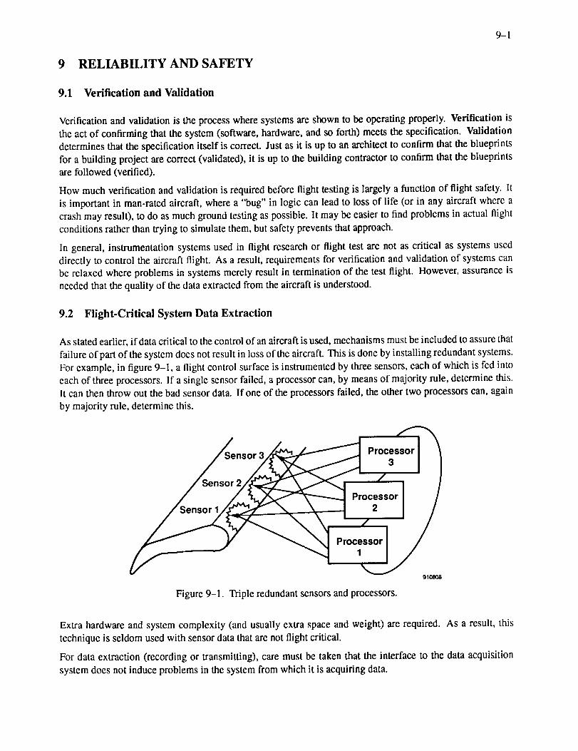
9-1
9 RELIABILITY AND SAFETY
9.1 Verification and Validation
Verification and validation is the process where systems are shown to be operating properly. Verification is
the act of confirming that the system (software, hardware, and so forth) meets the specification. Validation
determines that the specification itself is correct. Just as it is up to an architect to confirm that the blueprints
for a building project are correct (validated), it is up to the building contractor to confirm that the blueprints
are followed (verified).
How much verification and validation is required before flight testing is largely a function of flight safety. It
is important in man-rated aircraft, where a "bug" in logic can lead to loss of life (or in any aircraft where a
crash may result), to do as much ground testing as possible. It may be easier to find problems in actual flight
conditions rather than trying to simulate them, but safety prevents that approach.
In general, instrumentation systems used in flight research or flight test are not as critical as systems used
directly to control the aircraft flight. As a result, requirements for verification and validation of systems can
be relaxed where problems in systems merely result in termination of the test flight. However, assurance is
needed that the quality of the data extracted from the aircraft is understood.
9.2 Flight-Critical System Data Extraction
As stated earlier, if data critical to the control of an aircraft is used, mechanisms must be included to assure that
failure of part of the system does not result in loss of the aircraft. This is done by installing redundant systems.
For example, in figure 9-1, a flight control surface is instrumented by three sensors, each of which is fed into
each of three processors. If a single sensor failed, a processor can, by means of majority rule, determine this.
It can then throw out the bad sensor data. If one of the processors failed, the other two processors can, again
by majority rule, determine this.
enso_
91O8O8
Figure 9-1. Triple redundant sensors and processors.
Extra hardware and system complexity (and usually extra space and weight) are required. As a result, this
technique is seldom used with sensor data that are not flight critical.
For data extraction (recording or transmitting), care must be taken that the interface to the data acquisition
system does not induce problems in the system from which it is acquiring data.

R-1
REFERENCES
Veatch, Donald W., and Rodney K. Bogue, Analog Signal Conditioning for Flight-Test Instrumentation,°
AGARDograph no. 160, vol. 17, 1986. Also published as NASA RP-1159, 1986.
2. Spitzer, Cary R., Digital Avionics Systems, Prentice-Hall, Englewood Cliffs, N J, 1987.
3. The TTL Data Book for Design Engineers, Texas Instruments, Inc., Dallas, TX, 1973.
4. CMOS Logic Databook, National Semiconductor, Santa Clara, CA, 1988.
5. ALS/AS Logic Data Book, Texas Instruments, Inc., Dallas, TX, 1988.
6. FASTData Manual, Signetics, Sunnyvale, CA, 1986.
7. FACT TM Advanced CMOS Logic Databook, reprint of Fairchild 1987 FACT Databook, National
Semiconductor, Santa Clara, CA, 1987.
8. Prickett, M.J., Microprocessor Applications in Airborne Flight Test Instrumentation, AGARDograph no.
160, vol. 18, 1987.
9. Meiksin, Z.H., and Philip C. Thackray, Electronic Design with Off-the-Shelflntegrated Circuits, 2d ed.,
Prentice-Hall, Englewood Cliffs, NJ, 1984.
10. DSPatch, nos. 14, 15, & 16, Analog Devices, Inc., Norwood, MA, Summer 1990.
11. Wilner, Douglass O., and Glenn A. Bever, An Automated Stall-Speed Warning System, NASA TM-84917,
1984.
12. Data Conversion Products Databook, Analog Devices, Inc., Norwood, MA, 1988.
13. Rabiner-Bernard Gold, Lawrence R., Theory and Application of Digital Signal Processing, Prentice-Hall,
Englewood Cliffs, NJ, 1975.
14. Oppenheim, Alan V., and Ronald W. Schafer, Digital Signal Processing, Prentice-Hall, Englewood Cliffs,
NJ, 1975.
15. Goodenough, Frank, "Switched-Capacitor Filters," Electronic Design, vol. 37, no. 8, Apr. 13, 1989,
pp. 77-92.
16. Cattunar, S., "Acquisition and Recording an AMX AJC Aeritalia Experience and Present Trends," pre-
sented at the European Telemetry Conference, Aix-en-provence, France, June 1987.
17. Dornhoff, Larry, Notes on Applied Modern Algebra, Stipes Publishing Co., Champaign, IL, 1975.
18. MIL-STD- 1553B, Aircraft Internal Time Division Command�Response Multiplex Data Bus, Military Stan-
dard, U.S. Department of Defense, Sep. 21, 1978.
19. MIL-STD- 1553, Multiplex Applications Handbook, Military Standard, U.S. Air Force Systems Command,
1982. Available from SCI Systems, Inc., Huntsville, AL.
20. Mark 33 Digital Information Transfer System (DITS), ARINC Specification 429-9, Aeronautical Radio,
Inc., Annapolis, MD, 1985.
21. Harris Corp. Data Sheet for HS-3282, Harris Corp., Palm Bay, FL, 1985.
22. "Interface Between Data Terminal Equipment and Data Communication Equipment Employing Serial
Binary Data Interchange," EIA RS-232-C, Electronic Industries Assoc., Wash., DC, Aug. 1969.
23. "Character Structure and Character Parity Sense for Serial-by-Bit Data Communication in the American
National Standard Code for Information Exchange," ANSI X3.16-1976, American National Standards
Institute, New York, 1976.
24. Recommendation V3, International Alphabet No. 5, CCITI', vol. VIII. 1, Geneva, Switzerland, 1977.
R-2
29.
25. McNamara,JohnE.,Technical Aspects of Data Communication, Digital Equipment Corp., Bedford, MA,
1978.
26. Digital Interface for Programmable Instrumentation, ANSI/IEEE 488.1-1987, Institute of Electrical and
Electronics Engineers, New York, June 1987.
27. ANSI�Codes, Formats, Protocols, and Common Commands, ANSI/IEEE488.2-1987, Institute of Electri-
cal and Electronics Engineers, New York, Apr. 1987.
28. IEC 625-I, An Interface System for Programmable Measuring Instruments (Byte Serial, Bit Parallel).
Part I: Functional Specifications, Electrical Specifications, Mechanical Specifications, System Applica-
tions and Requirements for the Designer and User, International Electrotechnical Commission, Geneva,
Switzerland, 1979.
Vitalone, G., "Decommutation Techniques and Their Integration Into Post Flight Analysis System," pre-
sented at the European Telemetry Conference, Aix-en-Provence, France, June 1987.
Index
A
A-D 0-1, 3-1, 3-2, 3-3, 3-4, 3-8, 3-10, 3-11,3-12
ADA 2-7, 2-8Aeritalia 6-26
aliasing 1-3, 3-5, 3-8, 5-4
amplifier 3-1
analog 0-1, 1-1, 1-2, 1-3, 2-1, 3-1, 3-2, 3-3,
3-4, 3-5, 3-7, 3-8, 5-1, 5-2, 5-3, 5-4,
6-14, 7-1, 8-1
to digital, 0-1, 3-1, 3-2, 3-3, 3--4, 3-5, 3-7,
3-8, 3-10, 3-11, 3-12
ARINC 0-1, 6-3, 6-14
419,6-14,6-15
429, 6-3, 6-15
575, 6-16
629, 6-19
704, 6-16
ASCII 0-1, 6-22, 6-25
asynchronous 2-7, 6-2, 6-9, 6-11, 6-16, 6-19,
6-20, 6-21, 6-22, 6-26
avionics 0-1, 1-1, 2-1,2-7, 6-6, 6-13, 6-14, 6-
17, 6-18
B
bandwidth 1-3, 3-8, 5-4, 6-2, 6-3, 6-4, 6-5, 6-6,
6-13, 6-14, 6-26, 6--27, 6-28, 7-1
Bocing 6-19, 6-20
737, 6-19
bubble memory 7-2
C
"C" language 2-7
calibration 3-6, 3-11,4-2, 6-25, 7-2
code
Gray, 4-3
nonprogressive, 4-1, 4-3
progressive, 4-2
communication 6-1, 6-23, 8-2
parallel, 6-3, 6-6, 6-25, 6-28, 7-1
serial, 1-2, 2-1,2-7, 6-3, 6-4, 6-6, 6-7, 6-15,
6-16, 6-21,6-22, 6-25, 6-28
computer 0-1, 2-2, 2-8, 3-5, 3-7, 4-2, 4-3, 6-2,
6-3, 6-4, 6-6, 6-14, 6-21, 6-24, 6-26,
7-1
cost 2-2, 2-6, 2-8, 3-2, 6-6, 6-7, 7-1, 7-2
D
D-A
data0-2, 3-3, 3-5, 3-6
I-1
acquisition, 0-1, 1-2, 2-1,2-6, 2-7, 3-8, 5-1,
5-4, 6-5, 6-20, 6-26, 7-1,9-1
compression, 5-4
rate, 1-3, 6-1, 6-2, 6-3, 6-13, 6-16, 6-18,
6-23, 6-26, 7-1
storage, 7-1, 7-2, 7-3stream, 1-2, 2-6, 6-2, 6-3, 6-10, 6-12, 6-13,
6-18, 6-26, 6-27, 6-28, 7-1
data bus
1553, 6-3, 6-6, 6-14, 6-16, 6-18, 6-20, 6-26,
6-27, 6-28
1773, 6-6, 6-14
ARINC, 6-14
ethernet, 6-25
H009, 6-20
HP-IB, 6-24
RS-232, 6-21, 6-23, 6-24DATAC 6-19
development
hardware, 8-I
software, 2-8
digital
filter, 3-4, 5-1, 5-2, 5-4
sensors, 2-1,4-1, 4-2
to analog, 0-2, 3-3, 3-4, 3-5, 3-6
to synchro, 3-6, 3-7transducer, 4-1,4-2
disk
coded, 4-1
floppy, 7-2
hard, 7-2
optical, 7-3
displays 2-1, 3-7, 6-7, 6-19, 6-20, 6-21, 6-26
E
ECC 0-2, 6-5
EEPROM 0-2, 7-2
EMI 0-2, 6-2
emulator 8-1
EPLD 0-2, 2-5
error
detection, 6-4, 8-2
sources, 3-4, 3-7, 3-10, 5-4, 6-6
ESD 0-2, 2-6
ethernet 6-25
F
failure 2-6, 6-13, 6-27, 8-1, 9-1
fiber optics 6-1, 6-3, 6-14
FIFO 0-2, 6-14, 6-26
I-2
1553 6-3, 6-6, 6-14,6-16,6-18,6-20,6-26,6-27,6-28
filterantialias,1-3,3-8,5-4digital,3--4,5-1,5-2,5-4FIR,5-1IIR,5-1presample,3-8,3-10,5-1statistical,5-4switchedcapacitor,5-2transmission,6-27
FIR 0-2,5-1flightcontrol 0-1, 1-1,2-1,3-5,6-2,6-7,6-17,
6-19,6-20,9-IFM 0-2, 1-3,5-4,6-13,7-1FORTRAN2-7
Ggain 3-6,3-7,5-1glitch 4-1,4-3,8-1Graycode 4-3
Hhelicopter6-3HP-IB 0-3,6-24hybridcircuits 2-6, 6-18
IIIR 0-3, 5-1
IRIG 0-3, 6-2, 6-4, 6-14, 6-26, 7-1isochronous 6-3
L
language 2-7, 2-8
logic
analyzer, 8-1
logic families, 2-2, 2-3, 2-5, 2-6
M
Manchester code 0--2, 6-10, 6-27
memory 7-1, 7-2
N
NASA 0-1,0-3, 6-2, 6-19, 7-2
navigation 2-1, 6-6, 6-16, 6-17, 6-19, 6-20,6-26
Nyquist rate 3-4, 3-9, 3-10, 5-3, 5-4
O
optical 1-1, 6-1
disk, 7-3
encoder, 4-1
fiber, 6-1, 6-3, 6-6, 6-14
P
PASCAL 2-7
PCM 0-3, 6-2, 6--4, 6-14, 6-19, 6-26, 6-27
performance 1-1, 2-6, 5-1, 6-18, 7-1, 8-1
R
RAM 0-3, 7-1
redundancy 3-9, 6-2, 6-7, 6-13, 6-17, 9-1
reliability 2-2, 3-6, 6-7, 6-27, 8-1,9-1
resolution 1-3, 3-1, 3-2, 3-3, 3-4, 3-5, 3-8,
3-11, 3-12, 5-3, 6-16, 6-27
RF 0-3, 6-2, 6-3
RS-232 6-21, 6-23,6-24
RS-422 6-23, 6-24
RS-423 6-23
RS-449 6-23
S
sampling rates 1-3, 3-1, 3-4, 3-5, 3-8, 3-9, 6-2,6-18, 6-26, 7-1
signal conditioning 1-1, 2-1,7-1simulation 2-8
sync bits 6-11, 6-26
synchro to digital 3-7
synchronize 2-7, 4-3, 6-3, 6-13, 6-27, 7-1, 8-1,8-2
synchronous 4-1, 6-2, 6-3, 6-6, 6-19
T
tape 1-2, 5-4, 6-10, 6-13, 6-14, 6-26, 6-27,6-28, 7-1
telemetry 1-1, 2-1, 6-1, 6-2, 6-3, 6-4, 6-27
temperature 1-1, 2--6, 3-2, 3-10, 5-1, 8-1
test equipment 6-24, 6-26, 8-1, 8-2
track splitting 6-13, 6-26, 6-27, 6-28, 7-1
V
vibration 5-1, 5-4, 7-2
video 6-13, 6-21
W
weight 6-1, 6-2, 6-3, 6-4, 7-1, 7-2, 9-1wire 2-7, 6-1, 6-3, 6-4, 6-15, 6-19, 6-23, 6-25
N/ A Report Documentation PageNa|o_d A_om'_euEe$ mM
_mol Adm_lW_on
1. Report No.
NASA TM-101739
4. Title and Subtitle
2. Govemrnent Accession No.
Digital Signal Conditioning for Flight Test Instrumentation
7. Author(s)
Glenn A. Bever
9. Performing Organization Name and Address
NASA Ames Research Center
Dryden Flight Research Facility
P.O. Box 273, Edwards, California 93523-0273
12. Sponsoring Agency Name and Address
National Aeronautics and Space Administration
Washington, DC 20546-3191
3. Recipient's Catalog No.
5. Report Date
March 1991
6. Performing Organization Code
8. Performing Organization Report No.
H- 1695
10. Work Unit No.
RTOP 533-02-51
11. Contract or Grant No.
13. Type of Report and Peried Covered
Technical Memorandum
14. Sponsoring Agency Code
15. Supplementary Notes
Prepared for and sponsored by the AGARD Flight Mechanics Panel, Flight Test Techniques Working
Group, as part of AGARDograph 160, Flight Test Instrumentation Series.
16. Abstract
This volume in the AGARD Flight Instrumentation Series provides flight test insu'umentation
engineers with an introduction to digital measurement processes on aircraft. Flight test instrumentation
systems are rapidly evolving from analog-intensive to digital-intensive systems, including the use of
onboard digital computers. Topics include measurements that are digital in origin, as well as sampling,
encoding, transmitting, and storing of data. Particular emphasis is placed on modern avionic data bus
architectures and what to be aware of when extracting data from them. Examples of data extraction
techniques are given. Tradeoffs between digital logic families, trends in digital development, and design
testing techniques are discussed. An introduction to digital filtering is also covered.
17. Key Words (Suggested by Author(s))
Data acquisition; flight test instrumentation;
flight test measurement; signal conditioning; and
digital data buses
19. Security Classif. (of this report) 20. Security Classif. (of this page)
Unclassified Unclassified
18. Distribution Statement
Unclassified - Unlimited
Subject category 06
21. No. of Pages 22. Price
81 A05
NASA FORM 1626 OCT86 For sale by the National Technical Information Service, Springfield, Virginia 22161-2171