drift diffusion hw
TRANSCRIPT
8/12/2019 Drift Diffusion Hw
http://slidepdf.com/reader/full/drift-diffusion-hw 1/3
Introduction to Semiconductor Devices
(Purdue University EE 305/606)
Supplemental Homeor! E"ercises
Tutorial questions based on Drift-Diffusion Lab v1.0 available online at
http://www.nanohub.org.
Reference book: Semiconductor Device Fundamentals b Robert !. "ierret #$hapter %&
Concept : Drift
'(& )et us consider an intrinsic Si slab of length *.(um at room temperature #T+%** ,&.
#Select !-periment ( for this question&
#a& Dope the semiconductor to a+ (e(0 /cm% and ramp voltage from * to 12. $ommenton the 342 characteristics.
#b& ow dope the semiconductor to d+ (e(0 /cm% and ramp voltage from * to 12.
$omment on the 342 characteristics.
#c& 5enerate vd #cm/sec& vs ! #2/cm& curves for holes and electron from #a& and #b&. 6hatis the saturation velocit7
#d& !-tract electron #8n& and hole #8 p& mobilit values from the figure generated above.
'1& ow9 let us consider an Si slab of length *. um. #Select !-periment ( for thisquestion&
#a& ;t room temperature9 dope it 4tpe #d& in steps from (e(0/cm% to (e(</cm%.
$alculate electron mobilit #8n& for each doping level.
#b& Similarl dope the semiconductor "4tpe #a& in steps from (e(0/cm% to (e(</cm%.$alculate hole mobilit #8 p& for each doping level.
#c& "lot 8n vs d and 8 p vs a. 6h do mobilit values reduce at high doping levels 7#d& For each doping level in #a& var temperature #T& from 1** , to **,.#e& For each doping level in #b& var temperature #T& from 1**, to **,.
#f& "lot 8n vs T and 8 p vs T at different doping levels. 6h does mobilit increase with
decreasing temperature7
Concept: Diffusion
'%& $onsider a Si slab of length 0 um at room temperature. )et light shine on the leftedge with a penetration depth of *.( um. The e4h pair generation rate due to light shining
be9 5+ (e1% /cm%.s. 3n realit the minorit carrier life times are in the order of few
hundreds of micro4seconds. Diffusion length #) p& calculated using L p= D p× p 9 where D p and = p are diffusion coefficient and minorit carrier life time.
#a& $alculate the diffusion length for a(. n4 tpe semiconductor slab with = p + (* μs. 6hat is the hole diffusion coefficient
provided bulk silicon hole mobilit is 0* cm1 24(s4( at %**,.1. p4 tpe semiconductor slab with =n + (* μs. 6hat is the electron diffusion
coefficient provided bulk silicon electron mobilit is (0** cm1 24(s4( at %**,.
>ow does this length compare with the actual device lengths 7
8/12/2019 Drift Diffusion Hw
http://slidepdf.com/reader/full/drift-diffusion-hw 2/3
#b& To understand the phenomena of diffusion we can choose a ratio for D p / ) p where
D p is the diffusion coefficient and ) p is the minorit diffusion length. This ratio for device
simulation must be kept small which is governed b the minorit carrier life time
according to this formula : L p
p
=
D p
L p
?sing the calculated diffusion coefficients from part #a&9 what value for minorit carrier
life time must be set to obtain a diffusion length of around (μm 7
ow set =n +(ns and = p +(ns #for simulation purpose& and do the following simulations.
#c& 3f the semiconductor is doped 4tpe d+(e( /cm%. Do low level in@ectionconditions prevail inside the illuminated bar. !-plain7
#d& Sketch e-cess minorit carrier concentration and compare with simulated result.$alculate hole diffusion coefficient9 D p from this result.
#e& Suppose the semiconductor was "4tpe a+(e( /cm%. Do low level in@ectionconditions prevail inside the illuminated bar7
#f& Sketch e-cess minorit carrier concentration and compare with simulated result.$alculate electron diffusion coefficient9 Dn from this result.
>ow do the values of diffusion coefficient calculated compare with the values from part
#a&.
Concept: Quasi-Fermi Level
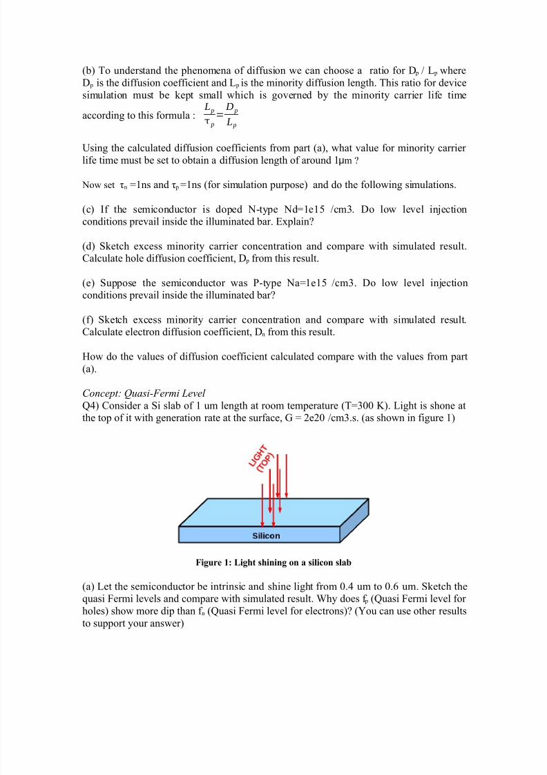
'0& $onsider a Si slab of ( um length at room temperature #T+%** ,&. )ight is shone atthe top of it with generation rate at the surface9 5 + 1e1* /cm%.s. #as shown in figure (&
#i$ure %& 'i$t sinin$ on a silicon sla
#a& )et the semiconductor be intrinsic and shine light from *.0 um to *.A um. Sketch thequasi Fermi levels and compare with simulated result. 6h does f p #'uasi Fermi level for
holes& show more dip than f n #'uasi Fermi level for electrons&7 #Bou can use other results
to support our answer&

8/12/2019 Drift Diffusion Hw
http://slidepdf.com/reader/full/drift-diffusion-hw 3/3