dual wideband high output current operational amplifier ... · features wideband +12v operation:...
TRANSCRIPT
FEATURES WIDEBAND +12V OPERATION: 220MHz (G = +4) UNITY-GAIN STABLE: 250MHz (G = +1) HIGH OUTPUT CURRENT: 500mA OUTPUT VOLTAGE SWING: 10V PP HIGH SLEW RATE: 2000V/ µs LOW SUPPLY CURRENT: 18mA FLEXIBLE POWER CONTROL: SO-14 Only OUTPUT CURRENT LIMIT (±800mA)
APPLICATIONS POWER LINE MODEM xDSL LINE DRIVERS CABLE MODEM DRIVERS MATCHED I/Q CHANNEL AMPLIFIERS BROADBAND VIDEO LINE DRIVERS ARB LINE DRIVERS HIGH CAP LOAD DRIVER
OPA2674 RELATED PRODUCTSSINGLES DUALS TRIPLES NOTES
OPA691 OPA2691 OPA3691 Single +12V Capable
THS6042 ±15V Capable
OPA2677 Single +12V Capable
DESCRIPTIONThe OPA2674 provides the high output current and lowdistortion required in emerging xDSL and Power Line Mo-dem driver applications. Operating on a single +12V sup-ply, the OPA2674 consumes a low 9mA/ch quiescent cur-rent to deliver a very high 500mA output current. Thisoutput current supports even the most demanding ADSLCPE requirements with > 380mA minimum output current(+25°C minimum value) with low harmonic distortion. Dif-ferential driver applications deliver < −85dBc distortion atthe peak upstream power levels of full rate ADSL. The high200MHz bandwidth also supports the most demandingVDSL line driver requirements.
Power control features are included in the SO-14 packageversion to allow system power to be minimized. Two logiccontrol lines allow four quiescent power settings. These in-clude full power, power cutback for short loops, idle statefor no signal transmission but line match maintenance,and shutdown for power off with a high impedance output.
Specified on ±6V supplies (to support +12V operation), theOPA2674 will also support a single +5V or dual ±5V sup-ply. Video applications will benefit from a very high outputcurrent to drive up to 10 parallel video loads (15Ω) with <0.1%/0.1°dG/dP nonlinearity.
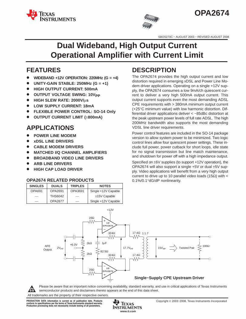
Single−Supply CPE Upstream Driver
82.5Ω2kΩ
2kΩ 1µF
17.4Ω
100Ω2VPP
AFEOutput
324Ω
20Ω
324Ω
1/2O PA 2674
1/2O PA 2674
+12V
1:1.7
15VPP Twisted Pair17.7VPP
20Ω
17.4Ω
+6.0V
! !
OPA2674
SBOS270C − AUGUST 2003 − REVISED AUGUST 2008
Dual Wideband, High Output CurrentOperational Amplifier with Current Limit
www.ti.com
Copyright 2003−2008, Texas Instruments Incorporated
Please be aware that an important notice concerning availability, standard warranty, and use in critical applications of Texas Instrumentssemiconductor products and disclaimers thereto appears at the end of this data sheet.
All trademarks are the property of their respective owners.
"#$%SBOS270C − AUGUST 2003 − REVISED AUGUST 2008
www.ti.com
2
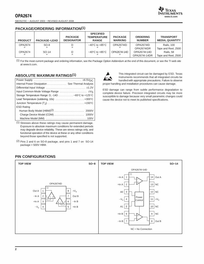
PACKAGE/ORDERING INFORMATION (1)
PRODUCT PACKAGE−LEADPACKAGE
DESIGNATOR
SPECIFIEDTEMPERATURE
RANGEPACKAGEMARKING
ORDERINGNUMBER
TRANSPORTMEDIA, QUANTITY
OPA2674 SO-8 D −40°C to +85°C OPA2674ID OPA2674ID Rails, 100″ ″ ″ ″ ″ OPA2674IDR Tape and Reel, 2500
OPA2674 SO-14 D −40°C to +85°C OPA2674I-14D OPA2674I-14D Rails, 58″ ″ ″ ″ ″ OPA2674I-14DR Tape and Reel, 2500
(1) For the most current package and ordering information, see the Package Option Addendum at the end of this document, or see the TI web siteat www.ti.com.
ABSOLUTE MAXIMUM RATINGS (1)
Power Supply ±6.5VDC. . . . . . . . . . . . . . . . . . . . . . . . . . . . . . . . . . . Internal Power Dissipation See Thermal Analysis. . . . . . . . . . . . . . Differential Input Voltage ±1.2V. . . . . . . . . . . . . . . . . . . . . . . . . . . . . Input Common-Mode Voltage Range ±VS. . . . . . . . . . . . . . . . . . . . Storage Temperature Range: D, -14D −65°C to +125°C. . . . . . . . . . . Lead Temperature (soldering, 10s) +300°C. . . . . . . . . . . . . . . . . . . . .
Junction Temperature (TJ) +150°C. . . . . . . . . . . . . . . . . . . . . . . . . . . ESD Rating Human Body Model (HBM)(2) 2000V. . . . . . . . . . . . . . . . . . . . . . Charge Device Model (CDM) 1000V. . . . . . . . . . . . . . . . . . . . . . Machine Model (MM) 100V. . . . . . . . . . . . . . . . . . . . . . . . . . . . . .
(1) Stresses above these ratings may cause permanent damage.Exposure to absolute maximum conditions for extended periodsmay degrade device reliability. These are stress ratings only, andfunctional operation of the device at these or any other conditionsbeyond those specified is not supported.
(2) Pins 2 and 6 on SO-8 package, and pins 1 and 7 on SO-14package > 500V HBM.
This integrated circuit can be damaged by ESD. TexasInstruments recommends that all integrated circuits behandled with appropriate precautions. Failure to observe
proper handling and installation procedures can cause damage.
ESD damage can range from subtle performance degradation tocomplete device failure. Precision integrated circuits may be moresusceptible to damage because very small parametric changes couldcause the device not to meet its published specifications.
PIN CONFIGURATIONS
NC = No Connection
1
2
3
4
8
7
6
5
+VS
Out B
−In B
+In B
OPA2674ID
Out A
−In A
+In A
−VS
1
2
3
4
5
6
7
14
13
12
11
10
9
8
−In A
+In A
A0
−VS
A1
+In B
−In B
Out A
NC
NC
+VS
NC
NC
Out B
PowerControl
OPA2674I−14D
TOP VIEW SO−8 TOP VIEW SO−14

"#$%SBOS270C − AUGUST 2003 − REVISED AUGUST 2008
www.ti.com
3
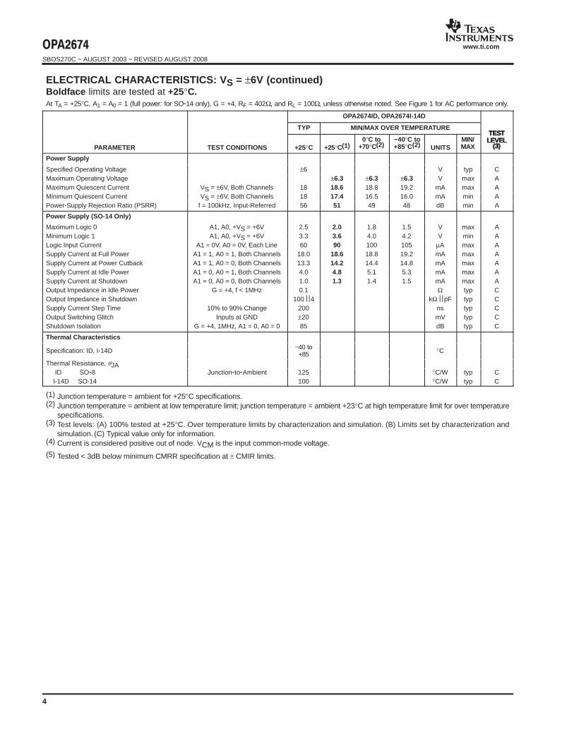
ELECTRICAL CHARACTERISTICS: V S = ±6V Boldface limits are tested at +25°C.At TA = +25°C, A1 = A0 = 1 (full power: for SO-14 only), G = +4, RF = 402Ω, and RL = 100Ω, unless otherwise noted. See Figure 1 for AC performance only.
OPA2674ID, OPA2674I-14D
TYP MIN/MAX OVER TEMPERATURETEST
PARAMETER TEST CONDITIONS +25°C +25°C(1)0°C to
+70°C(2)−40°C to+85°C(2) UNITS
MIN/MAX
TESTLEVEL
(3)
AC Performance (see Figure 1)Small-Signal Bandwidth (VO = 0.5VPP) G = +1, RF = 511Ω 250 MHz typ CSmall-Signal Bandwidth (VO = 0.5VPP)
G = +2, RF = 475Ω 225 170 165 160 MHz min BG = +4, RF = 402Ω 220 170 165 160 MHz min BG = +8, RF = 250Ω 260 200 195 190 MHz min B
Peaking at a Gain of +1 G = +1, RF = 511Ω 0.2 dB typ CBandwidth for 0.1dB Gain Flatness G = +4, VO = 0.5VPP 100 40 35 30 MHz min BLarge-Signal Bandwidth G = +4, VO = 5VPP 220 160 155 150 MHz typ CSlew Rate G = +4, 5V step 2000 1500 1450 1400 V/µs min BRise Time and Fall Time G = +4, VO = 2V step 1.6 ns typ CHarmonic Distortion G = +4, f = 5MHz, VO = 2VPP 2nd-Harmonic RL = 100Ω −72 −68 −67 −66 dBc max B
RL ≥ 500Ω −82 −80 −79 −78 dBc max B 3rd-Harmonic RL = 100Ω −81 −79 −78 −77 dBc max B
RL ≥ 500Ω −93 −91 −90 −89 dBc max BInput Voltage Noise f > 1MHz 2 2.6 2.9 3.1 nV/√Hz max BNoninverting Input Current Noise f > 1MHz 16 20 21 22 pA/√Hz max BInverting Input Current Noise f > 1MHz 24 29 30 31 pA/√Hz max BNTSC Differential Gain NTSC, G = +2, RL = 150Ω 0.03 % typ CNTSC Differential Gain
NTSC, G = +2, RL = 37.5Ω 0.05 % typ CNTCS Differential Phase NTSC, G = +2, RL = 150Ω 0.01 deg typ CNTCS Differential Phase
NTSC, G = +2, RL = 37.5Ω 0.04 deg typ CChannel-to-Channel Crosstalk f = 5MHz, Input-Referred −92 dB typ C
DC Performance (4)
Open-Loop Transimpedance Gain VO = 0V, RL = 100Ω 135 80 76 75 kΩ min AInput Offset Voltage VCM = 0V ±1 ±4.5 ±5 ±5.3 mV max AOffset Voltage Drift VCM = 0V ±4 ±10 ±10 ±12 µV/°C max BNoninverting Input Bias Current VCM = 0V ±10 ±30 ±32 ±35 µA max ANoninverting Input Bias Current Drift VCM = 0V ±5 ±50 ±50 ±75 nA/°C max BInverting Input Bias Current VCM = 0V ±10 ±35 ±40 ±45 µA max AInverting Input Bias Current Drift VCM = 0V ±10 ±100 ±100 ±150 nA/°C max B
Input (4)
Common-Mode Input Range (CMIR)(5) ±4.5 ±4.1 ±4.0 ±4.0 V min ACommon-Mode Rejection Ratio (CMRR) VCM = 0V, Input-Referred 55 51 50 50 dB min ANoninverting Input Impedance 250 2 kΩ pF typ CMinimum Inverting Input Resistance Open-Loop 22 12 Ω min BMaximum Inverting Input Resistance Open-Loop 22 35 Ω max B
Output (4)
Output Voltage Swing No Load ±5.1 ±4.9 ±4.8 ±4.7 V min AOutput Voltage SwingRL = 100Ω ±5.0 ±4.8 ±4.7 ±4.5 V min ARL = 25Ω ±4.8 V typ C
Current Output VO = 0 ±500 ±380 ±350 ±320 mA min AShort-Circuit Current VO = 0 ±800 mA typ CClosed-Loop Output Impedance G = +4, f ≤ 100kHz 0.01 Ω typ C
Output (4) (SO-14 Only)
Current Output at Full Power A1 = 1, A0 = 1, VO = 0 ±500 ±380 ±350 ±320 mA min ACurrent Output at Power Cutback A1 = 1, A0 = 0, VO = 0 ±450 ±350 ±320 ±300 mA min ACurrent Output at Idle Power A1 = 0, A0 = 1, VO = 0 ±100 ±60 ±55 ±50 mA min A
(1) Junction temperature = ambient for +25°C specifications.(2) Junction temperature = ambient at low temperature limit; junction temperature = ambient +23°C at high temperature limit for over temperature
specifications.(3) Test levels: (A) 100% tested at +25°C. Over temperature limits by characterization and simulation. (B) Limits set by characterization and
simulation. (C) Typical value only for information.(4) Current is considered positive out of node. VCM is the input common-mode voltage.
(5) Tested < 3dB below minimum CMRR specification at ± CMIR limits.
"#$%SBOS270C − AUGUST 2003 − REVISED AUGUST 2008
www.ti.com
4
ELECTRICAL CHARACTERISTICS: V S = ±6V (continued)Boldface limits are tested at +25°C.At TA = +25°C, A1 = A0 = 1 (full power: for SO-14 only), G = +4, RF = 402Ω, and RL = 100Ω, unless otherwise noted. See Figure 1 for AC performance only.
TESTLEVEL
(3)
OPA2674ID, OPA2674I-14D
TESTLEVEL
(3)
MIN/MAX OVER TEMPERATURETYP
PARAMETER
TESTLEVEL
(3)MIN/MAXUNITS
−40°C to+85°C(2)
0°C to+70°C(2)+25°C(1)+25°CTEST CONDITIONS
Power Supply
Specified Operating Voltage ±6 V typ CMaximum Operating Voltage ±6.3 ±6.3 ±6.3 V max AMaximum Quiescent Current VS = ±6V, Both Channels 18 18.6 18.8 19.2 mA max AMinimum Quiescent Current VS = ±6V, Both Channels 18 17.4 16.5 16.0 mA min APower-Supply Rejection Ratio (PSRR) f = 100kHz, Input-Referred 56 51 49 48 dB min A
Power Supply (SO-14 Only)
Maximum Logic 0 A1, A0, +VS = +6V 2.5 2.0 1.8 1.5 V max AMinimum Logic 1 A1, A0, +VS = +6V 3.3 3.6 4.0 4.2 V min ALogic Input Current A1 = 0V, A0 = 0V, Each Line 60 90 100 105 µA max ASupply Current at Full Power A1 = 1, A0 = 1, Both Channels 18.0 18.6 18.8 19.2 mA max ASupply Current at Power Cutback A1 = 1, A0 = 0, Both Channels 13.3 14.2 14.4 14.8 mA max ASupply Current at Idle Power A1 = 0, A0 = 1, Both Channels 4.0 4.8 5.1 5.3 mA max ASupply Current at Shutdown A1 = 0, A0 = 0, Both Channels 1.0 1.3 1.4 1.5 mA max AOutput Impedance in Idle Power G = +4, f < 1MHz 0.1 Ω typ COutput Impedance in Shutdown 100 4 kΩ pF typ CSupply Current Step Time 10% to 90% Change 200 ns typ COutput Switching Glitch Inputs at GND ±20 mV typ CShutdown Isolation G = +4, 1MHz, A1 = 0, A0 = 0 85 dB typ C
Thermal Characteristics
Specification: ID, I-14D −40 to+85 °C
Thermal Resistance, JA ID SO-8 Junction-to-Ambient 125 °C/W typ C I-14D SO-14 100 °C/W typ C
(1) Junction temperature = ambient for +25°C specifications.(2) Junction temperature = ambient at low temperature limit; junction temperature = ambient +23°C at high temperature limit for over temperature
specifications.(3) Test levels: (A) 100% tested at +25°C. Over temperature limits by characterization and simulation. (B) Limits set by characterization and
simulation. (C) Typical value only for information.(4) Current is considered positive out of node. VCM is the input common-mode voltage.
(5) Tested < 3dB below minimum CMRR specification at ± CMIR limits.

"#$%SBOS270C − AUGUST 2003 − REVISED AUGUST 2008
www.ti.com
5
ELECTRICAL CHARACTERISTICS: V S = +5V Boldface limits are tested at +25°C.At TA = +25°C, A1 = 1, A0 = 1 (Full Power: for SO-14 only), G = +4, RF = 453Ω, and RL = 100Ω, unless otherwise noted. See Figure 3 for ACperformance only.
OPA2674ID, OPA2674I-14D
TYP MIN/MAX OVER TEMPERATURETEST
PARAMETER TEST CONDITIONS +25°C +25°C(1) 0°C to+70°C(2)
−40°C to+85°C(2) UNITS MIN/
MAX
TESTLEVEL
(3)
AC Performance (see Figure 3)
Small-Signal Bandwidth (VO = 0.5VPP) G = +1, RF = 536Ω 220 MHz typ CSmall-Signal Bandwidth (VO = 0.5VPP)G = +2, RF = 511Ω 175 140 130 120 MHz min BG = +4, RF = 453Ω 168 130 126 120 MHz min BG = +8, RF = 332Ω 175 140 130 125 MHz min B
Peaking at a Gain of +1 G = +1, RF = 511Ω 0.6 dB typ CBandwidth for 0.1dB Gain Flatness G = +4, VO = 0.5VPP 34 24 22 20 MHz min BLarge-Signal Bandwidth G = +4, VO = 5VPP 190 140 135 130 MHz typ CSlew Rate G = +4, 2V Step 900 650 625 600 V/µs min BRise Time and Fall Time G = +4, VO = 2V Step 2 ns typ CHarmonic Distortion G = +4, f = 5MHz, VO = 2VPP 2nd-Harmonic RL = 100Ω −65 −63 −62 −61 dBc max B
RL ≥ 500Ω −72 −70 −69 −68 dBc max B 3rd-Harmonic RL = 100Ω −72 −70 −69 −68 dBc max B
RL ≥ 500Ω −74 −71 −70 −69 dBc max BInput Voltage Noise f > 1MHz 2 2.6 2.9 3.1 nV/√Hz max BNoninverting Input Current Noise f > 1MHz 16 20 21 22 pA/√Hz max BInverting Input Current Noise f > 1MHz 24 29 30 31 pA/√Hz max B
Channel-to-Channel Crosstalk f = 5MHz, Input-Referred −92 dB typ C
DC Performance (4)
Open-Loop Transimpedance Gain VO = 0V, RL = 100Ω 110 72 70 68 kΩ min AInput Offset Voltage VCM = 0V ±0.8 ±3.5 ±4.0 ±4.3 mV max AOffset Voltage Drift VCM = 0V ±4 ±10 ±10 ±12 µV/°C max BNoninverting Input Bias Current VCM = 0V ±10 ±30 ±32 ±35 µA max ANoninverting Input Bias Current Drift VCM = 0V ±5 ±50 ±50 ±75 nA/°C max BInverting Input Bias Current VCM = 0V ±10 ±35 ±40 ±45 µA max AInverting Input Bias Current Drift VCM = 0V ±10 ±100 ±100 ±150 nA/°C max B
Input
Most Positive Input Voltage(5) 3.7 3.3 3.2 3.1 V min AMost Negative Input Voltage(5) 1.3 1.7 1.8 1.9 V min A
Common-Mode Rejection Ratio (CMRR) VCM = 2.5V, Input-Referred 53 49 48 47 dB min A
Noninverting Input Impedance 250 2 kΩ pF typ C
Minimum Inverting Input Resistance Open-Loop 25 15 Ω min B
Maximum Inverting Input Resistance Open-Loop 25 40 Ω max B
Output
Most Positive Output Voltage No Load 4.1 3.9 3.8 3.6 V min AMost Positive Output VoltageRL = 100Ω 3.9 3.8 3.7 3.5 V min A
Most Negative Output Voltage No Load 0.8 1.0 1.1 1.3 V max AMost Negative Output VoltageRL = 100Ω 1.0 1.1 1.2 1.5 V max A
Current Output VO = 0 ±260 ±200 ±180 ±160 mA min AClosed-Loop Output Impedance G = +4, f ≤ 100kHz 0.02 Ω typ C
Output (SO-14 Only)
Current Output at Full Power A1 = 1, A0 = 1, VO = 0 ±260 ±200 ±180 ±160 mA min ACurrent Output at Power Cutback A1 = 1, A0 = 0, VO = 0 ±200 ±160 ±140 ±120 mA min ACurrent Output at Idle Power A1 = 0, A0 = 1, VO = 0 ±80 ±50 ±45 ±40 mA min A
(1) Junction temperature = ambient for +25°C specifications.(2) Junction temperature = ambient at low temperature limit; junction temperature = ambient +23°C at high temperature limit for over temperature
specifications.(3) Test levels: (A) 100% tested at +25°C. Over temperature limits by characterization and simulation. (B) Limits set by characterization and
simulation. (C) Typical value only for information.(4) Current considered positive out of node. VCM is the input common-mode voltage.(5) Tested < 3dB below minimum CMRR at min/max input ranges.

"#$%SBOS270C − AUGUST 2003 − REVISED AUGUST 2008
www.ti.com
6
ELECTRICAL CHARACTERISTICS: V S = +5V(continued)Boldface limits are tested at +25°C.At TA = +25°C, A1 = 1, A0 = 1 (Full Power: for SO-14 only), G = +4, RF = 453Ω, and RL = 100Ω, unless otherwise noted. See Figure 3 for ACperformance only.
TESTLEVEL
(3)
OPA2674ID, OPA2674I-14D
TESTLEVEL
(3)
MIN/MAX OVER TEMPERATURETYP
PARAMETER
TESTLEVEL
(3)MIN/MAXUNITS−40°C to
+85°C(2)0°C to
+70°C(2)+25°C(1)+25°CTEST CONDITIONS
Power Supply (Single−Supply Mode)
Specified Operating Voltage +5 V typ CMaximum Operating Voltage 12.6 12.6 12.6 V max AMaximum Quiescent Current VS = +5V, Both Channels 13.6 14.8 15.2 15.6 mA max AMinimum Quiescent Current VS = +5V, Both Channels 13.6 12 11.7 11.4 mA min APower-Supply Rejection Ratio (PSRR) f = 100kHz, Input-Referred 52 dB typ C
Power Control (SO-14 Only)
Maximum Logic 0 A1, A0, +VS = +5V 1.5 1.0 0.9 0.8 V max A
Minimum Logic 1 A1, A0, +VS = +5V 2.4 2.7 3.1 3.3 V min A
Logic Input Current A1 = 0V, A0 = 0V, Each Line 50 80 90 95 µA max A
Supply Current at Full Power A1 = 1, A0 = 1, Both Channels 13.8 14.8 15.2 15.6 mA max A
Supply Current at Power Cutback A1 = 1, A0 = 0, Both Channels 10.2 10.8 11.1 11.4 mA max A
Supply Current at Idle Power A1 = 1, A0 = 1, Both Channels 3.0 3.2 3.5 3.8 mA max A
Supply Current at Shutdown A1 = 0, A0 = 0, Both Channels 0.6 0.9 1.0 1.1 mA max A
Output Impedance in Idle Power G = +4, f = 1MHz Ω typ C
Output Impedance in Shutdown 100 4 kΩ pF typ C
Supply Current Step Time 10% to 90% Change 200 ns typ C
Output Switching Glitch Inputs at GND ±20 mV typ C
Shutdown Isolation G = +4, 1MHz, A1 = 0, A0 = 0 85 dB typ C
Thermal Characteristics
Specification: ID, I-14D −40 to+85 °C
Thermal Resistance, JA ID SO-8 Junction-to-Ambient 125 °C/W typ C I-14D SO-14 100 °C/W typ C
(1) Junction temperature = ambient for +25°C specifications.(2) Junction temperature = ambient at low temperature limit; junction temperature = ambient +23°C at high temperature limit for over temperature
specifications.(3) Test levels: (A) 100% tested at +25°C. Over temperature limits by characterization and simulation. (B) Limits set by characterization and
simulation. (C) Typical value only for information.(4) Current considered positive out of node. VCM is the input common-mode voltage.(5) Tested < 3dB below minimum CMRR at min/max input ranges.
"#$%SBOS270C − AUGUST 2003 − REVISED AUGUST 2008
www.ti.com
7
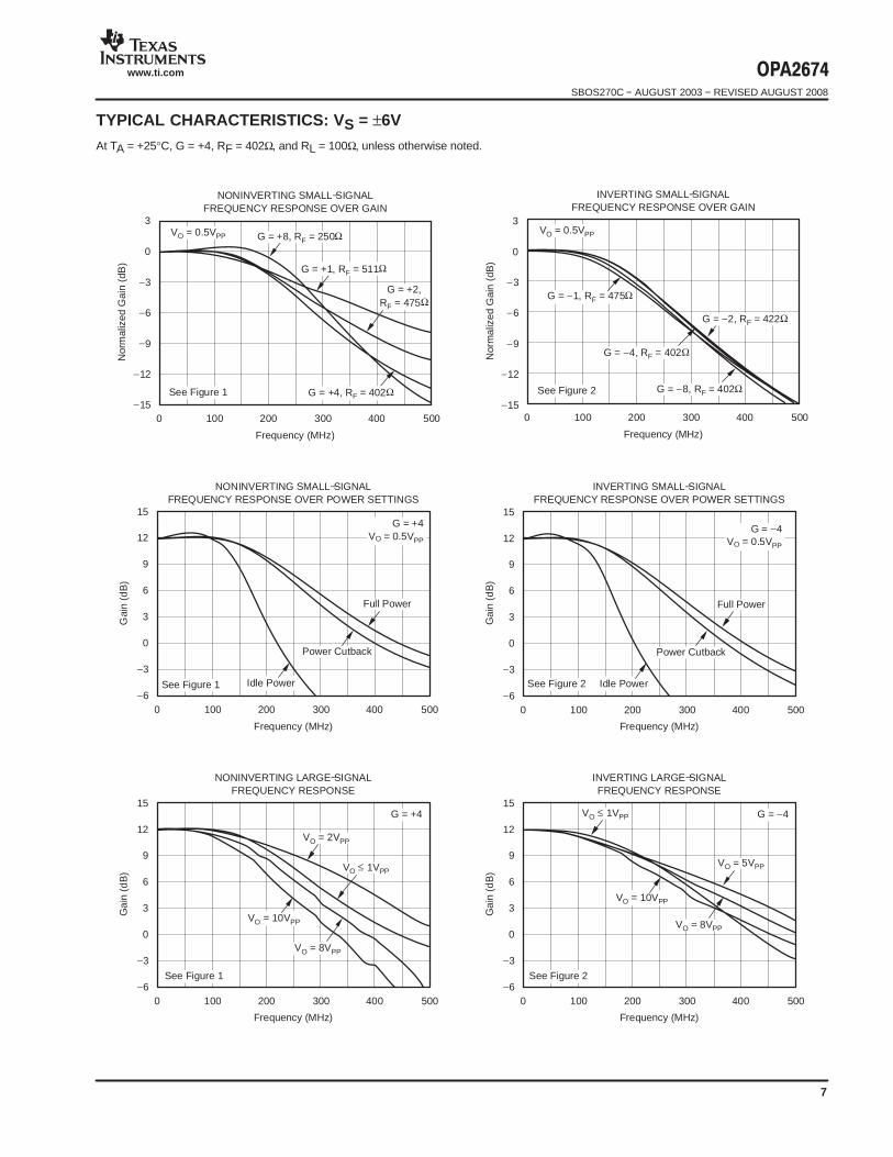
TYPICAL CHARACTERISTICS: V S = ±6V
At TA = +25°C, G = +4, RF = 402Ω, and RL = 100Ω, unless otherwise noted.
NONINVERTING SMALL−SIGNALFREQUENCY RESPONSE OVER GAIN
Frequency (MHz)
0 100 200 300 400 500
3
0
−3
−6
−9
−12
−15
Nor
mal
ized
Gai
n(d
B)
VO = 0.5VPP
See Figure 1
G = +8, RF = 250Ω
G = +2,RF = 475Ω
G = +4, RF = 402Ω
G = +1, RF = 511Ω
INVERTING SMALL−SIGNALFREQUENCY RESPONSE OVER GAIN
Frequency (MHz)
0 100 200 300 400 500
3
0
−3
−6
−9
−12
−15
Nor
mal
ized
Gai
n(d
B)
VO = 0.5VPP
See Figure 2
G = −1, RF = 475Ω
G = −2, RF = 422Ω
G = −8, RF = 402Ω
G = −4, RF = 402Ω
NONINVERTING SMALL−SIGNALFREQUENCY RESPONSE OVER POWER SETTINGS
Frequency (MHz)
0 100 200 300 400 500
15
12
9
6
3
0
−3
−6
Gai
n(d
B)
G = +4VO = 0.5VPP
Power Cutback
Idle Power
Full Power
See Figure 1
INVERTING SMALL−SIGNALFREQUENCY RESPONSE OVER POWER SETTINGS
Frequency (MHz)
0 100 200 300 400 500
15
12
9
6
3
0
−3
−6
Ga
in(d
B)
G = −4VO = 0.5VPP
Power Cutback
Idle Power
Full Power
See Figure 2
NONINVERTING LARGE−SIGNALFREQUENCY RESPONSE
Frequency (MHz)
0 100 200 300 400 500
15
12
9
6
3
0
−3
−6
Ga
in(d
B)
G = +4
VO = 8VPP
VO = 10VPP
VO = 2VPP
VO ≤ 1VPP
See Figure 1
INVERTING LARGE−SIGNALFREQUENCY RESPONSE
Frequency (MHz)
0 100 200 300 400 500
15
12
9
6
3
0
−3
−6
Ga
in(d
B)
G = −4
VO = 8VPP
VO = 10VPP
VO = 5VPP
VO ≤ 1VPP
See Figure 2
"#$%SBOS270C − AUGUST 2003 − REVISED AUGUST 2008
www.ti.com
8
TYPICAL CHARACTERISTICS: V S = ±6V (continued)
At TA = +25°C, G = +4, RF = 402Ω, and RL = 100Ω, unless otherwise noted.
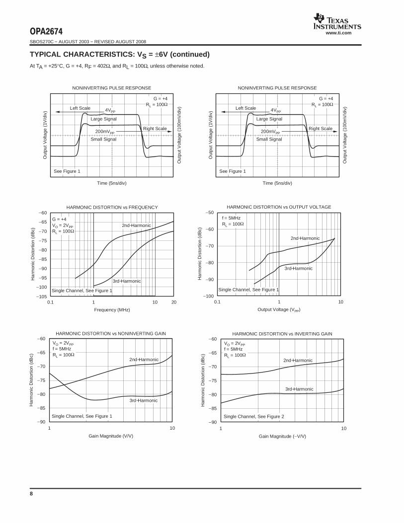
NONINVERTING PULSE RESPONSE
Time (5ns/div)
Out
put
Vo
ltage
(1V
/div
)
Out
put
Vol
tage
(100
mV
/div
)
4VPP
G = +4RL = 100Ω
200mVPP
Left Scale
Large Signal
Right Scale
Small Signal
See Figure 1
NONINVERTING PULSE RESPONSE
Time (5ns/div)
Out
put
Vo
ltage
(1V
/div
)
Out
put
Vol
tage
(100
mV
/div
)
4VPP
G = +4RL = 100Ω
200mVPP
Left Scale
Large Signal
Right Scale
Small Signal
See Figure 1
HARMONIC DISTORTION vs FREQUENCY
Frequency (MHz)
0.1 1 2010
−60
−65
−70
−75
−80
−85
−90
−95
−100
−105
Ha
rmon
icD
isto
rtio
n(d
Bc)
G = +4VO = 2VPPRL = 100Ω
Single Channel, See Figure 1
2nd−Harmonic
3rd−Harmonic
HARMONIC DISTORTION vs OUTPUT VOLTAGE
Output Voltage (VPP)
0.1 1 10
−50
−60
−70
−80
−90
−100
Har
mon
icD
isto
rtio
n(d
Bc)
f = 5MHzRL = 100Ω
2nd−Harmonic
3rd−Harmonic
Single Channel, See Figure 1
HARMONIC DISTORTION vs NONINVERTING GAIN
Gain Magnitude (V/V)
1
−60
−65
−70
−75
−80
−85
−9010
Har
mon
icD
isto
rtio
n(d
Bc)
VO = 2VPPf = 5MHzRL = 100Ω
2nd−Harmonic
3rd−Harmonic
Single Channel, See Figure 1
HARMONIC DISTORTION vs INVERTING GAIN
Gain Magnitude (−V/V)
1
−60
−65
−70
−75
−80
−85
−9010
Har
mon
icD
isto
rtio
n(d
Bc)
VO = 2VPPf = 5MHzRL = 100Ω
2nd−Harmonic
3rd−Harmonic
Single Channel, See Figure 2
"#$%SBOS270C − AUGUST 2003 − REVISED AUGUST 2008
www.ti.com
9
TYPICAL CHARACTERISTICS: V S = ±6V (continued)
At TA = +25°C, G = +4, RF = 402Ω, and RL = 100Ω, unless otherwise noted.
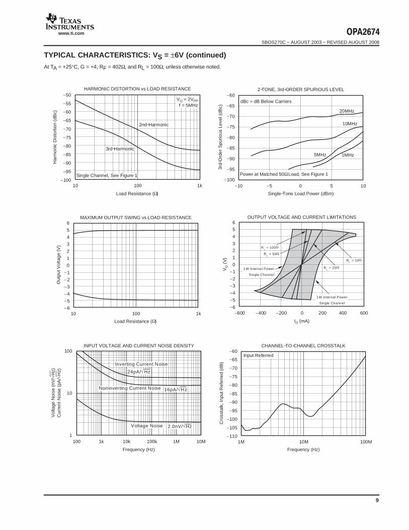
HARMONIC DISTORTION vs LOAD RESISTANCE
Load Resistance (Ω)
10
−50
−55
−60
−65
−70
−75
−80
−85
−90
−95
−100100 1k
Ha
rmo
nic
Dis
tort
ion
(dB
c)
Single Channel, See Figure 1
VO = 2VPPf = 5MHz
2nd−Harmonic
3rd−Harmonic
2−TONE, 3rd−ORDER SPURIOUS LEVEL
Single−Tone Load Power (dBm)
−10 0 5−5 10
−60
−65
−70
−75
−80
−85
−90
−95
−100
3rd−
Ord
er
Spu
rious
Leve
l(dB
c)
20MHz
5MHz 1MHz
Power at Matched 50ΩLoad, See Figure 1
10MHz
dBc = dB Below Carriers
MAXIMUM OUTPUT SWING vs LOAD RESISTANCE
Load Resistance (Ω)
10 100 1k
6
5
4
3
2
1
0
−1
−2
−3
−4
−5−6
Out
putV
olta
ge
(V)
OUTPUT VOLTAGE AND CURRENT LIMITATIONS
IO (mA)
−600
6
5
4
3
2
1
0
−1
−2−3
−4
−5
−60 200 400−200−400 600
VO
(V)
RL
= 10Ω
RL
= 25Ω
RL
= 50Ω
RL
= 100Ω
1W Interna l Power
Single Channel
1W Internal Power
Single Channel
INPUT VOLTAGE AND CURRENT NOISE DENSITY
Frequency (Hz)
100
100
10
1100k 1M10k1k 10M
Vo
ltage
Noi
se(n
V/√
Hz)
Cu
rren
tNoi
se(p
A/√
Hz)
Inverting Current Noise
Noninverting Current Noise
Voltage Noise 2.0nV/√Hz
16pA/√Hz
24pA/√ Hz
CHANNEL−TO−CHANNEL CROSSTALK
Frequency (Hz)
1M 10M 100M
−60
−65
−70
−75
−80
−85
−90
−95
−100
−105
−110
Cro
ssta
lk,I
nput
Ref
erre
d(d
B)
Input Referred
"#$%SBOS270C − AUGUST 2003 − REVISED AUGUST 2008
www.ti.com
10
TYPICAL CHARACTERISTICS: V S = ±6V (continued)
At TA = +25°C, G = +4, RF = 402Ω, and RL = 100Ω, unless otherwise noted.
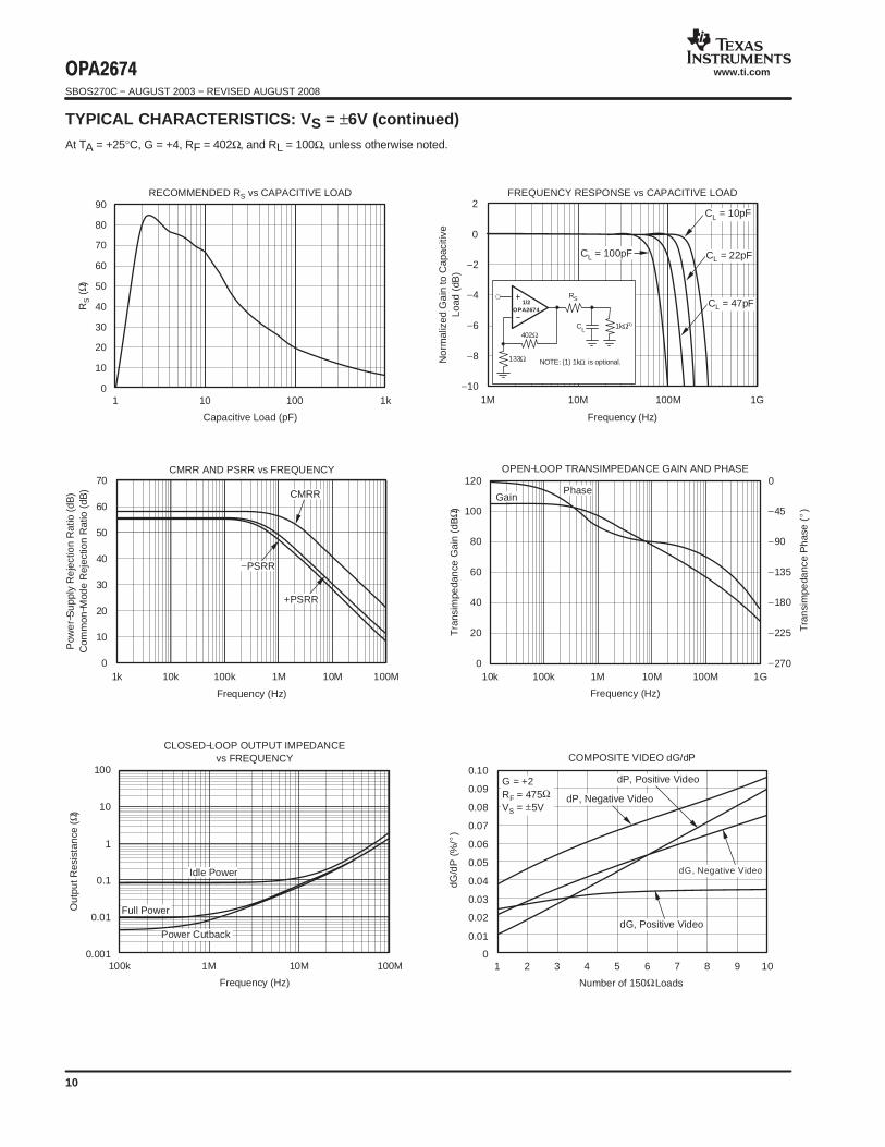
RECOMMENDED RS vs CAPACITIVE LOAD
Capacitive Load (pF)
1 10 100 1k
90
80
70
60
50
40
30
20
10
0
RS
(Ω)
FREQUENCY RESPONSE vs CAPACITIVE LOAD
Frequency (Hz)
1M
2
0
−2
−4
−6
−8
−1010M 100M 1G
No
rmal
ized
Ga
into
Cap
aciti
veL
oad
(dB
)
CL = 10pF
CL = 22pFCL = 100pF
CL = 47pF1/2OPA2674
402Ω
RS
133Ω
1kΩ(1)CL
NOTE: (1) 1kΩ is optional.
CMRR AND PSRR vs FREQUENCY
Frequency (Hz)
1k
70
60
50
40
30
20
10
010k 100k 1M 10M 100M
Pow
er−
Su
pply
Re
ject
ion
Rat
io(d
B)
Com
mon
−Mod
eR
ejec
tion
Rat
io(d
B) CMRR
−PSRR
+PSRR
OPEN−LOOP TRANSIMPEDANCE GAIN AND PHASE
Frequency (Hz)
10k 100k 1M 10M 100M 1G
120
100
80
60
40
20
0
Tra
nsim
peda
nce
Ga
in(d
BΩ )
0
−45
−90
−135
−180
−225
−270
Tra
nsi
mpe
danc
eP
has
e(
)
GainPhase
CLOSED−LOOP OUTPUT IMPEDANCEvs FREQUENCY
Frequency (Hz)
100k 1M 10M 100M
100
10
1
0.1
0.01
0.001
Out
putR
esis
tan
ce(Ω
)
Idle Power
Full Power
Power Cutback
COMPOSITE VIDEO dG/dP
Number of 150ΩLoads
1 2 3 4 5 6 7 8 9 10
0.10
0.09
0.08
0.07
0.06
0.05
0.04
0.03
0.02
0.01
0
dG/d
P(%
/)
G = +2RF = 475ΩVS = ±5V
dP, Negative Video
dP, Positive Video
dG, Positive Video
dG, Negative Video

"#$%SBOS270C − AUGUST 2003 − REVISED AUGUST 2008
www.ti.com
11
TYPICAL CHARACTERISTICS: V S = ±6V (continued)
At TA = +25°C, G = +4, RF = 402Ω, and RL = 100Ω, unless otherwise noted.
16
12
8
4
0
−4
−8
−12
−16
NONINVERTING OVERDRIVE RECOVERY
Time (25ns/div)
Ou
tput
Vol
tage
(V)
4
3
2
1
0
−1
−2
−3
−4
Inpu
tV
olta
ge(V
)
G = +4RL = 100ΩSee Figure 1
Input
Output
16
12
8
4
0
−4
−8
−12
−16
INVERTING OVERDRIVE RECOVERY
Time (25ns/div)
Out
putV
olta
ge(V
)
4
3
2
1
0
−1
−2
−3
−4
Inpu
tV
olta
ge(V
)
Input
Output
G = −4RL = 100Ω
See Figure 2
TYPICAL DC DRIFT OVER TEMPERATURE
Ambient Temperature (C)
−50
14121086420
−2−4−6−8
−10−12−14
−25 0 25 50 75 100 125
Inp
utO
ffse
tVo
ltag
e(m
V)
Inp
utB
ias
Cur
rent
(µA
) Noninverting Bias Current
Input Offset Voltage
Inverting Bias Current
SUPPLY AND OUTPUT CURRENT vs TEMPERATURE
Temperature (C)
−50
750
700
650
600
550
500
450
400
350
300
250−25 0 25 50 75 100 125
Ou
tput
Cu
rre
nt(m
A)
20
18
16
14
12
10
8
6
4
2
0
Su
pply
Cu
rren
t,B
oth
Cha
nnel
s(m
A)
Sourcing Output Current
Sinking Output Current
Supply Current, Full Power
Supply Current, Power Cutback
Supply Current, Idle Power
COMMON−MODE INPUT VOLTAGE RANGEAND OUTPUT SWING vs SUPPLY VOLTAGE
Supply Voltage (±V)
2 3 4 5
6
5
4
3
2
1
06
Vol
tag
eR
ange
(±V
)
Negative Output Swing
Negative Common−Mode Input Voltage
Positive Common−Mode Input Voltage
Positive Output Swing

"#$%SBOS270C − AUGUST 2003 − REVISED AUGUST 2008
www.ti.com
12
TYPICAL CHARACTERISTICS: V S = ±6V
At TA = +25°C, Differential Gain = +9, RF = 300Ω, and RL = 70Ω, unless otherwise noted. See Figure 5 for AC performance only.
DIFFERENTIAL SMALL−SIGNALFREQUENCY RESPONSE
Frequency (MHz)
0 25050 100 150 200 300
3
0
−3
−6
−9
−12
−15
No
rmal
ize
dG
ain
(dB
)
RL = 70ΩVO = 1VPP
See Figure 5
GD = +2,RF = 442Ω
GD = +5,RF = 383Ω
GD = +9,RF = 300Ω
DIFFERENTIAL LARGE−SIGNALFREQUENCY RESPONSE
Frequency (MHz)
0 25050 100 150 200 300
22
19
16
13
10
7
4
1
Gai
n(d
B)
16VPP
RL = 70ΩGD = +9
See Figure 5
8VPP4VPP
1VPP
DIFFERENTIAL DISTORTION vs LOAD RESISTANCE
Load Resistance (Ω)
10 1k100
−60
−65
−70
−75
−80
−85
−90
−95
−100
−105
−110
Har
mo
nic
Dis
tort
ion
(dB
)
2nd−Harmonic
3rd−Harmonic
f = 500kHzG = +9
RL = 70ΩVO = 4VPP
See Figure 5
DIFFERENTIAL DISTORTION vs FREQUENCY
Frequency (MHz)
0.1 101 100
−50
−65
−70
−80
−90
−100
−110
Har
mon
icD
isto
rtio
n(d
B)
2nd−Harmonic
3rd−Harmonic
G = +9RL = 70Ω
See Figure 5
DIFFERENTIAL DISTORTION vs OUTPUT VOLTAGE
Differential Output Voltage (VPP)
0.1 101 20
−60
−70
−80
−90
−100
−110
Ha
rmo
nic
Dis
tort
ion
(dB
c)
f = 500kHzG = +9RL = 70Ω
2nd−Harmonic
3rd−Harmonic
See Figure 5
ADSL MULTITONE POWER RATIO(Upstream)
Frequency (kHz)
0 4020 8060 120 140100 160
0
−10
−20
−30
−40
−50
−60
−70
−80
−90
−100
Po
wer
(dB
m)
VS = ±6V
See Figure 5

"#$%SBOS270C − AUGUST 2003 − REVISED AUGUST 2008
www.ti.com
13
TYPICAL CHARACTERISTICS: V S = +5V
At TA = +25°C, G = +4, RF = 453Ω, and RL = 100Ω, unless otherwise noted.
NONINVERTING SMALL−SIGNALFREQUENCY RESPONSE
Frequency (MHz)
0 100 200 300 400 500
3
0
−3
−6
−9
−12
−15
−18
Nor
mal
ized
Gai
n(d
B)
See Figure 3
G = +1RF = 549Ω
G = +2RF = 511Ω
G = +4RF = 453Ω
G = +8RF = 332Ω
INVERTING SMALL−SIGNALFREQUENCY RESPONSE
Frequency (MHz)
0 100 200 300 400 500
3
0
−3
−6
−9
−12
−15
−18
Nor
mal
ized
Gai
n(d
B)
See Figure 4
G = −1RF = 549Ω
G = −2RF = 511Ω
G = −4RF = 453Ω
G = −8RF = 402Ω
NONINVERTING LARGE−SIGNALFREQUENCY RESPONSE
Frequency (MHz)
0 100 200 300 400 500
15
12
9
6
3
0
−3
−6
Gai
n(d
B)
VO = 3VPP
VO = 1VPP
VO = 2VPP
G = +4RL = 100Ω to VS/2
See Figure 3
INVERTING LARGE−SIGNALFREQUENCY RESPONSE
Frequency (MHz)
0 100 200 300 400 500
15
12
9
6
3
0
−3
−6
Gai
n(d
B)
VO = 3VPP
VO = 1VPP
VO = 2VPP
G = −4RL = 100Ω to VS/2
See Figure 4
NONINVERTING PULSE RESPONSE
Time (5ns/div)
Out
putV
olta
ge
(0.5
V/d
iv)
Inpu
tVol
tag
e(1
00m
V/d
iv)2VPP Large Signal
200mVPP Small Signal
Left Scale
Right Scale
G = +4RL = 100Ω to VS/2 See Figure 3
INVERTING PULSE RESPONSE
Time (5ns/div)
Out
putV
olta
ge
(0.5
V/d
iv)
Inpu
tVol
tag
e(1
00m
V/d
iv)2VPP Large Signal
200mVPP Small Signal
Left Scale
Right Scale
G = −4RL = 100Ω to VS/2 See Figure 4
"#$%SBOS270C − AUGUST 2003 − REVISED AUGUST 2008
www.ti.com
14
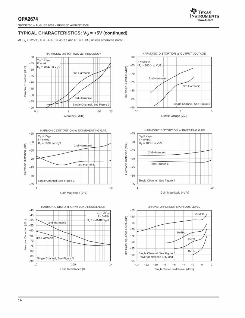
TYPICAL CHARACTERISTICS: V S = +5V (continued)
At TA = +25°C, G = +4, RF = 453Ω, and RL = 100Ω, unless otherwise noted.
HARMONIC DISTORTION vs FREQUENCY
Frequency (MHz)
0.1 1 2010
−50
−55
−60
−65
−70
−75
−80
−85
−90
Har
mo
nic
Dis
tort
ion
(dB
c)
VO = 2VPPG = +4RL = 100Ω to VS/2
Single Channel, See Figure 3
2nd−Harmonic
3rd−Harmonic
HARMONIC DISTORTION vs OUTPUT VOLTAGE
Output Voltage (VPP)
0.1 1 5
−60
−65
−70
−75
−80
−85
−90
Har
mon
icD
isto
rtio
n(d
Bc)
f = 5MHzRL = 100Ω to VS/2
Single Channel, See Figure 3
3rd−Harmonic
2nd−Harmonic
HARMONIC DISTORTION vs NONINVERTING GAIN
Gain Magnitude (V/V)
1
−55
−60
−65
−70
−75
−80
−8510
Ha
rmon
icD
isto
rtio
n(d
Bc) 2nd−Harmonic
3rd−Harmonic
VO = 2VPPf = 5MHzRL = 100Ω to VS/2
Single Channel, See Figure 3
HARMONIC DISTORTION vs INVERTING GAIN
Gain Magnitude (−V/V)
1
−55
−60
−65
−70
−75
−80
−8510
Ha
rmon
icD
isto
rtio
n(d
Bc)
2nd−Harmonic
3rd−Harmonic
VO = 2VPPf = 5MHzRL = 100Ω to VS/2
Single Channel, See Figure 4
HARMONIC DISTORTION vs LOAD RESISTANCE
Load Resistance (Ω)
10 100 1k
−40
−45
−50
−55
−60
−65
−70
−75
−80
−85
−90
Ha
rmon
icD
isto
rtio
n(d
Bc)
Single Channel, See Figure 3
VO = 2VPPf = 5MHz
RL = 100Ω to VS/22nd−Harmonic
3rd−Harmonic
2−TONE, 3rd−ORDER SPURIOUS LEVEL
Single−Tone Load Power (dBm)
−14 −6 −2−10 2−8 −4−12 0
−55
−60
−65
−70
−75
−80
−85
−90
−95
3rd
−Ord
erS
pur
ious
Leve
l(dB
c)
Single Channel. See Figure 3.Power at matched 50Ω load.
20MHz
5MHz
1MHz
10MHz
"#$%SBOS270C − AUGUST 2003 − REVISED AUGUST 2008
www.ti.com
15
TYPICAL CHARACTERISTICS: V S = +5V
At TA = +25°C, Differential Gain = +9, RF = 316Ω, and RL = 70Ω, unless otherwise noted.
DIFFERENTIAL PERFORMANCETEST CIRCUIT
R L
R F31 6Ω
R G
C G
R F31 6Ω
V OV I
GD = 1 +2 × RF
RG=
VO
VI
+5V
DIFFERENTIAL SMALL−SIGNALFREQUENCY RESPONSE
Frequency (MHz)
0 50 100 150 200 250 300
3
0
−3
−6
−9
−12
−15
Nor
ma
lized
Gai
n(d
B)
GD = +2RF = 511Ω
GD = +5RF = 422Ω
GD = +9RF = 316Ω
RL = 70Ω
DIFFERENTIAL LARGE−SIGNALFREQUENCY RESPONSE
Frequency (MHz)
0 50 100 150 200 250 300
22
19
16
13
10
7
4
1
Gai
n(d
B)
4VPP1VPP
2VPP5VPP
RL = 70ΩGD = +9
HARMONIC DISTORTION vs LOAD RESISTANCE
Load Resistance (Ω)
10 1k100
−60
−65
−70
−75
−80
−85
−90
−95
−100
Har
mon
icD
isto
rtio
n(d
Bc) 2nd−Harmonic
3rd−Harmonic
GD = +9RL = 70Ω
f = 500kHzVO = 4VPP
DIFFERENTIAL DISTORTION vs FREQUENCY
Frequency (MHz)
0.1 101 100
−50
−60
−70
−80
−90
−100
Ha
rmo
nic
Dis
tort
ion
(dB
c)
3rd−Harmonic
2nd−Harmonic
GD = +9RL = 70Ω
HARMONIC DISTORTION vs OUTPUT VOLTAGE
Output Voltage (VPP)
1 10
−60
−70
−80
−90
−100
Ha
rmon
icD
isto
rtio
n(d
B)
GD = +9RL = 70Ωf = 500kHz
2nd−Harmonic
3rd−Harmonic

"#$%SBOS270C − AUGUST 2003 − REVISED AUGUST 2008
www.ti.com
16
APPLICATION INFORMATIONWIDEBAND CURRENT-FEEDBACK OPERATION
The OPA2674 gives the exceptional AC performance of awideband current-feedback op amp with a highly linear,high-power output stage. Requiring only 9mA/ch quies-cent current, the OPA2674 swings to within 1V of eithersupply rail and delivers in excess of 380mA at room tem-perature. This low output headroom requirement, alongwith supply voltage independent biasing, gives remark-able single (+5V) supply operation. The OPA2674 deliversgreater than 150MHz bandwidth driving a 2VPP output into100Ω on a single +5V supply. Previous boosted outputstage amplifiers typically suffer from very poor crossoverdistortion as the output current goes through zero. TheOPA2674 achieves a comparable power gain with muchbetter linearity. The primary advantage of a current-feed-back op amp over a voltage-feedback op amp is that ACperformance (bandwidth and distortion) is relatively inde-pendent of signal gain. Figure 1 shows the DC-coupled,gain of +4, dual power-supply circuit configuration used asthe basis of the ±6V Electrical and Typical Characteristics.For test purposes, the input impedance is set to 50Ω witha resistor to ground and the output impedance is set to 50Ωwith a series output resistor. Voltage swings reported in theelectrical characteristics are taken directly at the input andoutput pins whereas load powers (dBm) are defined at amatched 50Ω load. For the circuit of Figure 1, the total ef-fective load is 100Ω || 535Ω = 84Ω.
1/2OPA2674
+6V
+
−6V
50ΩLoad
50Ω50ΩVOVI
50ΩSource
RG133Ω
RF402Ω
+
6.8µF
0.1µF 6.8µF
0.1µF
+VS
−VS
Figure 1. DC-Coupled, G = +4, Bipolar Supply,Specification and Test Circuit
Figure 2 shows the DC-coupled, bipolar supply circuit in-verting gain configuration used as the basis for the ±6VElectrical and Typical Characteristics. Key design consid-erations of the inverting configuration are developed in theInverting Amplifier Operation discussion.
1/2OPA2674
+6V
−6V
50ΩLoad50ΩVO
VI
50ΩSource
RM100Ω
RF402Ω
RG100Ω
Power−supplydecouplingnot shown.
Figure 2. DC-Coupled, G = −4, Bipolar Supply,Specification and Test Circuit
Figure 3 shows the AC-coupled, gain of +4, single-supplycircuit configuration used as the basis of the +5V Electricaland Typical Characteristics. Though not a rail-to-rail de-sign, the OPA2674 requires minimal input and output volt-age headroom compared to other wideband current-feed-back op amps. It will deliver a 3VPP output swing on asingle +5V supply with greater than 100MHz bandwidth.The key requirement of broadband single- supply opera-tion is to maintain input and output signal swings within theusable voltage ranges at both the input and the output. Thecircuit of Figure 3 establishes an input midpoint bias usinga simple resistive divider from the +5V supply (two 806Ωresistors). The input signal is then AC-coupled into thismidpoint voltage bias. The input voltage can swing to with-in 1.3V of either supply pin, giving a 2.4VPP input signalrange centered between the supply pins. The input imped-ance matching resistor (57.6Ω) used for testing is adjustedto give a 50Ω input match when the parallel combinationof the biasing divider network is included. The gain resistor(RG) is AC-coupled, giving the circuit a DC gain of+1which puts the input DC bias voltage (2.5V) on theoutput as well. The feedback resistor value is adjustedfrom the bipolar supply condition to re-optimize for a flatfrequency response in +5V, gain of +4, operation. Again,on a single +5V supply, the output voltage can swing towithin 1V of either supply pin while delivering more than200mA output current. A demanding 100Ω load to a mid-point bias is used in this characterization circuit. The newoutput stage used in the OPA2674 can deliver large bipolaroutput currents into this midpoint load with minimal cross-over distortion, as shown by the +5V supply, harmonic dis-tortion plots in the Typical Characteristics charts.
"#$%SBOS270C − AUGUST 2003 − REVISED AUGUST 2008
www.ti.com
17
1/2OPA2674
+5V+VS
VS/2806Ω
100ΩVOVI 57.6Ω
806Ω
RF453Ω
RG150Ω
0.1µF
0.1µF
6.8µF+
0.1µF
Figure 3. AC-Coupled, G = +4, Single-Supply,Specification and Test Circuit
The last configuration used as the basis of the +5V Electri-cal and Typical Characteristics is shown in Figure 4. De-sign considerations for this inverting, bipolar supply config-uration are covered either in single-supply configuration(as shown in Figure 3) or in the Inverting Amplifier Opera-tion discussion.
1/2OPA2674
+5V
VS/2806Ω
VI
100ΩVO
806Ω
RF453Ω
RM88.7Ω
6.8µF+
0.1µF
0.1µFRG
113Ω
Figure 4. AC-Coupled, G = −4, Single-Supply,Specification and Test Circuit
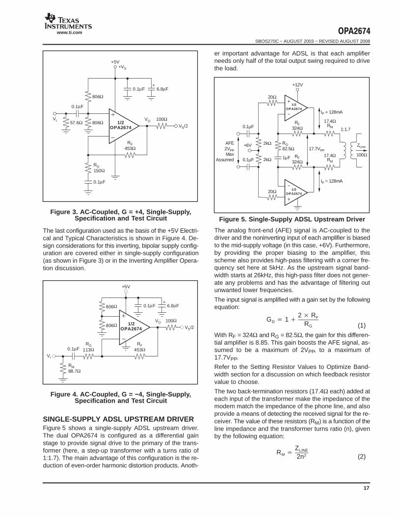
SINGLE-SUPPLY ADSL UPSTREAM DRIVERFigure 5 shows a single-supply ADSL upstream driver.The dual OPA2674 is configured as a differential gainstage to provide signal drive to the primary of the trans-former (here, a step-up transformer with a turns ratio of1:1.7). The main advantage of this configuration is the re-duction of even-order harmonic distortion products. Anoth-
er important advantage for ADSL is that each amplifierneeds only half of the total output swing required to drivethe load.
RG82.5Ω
2kΩ
2kΩ
1µF
0.1µF
0.1µF17.4Ω
RM
100Ω
AFE2VPPMax
Assumed
RF324Ω
20Ω
20Ω
RF324Ω
1/2OPA2674
1/2OPA2674
+12V
1:1.7
17.7VPP
IP = 128mA
IP = 128mA
17.4ΩRM
+6V ZLine
Figure 5. Single-Supply ADSL Upstream Driver
The analog front-end (AFE) signal is AC-coupled to thedriver and the noninverting input of each amplifier is biasedto the mid-supply voltage (in this case, +6V). Furthermore,by providing the proper biasing to the amplifier, thisscheme also provides high-pass filtering with a corner fre-quency set here at 5kHz. As the upstream signal band-width starts at 26kHz, this high-pass filter does not gener-ate any problems and has the advantage of filtering outunwanted lower frequencies.
The input signal is amplified with a gain set by the followingequation:
GD 1 2 RF
RG
With RF = 324Ω and RG = 82.5Ω, the gain for this differen-tial amplifier is 8.85. This gain boosts the AFE signal, as-sumed to be a maximum of 2VPP, to a maximum of17.7VPP.
Refer to the Setting Resistor Values to Optimize Band-width section for a discussion on which feedback resistorvalue to choose.
The two back-termination resistors (17.4Ω each) added ateach input of the transformer make the impedance of themodem match the impedance of the phone line, and alsoprovide a means of detecting the received signal for the re-ceiver. The value of these resistors (RM) is a function of theline impedance and the transformer turns ratio (n), givenby the following equation:
RM ZLINE
2n2
(1)
(2)
"#$%SBOS270C − AUGUST 2003 − REVISED AUGUST 2008
www.ti.com
18
OPA2674 HDSL2 UPSTREAM DRIVER
Figure 6 shows an HDSL2 implementation of a single-supply driver.
82.5Ω
2kΩ
2kΩ
1µF
0.1µF
0.1µF 11.5Ω135Ω
AFE2VPPMax
Assumed
324Ω
20Ω
20Ω
324Ω
1/2OPA2674
1/2OPA2674
+12V
1:2.4
17.7VPP
IP = 185mA
IP = 185mA
11.5Ω
+6V ZLine
Figure 6. HDSL2 Upstream DriverThe two designs differ by the values of the matching im-pedance, the load impedance, and the ratio turns of thetransformers. All of these differences are reflected in thehigher peak current and thus, the higher maximum powerdissipation in the output of the driver.
LINE DRIVER HEADROOM MODEL
The first step in a driver design is to compute the peak-to-peak output voltage from the target specifications. This isdone using the following equations:
PL 10 logVRMS
2
(1mW) RL
With PL power and VRMS voltage at the load, and RL loadimpedance, this gives:
VRMS (1mW) RL 10PL10
VP CrestFactor VRMS CF VRMS
with VP peak voltage at the load and CF Crest Factor;
VLPP 2 CF VRMS
with VLPP: peak-to-peak voltage at the load.
Consolidating Equations 3 through 6 allows the requiredpeak-to-peak voltage at the load function of the crest fac-tor, the load impedance, and the power in the load to be ex-pressed. Thus:
VLPP 2 CF (1mW) RL 10PL10
This VLPP is usually computed for a nominal line imped-ance and may be taken as a fixed design target.
The next step for the driver is to compute the individual am-plifier output voltage and currents as a function of VPP onthe line and transformer turns ratio. As the turns ratiochanges, the minimum allowed supply voltage alsochanges. The peak current in the amplifier is given by:
IP 12
2 VLPP
n 1
4RM
With VLPP defined in Equation 7 and RM defined in Equa-tion 2. The peak current is computed in Figure 7 by notingthat the total load is 4RM and that the peak current is halfof the peak-to-peak calculated using VLPP.
RM
RM
VLPPn VLPPRL
±IP
±IP
2VLPPn
1:n
Figure 7. Driver Peak Output Model
With the required output voltage and current versus turnsratio set, an output stage headroom model will allow the re-quired supply voltage versus turns ratio to be developed.
The headroom model (see Figure 8) can be described withthe following set of equations:
First, as available output voltage for each amplifier:
VOPP VCC (V1 V2) IP (R1 R2)
Or, second, as required single-supply voltage:
VCC VOPP (V1 V2) IP (R1 R2)
The minimum supply voltage for a power and load require-ment is given by Equation 10.
(3)
(4)
(5)
(6)
(7)
(8)
(9)
(10)

"#$%SBOS270C − AUGUST 2003 − REVISED AUGUST 2008
www.ti.com
19
VO
R1
V1
+VCC
R2
V2
IP
Figure 8. Line Driver Headroom ModelTable 1 gives V1, V2, R1, and R2 for both +12V and +5V op-eration of the OPA2674.
Table 1. Line Driver Headroom Model Values
V1 R1 V2 R2
+5V 0.9V 5Ω 0.8V 5Ω
+12V 0.9V 2Ω 0.9V 2Ω
TOTAL DRIVER POWER FOR xDSLAPPLICATIONS
The total internal power dissipation for the OPA2674 in anxDSL line driver application will be the sum of the quies-cent power and the output stage power. The OPA2674holds a relatively constant quiescent current versus supplyvoltage—giving a power contribution that is simply thequiescent current times the supply voltage used (the sup-ply voltage will be greater than the solution given in Equa-tion 10). The total output stage power may be computedwith reference to Figure 9.
RT
+VCCIAVG =
IPCF
Figure 9. Output Stage Power ModelThe two output stages used to drive the load of Figure 7can be seen as an H-Bridge in Figure 9. The average cur-rent drawn from the supply into this H-Bridge and load will
be the peak current in the load given by Equation 8 dividedby the crest factor (CF) for the xDSL modulation. This totalpower from the supply is then reduced by the power in RTto leave the power dissipated internal to the drivers in thefour output stage transistors. That power is simply the tar-get line power used in Equation 2 plus the power lost in thematching elements (RM). In the examples here, a perfectmatch is targeted giving the same power in the matchingelements as in the load. The output stage power is then setby Equation 11.
POUT IP
CF VCC 2PL
The total amplifier power is then:
PTOT Iq VCC IP
CF VCC 2PL
For the ADSL CPE upstream driver design of Figure 5, thepeak current is 128mA for a signal that requires a crest fac-tor of 5.33 with a target line power of 13dBm into 100Ω(20mW). With a typical quiescent current of 18mA and anominal supply voltage of +12V, the total internal powerdissipation for the solution of Figure 5 will be:
PTOT 18mA(12V) 128mA5.33
(12V) 2(20mW) 464mW
DESIGN-IN TOOLSDEMONSTRATION FIXTURES
Two printed circuit boards (PCBs) are available to assistin the initial evaluation of circuit performance using theOPA2674 in its two package options. Both of these are of-fered free of charge as unpopulated PCBs, delivered witha user’s guide. The summary information for these fixturesis shown in Table 2.
Table 2. Demonstration Fixtures by Package
ORDERING LITERATURE
PRODUCT PACKAGE
ORDERING
NUMBER
LITERATURE
NUMBER
OPA2674ID SO-8 DEM-OPA-SO-2A SBOU003
OPA2674I-14D SO-14 DEM-OPA-SO-2D SBOU002
The demonstration fixtures can be requested at the TexasInstruments web site (www.ti.com) through the OPA2674product folder.
MACROMODELS AND APPLICATIONSSUPPORT
Computer simulation of circuit performance using SPICEis often useful when analyzing the performance of analogcircuits and systems. This is particularly true for video andRF amplifier circuits where parasitic capacitance and in-ductance can have a major effect on circuit performance.A SPICE model for the OPA2674 is available through the
(11)
(12)
(13)

"#$%SBOS270C − AUGUST 2003 − REVISED AUGUST 2008
www.ti.com
20
TI web site (www.ti.com). This model does a good job ofpredicting small-signal AC and transient performance un-der a wide variety of operating conditions, but does not doas well in predicting the harmonic distortion or dG/dP char-acteristics. This model does not attempt to distinguish be-tween the package types in small-signal AC performance,nor does it attempt to simulate channel-to- channel cou-pling.
OPERATING SUGGESTIONSSETTING RESISTOR VALUES TO OPTIMIZEBANDWIDTHA current-feedback op amp such as the OPA2674 can holdan almost constant bandwidth over signal gain settingswith the proper adjustment of the external resistor values,which are shown in the Typical Characteristics; the small-signal bandwidth decreases only slightly with increasinggain. These characteristic curves also show that the feed-back resistor is changed for each gain setting. The resistorvalues on the inverting side of the circuit for a current-feed-back op amp can be treated as frequency response com-pensation elements, whereas the ratios set the signal gain.Figure 10 shows the small-signal frequency responseanalysis circuit for the OPA2674.
VO
RG
VI
RI
Z(S) IERR
α
RF
IERR
Figure 10. Current-Feedback Transfer FunctionAnalysis Circuit
The key elements of this current-feedback op amp modelare:
α = buffer gain from the noninverting input to theinverting input
RI = buffer output impedance
IERR = feedback error current signal
Z(s) = frequency dependent open-loop transimpe-dance gain from IERR to VO
NG NoiseGain 1 RF
RG
The buffer gain is typically very close to 1.00 and is normal-ly neglected from signal gain considerations. This gain,however, sets the CMRR for a single op amp differentialamplifier configuration. For a buffer gain of α < 1.0, theCMRR = −20 • log(1 − α)dB.
RI, the buffer output impedance, is a critical portion of thebandwidth control equation. The OPA2674 inverting out-put impedance is typically 22Ω.
A current-feedback op amp senses an error current in theinverting node (as opposed to a differential input error volt-age for a voltage-feedback op amp) and passes this on tothe output through an internal frequency dependent trans-impedance gain. The Typical Characteristics show thisopen-loop transimpedance response, which is analogousto the open-loop voltage gain curve for a voltage-feedbackop amp. Developing the transfer function for the circuit ofFigure 10 gives Equation 14:
VO
VI
1 RFRG
1
RFRI1RFRG
Z(s)
NG
1 RFRING
Z(s)
This is written in a loop-gain analysis format, where the er-rors arising from a non-infinite open-loop gain are shownin the denominator. If Z(s) were infinite over all frequen-cies, the denominator of Equation 14 reduces to 1 and theideal desired signal gain shown in the numerator isachieved. The fraction in the denominator of Equation 14determines the frequency response. Equation 15 showsthis as the loop-gain equation:
Z(s)RF RI NG
LoopGain
If 20 log(RF + NG × RI) is drawn on top of the open-looptransimpedance plot, the difference between the twowould be the loop gain at a given frequency. Eventually,Z(s) rolls off to equal the denominator of Equation 15, atwhich point the loop gain has reduced to 1 (and the curveshave intersected). This point of equality is where the ampli-fier closed-loop frequency response given by Equation 14starts to roll off, and is exactly analogous to the frequencyat which the noise gain equals the open-loop voltage gainfor a voltage-feedback op amp. The difference here is thatthe total impedance in the denominator of Equation 15may be controlled somewhat separately from the desiredsignal gain (or NG). The OPA2674 is internally compen-sated to give a maximally flat frequency response for RF= 402Ω at NG = 4 on ±6V supplies. Evaluating the denomi-
(14)
(15)
"#$%SBOS270C − AUGUST 2003 − REVISED AUGUST 2008
www.ti.com
21
nator of Equation 15 (which is the feedback transimpe-dance) gives an optimal target of 490Ω. As the signal gainchanges, the contribution of the NG × RI term in the feed-back transimpedance changes, but the total can be heldconstant by adjusting RF. Equation 16 gives an approxi-mate equation for optimum RF over signal gain:
RF 490 NG RI
As the desired signal gain increases, this equation eventu-ally suggests a negative RF. A somewhat subjective limitto this adjustment can also be set by holding RG to a mini-mum value of 20Ω. Lower values load both the buffer stageat the input and the output stage if RF gets too lowactual-ly decreasing the bandwidth. Figure 11 shows the recom-mended RF versus NG for both ±6V and a single +5V op-eration. The values for RF versus gain shown here areapproximately equal to the values used to generate theTypical Characteristics. They differ in that the optimizedvalues used in the Typical Characteristics are also correct-ing for board parasitic not considered in the simplified anal-ysis leading to Equation 16. The values shown in Figure 11give a good starting point for designs where bandwidth op-timization is desired.
600
500
400
300
200
Noise Gain
0 2510 15 205
Fee
dbac
kR
esi
sto
r(Ω
)
+5V
RG = 20Ω
±6V
Figure 11. Feedback Resistor vs Noise Gain
The total impedance going into the inverting input may beused to adjust the closed-loop signal bandwidth. Insertinga series resistor between the inverting input and the sum-ming junction increases the feedback impedance (the de-nominator of Equation 15), decreasing the bandwidth. Theinternal buffer output impedance for the OPA2674 is slight-ly influenced by the source impedance coming from of thenoninverting input terminal. High-source resistors alsohave the effect of increasing RI, decreasing the bandwidth.For those single-supply applications that develop a mid-point bias at the noninverting input through high valued re-sistors, the decoupling capacitor is essential for power-supply ripple rejection, noninverting input noise currentshunting, and to minimize the high-frequency value for RIin Figure 10.
INVERTING AMPLIFIER OPERATION
As the OPA2674 is a general-purpose, wideband current-feedback op amp, most of the familiar op amp applicationcircuits are available to the designer. Those dual op ampapplications that require considerable flexibility in the feed-back element (for example, integrators, transimpedance,and some filters) should consider a unity-gain stable, volt-age-feedback amplifier such as the OPA2822, becausethe feedback resistor is the compensation element for acurrent-feedback op amp. Wideband inverting operation(and especially summing) is particularly suited to theOPA2674. Figure 12 shows a typical inverting configura-tion where the I/O impedances and signal gain fromFigure 1 are retained in an inverting circuit configuration.
1/2
O P A 267 4
RF392Ω
RG97.6Ω
+6V
−6V
50Ω50Ω Load
VO
Power−supplydecoupling notshown.
VI
50ΩSource
RM102Ω
Figure 12. Inverting Gain of −4 with ImpedanceMatching
In the inverting configuration, two key design consider-ations must be noted. First, the gain resistor (RG) becomespart of the signal source input impedance. If input imped-ance matching is desired (which is beneficial wheneverthe signal is coupled through a cable, twisted pair, longPCB trace, or other transmission line conductor), it is nor-mally necessary to add an additional matching resistor toground. RG, by itself, normally is not set to the required in-put impedance since its value, along with the desired gain,will determine an RF, which may be nonoptimal from a fre-quency response standpoint. The total input impedancefor the source becomes the parallel combination of RG andRM.
The second major consideration is that the signal sourceimpedance becomes part of the noise gain equation andhas a slight effect on the bandwidth through Equation 15.The values shown in Figure 12 have accounted for this byslightly decreasing RF (from the optimum values) to reopti-mize the bandwidth for the noise gain of Figure 12 (NG =3.98). In the example of Figure 12, the RM value combinesin parallel with the external 50Ω source impedance, yield-ing an effective driving impedance of 50Ω || 102Ω =
(16)
"#$%SBOS270C − AUGUST 2003 − REVISED AUGUST 2008
www.ti.com
22
33.5Ω. This impedance is added in series with RG for cal-culating the noise gainwhich gives NG = 3.98. This val-ue, and the inverting input impedance of 22Ω, are insertedinto Equation 16 to get the RF that appears in Figure 12.Note that the noninverting input in this bipolar supply in-verting application is connected directly to ground.
It is often suggested that an additional resistor be con-nected to ground on the noninverting input to achieve biascurrent error cancellation at the output. The input bias cur-rents for a current-feedback op amp are not generallymatched in either magnitude or polarity. Connecting a re-sistor to ground on the noninverting input of the OPA2674in the circuit of Figure 12 actually provides additional gainfor that input bias and noise currents, but does not de-crease the output DC error because the input bias currentsare not matched.
OUTPUT CURRENT AND VOLTAGE
The OPA2674 provides output voltage and current capa-bilities that are unsurpassed in a low-cost dual monolithicop amp. Under no-load conditions at 25°C, the output volt-age typically swings closer than 1V to either supply rail; thetested (+25°C) swing limit is within 1.1V of either rail. Intoa 6Ω load (the minimum tested load), it delivers more than±380mA.
The specifications described previously, though familiar inthe industry, consider voltage and current limits separately.In many applications, it is the voltage times current (or V−Iproduct) that is more relevant to circuit operation. Refer tothe Output Voltage and Current Limitations plot in the Typi-cal Characteristics (see page 9). The X and Y axes of thisgraph show the zero-voltage output current limit and thezero-current output voltage limit, respectively. The fourquadrants give a more detailed view of the OPA2674 out-put drive capabilities, noting that the graph is bounded bya safe operating area of 1W maximum internal power dis-sipation (in this case, for one channel only). Superimpos-ing resistor load lines onto the plot shows that theOPA2674 can drive ±4V into 10Ω or ±4.5V into 25Ω with-out exceeding the output capabilities or the 1W dissipationlimit. A 100Ω load line (the standard test circuit load)shows the full ±5.0V output swing capability, as stated inthe Electrical Characteristics tables. The minimum speci-fied output voltage and current over temperature are set byworst-case simulations at the cold temperature extreme.Only at cold startup will the output current and voltage de-crease to the numbers shown in the Electrical Characteris-tics tables. As the output transistors deliver power, thejunction temperatures increase, decreasing the VBEs (in-creasing the available output voltage swing), and increas-ing the current gains (increasing the available output cur-rent). In steady-state operation, the available outputvoltage and current will always be greater than that shownin the over-temperature specifications since the outputstage junction temperatures will be higher than the mini-mum specified operating ambient.
DRIVING CAPACITIVE LOADSOne of the most demanding and yet very common loadconditions for an op amp is capacitive loading. Often, thecapacitive load is the input of an analog-to-digital (A/D)converterincluding additional external capacitance thatmay be recommended to improve the A/D converter linear-ity. A high-speed, high open-loop gain amplifier like theOPA2674 can be very susceptible to decreased stabilityand closed-loop response peaking when a capacitive loadis placed directly on the output pin. When the amplifieropen-loop output resistance is considered, this capacitiveload introduces an additional pole in the signal path thatcan decrease the phase margin. Several external solu-tions to this problem have been suggested.
When the primary considerations are frequency responseflatness, pulse response fidelity, and/or distortion, the sim-plest and most effective solution is to isolate the capacitiveload from the feedback loop by inserting a series isolationresistor between the amplifier output and the capacitiveload. This does not eliminate the pole from the loop re-sponse, but rather shifts it and adds a zero at a higher fre-quency. The additional zero acts to cancel the phase lagfrom the capacitive load pole, thus increasing the phasemargin and improving stability. The Typical Characteristicsshow the Recommended RS vs Capacitive Load and theresulting frequency response at the load. Parasitic capaci-tive loads greater than 2pF can begin to degrade the per-formance of the OPA2674. Long PC board traces, un-matched cables, and connections to multiple devices caneasily cause this value to be exceeded. Always considerthis effect carefully, and add the recommended series re-sistor as close as possible to the OPA2674 output pin (seethe Board Layout Guidelines section).
DISTORTION PERFORMANCEThe OPA2674 provides good distortion performance intoa 100Ω load on ±6V supplies. It also provides exceptionalperformance into lighter loads and/or operating on a single+5V supply. Generally, until the fundamental signal reach-es very high frequency or power levels, the 2nd-harmonicdominates the distortion with a negligible 3rd-harmoniccomponent. Focusing then on the 2nd-harmonic, increas-ing the load impedance improves distortion directly. Re-member that the total load includes the feedback net-workin the noninverting configuration (see Figure 1),this is the sum of RF + RG; in the inverting configuration,it is RF. Also, providing an additional supply decoupling ca-pacitor (0.01µF) between the supply pins (for bipolar op-eration) improves the 2nd-order distortion slightly (3dB to6dB).
In most op amps, increasing the output voltage swing di-rectly increases harmonic distortion. The Typical Charac-teristics show the 2nd-harmonic increasing at a little lessthan the expected 2x rate, whereas the 3rd-harmonic in-creases at a little less than the expected 3x rate. Where thetest power doubles, the difference between it and the
"#$%SBOS270C − AUGUST 2003 − REVISED AUGUST 2008
www.ti.com
23
2nd-harmonic decreases less than the expected 6dB,whereas the difference between it and the 3rd-harmonicdecreases by less than the expected 12dB. This factoralso shows up in the 2-tone, 3rd-order intermodulationspurious (IM3) response curves. The 3rd-order spuriouslevels are extremely low at low-output power levels. Theoutput stage continues to hold them low even as the funda-mental power reaches very high levels. As the TypicalCharacteristics show, the spurious intermodulation pow-ers do not increase as predicted by a traditional interceptmodel. As the fundamental power level increases, the dy-namic range does not decrease significantly. For two tonescentered at 20MHz, with 10dBm/tone into a matched 50Ωload (that is, 2VPP for each tone at the load, which requires8VPP for the overall 2-tone envelope at the output pin), theTypical Characteristics show 67dBc difference betweenthe test-tone power and the 3rd-order intermodulation spu-rious levels. This exceptional performance improves fur-ther when operating at lower frequencies.
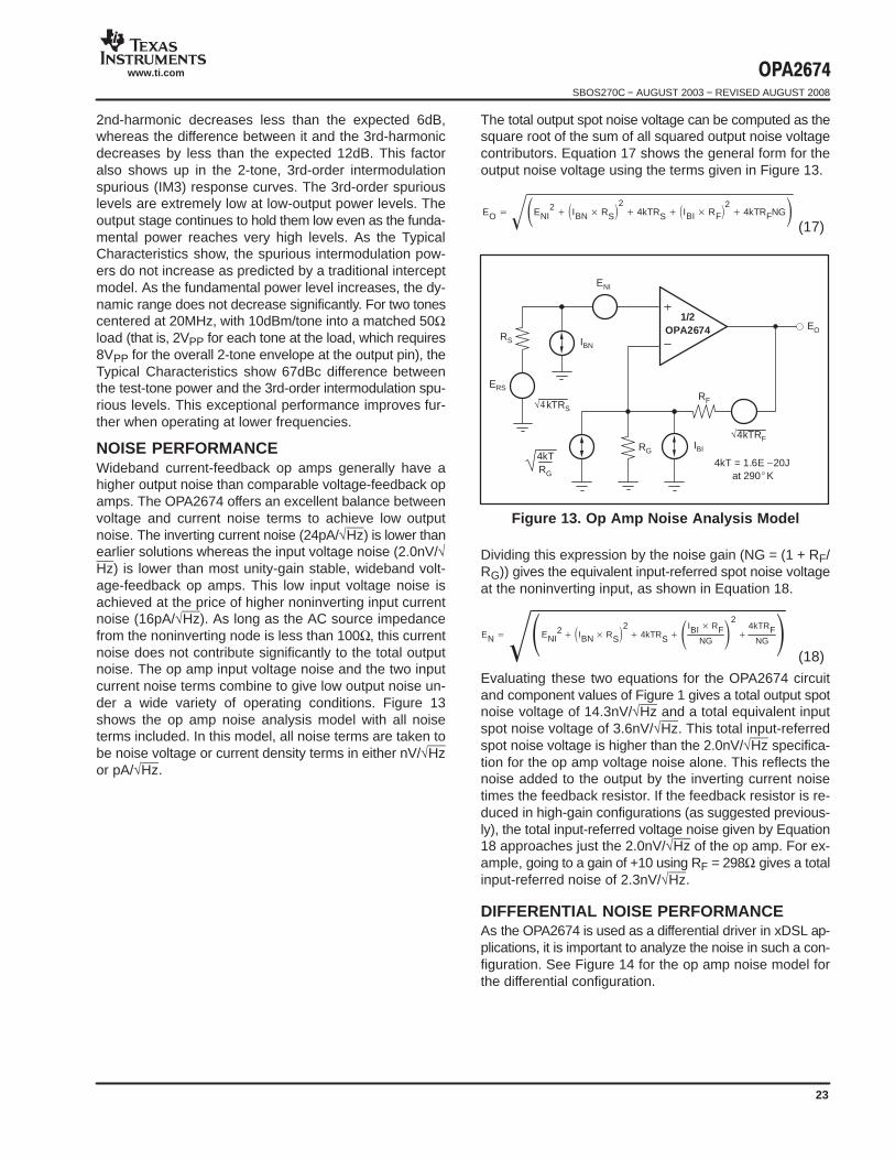
NOISE PERFORMANCEWideband current-feedback op amps generally have ahigher output noise than comparable voltage-feedback opamps. The OPA2674 offers an excellent balance betweenvoltage and current noise terms to achieve low outputnoise. The inverting current noise (24pA/√Hz) is lower thanearlier solutions whereas the input voltage noise (2.0nV/√Hz) is lower than most unity-gain stable, wideband volt-age-feedback op amps. This low input voltage noise isachieved at the price of higher noninverting input currentnoise (16pA/√Hz). As long as the AC source impedancefrom the noninverting node is less than 100Ω, this currentnoise does not contribute significantly to the total outputnoise. The op amp input voltage noise and the two inputcurrent noise terms combine to give low output noise un-der a wide variety of operating conditions. Figure 13shows the op amp noise analysis model with all noiseterms included. In this model, all noise terms are taken tobe noise voltage or current density terms in either nV/√Hzor pA/√Hz.
The total output spot noise voltage can be computed as thesquare root of the sum of all squared output noise voltagecontributors. Equation 17 shows the general form for theoutput noise voltage using the terms given in Figure 13.
EO ENI2 IBN RS
2 4kTRS IBI RF
2 4kTRFNG
4kTRG
RG
RF
RS
1/2OPA2674
IBI
EO
IBN
4kT = 1.6E −20Jat 290K
ERS
ENI
√4kTRS
√4kTRF
Figure 13. Op Amp Noise Analysis Model
Dividing this expression by the noise gain (NG = (1 + RF/RG)) gives the equivalent input-referred spot noise voltageat the noninverting input, as shown in Equation 18.
EN ENI2 IBN RS
2 4kTRS
IBI RFNG
2
4kTRFNG
Evaluating these two equations for the OPA2674 circuitand component values of Figure 1 gives a total output spotnoise voltage of 14.3nV/√Hz and a total equivalent inputspot noise voltage of 3.6nV/√Hz. This total input-referredspot noise voltage is higher than the 2.0nV/√Hz specifica-tion for the op amp voltage noise alone. This reflects thenoise added to the output by the inverting current noisetimes the feedback resistor. If the feedback resistor is re-duced in high-gain configurations (as suggested previous-ly), the total input-referred voltage noise given by Equation18 approaches just the 2.0nV/√Hz of the op amp. For ex-ample, going to a gain of +10 using RF = 298Ω gives a totalinput-referred noise of 2.3nV/√Hz.
DIFFERENTIAL NOISE PERFORMANCEAs the OPA2674 is used as a differential driver in xDSL ap-plications, it is important to analyze the noise in such a con-figuration. See Figure 14 for the op amp noise model forthe differential configuration.
(17)
(18)

"#$%SBOS270C − AUGUST 2003 − REVISED AUGUST 2008
www.ti.com
24
RG
RF
RS
EO2
Driver
ERS
EN
IN
II
√4kTRS
√4kTRF
RF
RS
ERS
EN
IN
II
√4kTRS
√4kTRG√4kTRF
Figure 14. Differential Op Amp Noise AnalysisModel
As a reminder, the differential gain is expressed as:
GD 1 2 RF
RG
The output noise voltage can be expressed as shown be-low:
eO2 2 GD
2eN
2 iN RS
2 4kTRS 2iIRF
2 24kTRFGD
Dividing this expression by the differential noise gain GD =(1 + 2RF/RG) gives the equivalent input-referred spot noisevoltage at the noninverting input, as shown in Equation 21.
eN 2 eN2iN RS
2 4kTRS 2iI
RFGD
2
24kTRF
GD
Evaluating this equation for the OPA2674 circuit and com-ponent values of Figure 5 gives a total output spot noisevoltage of 31.0nV/√Hz and a total equivalent input spotnoise voltage of 3.5nV/√Hz.
In order to minimize the noise contributed by IN, it is recom-mended to keep the noninverting source impedance aslow as possible.
DC ACCURACY AND OFFSET CONTROLA current-feedback op amp such as the OPA2674 pro-vides exceptional bandwidth in high gains, giving fastpulse settling but only moderate DC accuracy. The Electri-cal Characteristics show an input offset voltage compara-ble to high-speed, voltage-feedback amplifiers; however,the two input bias currents are somewhat higher and areunmatched. While bias current cancellation techniquesare very effective with most voltage-feedback op amps,they do not generally reduce the output DC offset for wide-band current-feedback op amps. Because the two inputbias currents are unrelated in both magnitude and polarity,matching the input source impedance to reduce error con-tribution to the output is ineffective. Evaluating the configu-ration of Figure 1, using worst-case +25°C input offset volt-age and the two input bias currents, gives a worst-caseoutput offset range equal to:
VOS = ± (NG × VIO(MAX)) ± (IBN × RS/2 × NG) ± (IBI × RF)
where NG = noninverting signal gain
= ± (4 × 4.5mV) ± (30µA × 25Ω × 4) ± (402Ω × 35µA)
= ±18mV ± 3mV ± 14mV
VOS = ±35.0mV (max at 25°C)
POWER CONTROL OPERATION (SO-14 ONLY)
The OPA2674I-14D provides a power control feature thatmay be used to reduce system power. The four modes ofoperation for this power control feature are full-power,power cutback, idle state, and power shutdown. Thesefour operating modes are set through two logic lines A0and A1. Table 3 shows the different modes of operation.
Table 3. Power Control Mode of Operation
MODE OFOPERATION A1 A0
Full-Power 1 1
Power Cutback 1 0
Idle State 0 1
Shutdown 0 0
The full-power mode is used for normal operating condi-tion. The power cutback mode brings the quiescent powerto 13.5mA. The idle state mode keeps a low output imped-ance but reduces output power and bandwidth. The shut-down mode has a high output impedance as well as thelowest quiescent power (1.0mA).
If the A0 and A1 pins are left unconnected, theOPA2674I-14D operates normally (full-power).
To change the power mode, the control pins (either A0 orA1) must be asserted low. This logic control is referencedto the positive supply, as shown in the simplified circuit ofFigure 15.
(19)
(20)
(21)

"#$%SBOS270C − AUGUST 2003 − REVISED AUGUST 2008
www.ti.com
25
46kΩ
60kΩ
1.2V120kΩ
Control −VS
+VS
A0 or A1 −VS
Q1Q2
Figure 15. Supply Power Control Circuit
The shutdown feature for the OPA2674 is a positive-sup-ply referenced, current-controlled interface. Open-collec-tor (or drain) interfaces are most effective, as long as thecontrolling logic can sustain the resulting voltage (in openmode) that appears at the A0 or A1 pins. The A0/A1 pinvoltage is one diode below the positive supply voltage ap-plied to the OPA2674 if the logic interface is open. For volt-age output logic interfaces, the on/off voltage levels de-scribed in the Electrical Characteristics apply only foreither the +6V used for the ±6V specifications or the +5Vfor the single-supply specifications. An open-drain inter-face is recommended to operate the A1 and A0 pins usinga higher positive supply and/or logic families with inade-quate high-level voltage swings.
THERMAL ANALYSISDue to the high output power capability of the OPA2674,heat-sinking or forced airflow may be required under ex-treme operating conditions. Maximum desired junctiontemperature sets the maximum allowed internal power dis-sipation, described below. In no case should the maximumjunction temperature be allowed to exceed 150°C.
Operating junction temperature (TJ) is given by TA + PD ×JA. The total internal power dissipation (PD) is the sum ofquiescent power (PDQ) and additional power dissipation inthe output stage (PDL) to deliver load power. Quiescentpower is the specified no-load supply current times the to-tal supply voltage across the part. PDL depends on the re-quired output signal and load. Using the example powercalculation for the ADSL CPE line driver concluded inEquation 13, and a worst-case analysis at +70°C ambient,the maximum internal junction temperature for the SO-8package will be:
TJ MAX = TAMBIENT + PMAX × 125°C/W
TJ MAX = 70°C + ((12V × 18.8mA) + 12V × 128mA/(5.33)− 40mW) × 125°C/W = 129°CThis maximum junction temperature is well below the max-imum of 150°C but may exceed system design targets.Lower junction temperature would be possible using the
SO-14 package and the power cutback feature. Repeatingthis calculation for that solution gives:
TJ MAX = 70°C + ((12V × 14.2mA) + 12V × 128mA/(5.33)− 40mW) × 100°C/W = 112°CFor extremely high internal power applications, where im-proved thermal performance is required, consider thePSO-8 package of the OPA2677—a similar part with nooutput stage current limit and a thermal impedance of lessthan 50°C/W.
BOARD LAYOUT GUIDELINESAchieving optimum performance with a high-frequencyamplifier like the OPA2674 requires careful attention toboard layout parasitic and external component types. Rec-ommendations that optimize performance include:
a) Minimize parasitic capacitance to any AC ground forall of the signal I/O pins. Parasitic capacitance on the out-put and inverting input pins can cause instability; on thenoninverting input, it can react with the source impedanceto cause unintentional band limiting. To reduce unwantedcapacitance, a window around the signal I/O pins shouldbe opened in all of the ground and power planes aroundthose pins. Otherwise, ground and power planes shouldbe unbroken elsewhere on the board.
b) Minimize the distance (< 0.25″) from the power-supplypins to high-frequency 0.1µF decoupling capacitors. At thedevice pins, the ground and power plane layout should notbe in close proximity to the signal I/O pins. Avoid narrowpower and ground traces to minimize inductance betweenthe pins and the decoupling capacitors. The power-supplyconnections (on pins 4 and 8 for an SO-8 package) shouldalways be decoupled with these capacitors. An optionalsupply decoupling capacitor across the two power supplies(for bipolar operation) improves 2nd-harmonic distortion per-formance. Larger (2.2µF to 6.8µF) decoupling capacitors,effective at a lower frequency, should also be used on themain supply pins. These can be placed somewhat fartherfrom the device and may be shared among several de-vices in the same area of the PC board.
c) Careful selection and pl acement of external compo-nents preserve the high-frequency performance of theOPA2674. Resistors should be of a very low reactancetype. Surface-mount resistors work best and allow a tighteroverall layout. Metal film and carbon composition axiallyleaded resistors can also provide good high-frequencyperformance. Again, keep the leads and PCB trace lengthas short as possible. Never use wire-wound type resistorsin a high-frequency application. Although the output pinand inverting input pin are the most sensitive to parasiticcapacitance, always position the feedback and series out-put resistor, if any, as close as possible to the output pin.Other network components, such as noninverting inputtermination resistors, should also be placed close to thepackage. Where double-side component mounting is al-lowed, place the feedback resistor directly under the pack-

"#$%SBOS270C − AUGUST 2003 − REVISED AUGUST 2008
www.ti.com
26
age on the other side of the board between the output andinverting input pins. The frequency response is primarilydetermined by the feedback resistor value as describedpreviously. Increasing the value reduces the bandwidth,whereas decreasing it gives a more peaked frequency re-sponse. The 402Ω feedback resistor used in the TypicalCharacteristics at a gain of +4 on ±6V supplies is a goodstarting point for design. Note that a 511Ω feedback resis-tor, rather than a direct short, is recommended for the uni-ty-gain follower application. A current-feedback op amp re-quires a feedback resistor even in the unity-gain followerconfiguration to control stability.
d) Connections to other wideband devices on the boardmay be made with short direct traces or through onboardtransmission lines. For short connections, consider thetrace and the input to the next device as a lumped capaci-tive load. Relatively wide traces (50mils to 100mils) shouldbe used, preferably with ground and power planes openedup around them. Estimate the total capacitive load and setRS from the plot of Recommended RS vs Capacitive Load(see page 10). Low parasitic capacitive loads (< 5pF) maynot need an RS because the OPA2674 is nominally com-pensated to operate with a 2pF parasitic load. If a longtrace is required, and the 6dB signal loss intrinsic to adoubly-terminated transmission line is acceptable, imple-ment a matched impedance transmission line using micro-strip or stripline techniques (consult an ECL design hand-book for microstrip and stripline layout techniques). A 50Ωenvironment is normally not necessary onboard. In fact, ahigher impedance environment improves distortion; seethe distortion versus load plots. With a characteristic boardtrace impedance defined based on board material andtrace dimensions, a matching series resistor into the tracefrom the output of the OPA2674 is used, as well as a termi-nating shunt resistor at the input of the destination device.Remember also that the terminating impedance is the par-allel combination of the shunt resistor and the input imped-ance of the destination device.
This total effective impedance should be set to match thetrace impedance. The high output voltage and current ca-pability of the OPA2674 allows multiple destination de-vices to be handled as separate transmission lines, eachwith their own series and shunt terminations. If the 6dB at-tenuation of a doubly-terminated transmission line is unac-
ceptable, a long trace can be series-terminated at thesource end only. Treat the trace as a capacitive load in thiscase, and set the series resistor value as shown in the plotof RS vs Capacitive Load. However, this does not preservesignal integrity as well as a doubly-terminated line. If theinput impedance of the destination device is low, there issome signal attenuation due to the voltage divider formedby the series output into the terminating impedance.
e) Socketing a high-speed part like the OPA2674 is notrecommended. The additional lead length and pin-to-pincapacitance introduced by the socket can create an ex-tremely troublesome parasitic network, which can make italmost impossible to achieve a smooth, stable frequencyresponse. Best results are obtained by soldering theOPA2674 onto the board.
INPUT AND ESD PROTECTIONThe OPA2674 is built using a high-speed complementarybipolar process. The internal junction breakdown voltagesare relatively low for these very small geometry devicesand are reflected in the absolute maximum ratings table.All device pins have limited ESD protection using internaldiodes to the power supplies, as shown in Figure 16.
These diodes provide moderate protection to input over-drive voltages above the supplies as well. The protectiondiodes can typically support 30mA continuous current.Where higher currents are possible (for example, in sys-tems with ±15V supply parts driving into the OPA2674),current-limiting series resistors should be added into thetwo inputs. Keep these resistor values as low as possible,because high values degrade both noise performance andfrequency response.
ExternalPin
+VCC
−VCC
InternalCircuitry
Figure 16. ESD Steering Diodes

SBOS270C − AUGUST 2003 − REVISED AUGUST 2008
www.ti.com
27
Revision History
DATE REV PAGE SECTION DESCRIPTION
8/08 C 2 Absolute Maximum Ratings Changed Storage Temperature minimum value from −40°C to −65°C.
3/08 B 4, 6 Electrical CharacteristicsAdded Both Channels; Power Supply and Power Supply (SO−14 only) sections under Conditons.
NOTE: Page numbers for previous revisions may differ from page numbers in the current version.
PACKAGE OPTION ADDENDUM
www.ti.com 15-Apr-2017
Addendum-Page 1
PACKAGING INFORMATION
Orderable Device Status(1)
Package Type PackageDrawing
Pins PackageQty
Eco Plan(2)
Lead/Ball Finish(6)
MSL Peak Temp(3)
Op Temp (°C) Device Marking(4/5)
Samples
HPA00088I-14DR ACTIVE SOIC D 14 2500 Green (RoHS& no Sb/Br)
CU NIPDAU Level-2-260C-1 YEAR -40 to 85 OPA2674
OPA2674I-14D ACTIVE SOIC D 14 50 Green (RoHS& no Sb/Br)
CU NIPDAU Level-2-260C-1 YEAR -40 to 85 OPA2674
OPA2674I-14DG4 ACTIVE SOIC D 14 50 Green (RoHS& no Sb/Br)
CU NIPDAU Level-2-260C-1 YEAR -40 to 85 OPA2674
OPA2674I-14DR ACTIVE SOIC D 14 2500 Green (RoHS& no Sb/Br)
CU NIPDAU Level-2-260C-1 YEAR -40 to 85 OPA2674
OPA2674I-14DRG4 ACTIVE SOIC D 14 2500 Green (RoHS& no Sb/Br)
CU NIPDAU Level-2-260C-1 YEAR -40 to 85 OPA2674
OPA2674ID ACTIVE SOIC D 8 75 Green (RoHS& no Sb/Br)
CU NIPDAU Level-2-260C-1 YEAR -40 to 85 OPA2674
OPA2674IDG4 ACTIVE SOIC D 8 75 Green (RoHS& no Sb/Br)
CU NIPDAU Level-2-260C-1 YEAR -40 to 85 OPA2674
OPA2674IDR ACTIVE SOIC D 8 2500 Green (RoHS& no Sb/Br)
CU NIPDAU Level-2-260C-1 YEAR -40 to 85 OPA2674
OPA2674IDRG4 ACTIVE SOIC D 8 2500 Green (RoHS& no Sb/Br)
CU NIPDAU Level-2-260C-1 YEAR -40 to 85 OPA2674
(1) The marketing status values are defined as follows:ACTIVE: Product device recommended for new designs.LIFEBUY: TI has announced that the device will be discontinued, and a lifetime-buy period is in effect.NRND: Not recommended for new designs. Device is in production to support existing customers, but TI does not recommend using this part in a new design.PREVIEW: Device has been announced but is not in production. Samples may or may not be available.OBSOLETE: TI has discontinued the production of the device.
(2) Eco Plan - The planned eco-friendly classification: Pb-Free (RoHS), Pb-Free (RoHS Exempt), or Green (RoHS & no Sb/Br) - please check http://www.ti.com/productcontent for the latest availabilityinformation and additional product content details.TBD: The Pb-Free/Green conversion plan has not been defined.Pb-Free (RoHS): TI's terms "Lead-Free" or "Pb-Free" mean semiconductor products that are compatible with the current RoHS requirements for all 6 substances, including the requirement thatlead not exceed 0.1% by weight in homogeneous materials. Where designed to be soldered at high temperatures, TI Pb-Free products are suitable for use in specified lead-free processes.Pb-Free (RoHS Exempt): This component has a RoHS exemption for either 1) lead-based flip-chip solder bumps used between the die and package, or 2) lead-based die adhesive used betweenthe die and leadframe. The component is otherwise considered Pb-Free (RoHS compatible) as defined above.Green (RoHS & no Sb/Br): TI defines "Green" to mean Pb-Free (RoHS compatible), and free of Bromine (Br) and Antimony (Sb) based flame retardants (Br or Sb do not exceed 0.1% by weightin homogeneous material)

PACKAGE OPTION ADDENDUM
www.ti.com 15-Apr-2017
Addendum-Page 2
(3) MSL, Peak Temp. - The Moisture Sensitivity Level rating according to the JEDEC industry standard classifications, and peak solder temperature.
(4) There may be additional marking, which relates to the logo, the lot trace code information, or the environmental category on the device.
(5) Multiple Device Markings will be inside parentheses. Only one Device Marking contained in parentheses and separated by a "~" will appear on a device. If a line is indented then it is a continuationof the previous line and the two combined represent the entire Device Marking for that device.
(6) Lead/Ball Finish - Orderable Devices may have multiple material finish options. Finish options are separated by a vertical ruled line. Lead/Ball Finish values may wrap to two lines if the finishvalue exceeds the maximum column width.
Important Information and Disclaimer:The information provided on this page represents TI's knowledge and belief as of the date that it is provided. TI bases its knowledge and belief on informationprovided by third parties, and makes no representation or warranty as to the accuracy of such information. Efforts are underway to better integrate information from third parties. TI has taken andcontinues to take reasonable steps to provide representative and accurate information but may not have conducted destructive testing or chemical analysis on incoming materials and chemicals.TI and TI suppliers consider certain information to be proprietary, and thus CAS numbers and other limited information may not be available for release.
In no event shall TI's liability arising out of such information exceed the total purchase price of the TI part(s) at issue in this document sold by TI to Customer on an annual basis.

TAPE AND REEL INFORMATION
*All dimensions are nominal
Device PackageType
PackageDrawing
Pins SPQ ReelDiameter
(mm)
ReelWidth
W1 (mm)
A0(mm)
B0(mm)
K0(mm)
P1(mm)
W(mm)
Pin1Quadrant
OPA2674I-14DR SOIC D 14 2500 330.0 16.4 6.5 9.0 2.1 8.0 16.0 Q1
OPA2674IDR SOIC D 8 2500 330.0 12.4 6.4 5.2 2.1 8.0 12.0 Q1
PACKAGE MATERIALS INFORMATION
www.ti.com 22-Jan-2015
Pack Materials-Page 1

*All dimensions are nominal
Device Package Type Package Drawing Pins SPQ Length (mm) Width (mm) Height (mm)
OPA2674I-14DR SOIC D 14 2500 367.0 367.0 38.0
OPA2674IDR SOIC D 8 2500 367.0 367.0 35.0
PACKAGE MATERIALS INFORMATION
www.ti.com 22-Jan-2015
Pack Materials-Page 2
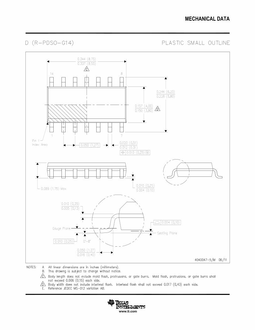
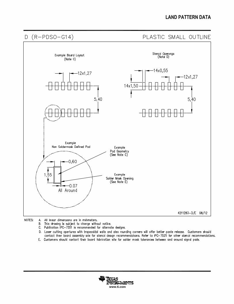


IMPORTANT NOTICE
Texas Instruments Incorporated (TI) reserves the right to make corrections, enhancements, improvements and other changes to itssemiconductor products and services per JESD46, latest issue, and to discontinue any product or service per JESD48, latest issue. Buyersshould obtain the latest relevant information before placing orders and should verify that such information is current and complete.TI’s published terms of sale for semiconductor products (http://www.ti.com/sc/docs/stdterms.htm) apply to the sale of packaged integratedcircuit products that TI has qualified and released to market. Additional terms may apply to the use or sale of other types of TI products andservices.Reproduction of significant portions of TI information in TI data sheets is permissible only if reproduction is without alteration and isaccompanied by all associated warranties, conditions, limitations, and notices. TI is not responsible or liable for such reproduceddocumentation. Information of third parties may be subject to additional restrictions. Resale of TI products or services with statementsdifferent from or beyond the parameters stated by TI for that product or service voids all express and any implied warranties for theassociated TI product or service and is an unfair and deceptive business practice. TI is not responsible or liable for any such statements.Buyers and others who are developing systems that incorporate TI products (collectively, “Designers”) understand and agree that Designersremain responsible for using their independent analysis, evaluation and judgment in designing their applications and that Designers havefull and exclusive responsibility to assure the safety of Designers' applications and compliance of their applications (and of all TI productsused in or for Designers’ applications) with all applicable regulations, laws and other applicable requirements. Designer represents that, withrespect to their applications, Designer has all the necessary expertise to create and implement safeguards that (1) anticipate dangerousconsequences of failures, (2) monitor failures and their consequences, and (3) lessen the likelihood of failures that might cause harm andtake appropriate actions. Designer agrees that prior to using or distributing any applications that include TI products, Designer willthoroughly test such applications and the functionality of such TI products as used in such applications.TI’s provision of technical, application or other design advice, quality characterization, reliability data or other services or information,including, but not limited to, reference designs and materials relating to evaluation modules, (collectively, “TI Resources”) are intended toassist designers who are developing applications that incorporate TI products; by downloading, accessing or using TI Resources in anyway, Designer (individually or, if Designer is acting on behalf of a company, Designer’s company) agrees to use any particular TI Resourcesolely for this purpose and subject to the terms of this Notice.TI’s provision of TI Resources does not expand or otherwise alter TI’s applicable published warranties or warranty disclaimers for TIproducts, and no additional obligations or liabilities arise from TI providing such TI Resources. TI reserves the right to make corrections,enhancements, improvements and other changes to its TI Resources. TI has not conducted any testing other than that specificallydescribed in the published documentation for a particular TI Resource.Designer is authorized to use, copy and modify any individual TI Resource only in connection with the development of applications thatinclude the TI product(s) identified in such TI Resource. NO OTHER LICENSE, EXPRESS OR IMPLIED, BY ESTOPPEL OR OTHERWISETO ANY OTHER TI INTELLECTUAL PROPERTY RIGHT, AND NO LICENSE TO ANY TECHNOLOGY OR INTELLECTUAL PROPERTYRIGHT OF TI OR ANY THIRD PARTY IS GRANTED HEREIN, including but not limited to any patent right, copyright, mask work right, orother intellectual property right relating to any combination, machine, or process in which TI products or services are used. Informationregarding or referencing third-party products or services does not constitute a license to use such products or services, or a warranty orendorsement thereof. Use of TI Resources may require a license from a third party under the patents or other intellectual property of thethird party, or a license from TI under the patents or other intellectual property of TI.TI RESOURCES ARE PROVIDED “AS IS” AND WITH ALL FAULTS. TI DISCLAIMS ALL OTHER WARRANTIES ORREPRESENTATIONS, EXPRESS OR IMPLIED, REGARDING RESOURCES OR USE THEREOF, INCLUDING BUT NOT LIMITED TOACCURACY OR COMPLETENESS, TITLE, ANY EPIDEMIC FAILURE WARRANTY AND ANY IMPLIED WARRANTIES OFMERCHANTABILITY, FITNESS FOR A PARTICULAR PURPOSE, AND NON-INFRINGEMENT OF ANY THIRD PARTY INTELLECTUALPROPERTY RIGHTS. TI SHALL NOT BE LIABLE FOR AND SHALL NOT DEFEND OR INDEMNIFY DESIGNER AGAINST ANY CLAIM,INCLUDING BUT NOT LIMITED TO ANY INFRINGEMENT CLAIM THAT RELATES TO OR IS BASED ON ANY COMBINATION OFPRODUCTS EVEN IF DESCRIBED IN TI RESOURCES OR OTHERWISE. IN NO EVENT SHALL TI BE LIABLE FOR ANY ACTUAL,DIRECT, SPECIAL, COLLATERAL, INDIRECT, PUNITIVE, INCIDENTAL, CONSEQUENTIAL OR EXEMPLARY DAMAGES INCONNECTION WITH OR ARISING OUT OF TI RESOURCES OR USE THEREOF, AND REGARDLESS OF WHETHER TI HAS BEENADVISED OF THE POSSIBILITY OF SUCH DAMAGES.Unless TI has explicitly designated an individual product as meeting the requirements of a particular industry standard (e.g., ISO/TS 16949and ISO 26262), TI is not responsible for any failure to meet such industry standard requirements.Where TI specifically promotes products as facilitating functional safety or as compliant with industry functional safety standards, suchproducts are intended to help enable customers to design and create their own applications that meet applicable functional safety standardsand requirements. Using products in an application does not by itself establish any safety features in the application. Designers mustensure compliance with safety-related requirements and standards applicable to their applications. Designer may not use any TI products inlife-critical medical equipment unless authorized officers of the parties have executed a special contract specifically governing such use.Life-critical medical equipment is medical equipment where failure of such equipment would cause serious bodily injury or death (e.g., lifesupport, pacemakers, defibrillators, heart pumps, neurostimulators, and implantables). Such equipment includes, without limitation, allmedical devices identified by the U.S. Food and Drug Administration as Class III devices and equivalent classifications outside the U.S.TI may expressly designate certain products as completing a particular qualification (e.g., Q100, Military Grade, or Enhanced Product).Designers agree that it has the necessary expertise to select the product with the appropriate qualification designation for their applicationsand that proper product selection is at Designers’ own risk. Designers are solely responsible for compliance with all legal and regulatoryrequirements in connection with such selection.Designer will fully indemnify TI and its representatives against any damages, costs, losses, and/or liabilities arising out of Designer’s non-compliance with the terms and provisions of this Notice.
Mailing Address: Texas Instruments, Post Office Box 655303, Dallas, Texas 75265Copyright © 2017, Texas Instruments Incorporated