ece 260b – cse 241a manufacturing 1 ece260b – cse241a winter 2005 manufacturing website:
TRANSCRIPT

ECE 260B – CSE 241A Manufacturing 1 http://vlsicad.ucsd.edu
ECE260B – CSE241A
Winter 2005
Manufacturing
Website: http://vlsicad.ucsd.edu/courses/ece260b-w05
Slides courtesy of Prof. Andrew B. Kahng
ECE 260B – CSE 241A Manufacturing 2 http://vlsicad.ucsd.edu
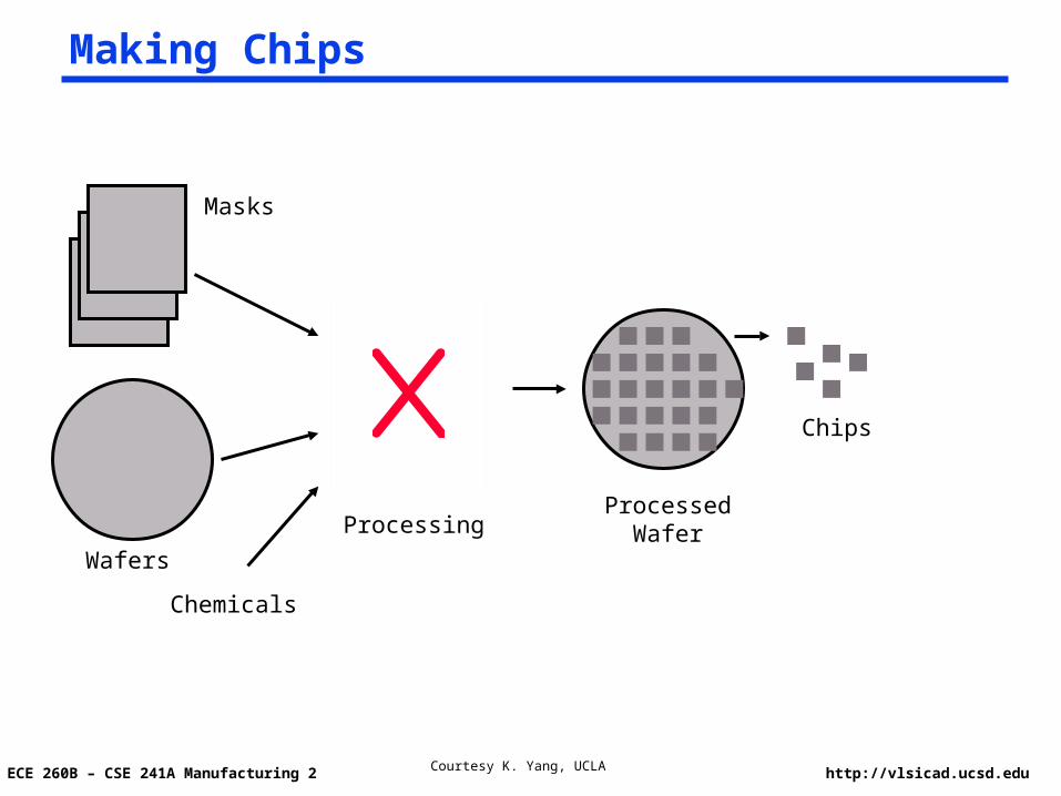
Making Chips
Wafers
Processing
Chemicals
ProcessedWafer
Chips
Masks
Courtesy K. Yang, UCLA

ECE 260B – CSE 241A Manufacturing 3 http://vlsicad.ucsd.edu
Basic Fabrication: Two Steps
(1) Transfer an image of the design to the wafer
(2) Using that image as a guide, create the desired layer on silicon
diffusion (add impurities to the silicon) oxide (create an insulating layer) metal (create a wire layer)
Use the same basic mechanism, photolithography, to do (1)
Use three different methods to do (2) Ion implant - used for diffusion: Shoot impurities at the silicon Deposition - used for oxide/metal: Usually chemical vapor (CVD) Grow - used for some oxides: Place silicon in oxidizing ambient
Courtesy K. Yang, UCLA

ECE 260B – CSE 241A Manufacturing 4 http://vlsicad.ucsd.edu
Photolithography
Repeat: Create a layer on the wafer (either before (oxide, metal) or after
(diffusion) resist) Put a photo-sensitive resist on top of the wafer Optically project an image of the pattern you desire on the wafer Develop the resist Use the resist as a mask to prevent the etch (or other process)
from reaching the layer under the resist, transferring the pattern to the layer
Remove the resist
All die on the wafer are processed in parallel, and for some chemical steps, many wafers are processed in parallel
Courtesy K. Yang, UCLA

ECE 260B – CSE 241A Manufacturing 5 http://vlsicad.ucsd.edu
Photolithography
Start with wafer at current step
Spin on a photoresist
Pattern photoresist with mask
Step specific processingetch, implant, etc...
Wash off resist
Courtesy K. Yang, UCLA

ECE 260B – CSE 241A Manufacturing 6 http://vlsicad.ucsd.edu
Photoresist Types
Positive resists material is removed from
exposed areas during development
most widely used
Negative resists material is removed from
unexposed areas during development
less mature
Mask
Resist
Silicon
Post development profile for positive and negative photoresists

ECE 260B – CSE 241A Manufacturing 7 http://vlsicad.ucsd.edu
Mask Types
Bright field masks opaque features defined by
chrome background is transparent used, e.g., for poly and metal
Dark field masks transparent features defined background is opaque
(chrome) used, e.g., for contacts used also for damascene
metals
Clear areas
Opaque(chrome)
areas

ECE 260B – CSE 241A Manufacturing 8 http://vlsicad.ucsd.edu
Mask (Reticle) Manufacturing
MEBES format and machine, or others
Place a glass plate covered with chrome covered with resist in a high-vacuum column
Use an electron beam spot size smaller than the finest resolution of the design
Scan the surface of the mask with the e-beam in a raster-scan order. Modulate the beam to transfer the pattern to the chrome
Develop the resist, and the chrome, and then remove the resist
Check and correct the chrome pattern
.
.
.
.
All modern processes use masks (reticles) that are 5-10x larger than the desired size. The mask aligners then project the image and reduce it in the projection. While this means that exposing a wafer takes multiple prints, it is needed to reach the resolutions needed for current technologies.
Courtesy K. Yang, UCLA

ECE 260B – CSE 241A Manufacturing 9 http://vlsicad.ucsd.edu
“Yield” in the Semiconductor Industry
Yield : something yielded: PRODUCT; especially: the amount or quantity produced or returned.
Assessment of the quality of the design.
Design for manufacturability (DFM).
Manufacturability : measure of the number of defect-free chips that can be produced from a single wafer[1].
Manufacturability M = Nchip * Y
Cchip = Cwf/(Nchip * Y)
ECE 260B – CSE 241A Manufacturing 10 http://vlsicad.ucsd.edu
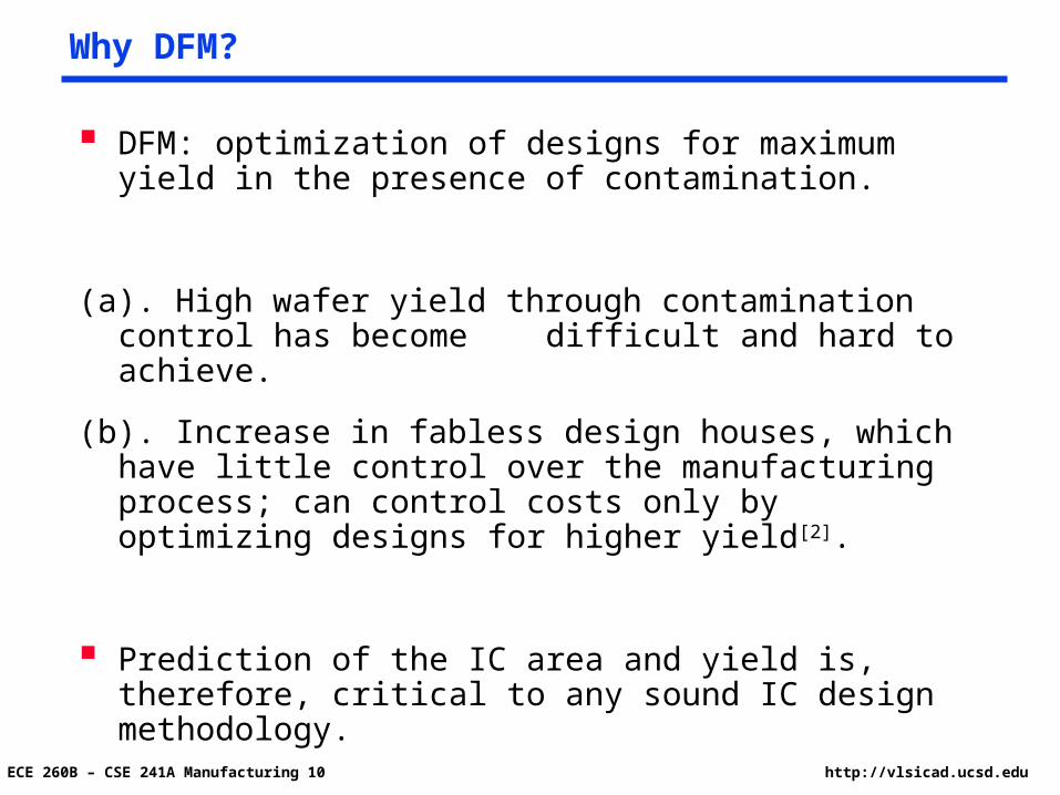
Why DFM?
DFM: optimization of designs for maximum yield in the presence of contamination.
(a). High wafer yield through contamination control has become difficult and hard to achieve.
(b). Increase in fabless design houses, which have little control over the manufacturing process; can control costs only by optimizing designs for higher yield[2].
Prediction of the IC area and yield is, therefore, critical to any sound IC design methodology.

ECE 260B – CSE 241A Manufacturing 11 http://vlsicad.ucsd.edu
Yield Loss in ICs
Yield loss occurs when there is an unacceptable mismatch between the expected and actual parameters of an IC.
Yield loss in ICs are classified into two types:
(a).Functional yield loss (Yfnc) due to spot defects (shorts & opens).
(b).Parametric yield loss (Ypar) due to global process disturbances.
Defects: circular disks of extra/missing material in any layer of the IC[3].
Total Yield = Yfnc * Ypar

ECE 260B – CSE 241A Manufacturing 12 http://vlsicad.ucsd.edu
“Critical Area” in ICs
The susceptibility of an IC layer to a defect is captured by the “critical area” function.
The critical area for a defect of radius rd is defined as that area on a die where if the center of a circular defect falls, a fault occurs in the circuit[3].

ECE 260B – CSE 241A Manufacturing 13 http://vlsicad.ucsd.edu
Interconnect Yield Model
The yield loss primarily takes place in the metals:
(a). The use of the metal layer is more extensive than that of any other layer in the IC.
(b). The defect count is more in the metal layer.
Poisson’s yield model: Y = exp(-A*D);
A = die area; D = defect density.
The interconnect yield Y of the chip[5]:
ACr= critical area; r0 = defect radius; r1 = half (the min. Spacing between metals); K and p are model parameters.

ECE 260B – CSE 241A Manufacturing 14 http://vlsicad.ucsd.edu
Extraction of Critical Area for Shorts
Step 1: Expand each geometry shape by radius R.
Step 2: Find the intersection area of such expanded geometry.
Step 3: Find the union of all intersection area.
Step 4: Repeat steps 1, 2, and 3 for a range of defect sizes[6].

ECE 260B – CSE 241A Manufacturing 15 http://vlsicad.ucsd.edu
Extraction of Critical Area for Opens
Step 1: Shrink both the edges of the conducting path by radius R; extend the left and right edges of the shrunk conducting path by radius R.
Step 2: Shrink all edges of the rectangular contact by radius R.
Step 3: Find the union of the shrunk area.
Step 4: Repeat steps 1, 2, and 3 for a range of defect sizes[4].

ECE 260B – CSE 241A Manufacturing 16 http://vlsicad.ucsd.edu
Critical Area in the IC Layout
ECE 260B – CSE 241A Manufacturing 17 http://vlsicad.ucsd.edu
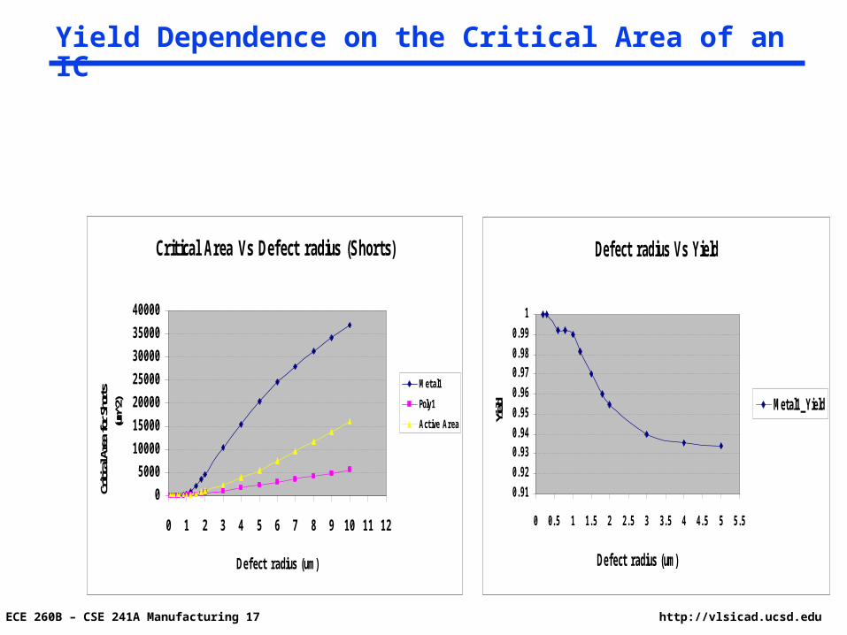
Yield Dependence on the Critical Area of an IC
Critical Area Vs Defect radius (Shorts)
0
5000
10000
15000
20000
25000
30000
35000
40000
0 1 2 3 4 5 6 7 8 9 10 11 12
Defect radius (um)
Criti
cal A
rea
for S
hort
s (um̂
2)
Metal1
Poly1
Active Area
Defect radius Vs Yield
0.91
0.92
0.930.94
0.95
0.96
0.970.98
0.99
1
0 0.5 1 1.5 2 2.5 3 3.5 4 4.5 5 5.5
Defect radius (um)
Yield Metal1_Yield

ECE 260B – CSE 241A Manufacturing 18 http://vlsicad.ucsd.edu
Yield Enhancement by Layout Optimization
Design of appropriate cells, that are small in size.
Choosing smart place and route strategies/optimization of wire spacing.
(a). Additional Interconnect layers.
(b). Reducing Cell Utilization.
(c). Relaxing metal design rules[7].

ECE 260B – CSE 241A Manufacturing 19 http://vlsicad.ucsd.edu
OPC and PSM
ECE 260B – CSE 241A Manufacturing 20 http://vlsicad.ucsd.edu
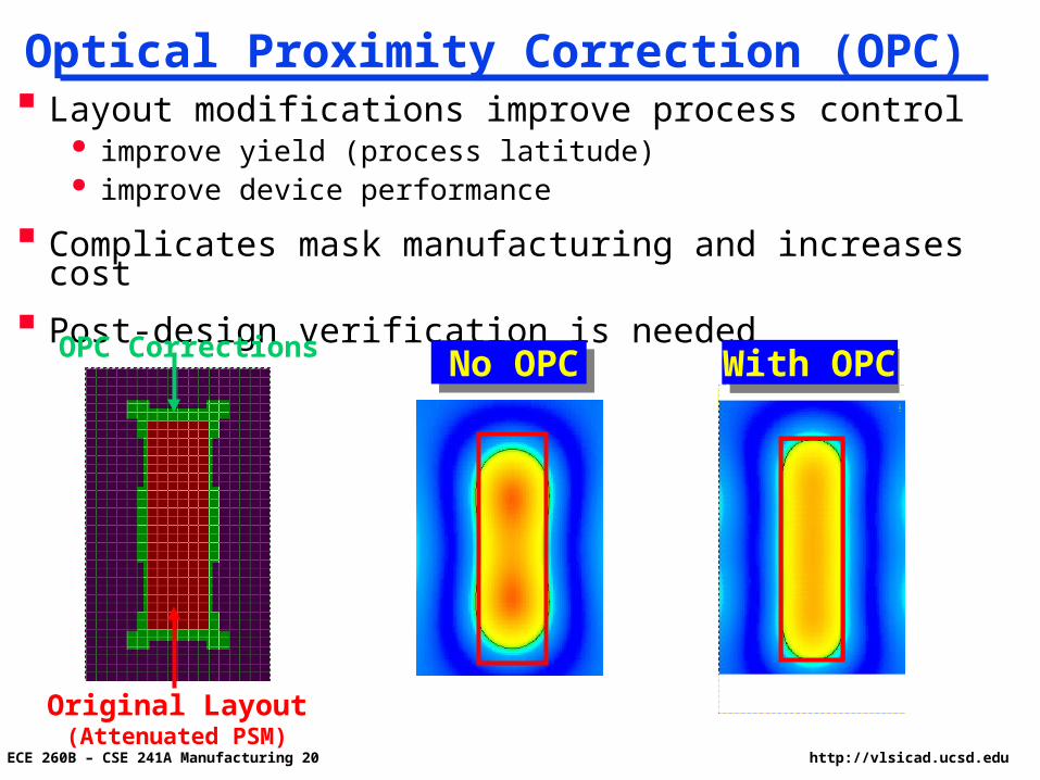
Optical Proximity Correction (OPC) Layout modifications improve process control
improve yield (process latitude) improve device performance
Complicates mask manufacturing and increases cost
Post-design verification is needed
With OPCNo OPC
Original Layout(Attenuated PSM)
OPC Corrections

ECE 260B – CSE 241A Manufacturing 21 http://vlsicad.ucsd.edu
OPC Mechanisms
Serifs: corner rounding
Hammerheads: line-end shortening
Gate assists (subresolution
scattering bars): CD control
Gate biasing: CD control
Affects custom,
hierarchical and
reuse-based layout
methodologies

ECE 260B – CSE 241A Manufacturing 22 http://vlsicad.ucsd.edu
Rule-Based OPC vs. Model-Based OPC
Rule-Based OPC Apply corrections based on a set of predetermined rules
Fast design time, lower mask complexity
Suitable for less aggressive designs
Model-Based OPC Use process simulation to determine corrections on-line
Longer design time, increased mask complexity
Suitable for aggressive designs
ECE 260B – CSE 241A Manufacturing 23 http://vlsicad.ucsd.edu
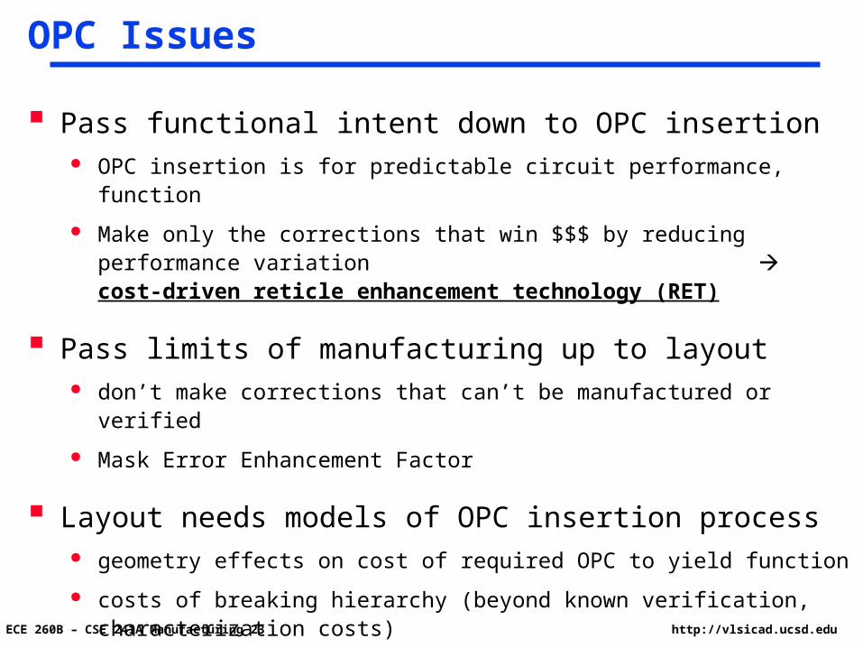
OPC Issues
Pass functional intent down to OPC insertion OPC insertion is for predictable circuit performance, function
Make only the corrections that win $$$ by reducing performance variation cost-driven reticle enhancement technology (RET)
Pass limits of manufacturing up to layout don’t make corrections that can’t be manufactured or verified
Mask Error Enhancement Factor
Layout needs models of OPC insertion process geometry effects on cost of required OPC to yield function
costs of breaking hierarchy (beyond known verification, characterization costs)

ECE 260B – CSE 241A Manufacturing 24 http://vlsicad.ucsd.edu
Mask Costs(1)
Design Mask
OPC Fracture
Mask Cost Data Volume
OPC, PSM, Fill increased feature complexity increased mask cost
Figure courtesy Synopsys Inc.

ECE 260B – CSE 241A Manufacturing 25 http://vlsicad.ucsd.edu
Context dependence: Same pattern, different fracture
P. Buck, Dupont Photomasks – ISMT Mask-EDA Workshop July 2001
$1M NRE: Mask Write and Inspection Times$1M NRE: Mask Write and Inspection Times
ECE 260B – CSE 241A Manufacturing 26 http://vlsicad.ucsd.edu
$1M NRE: Mask Write and Inspection Times$1M NRE: Mask Write and Inspection Times
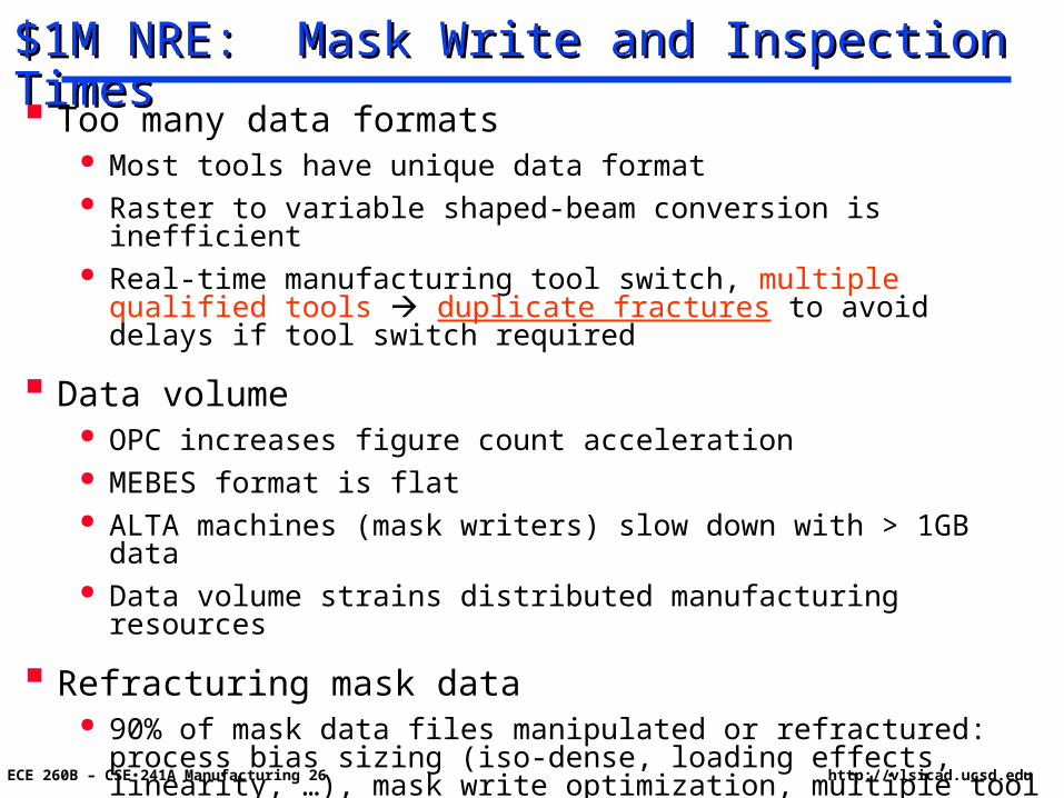
Too many data formats Most tools have unique data format Raster to variable shaped-beam conversion is inefficient Real-time manufacturing tool switch, multiple qualified tools
duplicate fractures to avoid delays if tool switch required
Data volume OPC increases figure count acceleration MEBES format is flat ALTA machines (mask writers) slow down with > 1GB data Data volume strains distributed manufacturing resources
Refracturing mask data 90% of mask data files manipulated or refractured: process bias sizing
(iso-dense, loading effects, linearity, …), mask write optimization, multiple tool formats, …

ECE 260B – CSE 241A Manufacturing 27 http://vlsicad.ucsd.edu
ME
BE
S D
ata
Vo
lum
e (G
B)
Year
P. Buck, Dupont Photomasks – ISMT Mask-EDA Workshop July 2001
ITRS Maximum Single Layer File Size

ECE 260B – CSE 241A Manufacturing 28 http://vlsicad.ucsd.edu
ABF Data Volume (MB)
Wri
te T
ime
(Ref
or m
at +
Pri
nt)
(H
rs)
P. Buck, Dupont Photomasks – ISMT Mask-EDA Workshop July 2001
Mask Write Time vs. Data Volume

ECE 260B – CSE 241A Manufacturing 29 http://vlsicad.ucsd.edu
Fracturing Problem
Mask Data Process Flow
Layout Extraction
RET
Circuit Design
Tape OutJob Decomposition
Mask Data Preparation
Mask Making
Writing
Inspection
Metrology
Tonality
PEC Fracturing
Job Finishing
Fracturing

ECE 260B – CSE 241A Manufacturing 30 http://vlsicad.ucsd.edu
Challenges in Fracturing
• A shot whose minimum width < is called a sliver
<
sliverslant
• # shots increase mask writing time increase cost increase
• each shot should be an axis-parallel trapezoid• the side size of each shot < M
• slant edges should not be partitioned
• # slivers increase mask error enhancement factor (MEEF) increaselarger CD variation and error yield decrease

ECE 260B – CSE 241A Manufacturing 31 http://vlsicad.ucsd.edu
Fracturing Problem
a list of polygons P with axis parallel and slant edges
Max shot size M
Slivering size
Partition P into non-overlapping trapezoidal shots
Number of shots and number of slivers
Given:
Minimizing:
Normal fracturing Reverse tone fracturing

ECE 260B – CSE 241A Manufacturing 32 http://vlsicad.ucsd.edu
A “Ray Selection” Problem
Two candidates to kill one concave point
• For each concave point (include inner point), choose one out of two candidate rays to minimize # slivers
They are called as “conflict pair”
ECE 260B – CSE 241A Manufacturing 33 http://vlsicad.ucsd.edu
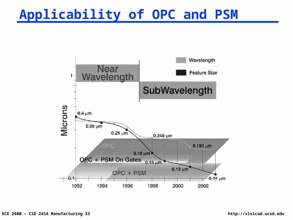
Applicability of OPC and PSM

ECE 260B – CSE 241A Manufacturing 34 http://vlsicad.ucsd.edu
Mask NRE Cost (SEMATECH, 1999)
“$1M mask set” at 100nm, but average only 500 wafers per set

ECE 260B – CSE 241A Manufacturing 35 http://vlsicad.ucsd.edu
The light interacting with the mask is a wave
Any wave has certain fundamental properties Wavelength () Direction Amplitude Phase
RET is wavefront engineering to enhance lithographyby controlling these properties
RET Basics
-4
-3
-2
-1
0
1
2
3
4
-20 0 20 40 60 80 100
B
Amplitude
Direction
Phase
Courtesy F. Schellenberg, Mentor Graphics Corp.
ECE 260B – CSE 241A Manufacturing 36 http://vlsicad.ucsd.edu
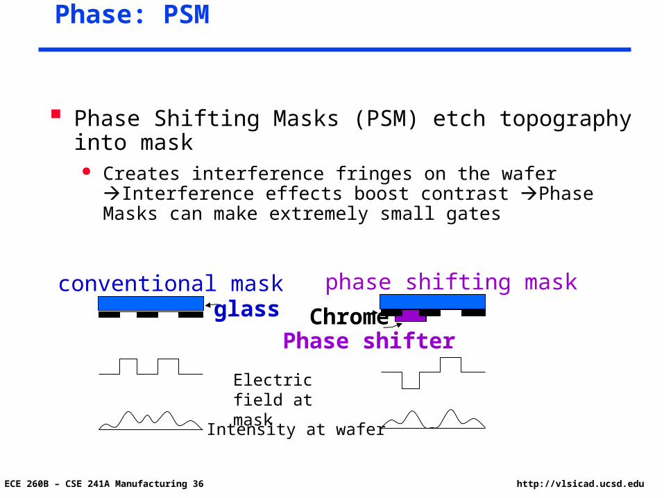
Phase: PSM
Phase Shifting Masks (PSM) etch topography into mask Creates interference fringes on the wafer Interference effects
boost contrast Phase Masks can make extremely small gates
conventional maskglass Chrome
Electric field at mask
Intensity at wafer
phase shifting mask
Phase shifter

ECE 260B – CSE 241A Manufacturing 37 http://vlsicad.ucsd.edu
Forms of Bright-Field Alternating PSM
Single exposure phase transitions required, e.g., 0-60-120-180
or 90-0-270 to avoid printing phase edges throughput unaffected limited improvement in process latitude mask manufacturing difficult, mask cost very high
Double exposure PSM with 0 and 180 degree phase shifters define only critical features ("locally bright-field"), rest of mask is
chrome second exposure with clear-field binary mask protects critical
features, defines non-critical features as well better process latitude decrease in throughput (double exposure)
90° 270° 180°
60°
120°
0°

ECE 260B – CSE 241A Manufacturing 38 http://vlsicad.ucsd.edu
Double-Exposure Bright-Field PSM
0
180180 + =

ECE 260B – CSE 241A Manufacturing 39 http://vlsicad.ucsd.edu
Gate Shrink
ECE 260B – CSE 241A Manufacturing 40 http://vlsicad.ucsd.edu
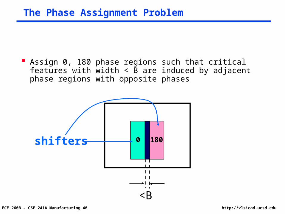
The Phase Assignment Problem
Assign 0, 180 phase regions such that critical features with width < B are induced by adjacent phase regions with opposite phases
0 180
<B
shifters

ECE 260B – CSE 241A Manufacturing 41 http://vlsicad.ucsd.edu
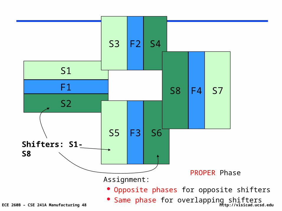
Phase Assignment for Bright-Field PSM
PROPER Phase Assignment: Opposite phases for opposite shifters Same phase for overlapping shifters
Overlapping shifters

ECE 260B – CSE 241A Manufacturing 42 http://vlsicad.ucsd.edu
Key: Global 2-Colorability
?180 0
0180 180
180
Odd cycle of “phase implications” layout cannot be manufactured
layout verification becomes a global, not local, issue

ECE 260B – CSE 241A Manufacturing 43 http://vlsicad.ucsd.edu
Phase Conflict and the Conflict Graph
Self-consistent phase assignment is not possible if there is an odd cycle in the conflict graph
Phase-assignable = conflict graph is bipartite = no odd cycles
this is a global issue! features on one side of chip can affect features on the
other side
Breaking odd cycles: must change the layout! change feature dimensions, and/or change spacings Many degrees of freedom, e.g., layer reassignment for
interconnects

ECE 260B – CSE 241A Manufacturing 44 http://vlsicad.ucsd.edu
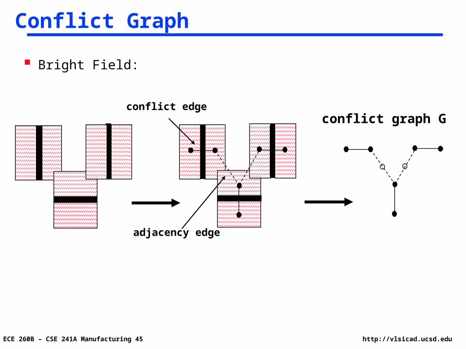
Conflict Graph
Bright Field: build graph over shifter regions shifters for features whose width is < B two edge types adjacency edge between overlapping phase regions :
endpoints must have same phase conflict edge between shifters on opposite side of critical
feature: endpoints must have opposite phase
ECE 260B – CSE 241A Manufacturing 45 http://vlsicad.ucsd.edu
Conflict Graph
Bright Field:
conflict edge
adjacency edge
conflict graph G

ECE 260B – CSE 241A Manufacturing 46 http://vlsicad.ucsd.edu
F4
F2
F3
F1
Critical features: F1,F2,F3,F4

ECE 260B – CSE 241A Manufacturing 47 http://vlsicad.ucsd.edu
F4
F2
F3
F1
Opposite-Phase Shifters (0,180)
ECE 260B – CSE 241A Manufacturing 48 http://vlsicad.ucsd.edu
F4
F2
F3
F1
S1
S2
S3
S5
S4
S6
S7S8
Shifters: S1-S8
PROPER Phase Assignment: Opposite phases for opposite shifters Same phase for overlapping shifters

ECE 260B – CSE 241A Manufacturing 49 http://vlsicad.ucsd.edu
F4
F2
F3
F1
S1
S2
S3
S5
S4
S6
S7S8
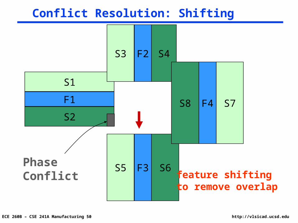
Phase Conflict
Proper Phase Assignment is IMPOSSIBLE
Phase Conflict
ECE 260B – CSE 241A Manufacturing 50 http://vlsicad.ucsd.edu
F4
F2
F3
F1
S1
S2
S3
S5
S4
S6
S7S8
Phase Conflictfeature shiftingto remove overlap
Conflict Resolution: Shifting

ECE 260B – CSE 241A Manufacturing 51 http://vlsicad.ucsd.edu
F4
F2
F1
S1
S2
S3 S4
S7S8
Phase Conflictfeature widening to turnconflict into non-conflict
Conflict Resolution: Widening
F3

ECE 260B – CSE 241A Manufacturing 52 http://vlsicad.ucsd.edu
Minimum Perturbation Problem
Layout modifications feature shifting feature widening
area increase, slowing down
manual fixing, design cost increase
Minimum Perturbation Problem: Find min # of layout modifications leading to proper phase assignment. [Kahng et al. ASPDAC 2001]

ECE 260B – CSE 241A Manufacturing 53 http://vlsicad.ucsd.edu
PSM = Whose Problem?
Must partition responsibility for phase-assignability into at least three domains
Good layout practices No T’s, no doglegs, even-length fingers on transistors, … Open problem: What “design rules” guarantee phase-assignability
without too much loss of density?
Automatic phase conflict resolution
Reuse of pre-existing layout E.g., the entire standard-cell methodology is based on the
assumption of “free composability” of cells within rows (as long as the cells don’t overlap)
Open problem: How to phase-assign layouts, such that no odd cycles of conflict occur when the layouts are composed

ECE 260B – CSE 241A Manufacturing 54 http://vlsicad.ucsd.edu
Conflict Graph for Cell-Based Layouts
Coarse view: at level of connected components of conflict graphs within each cell master
- each of these components is independently phase-assignable
- can be treated as a single “vertex” in coarse-grain conflict graph
edge in coarse-grain conflict graph
cell master A cell master Bconnected component

ECE 260B – CSE 241A Manufacturing 55 http://vlsicad.ucsd.edu
“Compaction-Based” PSM Layout Flow
Analyze input layout
Find min-cost set of perturbations needed to eliminate all “odd cycles”
Induce shape, spacing constraints for new output layout
“Compact” to get phase-assignable layout
Goal: Minimize the set of new constraints, i.e., break all odd cycles in conflict graph by deleting a minimum number of edges

ECE 260B – CSE 241A Manufacturing 56 http://vlsicad.ucsd.edu
Conflict Edge Weight
Which conflict edges are cheapest to break?
Critical paths (e.g., in compactor) in x- and y-directions define layout area
Conflict edges not on critical path: break for free Criticality: with respect to, e.g., area or timing
critical path

ECE 260B – CSE 241A Manufacturing 57 http://vlsicad.ucsd.edu
Density Control for CMP

ECE 260B – CSE 241A Manufacturing 58 http://vlsicad.ucsd.edu
Damascene and Dual-Damascene Process Damascene process named after the ancient Middle Eastern
technique for inlaying metal in ceramic or wood for decoration
• Single Damascene • Dual Damascene
ILD Deposition
Oxide Trench Etch
Metal Fill
Metal CMP
Oxide Trench / Via Etch
Metal Fill
Metal CMP

ECE 260B – CSE 241A Manufacturing 59 http://vlsicad.ucsd.edu
Layout Density Control Flow
Density Analysis• find total feature area in each window• find maximum/minimum total feature area over all w w windows
Fill synthesis• compute amounts, locations of dummy fill• generate fill geometries
• find slack (available area for filling) in each window

ECE 260B – CSE 241A Manufacturing 60 http://vlsicad.ucsd.edu
Fixed r-Dissection Regime
Feature area density bounds enforced only for fixed set of w w windows
Layout partitioned by r2 distinct fixed dissections
Each w w window is partitioned in r2 tiles
How different is this from the regime of “continuous” window locations?
tile
overlapping windows
fixed r-dissectionwith r = 4

ECE 260B – CSE 241A Manufacturing 61 http://vlsicad.ucsd.edu
Filling Problem
ECE 260B – CSE 241A Manufacturing 62 http://vlsicad.ucsd.edu
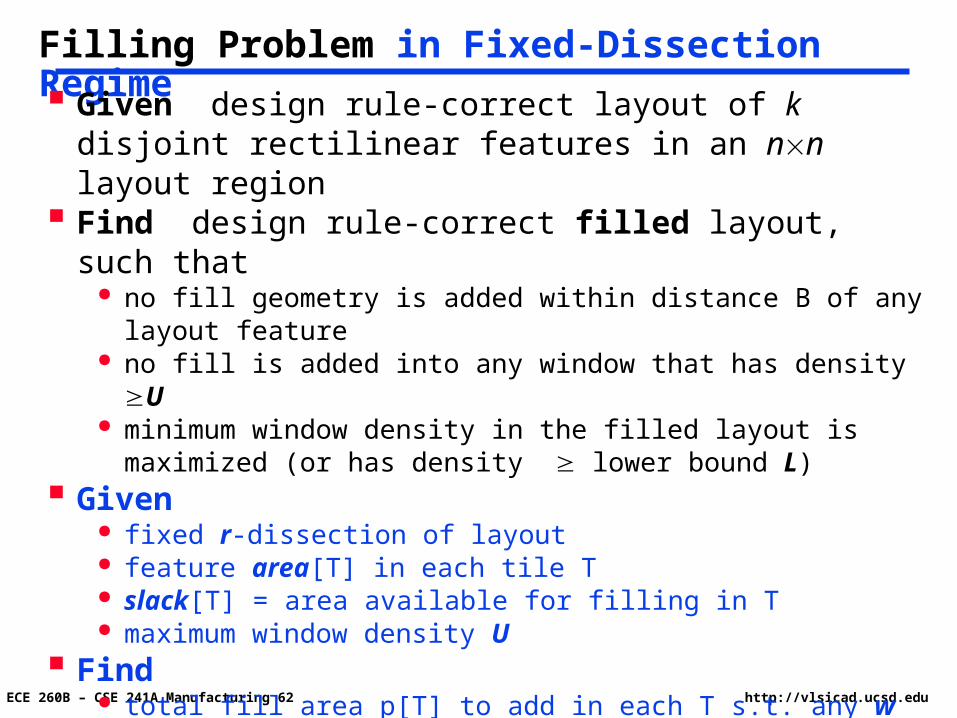
Filling Problem in Fixed-Dissection Regime
Given design rule-correct layout of k disjoint rectilinear features in an nn layout region
Find design rule-correct filled layout, such that no fill geometry is added within distance B of any layout feature no fill is added into any window that has density U minimum window density in the filled layout is maximized (or has
density lower bound L) Given
fixed r-dissection of layout feature area[T] in each tile T slack[T] = area available for filling in T maximum window density U
Find total fill area p[T] to add in each T s.t. any w w window W has
density U minW T W (area[T] + p[T]) is maximized
ECE 260B – CSE 241A Manufacturing 63 http://vlsicad.ucsd.edu
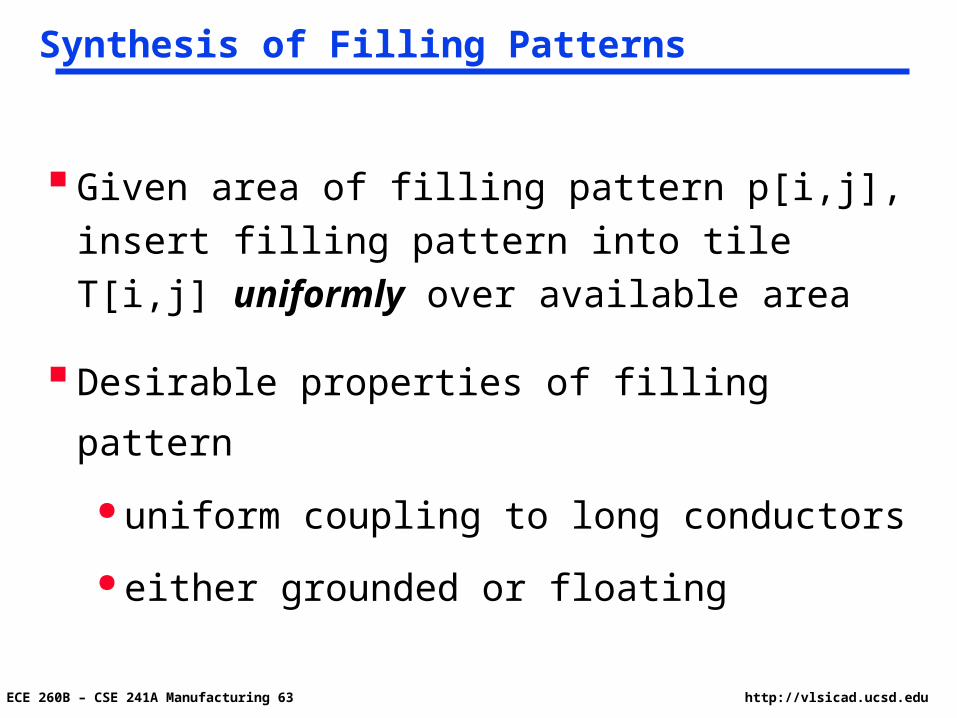
Synthesis of Filling Patterns
Given area of filling pattern p[i,j], insert filling
pattern into tile T[i,j] uniformly over available area
Desirable properties of filling pattern
uniform coupling to long conductors
either grounded or floating

ECE 260B – CSE 241A Manufacturing 64 http://vlsicad.ucsd.edu
Basket-Weave Fill Pattern
Each vertical/horizontal crossover line has same overlap capacitance to fill

ECE 260B – CSE 241A Manufacturing 65 http://vlsicad.ucsd.edu
Grounded Fill Pattern
Fill with horizontal stripes,
then span with vertical lines

ECE 260B – CSE 241A Manufacturing 66 http://vlsicad.ucsd.edu
Flow Implications
Accurate estimation of filling is needed in PD, PV tools (else broken performance analysis flow)
Filling geometries affect capacitance extraction by > 50%
Multilayer problem (coupling to critical nets, contacting restrictions, active layers, other interlayer dependencies)

ECE 260B – CSE 241A Manufacturing 67 http://vlsicad.ucsd.edu
Issues With Current Tools
Only the average overall feature density is constrained, while local variation in feature density is ignored
Density analysis does not find true extremal window densities - instead, it finds extremal window densities only over fixed set of window positions
Fill insertion into layout does not minimize the maximum variation in window density
In part, due to physical verification tool heritage Boolean operations Never empowered to change the layout

ECE 260B – CSE 241A Manufacturing 68 http://vlsicad.ucsd.edu
Len Aberration
Cell A
Cell A
Cell A
(X 1 , Y 1)
(X 0 , Y 0)
(X 2 , Y 2)
F ie ld-dependentaberrationsaffect the fide lityand p lacem entof critica l c ircu itfeatures.
Big C hip
Example: Field-dependent aberrations cause placement errors and distortions ( location-specific cell variants?)
),(A_CELL),(A_CELL),(A_CELL 220011 YXYXYX
Center: Minimal Aberrations
Edge: High Aberrations
Tow
ard
s Le
ns
Wafer Plane
Lens
R. Pack, Cadence

ECE 260B – CSE 241A Manufacturing 69 http://vlsicad.ucsd.edu
ThanksThanks