ee 584 introduction to vlsi design and testing
TRANSCRIPT
1
EE 584 INTRODUCTION TO VLSI DESIGN AND TESTING
INVERTER FANOUT 3 RINGOSCILLATOR
Group 11 members
1. CAVATURU
2. GUDURU
3. MADDURI
4. VANKADARA

2
Table of contents
1. Goal of the project……………………………………………………………….3
2. Introduction………………………………………………………………………3
3. Input buffer………………………………………………………………………4
4. Ring oscillator……………………………………………………………………9
5. output buffer…………………………………………………………………….15
6. divide by 4 circuit……………………………………………………………….19
7. corner process…………………………………………………………………...23
3
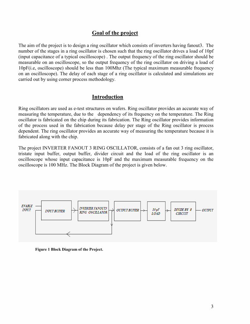
Goal of the project
The aim of the project is to design a ring oscillator which consists of inverters having fanout3. The
number of the stages in a ring oscillator is chosen such that the ring oscillator drives a load of 10pf
(input capacitance of a typical oscilloscope) . The output frequency of the ring oscillator should be
measurable on an oscilloscope, so the output frequency of the ring oscillator on driving a load of
10pF(i.e, oscilloscope) should be less than 100Mhz (The typical maximum measurable frequency
on an oscilloscope). The delay of each stage of a ring oscillator is calculated and simulations are
carried out by using corner process methodology.
Introduction
Ring oscillators are used as e-test structures on wafers. Ring oscillator provides an accurate way of
measuring the temperature, due to the dependency of its frequency on the temperature. The Ring
oscillator is fabricated on the chip during its fabrication. The Ring oscillator provides information
of the process used in the fabrication because delay per stage of the Ring oscillator is process
dependent. The ring oscillator provides an accurate way of measuring the temperature because it is
fabricated along with the chip.
The project INVERTER FANOUT 3 RING OSCILLATOR, consists of a fan out 3 ring oscillator,
tristate input buffer, output buffer, divider circuit and the load of the ring oscillator is an
oscilloscope whose input capacitance is 10pF and the maximum measurable frequency on the
oscilloscope is 100 MHz. The Block Diagram of the project is given below.
Figure 1 Block Diagram of the Project.
4
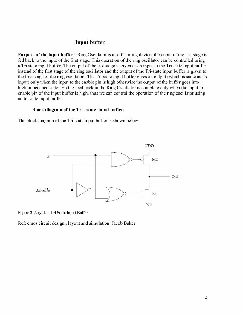
Input buffer
Purpose of the input buffer: Ring Oscillator is a self starting device, the ouput of the last stage is
fed back to the input of the first stage. This operation of the ring oscillator can be controlled using
a Tri state input buffer. The output of the last stage is given as an input to the Tri-state input buffer
instead of the first stage of the ring oscillator and the output of the Tri-state input buffer is given to
the first stage of the ring oscillator . The Tri-state input buffer gives an output (which is same as its
input) only when the input to the enable pin is high otherwise the output of the buffer goes into
high impedance state . So the feed back in the Ring Oscillator is complete only when the input to
enable pin of the input buffer is high, thus we can control the operation of the ring oscillator using
an tri-state input buffer.
Block diagram of the Tri –state input buffer:
The block diagram of the Tri-state input buffer is shown below
Figure 2 A typical Tri State Input Buffer
Ref: cmos circuit design , layout and simulation ,Jacob Baker
5
Schematic of the input buffer: The schematic of the input buffer is shown in the figure. The W/L
ratios of nand and nor are chosen such that both will have equal rise time and fall time.
Figure 3 Input Buffer Schematic.
6
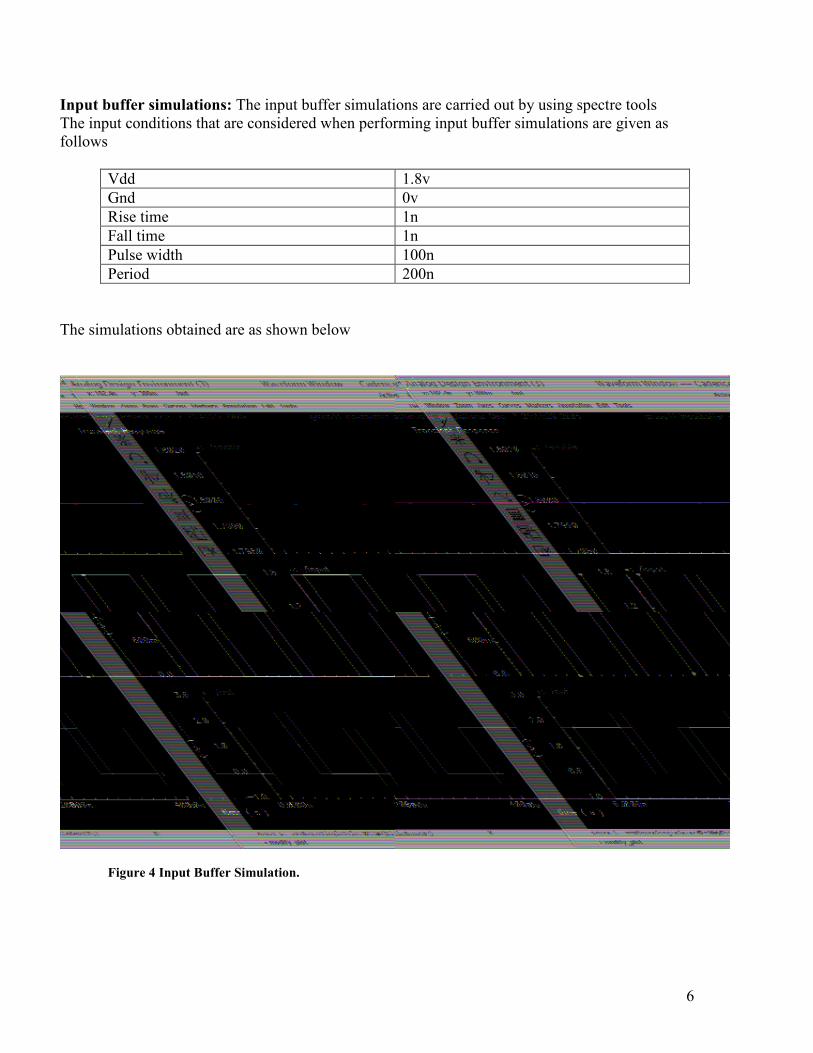
Input buffer simulations: The input buffer simulations are carried out by using spectre tools
The input conditions that are considered when performing input buffer simulations are given as
follows
Vdd 1.8v
Gnd 0v
Rise time 1n
Fall time 1n
Pulse width 100n
Period 200n
The simulations obtained are as shown below
Figure 4 Input Buffer Simulation.
7
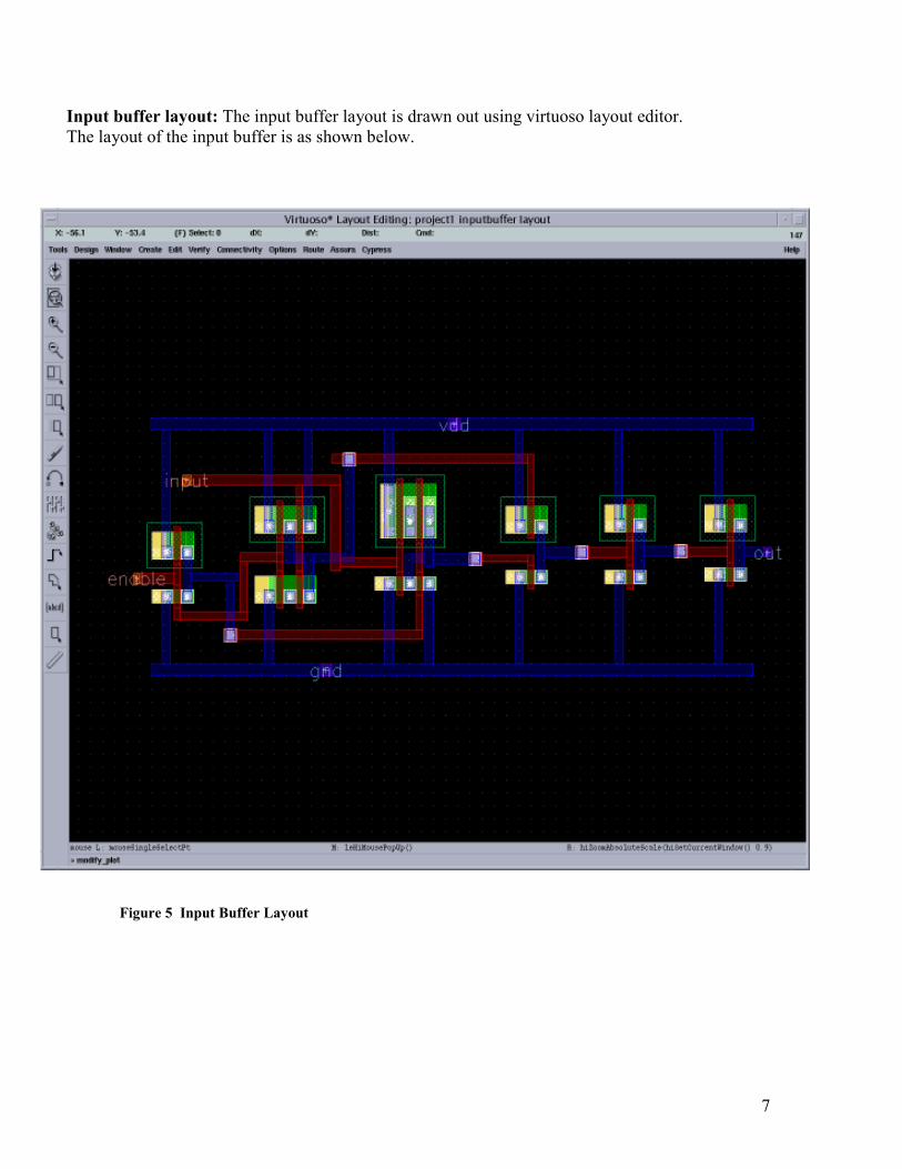
Input buffer layout: The input buffer layout is drawn out using virtuoso layout editor.
The layout of the input buffer is as shown below.
Figure 5 Input Buffer Layout
8
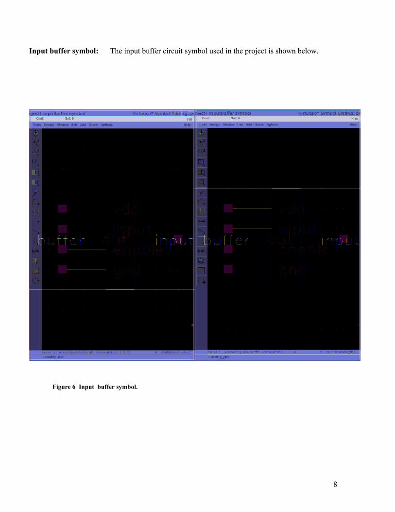
Input buffer symbol: The input buffer circuit symbol used in the project is shown below.
Figure 6 Input buffer symbol.

9
RING OSCILLATOR
Description: A ring oscillator consists of odd number of inverters in which the output of the last
inverter is fed to the input of the first inverter. The frequency of the ring oscillator is calculated by
the formula
F = 1/N (Tphl+Tplh)
Where
N: odd number of the stages in the ring oscillator
Tphl: Time taken for low to high transition
Tplh: Time taken for high to low transition
F: Frequency of the ring oscillator
Ref: CMOS circuit design and layout 2nd edition, Baker
Thus, ring oscillator frequency depends upon the number of stages.
10
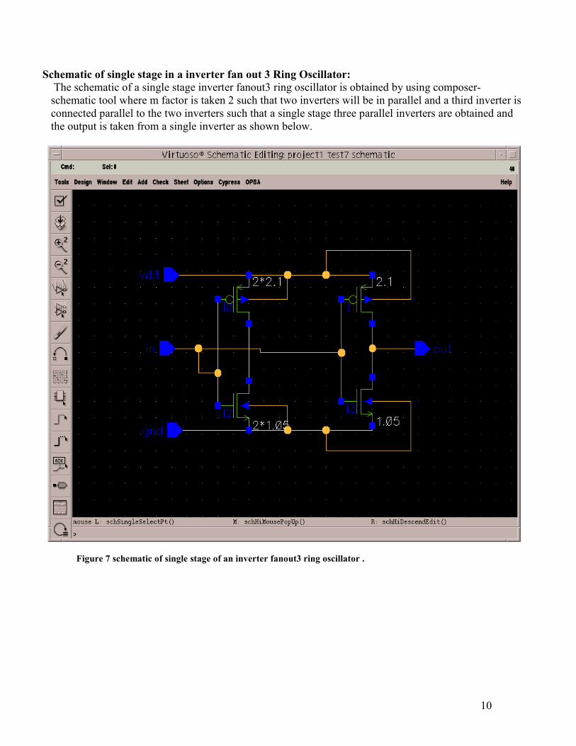
Schematic of single stage in a inverter fan out 3 Ring Oscillator:
The schematic of a single stage inverter fanout3 ring oscillator is obtained by using composer-
schematic tool where m factor is taken 2 such that two inverters will be in parallel and a third inverter is
connected parallel to the two inverters such that a single stage three parallel inverters are obtained and
the output is taken from a single inverter as shown below.
Figure 7 schematic of single stage of an inverter fanout3 ring oscillator .
11
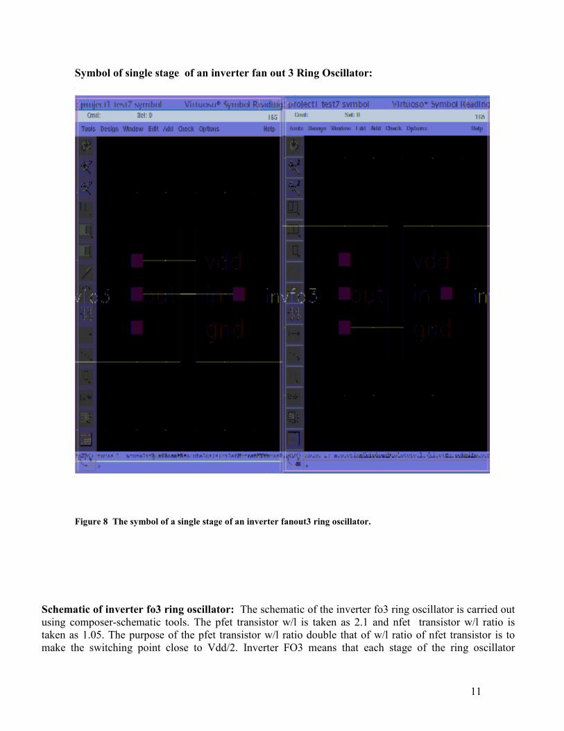
Symbol of single stage of an inverter fan out 3 Ring Oscillator:
g
Figure 8 The symbol of a single stage of an inverter fanout3 ring oscillator.
Schematic of inverter fo3 ring oscillator: The schematic of the inverter fo3 ring oscillator is carried out
using composer-schematic tools. The pfet transistor w/l is taken as 2.1 and nfet transistor w/l ratio is
taken as 1.05. The purpose of the pfet transistor w/l ratio double that of w/l ratio of nfet transistor is to
make the switching point close to Vdd/2. Inverter FO3 means that each stage of the ring oscillator
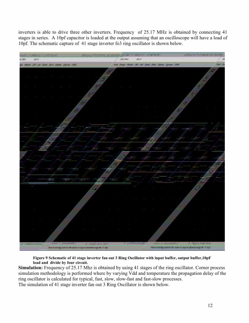
12
inverters is able to drive three other inverters. Frequency of 25.17 MHz is obtained by connecting 41
stages in series. A 10pf capacitor is loaded at the output assuming that an oscilloscope will have a load of
10pf. The schematic capture of 41 stage inverter fo3 ring oscillator is shown below.
Figure 9 Schematic of 41 stage inverter fan out 3 Ring Oscillator with input buffer, output buffer,10pF
load and divide by four circuit.
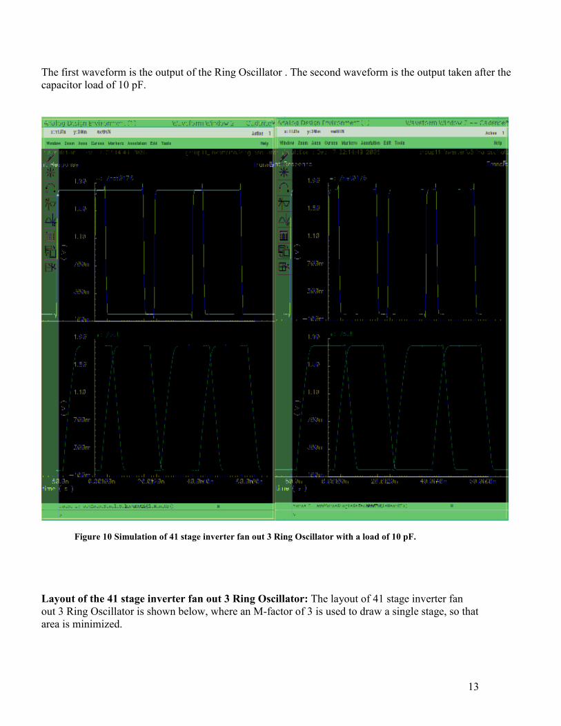
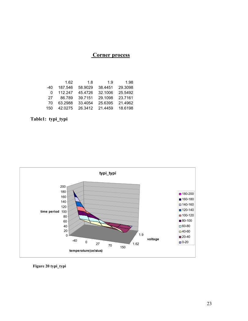
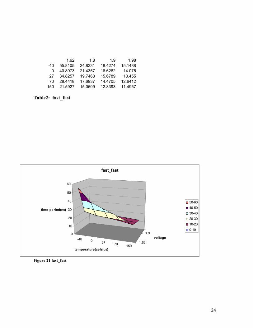
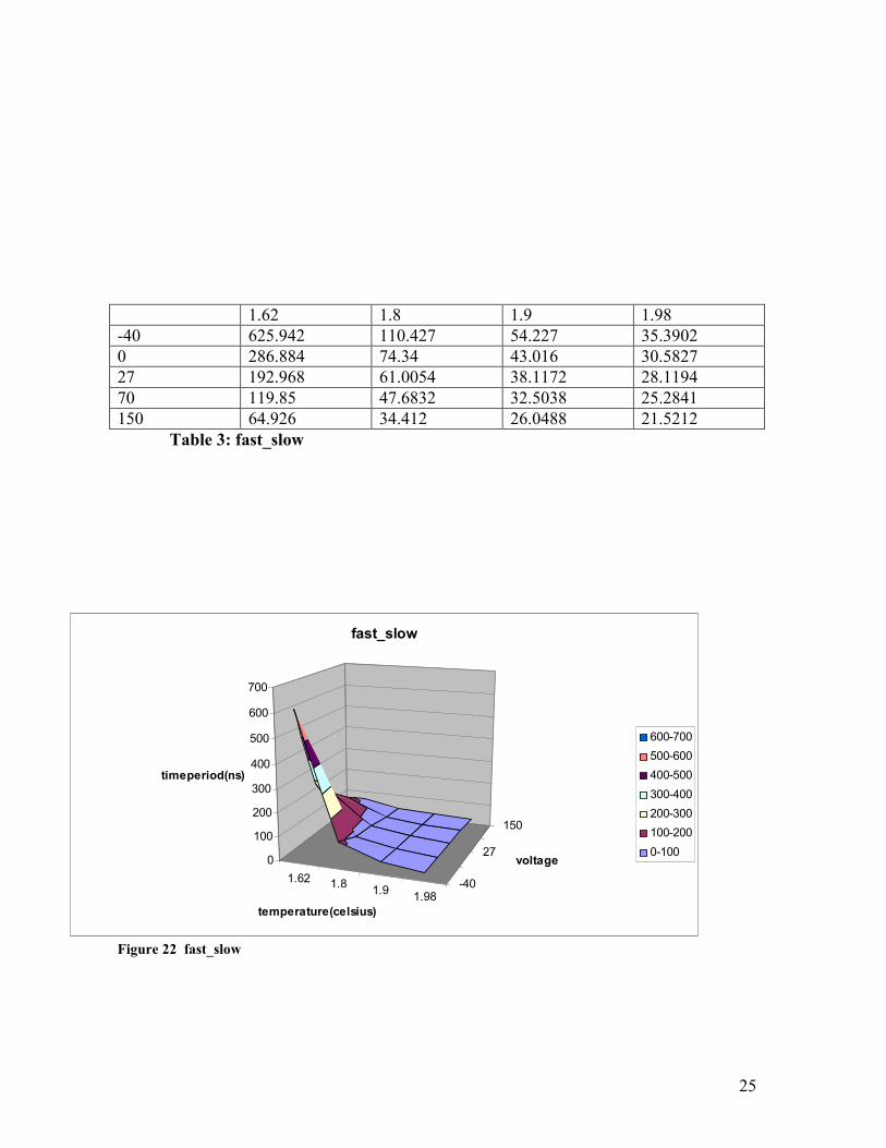
Simulation: Frequency of 25.17 Mhz is obtained by using 41 stages of the ring oscillator. Corner process
simulation methodology is performed where by varying Vdd and temperature the propagation delay of the
ring oscillator is calculated for typical, fast, slow, slow-fast and fast-slow processes.
The simulation of 41 stage inverter fan out 3 Ring Oscillator is shown below.
13
The first waveform is the output of the Ring Oscillator . The second waveform is the output taken after the
capacitor load of 10 pF.
Figure 10 Simulation of 41 stage inverter fan out 3 Ring Oscillator with a load of 10 pF.
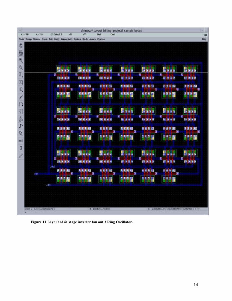
Layout of the 41 stage inverter fan out 3 Ring Oscillator: The layout of 41 stage inverter fan
out 3 Ring Oscillator is shown below, where an M-factor of 3 is used to draw a single stage, so that
area is minimized.
14
Figure 11 Layout of 41 stage inverter fan out 3 Ring Oscillator.
15
Output buffer
Purpose of the output buffer: The frequency of the Ring Oscillator is calculated using an
oscilloscope. The oscilloscope capacitance is estimated as 10Pf. So in order to drive such a heavy
load of 10pF output buffer is needed.
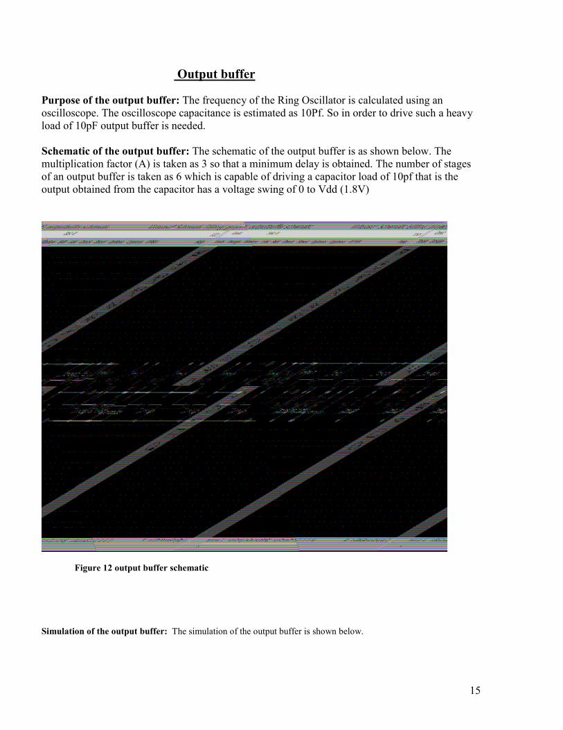
Schematic of the output buffer: The schematic of the output buffer is as shown below. The
multiplication factor (A) is taken as 3 so that a minimum delay is obtained. The number of stages
of an output buffer is taken as 6 which is capable of driving a capacitor load of 10pf that is the
output obtained from the capacitor has a voltage swing of 0 to Vdd (1.8V)
Figure 12 output buffer schematic
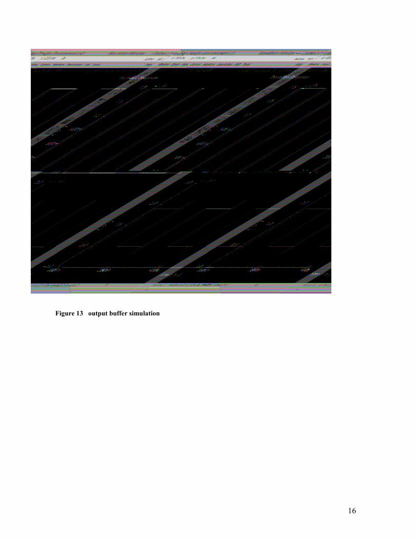
Simulation of the output buffer: The simulation of the output buffer is shown below.
16
Figure 13 output buffer simulation
17
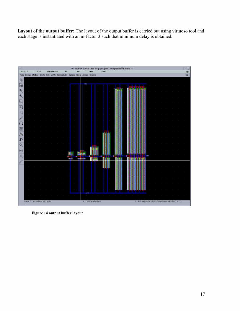
Layout of the output buffer: The layout of the output buffer is carried out using virtuoso tool and
each stage is instantiated with an m-factor 3 such that minimum delay is obtained.
Figure 14 output buffer layout
18
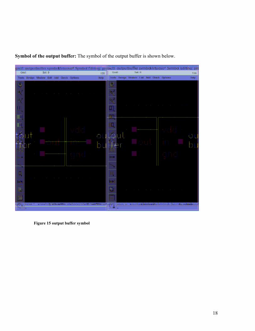
Symbol of the output buffer: The symbol of the output buffer is shown below.
Figure 15 output buffer symbol
19
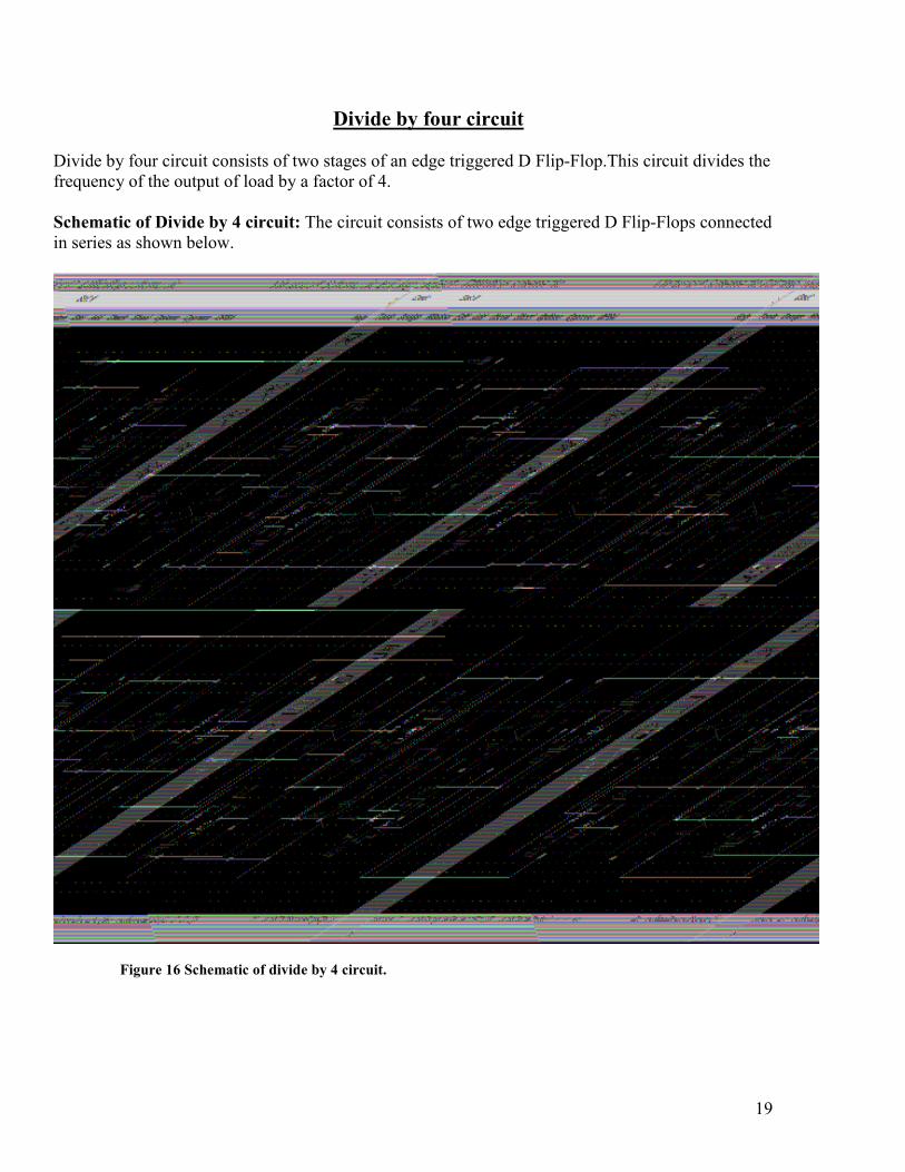
Divide by four circuit
Divide by four circuit consists of two stages of an edge triggered D Flip-Flop.This circuit divides the
frequency of the output of load by a factor of 4.
Schematic of Divide by 4 circuit: The circuit consists of two edge triggered D Flip-Flops connected
in series as shown below.
Figure 16 Schematic of divide by 4 circuit.
20
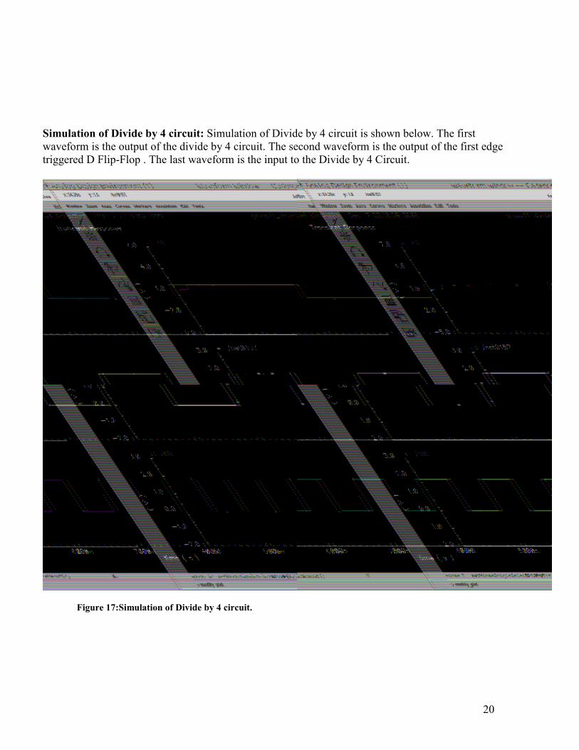
Simulation of Divide by 4 circuit: Simulation of Divide by 4 circuit is shown below. The first
waveform is the output of the divide by 4 circuit. The second waveform is the output of the first edge
triggered D Flip-Flop . The last waveform is the input to the Divide by 4 Circuit.
Figure 17:Simulation of Divide by 4 circuit.
21
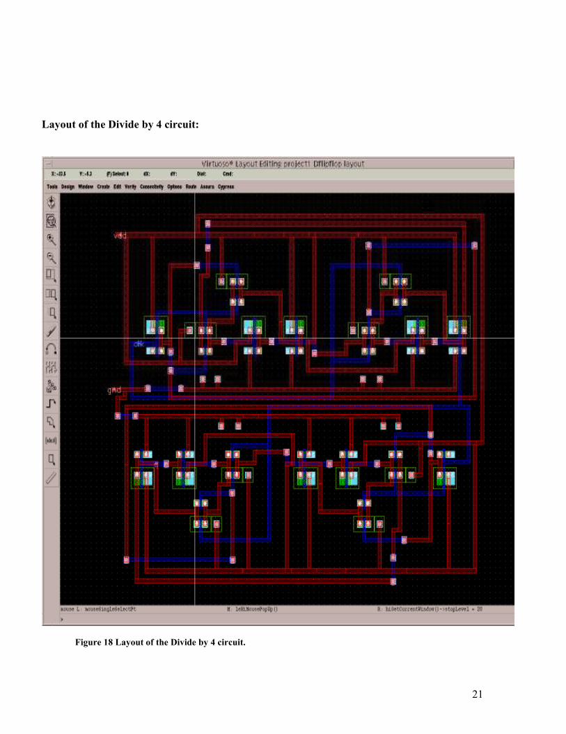
Layout of the Divide by 4 circuit:
Figure 18 Layout of the Divide by 4 circuit.
22
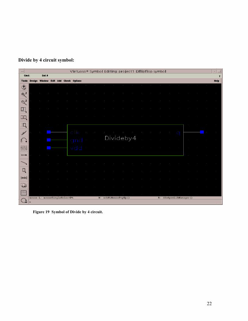
Divide by 4 circuit symbol:
Figure 19 Symbol of Divide by 4 circuit.
23
Corner process
1.62 1.8 1.9 1.98
-40 187.546 58.9029 38.4451 29.3098
0 112.247 45.4726 32.1006 25.5492
27 86.789 39.7151 29.1098 23.7161
70 63.2988 33.4054 25.6395 21.4962
150 42.0275 26.3412 21.4459 18.6198
Table1: typi_typi
-400
2770
150
1.62
1.90
20
40
60
80
100
120
140
160
180
200
time period
temperature(celsius)
voltage
typi_typi
180-200
160-180
140-160
120-140
100-120
80-100
60-80
40-60
20-40
0-20
Figure 20 typi_typi
24
1.62 1.8 1.9 1.98
-40 55.8105 24.8331 18.4274 15.1488
0 40.8973 21.4357 16.6262 14.075
27 34.8257 19.7468 15.6789 13.455
70 28.4418 17.6937 14.4705 12.6412
150 21.5927 15.0609 12.8393 11.4957
Table2: fast_fast
-400
2770
150
1.62
1.90
10
20
30
40
50
60
time period(ns)
temperature(celsius)
voltage
fast_fast
50-60
40-50
30-40
20-30
10-20
0-10
Figure 21 fast_fast
25
1.62 1.8 1.9 1.98
-40 625.942 110.427 54.227 35.3902
0 286.884 74.34 43.016 30.5827
27 192.968 61.0054 38.1172 28.1194
70 119.85 47.6832 32.5038 25.2841
150 64.926 34.412 26.0488 21.5212
Table 3: fast_slow
1.621.8
1.91.98
-40
27
150
0
100
200
300
400
500
600
700
timeperiod(ns)
temperature(celsius)
voltage
fast_slow
600-700
500-600
400-500
300-400
200-300
100-200
0-100
Figure 22 fast_slow

26
1.62 1.8 1.9 1.98
-40 1473.2 260.21 124.081 80.0786
0 607 151.997 85.8969 60.5274
27 386.053 116.921 71.5603 52.5816
70 221.325 85.0668 57.0643 44.1354
150 110.477 56.759 42.4446 34.8982
Table 4: slow_slow
1.621.8
1.91.98
-40
27
150
0
200
400
600
800
1000
1200
1400
1600
time period(ns)
temperature(celsius)
voltage
slow_slow
1400-1600
1200-1400
1000-1200
800-1000
600-800
400-600
200-400
0-200
Figure 23 slow_slow

27
1.62 1.8 1.9 1.98
-40 186.781 74.511 50.4727 38.5504
0 96.0164 49.3071 36.9127 30.077
27 71.6559 40.06957 31.7149 26.5751
70 51.4452 32.4687 26.4121 22.8068
150 34.576 26.574 20.9924 18.708
Table4: slow_fast
1.621.8
1.91.98
-40
27
150
0
20
40
60
80
100
120
140
160
180
200
time period(ns)
temperature(celsius)
voltage
slow_fast
180-200
160-180
140-160
120-140
100-120
80-100
60-80
40-60
20-40
0-20
Figure 24 slow_fast

28