cpe/ee 427, cpe 527, vlsi design i - uah -...
TRANSCRIPT

CPE/EE 427, CPE 527, VLSI Design I: Tutorial #1, Full Custom VLSI (inverter layout)
Joel Wilder, Aleksandar Milenkovic, ECE Dept., The University of Alabama in Huntsville
Adapted from Virginia Tech, Dept. of Electrical Engineering Authors: Meenatchi Jagasivamani and Jos Sulistyo
1. INTRODUCTION In this tutorial, you will learn how to use Cadence Virtuoso to construct a mask level layout of an inverter. You will manually create the artwork, which specifies transistor layouts and their interconnection. You will then add the I/O pins to the inverter and subsequently verify that there are no design rule errors in the final layout.
You will develop a static CMOS inverter onto a p-type silicon substrate; therefore, we will use an NWELL process. Our minimum feature size will be 0.25 microns. It is highly recommended that you read the chapters on CMOS fabrication, layout, and layout design rules in your textbook.
2. CADENCE STARTUP In order to be able to run the Cadence tools, you need to specify a set of environment variables that the tools will need. Do this by editing your .bashrc file in your home directory. At the Unix prompt (indicated by the $ sign) in a terminal window, enter the following:
$ xemacs .bashrc
Add the following two lines at the end of your .bashrc file:
export SKIP_CDS_DIALOG=TRUE
uah-cadence-setup
The SKIP_CDS_DIALOG variable tells Cadence not to display a startup message when opening the tool. The uah-cadence-setup is a script that contains the necessary environment variables for the tool. You will now need to log out of the unix machine, and then log back in in order for the changes to take affect.
After logging back in, in your home directory, create a directory called cadence, where all of your cadence work will be done:
$ mkdir cadence
Change directories into the cadence folder, create a working folder for lab1_2 (you will use the same folder for tutorials 1 and 2), and change directory:
$ cd cadence
$ mkdir lab1_2
$ cd lab1_2
Start the cadence tool by entering the following:
$ icfb&
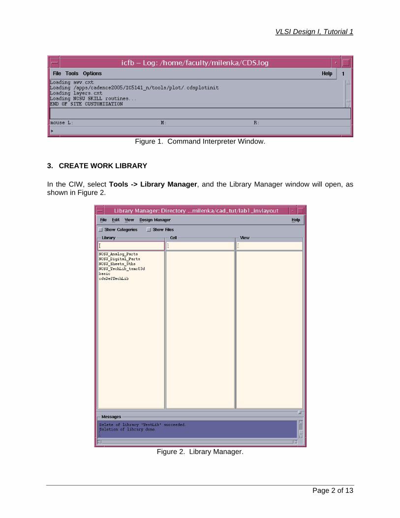
The command interpreter window (CIW) will appear, as shown in Figure 1.
VLSI Design I, Tutorial 1
Figure 1. Command Interpreter Window.
3. CREATE WORK LIBRARY In the CIW, select Tools -> Library Manager, and the Library Manager window will open, as shown in Figure 2.
Figure 2. Library Manager.
Page 2 of 13

VLSI Design I, Tutorial 1
Next, you will create a library, which will be used to contain the inverter that you will construct. This is done through the Library Manager window by selecting File -> New -> Library. A window will open, as shown in Figure 3. Enter TestLib as the name of the library. Leave the path blank, as this will create a folder in your working directory ($HOME/cadence). Attach a Technology Library by selecting the Attach to existing technology library option and using the associated menu to bring up TSMC 0.24u CMOS025/DEEP (5M, HV FET). This will assign the library you are creating to the TSMC 0.25 µm five-metal, 2.5V process. Press OK and you will notice that your Library Window now contains a library called TestLib.
Figure 3. Create Library Window.
4. CREATE INVERTER CELL In the Library Window select TestLib. Then select File -> New -> Cell View and a window will appear as shown in Figure 4. For the Cell Name enter MyINV, and for the Tool, select Virtuoso from the menu.
Page 3 of 13

VLSI Design I, Tutorial 1
Figure 5. Layer Selection Window.
Figure 4. Create Cell Window.
Click OK and two windows will appear. One window is the Layer Selection Window (LSW), which is based on the layers available to the 0.25um process (per the technical library that was attached to the working library, TestLib, that you created), and the other is the Layout Editor window, shown respectively in Figures 5 and 6.
Page 4 of 13

VLSI Design I, Tutorial 1
Figure 6. Layout Editor Window.
5. VIRTUOSO SETUP In the Layout Editor window, select Options -> Display, and set the following options in the window:
1. Pin names: On 2. Minor Spacing : 1.08 3. Major Spacing : 4.32 4. X Snap Spacing: 0.06 5. Y Snap Spacing: 0.06 6. Display levels: 7. From: 0 8. To: 30
Select Save To when you are done. Click OK.
Page 5 of 13

VLSI Design I, Tutorial 1
MOSIS Design Rules
You should follow MOSIS SCN5M_DEEP design rule (http://www.mosis.org/Technical/Layermaps/lm-scmos_scn5m.html) for TSMC 0.25 µm five-metal, 2.5V processing (lambda = 0.12 µm & min. length = 0.24 µm).
The inverter consists of three parts -- PMOS, NMOS, and connections.
This inverter is routed at the minimum size; therefore, the N- and P-MOSFETS have the same W/L.
6. INVERTER LAYOUT As you go through the layout of the inverter, use Figure 7 as a guideline. Remember to save your design often!
Figure 7. Inverter.
Layout Editor Useful Information
• Shortcut keys can be found in the pulldown windows next to the given command
Page 6 of 13

VLSI Design I, Tutorial 1
• ‘f’ fits the design to the editor window size (zoom in/out using the icons on the side toolbar)
• Use the ruler icon for dimensioning. Go to Window->Clear all rulers to delete the ruler markings.
• ‘m’ is used to move an object
Layout of PMOS with L=0.24 µm and W=0.48 µm.
In this tutorial, you are using the NWELL process. Thus, the substrate will be p-substrate. You will create a PMOS transistor first. To do that you will need an NWELL in which the PMOS transistor will be formed. (All work will be done in the Layout Editor window, unless specified for the LSW window.)
Draw the well
a) Select the n-well layer from the LSW window b) Select the Create->Rectangle (or choose the Rectangle icon from the side toolbar or press the shortcut key ‘r’ on your keyboard). c) Using your mouse, draw the n-well on the cellview to be 2.94 wide by 2.52 tall. NOTE: Use dX and dY at the top of the layout editor window to determine the dimensions.
Draw the p-select regions for the PMOS (these regions will contain the diffusion regions)
a) Select the pselect layer from the LSW window; we will draw the pselect enclosing the transistor b) Select the Create->Rectangle (or choose the Rectangle icon from the side toolbar or press the shortcut key ‘r’ on your keyboard). c) Using your mouse, draw the pselect on the cellview: 1.98 wide and 0.96 tall; its left- and right-edges should be 0.48 away from well edges. The pselect should be placed within the n-well, even if the size should vary. (you can use the Edit->move command to move the layer)
Draw Diffusions
a) Select the pactive layer from the LSW window; you will draw the active region of the p-device b) Select the Create->Rectangle (or choose the Rectangle icon from the side toolbar or press the shortcut key ‘r’ on your keyboard). c) Using your mouse, draw the pactive on the cellview to be 1.5 wide by 0.48 tall - it should be enclosed by the pselect by 0.24 and by the nwell by at least 0.72
Draw Poly
a) Select the poly layer from the LSW window b) Select the Create->Rectangle (or choose the Rectangle icon from the side toolbar or press the shortcut key ‘r’ on your keyboard). c) Using your mouse, draw the poly on the cellview to be 0.24 wide by 1.32 long. The poly should be placed at the center of the p-island. The poly should extend over the p-island by 0.30 um.
Page 7 of 13

VLSI Design I, Tutorial 1
Design Rule Check (DRC) As you proceed through your layout, you should periodically perform a DRC in order to correct errors before they build to other errors. Go ahead and perform a DRC on the PMOS that you have just created. Do it again after you create the NMOS.
There are process-specific design rules that describe how close layers can be placed together and what the sizes of the areas can be. These rules give the minimum requirement to avoid a catastrophic failure of your circuit due to fabrication faults. You can use MOSIS SCMOS design rules as a guideline. The design rules are different for different processes.
The following is a procedure to perform design rule check (DRC) for a layout. DRC outputs any violations of the design rules for your technology process. This step is important because the violation of any design rules would cause the fabricated chip to not function as desired.
From your Layout window:
1. Choose Verify -> DRC from the menu. The Verify DRC form will appear. 2. Set the Switch Names field. This switch name depends on the process
you're running. For the HP 0.5 um process:
1. Click on the "Switches" button. 2. Choose the HP14TB switch. 3. Click OK.
For the TSMC 0.35 um and other processes: Leave as default. 3. Click OK to run DRC.
If your design has violated any design rules, DRC will report the errors in the CIW.
Errors are indicated by the markers (white color) on the circuit. You may then proceed to correcting the errors according to the
design rules. 4. For huge layouts,the marker might not be easily located. To find markers,
choose Verify -> Markers -> Find in layout window. A pop up menu will appear. Click on the Zoom to Markers box. Click on the Apply button and Cadence will zoom in to the errors
or warnings as desired.
Layout of NMOS with L=0.24 µm and W=0.48 µm.
Draw the nselect
a) Select the nselect layer from the LSW window b) Select the Create->Rectangle. c) Using your mouse, draw the nselect on the cellview to be 1.98 wide by 0.96 tall
Draw the N active region
a) Select the nactive layer from the LSW window b) Select the Create->Rectangle. c) Using your mouse, draw the nactive on the cellview to be 1.50 wide by 0.48 tall; it should
Page 8 of 13

VLSI Design I, Tutorial 1
be enclosed by the nselect by 0.24 around its edges. Also, it needs to be at least 0.72 away from the n-well (= 6 x lambda; MOSIS rule 2.3 for DEEP).
Extend Poly
Extend the poly layer created for the PMOS over the n-island, making sure that the poly extension over n-island is 0.30. (you can use the Edit->Stretch command to stretch the poly) The poly should be placed at the center of the n-island.
Layout necessary connections Draw the well-contact
a) Select the nselect layer from the LSW window; you will draw the nselect enclosing the substrate (vdd) contact for the PMOS. b) Select the Create->Rectangle. c) Using the mouse, draw the nselect on the cellview; at least 0.96 tall and wide, as it will have to enclose the contact n-active by at least 0.24, which in turn encloses the contact by at least 0.12. The nselect abuts directly to the pselect of the PMOS, but they should not overlap. Also, both selects should be placed within the n-well. d) Select the nactive layer from the LSW window; you will draw the body contact region of the p device. e) Select the Create->Rectangle. f) Using your mouse, draw the nactive on the cellview to be at least 0.48 wide by 0.48 tall
Draw the Substrate-contact
a) Select the pselect layer from the LSW window; you will draw the pselect enclosing the substrate (vss=ground) contact for the NMOS b) Select the Create->Rectangle. c) Using the mouse, draw the pselect on the cellview; at least 0.96 tall and wide, as it will have to enclose the contact p-active by at least 0.24, which in turn encloses the contact by at least 0.12. The pselect abuts directly to the nselect of the NMOS, but they should not overlap. d) Select the pactive layer from the LSW window e) Select the Create->Rectangle. f) Using your mouse, draw the p-island on the cellview to be 0.48 wide by 0.48 tall; it must be enclosed by the pselect by 0.24. The p-island should be placed at least 0.48 um (= 4 x lambda, MOSIS rule 2.5 DEEP) below the NMOS.
Metal Routing
a) Route the metal1 layer from the source of the PMOS to the well-contact. (Make the metal 1 layers 0.48um wide to match the size of the diffusion regions) b) Route the metal1 layer from the source of the NMOS to the substrate-contact. c) Route the metal1 layer from the drain of the PMOS to the drain of the NMOS.
Page 9 of 13

VLSI Design I, Tutorial 1
Place Contacts
Now that all of the layers are in place, contacts should be added to connect the metal1 layer to the p-diffusion and n-diffusion regions. Go to Create->Contact, set the width to 0.24 and the length to 0.24. Choose the correct contact type for each subsequent contact you place: M1_P (metal1 to pactive) and M1_N (metal1 to nactive). Make the contacts for the metal to drains, metal to sources, metal to substrate tap, and metal to well tap.
In preparation for the next section, create a connection point for the input:
a) Create a 0.48x0.48 poly square to serve as an extension to the gate. b) Place an identically sized metal1 square over the poly square you just placed. c) Create an M1_Poly contact here for the input, to connect the metal1 layer to the poly
layer.
Add Pins Once you have finished creating the layout, you need to add pins for the input (named ip), output (named op), vdd! (power), and gnd! (ground). The ‘!’ following the power signals are used to denote global signals. Classify the power signals as inputs. The following is a procedure to add I/O pins to your circuit:
From your Layout window:
1. Choose Create->Pin... from the menu. The Create Pin form will appear. 2. If the form is titled "Create Shape Pin", choose "sym pin" under the Mode
option. 3. Enter a TerminalName(the name of your pin). 4. Make sure that the "Display Pin Name" option is selected. 5. Specify the "I/O Type" as either input, output, or inputoutput. 6. Specify the Pin Type as Metal1, which matches the top layer at the place
that the pin is to be inserted. 7. Specify the Pin Width to 0.24 (the pin is square). 8. Move the mouse to specify where the pin and the label should be placed. 9. Repeat the above process (1-7) for all the pins in your circuit.
Your final inverter layout should look similar to Figure 8.
Page 10 of 13

VLSI Design I, Tutorial 1
Figure 8. Inverter Layout.
7. ASSIGNMENT
• Perform a DRC for the lab instructor to ensure there are no errors with your design. Five points will be deducted for each error in your final design.
• Hand in a printout of your final inverter design.
Page 11 of 13

VLSI Design I, Tutorial 1
NOTE: In order to print out your layout (and schematics, in the future), do the following:
• In the schematic/layout editor in icfb, go to Design->Plot->Submit... (window opens as shown in Figure 9.)
• Select Plot Options..., and fill out the window that opens according to Figure 10.
• OK, then OK. • Go to your terminal window in your working directory and type:
$ lpr accu.ps
Figure 9. Submit Plot Window.
Page 12 of 13

VLSI Design I, Tutorial 1
Figure 10. Plot Options Window.
Page 13 of 13