ee354l final spring2019 -
TRANSCRIPT
May 1, 2019 11:44 am EE354L Final - Spring 2019 1/13 C Copyright 2019 Gandhi Puvvada
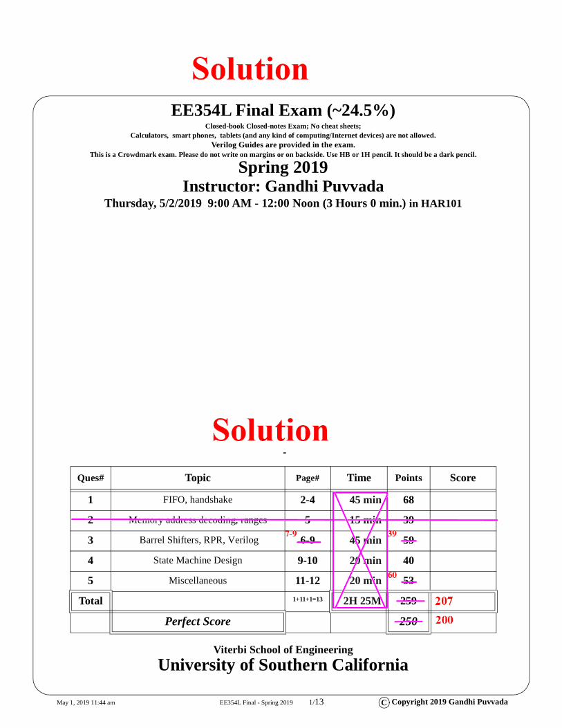
EE354L Final Exam (~24.5%)Closed-book Closed-notes Exam; No cheat sheets;
Calculators, smart phones, tablets (and any kind of computing/Internet devices) are not allowed. Verilog Guides are provided in the exam.
This is a Crowdmark exam. Please do not write on margins or on backside. Use HB or 1H pencil. It should be a dark pencil.
Spring 2019Instructor: Gandhi Puvvada
Thursday, 5/2/2019 9:00 AM - 12:00 Noon (3 Hours 0 min.) in HAR101
Viterbi School of Engineering University of Southern California
Ques# Topic Page# Time Points Score
1 FIFO, handshake 2-4 45 min 68
2 Memory address decoding, ranges 5 15 min 39
3 Barrel Shifters, RPR, Verilog 6-9 45 min 59
4 State Machine Design 9-10 20 min 40
5 Miscellaneous 11-12 20 min 53
Total 1+11+1=13 2H 25M 259
Perfect Score 250
May 1, 2019 11:44 am EE354L Final - Spring 2019 2/13 C Copyright 2019 Gandhi Puvvada
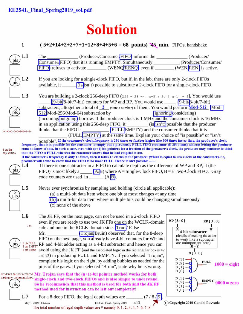
1 ( 5+2+14+2+2+7+1+12+8+4+5+6 = 68 points) 45 min. FIFOs, handshake
1.1 The _____________ (Producer/Consumer/FIFO) informs the _____________ (Producer/Consumer/FIFO) that it is running EMPTY. Simultaneously ___________ (Producer/Consumer/FIFO) refuses to activate ________ (WENQ/RENQ) even if ________ (WEN/REN) is active.
1.2 If you are looking for a single-clock FIFO, but if, in the lab, there are only 2-clock FIFOs available, it ______ (is/isn’t) possible to substitute a 2-clock FIFO for a single-clock FIFO.
1.3 You are building a 2-clock 256-deep FIFO (256 = 28 => (n=8); So [(n+1) = 9]. You would use _____ (9-bit/8-bit/7-bit) counters for WP and RP. You would use _____ (9-bit/8-bit/7-bit) subtracters, altogether a total of ____ (state a number) of them. You would perform ________ (Mod-512/Mod-256/Mod-64) subtraction by _________________ (ignoring/considering) __________ (incoming/outgoing) borrow. If the producer clock is 1 MHz and the consumer clock is 16 MHz in an application using this 256-deep FIFO, it _________ (is/isn’t) possible that the producer thinks that the FIFO is ___________ (FULL/EMPTY) and the consumer thinks that it is ____________ (FULL/EMPTY) at the same time. Explain your choice of "is possible" or "isn’t possible". ____________________________________________________________________ ____________________________________________________________________________ ____________________________________________________________________________
1.4 If there is one subtracter in a FIFO to calculate depth as the difference of WP and RP, it (the FIFO) is most likely a _____ (A/B) where A = Single-Clock FIFO, B = a Two-Clock FIFO. Gray code counters are used in ______ (A/B).
1.5 Never ever synchronize by sampling and holding (circle all applicable):(a) a multi-bit data item where one bit at most changes at any time(b) a multi-bit data item where multiple bits could be changing simultaneously(c) none of the above
1.6 The JK FF, on the next page, can not be used in a 2-clock FIFO even if you are ready to use two JK FFs one on the WCLK-domain side and one in the RCLK domain side. True / FalseMr. _____________ (Trojan/Bruin) observed that, for the 8-deep FIFO on the next page, you already have 4-bit counters for WP and RP and 4-bit adder acting as a 4-bit subtracter and hence you can avoid using the JK FF (and the associated logic in the rectangular boxes #2 and #3) in producing FULL and EMPTY. If you selected "Trojan", complete his logic on the right, by adding bubbles as needed for the pins of the gates. If you selected "Bruin", state why he is wrong. ____________________________________________________ ____________________________________________________ ____________________________________________________
1.7 For a 8-deep FIFO, the legal depth values are _______ (7 / 8 / 9).
5pts
2pts
14pts
2pts
2pts
4-bit subtracter(details of making the adderto work like a subtracterare unimportant here)
X Y
X-Y
WP[3:0] RP[3:0]
D[3:0]
D[3]D[2]D[1]D[0]
FULL
D[3]D[2]D[1]D[0]
EMPTY
7pts
1pts
May 1, 2019 11:44 am EE354L Final - Spring 2019 3/13 C Copyright 2019 Gandhi Puvvada
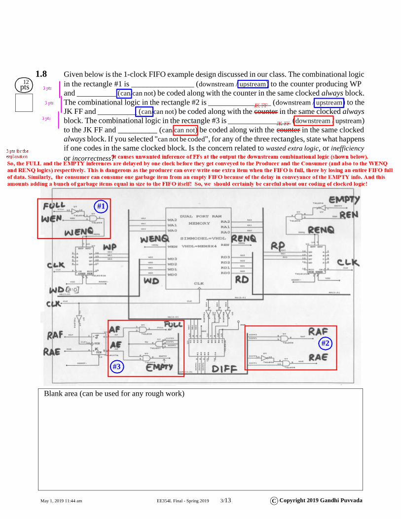
1.8 Given below is the 1-clock FIFO example design discussed in our class. The combinational logic in the rectangle #1 is ________________ (downstream / upstream) to the counter producing WP and __________ (can/can not) be coded along with the counter in the same clocked always block. The combinational logic in the rectangle #2 is ________________ (downstream / upstream) to the JK FF and __________ (can/can not) be coded along with the counter in the same clocked always block. The combinational logic in the rectangle #3 is ________________ (downstream / upstream) to the JK FF and __________ (can/can not) be coded along with the counter in the same clocked always block. If you selected "can not be coded", for any of the three rectangles, state what happens if one codes in the same clocked block. Is the concern related to wasted extra logic, or inefficiency or incorrectness? ______________________________________________________________ ___________________________________________________________________________ ____________________________________________________________________________
12pts
#1
#2
#3
Blank area (can be used for any rough work)
May 1, 2019 11:44 am EE354L Final - Spring 2019 4/13 C Copyright 2019 Gandhi Puvvada
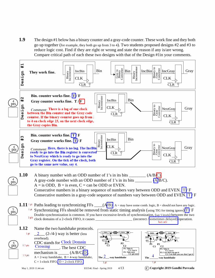
1.9 The design #1 below has a binary counter and a gray-code counter. These work fine and they both go up together (for example, they both go up from 3 to 4). Two students proposed designs #2 and #3 to reduce logic cost. Find if they are right or wrong and state the reason if any is/are wrong. Compare critical path of each these two designs with that of the Design #1in your comments.
1.10 A binary number with an ODD number of 1’s in its bits ________ (A/B/C).A gray-code number with an ODD number of 1’s in its bits ________ (A/B/C).A = is ODD, B = is even, C = can be ODD or EVEN.Consecutive numbers in a binary sequence of numbers vary between ODD and EVEN. T / FConsecutive numbers in a gray-code sequence of numbers vary between ODD and EVEN. T / F
1.11 Paths leading to synchronizing FFs ____(A/B). A = may have some comb. logic, B = should not have any logic. Synchronizing FFs should be removed from static timing analysis (using TIG for timing ignore) T / FDouble-synchronization is common. If you have excessive-levels of synchronization, (say 5 levels) between the two clock domains of a 2-clock FIFO, it causes _____________________ (incorrect / sometimes delayed) operation.
1.12 Name the two handshake protocols. _____ (2-/4-) way is better (less overhead). CDC stands for ____________________________. The best CDC mechanism is _____ (A/B/C/D).A = 2-way handshake, B = 4-way handshake, C = 1-clock FIFO, D = 2-clock FIFO.
4pts
4pts
Gray
CLKGra
y to
Bin
ary
Con
verte
r
Bin
Bin
ary
toG
ray
Con
verte
r
IncGray
Bin
ary
Incr
emen
ter
IncBin
CLR
Bin
CLKBin
ary
Incr
emen
ter
IncBin
CLR
Gray
CLKBin
ary
toG
ray
Con
verte
r
NextGray
Bin
CLKBin
ary
Incr
emen
ter
IncBin
CLR
CLR
Gray
CLKBin
ary
toG
ray
Con
verte
r
NextGray
Bin
CLKBin
ary
Incr
emen
ter
IncBin
CLR
CLR
Design #1
Design #2
Design #3
They work fine.
Bin. counter works fine. T / FGray counter works fine. T / F
Comment: ___________________________________________________________________________________________________________
Bin. counter works fine. T / FGray counter works fine. T / F
Comment: ___________________________________________________________________________________________________________
4pts
5pts
takegot
data_1 data_2
P1 P2C1 C2
The _____-way handshake
P1: Take itC1: Got it
P2: Take nextC2: got next
take
got
data data
P1 P2C1 C2
The _______-way handshake
P1: Take itC1: Got it
P2: I see that you got itC2: I see that you saw that I got it
6pts
May 1, 2019 11:44 am EE354L Final - Spring 2019 5/13 C Copyright 2019 Gandhi Puvvada
2 ( 21 +18 = 39 points) 15 min. Memory address decoding, address ranges
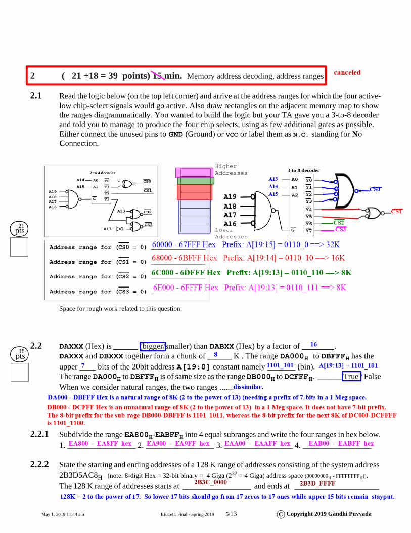
2.1 Read the logic below (on the top left corner) and arrive at the address ranges for which the four active-low chip-select signals would go active. Also draw rectangles on the adjacent memory map to show the ranges diagrammatically. You wanted to build the logic but your TA gave you a 3-to-8 decoder and told you to manage to produce the four chip selects, using as few additional gates as possible. Either connect the unused pins to GND (Ground) or VCC or label them as N.C. standing for No Connection.
Space for rough work related to this question: _____________________________________________________________________________________________________________________________________________________________________________________________________
2.2 DAXXX (Hex) is ______ (bigger/smaller) than DABXX (Hex) by a factor of ________. DAXXX and DBXXX together form a chunk of ______ K . The range DA000H to DBFFFH has the upper ____ bits of the 20bit address A[19:0] constant namely _______ (bin). The range DA000H to DBFFFH is of same size as the range DB000H to DCFFFH. ______ True / FalseWhen we consider natural ranges, the two ranges .......________________________________________________________________________________________________________________________________________________________________________________________________________________________________________________________________________________
2.2.1 Subdivide the range EA800H-EABFFH into 4 equal subranges and write the four ranges in hex below.1. _________________ 2. _________________ 3. _________________ 4. _________________
2.2.2 State the starting and ending addresses of a 128 K range of addresses consisting of the system address 2B3D5AC8H (note: 8-digit Hex = 32-bit binary = 4 Giga (232 = 4 Giga) address space (00000000H - FFFFFFFFH)). The 128 K range of addresses starts at _________________ and ends at _____________________
21pts
Y0A0
G
Y1Y2Y3
A1
3 to 8 decoder
Y4Y5Y6Y7
A2
Address range for (CS0 = 0) _______________
Address range for (CS1 = 0) _______________
Address range for (CS2 = 0) _______________
Address range for (CS3 = 0) _______________
LowerAddresses
HigherAddresses
Y0A0
G
Y1
Y2
Y3
A1
2 to 4 decoder
A19A18A17A16
A13
A13
A14
A15
CS3
CS2
CS1
CS0
18pts
May 1, 2019 11:44 am EE354L Final - Spring 2019 6/13 C Copyright 2019 Gandhi Puvvada
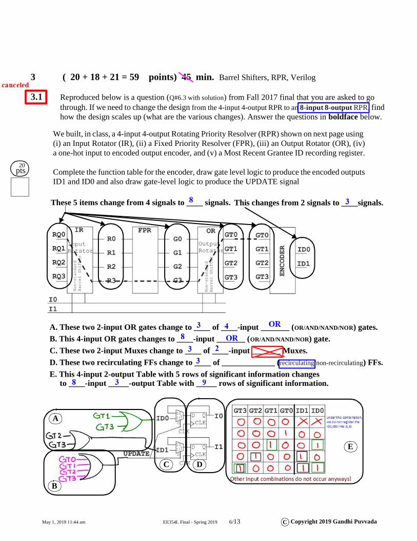
3 ( 20 + 18 + 21 = 59 points) 45 min. Barrel Shifters, RPR, Verilog
3.1 Reproduced below is a question (Q#6.3 with solution) from Fall 2017 final that you are asked to go through. If we need to change the design from the 4-input 4-output RPR to an 8-input 8-output RPR, find how the design scales up (what are the various changes). Answer the questions in boldface below.
20pts
We built, in class, a 4-input 4-output Rotating Priority Resolver (RPR) shown on next page using (i) an Input Rotator (IR), (ii) a Fixed Priority Resolver (FPR), (iii) an Output Rotator (OR), (iv)a one-hot input to encoded output encoder, and (v) a Most Recent Grantee ID recording register.
Complete the function table for the encoder, draw gate level logic to produce the encoded outputsID1 and ID0 and also draw gate-level logic to produce the UPDATE signal
These 5 items change from 4 signals to ____ signals. This changes from 2 signals to ____signals.
A. These two 2-input OR gates change to ____ of ____-input _______ (OR/AND/NAND/NOR) gates.
A
B
B. This 4-input OR gates changes to ____-input _______ (OR/AND/NAND/NOR) gate.
C D
E
C. These two 2-input Muxes change to ____ of ____-input _______ Muxes. D. These two recirculating FFs change to ____ of _____________ (recirculating/non-recirculating) FFs. E. This 4-input 2-output Table with 5 rows of significant information changes to ____-input _____-output Table with _____ rows of significant information.
May 1, 2019 11:44 am EE354L Final - Spring 2019 7/13 C Copyright 2019 Gandhi Puvvada
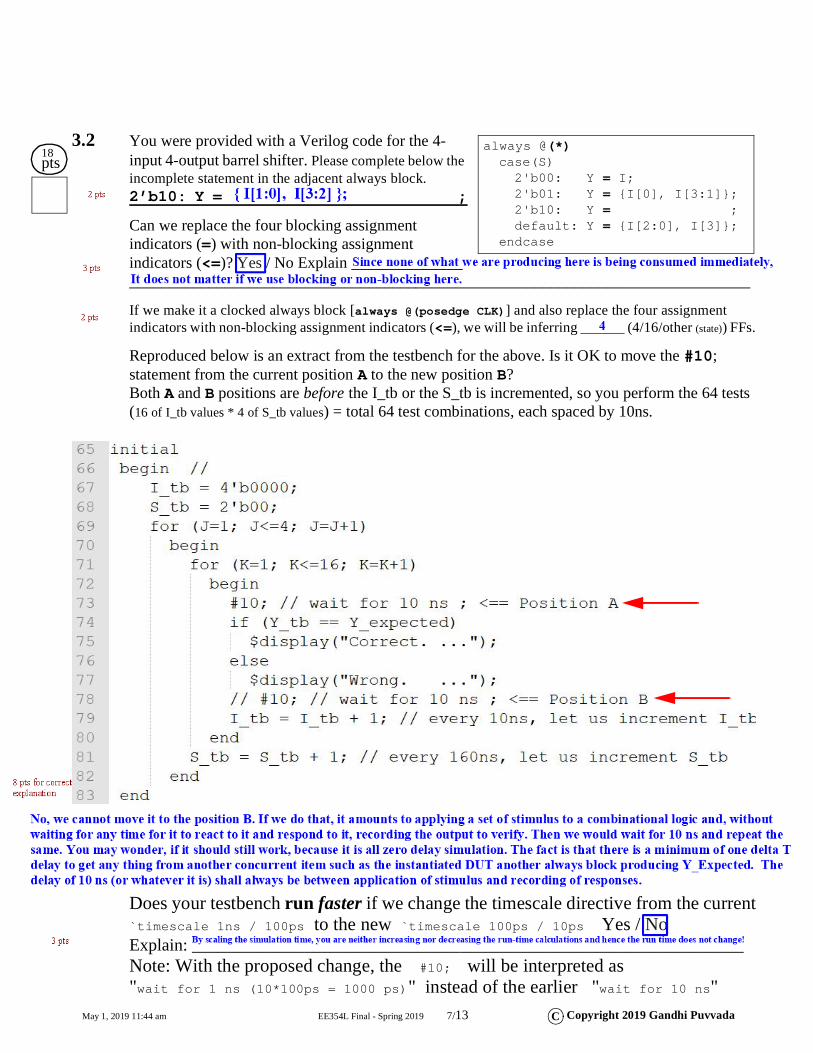
3.2 You were provided with a Verilog code for the 4-input 4-output barrel shifter. Please complete below the incomplete statement in the adjacent always block.2’b10: Y = ;
Can we replace the four blocking assignment indicators (=) with non-blocking assignment indicators (<=)? Yes / No Explain ____________________________________________________________________________________________
If we make it a clocked always block [always @(posedge CLK)] and also replace the four assignment indicators with non-blocking assignment indicators (<=), we will be inferring ______ (4/16/other (state)) FFs.
Reproduced below is an extract from the testbench for the above. Is it OK to move the #10; statement from the current position A to the new position B?Both A and B positions are before the I_tb or the S_tb is incremented, so you perform the 64 tests (16 of I_tb values * 4 of S_tb values) = total 64 test combinations, each spaced by 10ns.
_____________________________________________________________________________ _____________________________________________________________________________ _____________________________________________________________________________ _____________________________________________________________________________ Does your testbench run faster if we change the timescale directive from the current`timescale 1ns / 100ps to the new `timescale 100ps / 10ps Yes / NoExplain: ________________________________________________________________Note: With the proposed change, the #10; will be interpreted as "wait for 1 ns (10*100ps = 1000 ps)" instead of the earlier "wait for 10 ns"
always @(*) case(S) 2'b00: Y = I; 2'b01: Y = {I[0], I[3:1]}; 2'b10: Y = ; default: Y = {I[2:0], I[3]}; endcase
18pts
May 1, 2019 11:44 am EE354L Final - Spring 2019 8/13 C Copyright 2019 Gandhi Puvvada
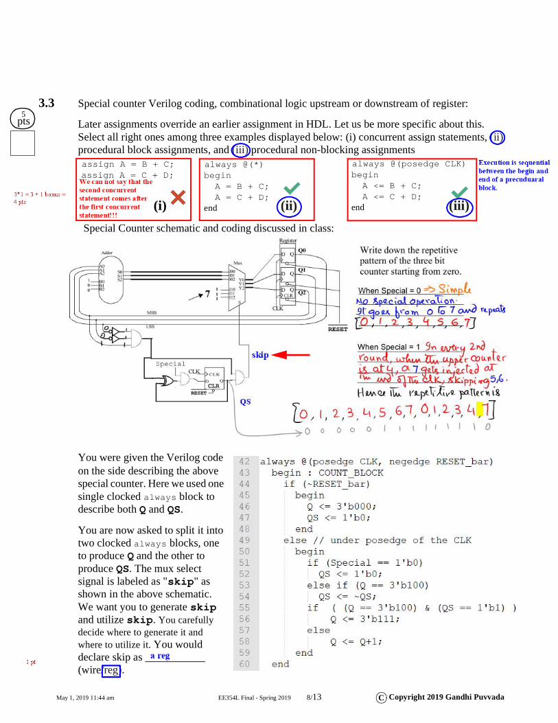
3.3 Special counter Verilog coding, combinational logic upstream or downstream of register:
Later assignments override an earlier assignment in HDL. Let us be more specific about this.Select all right ones among three examples displayed below: (i) concurrent assign statements, (ii) procedural block assignments, and (iii) procedural non-blocking assignments
Special Counter schematic and coding discussed in class:
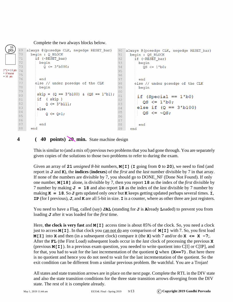
You were given the Verilog code on the side describing the above special counter. Here we used one single clocked always block to describe both Q and QS.
You are now asked to split it into two clocked always blocks, one to produce Q and the other to produce QS. The mux select signal is labeled as "skip" as shown in the above schematic. We want you to generate skip and utilize skip. You carefully decide where to generate it and where to utilize it. You would declare skip as ___________ (wire/reg).
5pts
assign A = B + C;assign A = C + D;
always @(*)begin A = B + C; A = C + D;end
always @(posedge CLK)begin A <= B + C; A <= C + D;end (iii)(i) (ii)
May 1, 2019 11:44 am EE354L Final - Spring 2019 9/13 C Copyright 2019 Gandhi Puvvada
Complete the two always blocks below.
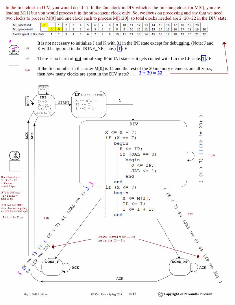
4 ( 40 points) 20 min. State machine design
This is similar to (and a mix of) previous two problems that you had gone through. You are separately given copies of the solutions to those two problems to refer to during the exam.
Given an array of 21 unsigned 8-bit numbers, M[I] (I going from 0 to 20), we need to find (and report in J and K), the indices (indexes) of the first and the last number divisible by 7 in that array. If none of the numbers are divisible by 7, you should go to DONE_NF (Done Not Found). If only one number, M[18] alone, is divisible by 7, then you report 18 as the index of the first divisible by 7 number by making J = 18 and also report 18 as the index of the last divisible by 7 number by making K = 18. So J gets updated only once but K keeps getting updated perhaps several times. I, IP (for I previous), J, and K are all 5-bit in size. I is a counter, where as other three are just registers.
You need to have a Flag, called (say) JAL (standing for J is Already Loaded) to prevent you from loading J after it was loaded for the first time.
Here, the clock is very fast and M[I] access time is about 85% of the clock. So, you need a clock just to access M[I]. In that clock you can not do any comparison of M[I] with 7. So, you first load M[I] into X and then (in a subsequent clock) compare it (the X) with 7 and/or do X <= X -7;.After the FL (the First Load) subsequent loads occur in the last clock of processing the previous X (previous M[I]). In a previous exam question, you needed to write quotient into C[I] or C[IP], and for that, you had to wait for the last incrementation of the quotient Q when (X==7). But here there is no quotient and hence you do not need to wait for the last incrementation of the quotient. So the exit condition can be different from a similar previous problem. Be watchful. You are a Trojan!
All states and state transition arrows are in place on the next page. Complete the RTL in the DIV state and also the state transition conditions for the three state transition arrows diverging from the DIV state. The rest of it is complete already.
16pts
May 1, 2019 11:44 am EE354L Final - Spring 2019 10/13 C Copyright 2019 Gandhi Puvvada
It is not necessary to initialize J and K with 31 in the INI state except for debugging. (Note: J and K will be ignored in the DONE_NF state.) T / F
There is no harm of not initializing IP in INI state as it gets copied with I in the LF state. T / F
If the first number in the array M[0] is 14 and the rest of the 20 memory elements are all zeros, then how many clocks are spent in the DIV state? ________________
4pts
I<=0;J<=31;K<=31;
INI
START
START
RES
ET
LF(Load First)
DIV
DONE_F DONE_NF
ACK
ACK
ACK
ACK
ACK
X <= M[I];IP <= I;I <=I + 1;
JAL<=0;
1
35pts
May 1, 2019 11:44 am EE354L Final - Spring 2019 11/13 C Copyright 2019 Gandhi Puvvada
5 ( 10+6+4+12+21 = 53 points) 20 min. Miscellaneous
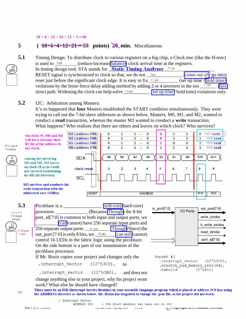
5.1 Timing Design: To distribute clock to various registers on a big chip, a Clock tree (like the H-tree) is used to _________ (reduce/increase/balance) clock arrival time at the registers. In timing design tool, STA stands for ____________________________________________RESET signal is synchronized to clock so that, we do not _______________ (come out of / go into) reset just before the significant clock edge. It is easy to fix ____________ (set up time / hold time) violations by the brute-force delay adding method by adding 2 or 4 inverters in the too _______ (fast/slow) path. Widening the clock can help solve ___________ (set up time / hold time) violations only.
5.2 I2C: Arbitration among Masters:It’s so happened that four Masters established the START condition simultaneously. They were trying to call out the 7-bit slave addresses as shown below. Masters, M0, M1, and M2, wanted to conduct a read transaction, whereas the master M3 wanted to conduct a write transaction. What happens? Who realizes that there are others and leaves on which clock? Who survives?
5.3 Picoblaze is a ________________ (soft-core/hard-core) processor. _____________ (Because/Though) the 8-bit port_id[7:0] is common to both input and output ports, we _________ (can/cannot) have 256 separate input ports and 256 separate output ports. __________ (Though/Since) the out_port [7:0] is only 8 bits, we ________ (can still/cannot) control 16 LEDs in the fabric logic using the picoblaze. On the side bottom is a part of our instantiation of the picoblaze processor. If Mr. Bruin copies your project and changes only the
to
and does not change anything else in your project, why his project wont work? What else he should have changed?_______________________________________________________________________________ _______________________________________________________________________________ _______________________________________________________________________________
10pts
6pts
12pts
May 1, 2019 11:44 am EE354L Final - Spring 2019 12/13 C Copyright 2019 Gandhi Puvvada
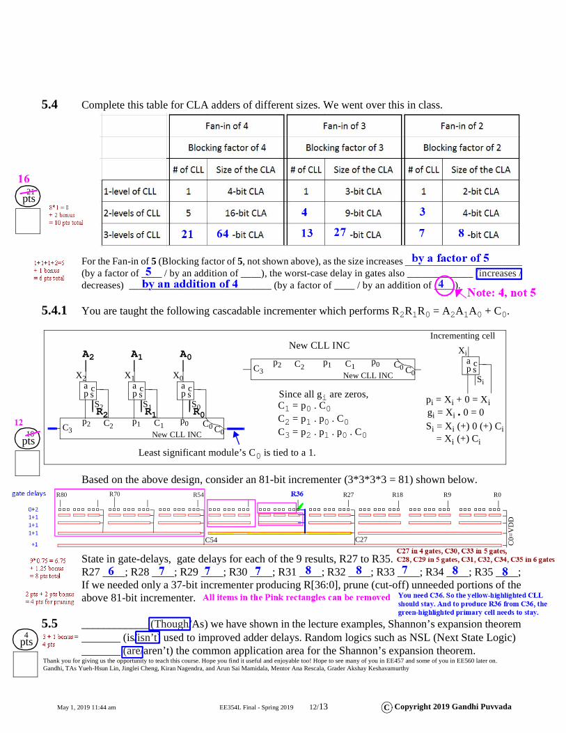
5.4 Complete this table for CLA adders of different sizes. We went over this in class.
For the Fan-in of 5 (Blocking factor of 5, not shown above), as the size increases _______________________ (by a factor of ____ / by an addition of ____), the worst-case delay in gates also _____________ (increases / decreases) ____________________________ (by a factor of ____ / by an addition of ____).
5.4.1 You are taught the following cascadable incrementer which performs R2R1R0 = A2A1A0 + C0.
Based on the above design, consider an 81-bit incrementer (3*3*3*3 = 81) shown below.
State in gate-delays, gate delays for each of the 9 results, R27 to R35.R27 ____; R28 ____; R29 ____; R30 ____; R31 ____; R32 ____; R33 ____; R34 ____; R35 ____; If we needed only a 37-bit incrementer producing R[36:0], prune (cut-off) unneeded portions of the above 81-bit incrementer.
5.5 ____________ (Though/As) we have shown in the lecture examples, Shannon’s expansion theorem _______ (is/isn’t) used to improved adder delays. Random logics such as NSL (Next State Logic) _______ (are/aren’t) the common application area for the Shannon’s expansion theorem.
21pts
10pts
ap sc
X2
S2
ap sc
X1
S1
ap sc
X0
S0
p0p1p2 C2 C1 C0 C0C3 New CLL INC
A2 A1 A0
R2 R1 R0
ap s
cXi
Si
Si = Xi (+) 0 (+) Ci
Incrementing cell
= Xi (+) Ci
pi = Xi + 0 = Xigi = Xi . 0 = 0
p0p1p2 C2 C1 C0 C0C3 New CLL INC
New CLL INC
Since all gi are zeros, C1 = p0 . C0C2 = p1 . p0 . C0C3 = p2 . p1 . p0 . C0
Least significant module’s C0 is tied to a 1.
R0R9R18R27R54R80
C0=
VD
D
C27C54
R70
4pts
Thank you for giving us the opportunity to teach this course. Hope you find it useful and enjoyable too! Hope to see many of you in EE457 and some of you in EE560 later on.Gandhi, TAs Yueh-Hsun Lin, Jinglei Cheng, Kiran Nagendra, and Arun Sai Mamidala, Mentor Ana Rescala, Grader Akshay Keshavamurthy

May 1, 2019 11:44 am EE354L Final - Spring 2019 13/13 C Copyright 2019 Gandhi Puvvada
Blank page: Please write your name and email. Tear it off and use it for rough work. Do not submit at the end. Keep it with you.
Student’s Last Name:____________________ email: __________________