el9200, el9201, el9202 datasheet - renesas electronics · 2018-08-03 · ictl ctl input current ctl...
TRANSCRIPT
FN7438Rev 1.00
October 30, 2008
EL9200, EL9201, EL9202 Programmable VCOM
DATASHEET
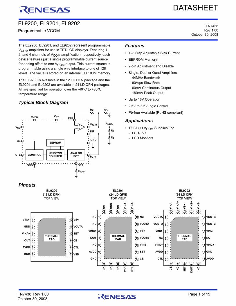
The EL9200, EL9201, and EL9202 represent programmable VCOM amplifiers for use in TFT-LCD displays. Featuring 1, 2, and 4 channels of VCOM amplification, respectively, each device features just a single programmable current source for adding offset to one VCOM output. This current source is programmable using a single wire interface to one of 128 levels. The value is stored on an internal EEPROM memory.
The EL9200 is available in the 12 LD DFN package and the EL9201 and EL9202 are available in 24 LD QFN packages. All are specified for operation over the -40°C to +85°C temperature range.
Typical Block Diagram
Features
• 128 Step Adjustable Sink Current
• EEPROM Memory
• 2-pin Adjustment and Disable
• Single, Dual or Quad Amplifiers
- 44MHz Bandwidth
- 80V/µs Slew Rate
- 60mA Continuous Output
- 180mA Peak Output
• Up to 18V Operation
• 2.6V to 3.6VLogic Control
• Pb-free Available (RoHS compliant)
Applications
• TFT-LCD VCOM Supplies For
- LCD-TVs
- LCD Monitors
-+
EEPROM
CONTROLUP/DOWNCOUNTER
ANALOGPOTCTL
CE
VSD
AVDD
GND SET
RSET
IOUT
INP
VOUT
INN
RF RG
R1
R2
AVDD
VS+
GND
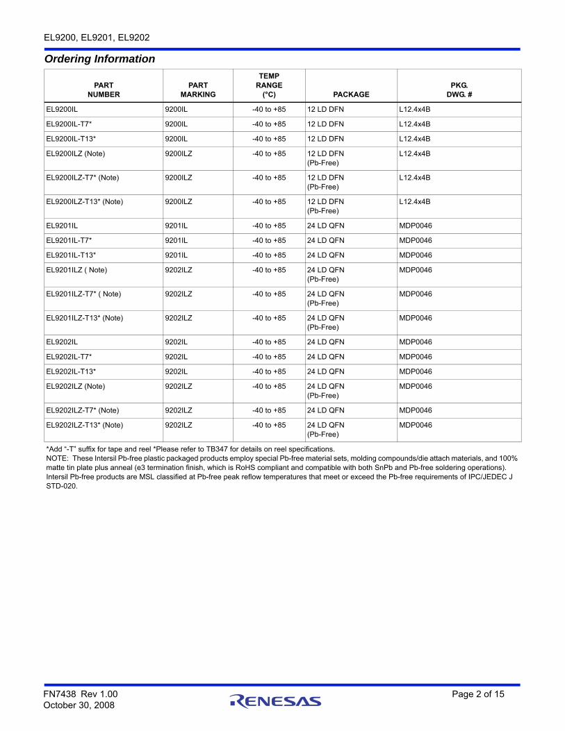
PinoutsEL9200
(12 LD DFN)TOP VIEW
EL9201(24 LD QFN)TOP VIEW
EL9202(24 LD QFN)TOP VIEW
12
11
10
9
8
7
1
2
3
4
5
6
THERMAL PAD
VINA-
GND
VINA+
IOUT
AVDD
GND
VS+
VOUTA
SET
CE
CTL
VSD
19
18
17
16
15
14
13
24
23
22
21
20
8 9 10
11
12
1
2
3
4
5
6
7
NC
NC
VINB+
IOUT
NC
AVDD
GND
NC
VOUTA
VS+
VOUTB
VINB-
SET
CE
NC
GN
D
NC
VIN
A+
VIN
A-
NC
NC
NC
VS
D
CT
L
THERMAL PAD
19
18
17
16
15
14
13
24
23
22
21
20
8 9 10
11
12
1
2
3
4
5
6
7
VOUTA
VOUTD
VIND-
NC
VIND+
AVDD
CTL
VOUTB
VOUTC
VINC-
NC
VINC+
GND
AVDD
VIN
A-
VIN
A+
VS
+
VIN
B+
VIN
B-
CE
NC
SE
T
IOU
T
NC
THERMAL PAD
FN7438 Rev 1.00 Page 1 of 15October 30, 2008
EL9200, EL9201, EL9202
Ordering Information
PART NUMBER
PARTMARKING
TEMP RANGE
(°C) PACKAGEPKG.
DWG. #
EL9200IL 9200IL -40 to +85 12 LD DFN L12.4x4B
EL9200IL-T7* 9200IL -40 to +85 12 LD DFN L12.4x4B
EL9200IL-T13* 9200IL -40 to +85 12 LD DFN L12.4x4B
EL9200ILZ (Note) 9200ILZ -40 to +85 12 LD DFN(Pb-Free)
L12.4x4B
EL9200ILZ-T7* (Note) 9200ILZ -40 to +85 12 LD DFN(Pb-Free)
L12.4x4B
EL9200ILZ-T13* (Note) 9200ILZ -40 to +85 12 LD DFN(Pb-Free)
L12.4x4B
EL9201IL 9201IL -40 to +85 24 LD QFN MDP0046
EL9201IL-T7* 9201IL -40 to +85 24 LD QFN MDP0046
EL9201IL-T13* 9201IL -40 to +85 24 LD QFN MDP0046
EL9201ILZ ( Note) 9202ILZ -40 to +85 24 LD QFN(Pb-Free)
MDP0046
EL9201ILZ-T7* ( Note) 9202ILZ -40 to +85 24 LD QFN(Pb-Free)
MDP0046
EL9201ILZ-T13* (Note) 9202ILZ -40 to +85 24 LD QFN(Pb-Free)
MDP0046
EL9202IL 9202IL -40 to +85 24 LD QFN MDP0046
EL9202IL-T7* 9202IL -40 to +85 24 LD QFN MDP0046
EL9202IL-T13* 9202IL -40 to +85 24 LD QFN MDP0046
EL9202ILZ (Note) 9202ILZ -40 to +85 24 LD QFN(Pb-Free)
MDP0046
EL9202ILZ-T7* (Note) 9202ILZ -40 to +85 24 LD QFN MDP0046
EL9202ILZ-T13* (Note) 9202ILZ -40 to +85 24 LD QFN(Pb-Free)
MDP0046
*Add “-T” suffix for tape and reel *Please refer to TB347 for details on reel specifications.NOTE: These Intersil Pb-free plastic packaged products employ special Pb-free material sets, molding compounds/die attach materials, and 100% matte tin plate plus anneal (e3 termination finish, which is RoHS compliant and compatible with both SnPb and Pb-free soldering operations). Intersil Pb-free products are MSL classified at Pb-free peak reflow temperatures that meet or exceed the Pb-free requirements of IPC/JEDEC J STD-020.
FN7438 Rev 1.00 Page 2 of 15October 30, 2008

EL9200, EL9201, EL9202
Absolute Maximum Ratings (TA = +25°C) Thermal Information
VS+ Supply Voltage between VS+ and GND . . . . . . . . . . . . . .18VSupply Voltage between VSD and GND . . . . . . . . . . . . . . . . . . . .4VMaximum Continuous Output Current . . . . . . . . . . . . . . . . . . . 65mAInput Voltages to GND
SET, CE . . . . . . . . . . . . . . . . . . . . . . . . . . . . . . . . . . . -0.3V to +4VCTL. . . . . . . . . . . . . . . . . . . . . . . . . . . . . . . . . . . . . . -0.3V to +16V
Output Voltages to GNDOUT . . . . . . . . . . . . . . . . . . . . . . . . . . . . . . . . . . . . . -0.3V to +20V
AVDD . . . . . . . . . . . . . . . . . . . . . . . . . . . . . . . . . . . . . . -0.3V to +20VESD Rating
Human Body Model . . . . . . . . . . . . . . . . . . . . . . . . . . . . . . . . .2kV
Maximum Die Temperature . . . . . . . . . . . . . . . . . . . . . . . . . . +150°CStorage Temperature . . . . . . . . . . . . . . . . . . . . . . . . -65°C to +150°CPb-Free Reflow Profile. . . . . . . . . . . . . . . . . . . . . . . . .see link below
http://www.intersil.com/pbfree/Pb-FreeReflow.asp
Operating ConditionsAmbient Operating Temperature . . . . . . . . . . . . . . . . -40°C to +85°C
CAUTION: Do not operate at or near the maximum ratings listed for extended periods of time. Exposure to such conditions may adversely impact product reliability andresult in failures not covered by warranty.
IMPORTANT NOTE: All parameters having Min/Max specifications are guaranteed. Typical values are for information purposes only. Unless otherwise noted, all testsare at the specified temperature and are pulsed tests, therefore: TJ = TC = TA
Electrical Specifications VSD = 3V, VS+ = 15V, AVDD = 15V, RSET = 24.9k, and TA = +25°C unless otherwise specified.
PARAMETER DESCRIPTION CONDITION MIN TYP MAX UNIT
VS+ Supply Voltage 4.5 16.5 V
IS+ Quiescent Current EL9200 3.8 4.8 mA
EL9201 7.6 9.6 mA
EL9202 10.5 16 mA
VSD Logic Supply Voltage For programming 3 3.6 V
For operation 2.6 3.6 V
ISD Quiescent Logic Current CE = 3.6V 50 µA
CE = GND 25 µA
Program (charge pump current) (Note 1) 23 mA
Read (Note 1) 3 mA
IADD Supply Current (Note 2) 25 µA
CTLIH CTL High Voltage 2.6V < VSD < 3.6V 0.7*VSD 0.8*VSD V
CTLIL CTL Low Voltage 2.6V < VSD < 3.6V 0.2*VSD 0.3*VSD V
CTLIHRPW CTL High Rejected Pulse Width 20 µs
CTLILRPW CTL Low Rejected Pulse Width 20 µs
CTLIHMPW CTL High Minimum Pulse Width 200 µs
CTLILMPW CTL Low Minimum Pulse Width 200 µs
CTLMTC CTL Minimum Time Between Counts 10 µs
ICTL CTL Input Current CTL = GND 10 µA
CTL = VSD 10 µA
CTLCAP CTL Input Capacitance 10 pF
CEIL CE Input Low Voltage 2.6V < VSD < 3.6V 0.4 V
CEIH CE Input High Voltage 2.6V < VSD < 3.6V 1.6 V
CEST CE Minimum Start-Up Time (Note 1) 1 ms
CTLPROM CTL EEPROM Program Voltage 2.6V < VSD < 3.6V (Note 2) 4.9 15.75 V
CTLPT CTL EEPROM Programming Signal Time
> 4.9V 200 µs
PT Programming Time 100 ms
EEWC EE Write Cycles (Note 5) 1000 cycles
FN7438 Rev 1.00 Page 3 of 15October 30, 2008
EL9200, EL9201, EL9202
SETDN SET Differential Nonlinearity Monotonic over-temperature ±1 LSB
SETZSE SET Zero-Scale Error (Note 3) ±2 LSB
SETFSE SET Full-Scale Error (Note 3) ±8 LSB
ISET SET Current Through RSET (Note 1) 120 µA
SETER SET External Resistance To GND, AVDD = 20V (Note 1) 10 200 k
To GND, AVDD = 4.5V (Note 1) 2.25 45 k
AVDD to SET AVDD to SET Voltage Attenuation 1:20 V/V
OUTST OUT Settling Time To ±0.5 LSB error band (Note 1) 20 µs
VOUT OUT Voltage Range (Note 1) VSET + 0.5V 13 V
OUTVD OUT Voltage Drift (Note 1) 10 mV
AMPLIFIER CHARACTERISTICS
INPUT CHARACTERISTICS
VOS Input Offset Voltage VCM = 0V 3 15 mV
TCVOS Average Offset Voltage Drift (Note 1) 7 µV/°C
IB Input Bias Current VCM = 0V 2 60 nA
RIN Input Impedance 1 G
CIN Input Capacitance 2 pF
CMRR Common-Mode Rejection Ratio For VIN from -5.5V to +5.5V 50 70 dB
AVOL Open-Loop Gain -4.5V VOUT +4.5V 60 70 dB
OUTPUT CHARACTERISTICS
VOL Output Swing Low RL = 1.5k to 0 0.09 0.15 V
VOH Output Swing High 14.85 14.9 V
ISC Short-Circuit Current ±150 ±180 mA
IOUT Output Current ±65 mA
POWER SUPPLY PERFORMANCE
PSRR Power Supply Rejection Ratio VS+ is moved from 4.5V to 15.5V 55 80 dB
DYNAMIC PERFORMANCE
SR Slew Rate (Note 4) -4.0V VOUT 4.0V, 20% to 80% 60 80 V/µs
tS Settling to +0.1% (AV = +1) (AV = +1), VOUT = 2V step 80 ns
BW -3dB Bandwidth 44 MHz
GBWP Gain-Bandwidth Product 32 MHz
PM Phase Margin 50 °
CS Channel Separation f = 5MHz (EL9201 and EL9202 only) 110 dB
dG Differential Gain (Note 5) RF = RG = 1kand VOUT = 1.4V 0.17 %
dP Differential Phase (Note 5) RF = RG = 1kand VOUT = 1.4V 0.24 °
NOTES:
1. Simulated and determined via design and not directly tested
2. Tested at AVDD = 20V
3. Wafer sort only
4. NTSC signal generator used
5. Limits established by characterization and are not production tested.
Electrical Specifications VSD = 3V, VS+ = 15V, AVDD = 15V, RSET = 24.9k, and TA = +25°C unless otherwise specified. (Continued)
PARAMETER DESCRIPTION CONDITION MIN TYP MAX UNIT
FN7438 Rev 1.00 Page 4 of 15October 30, 2008
EL9200, EL9201, EL9202
Pin Descriptions
PIN IN/OUT DESCRIPTION EQUIVALENT CIRCUIT
VINx- Input Amplifier x inverting input, where:x = A for EL9200x = A, B for EL9201x = A, B, C, D for EL9202
VINx+ Input Amplifier x non-inverting input, where:x = A for EL9200x = A, B for EL9201x = A, B, C, D for EL9202
Reference Circuit 1
VS+ Supply Op amp supply; bypass to GND with 0.1µF capacitor
VOUTX Output Amplifier X output, where:x = A for EL9200x = A, B for EL9201x = A, B, C, D for EL9202
NC - No connect; not internally connected
GND Supply Ground connection
IOUT Output Adjustable sink current output pin; the current sinks into the OUT pin is equal to the DAC setting times the maximum adjustable sink current divided by 128; see SET pin function description for the maxim adjustable sink current setting
SET Output Maximum sink current adjustment point; connect a resistor from SET to GND to set the maximum adjustable sink current of the OUT pin; the maximum adjustable sink current is equal to (AVDD/20) divided by RSET
CE Input Counter enable pin; connect CE to VDD to enable counting of the internal counter; connect CE to GND to inhibit counting
CTL Input Internal counter up/down control and internal EEPROM programming control input; if CE is high, a mid-to-low transition increments the 7-bit counter, raising the DAC setting, increasing the OUT sink current, and lowering the divider voltage at OUT; a mid-to-high transition decrements the 7-bit counter, lowering the DAC setting, decreasing the OUT sink current, and increasing the divider voltage at OUT; applying 4.9V and above with appropriately arranged timing will overwrite EEPROM with the contents in the 7-bit counter; see EEPROM Programming section for details
AVDD Supply Analog voltage supply; bypass to GND with 0.1µF capacitor
VSD Supply System power supply input; bypass to GND with 0.1µF capacitor
VS+
GND
CIRCUIT 1
VS+
GNDGND
CIRCUIT 2
FN7438 Rev 1.00 Page 5 of 15October 30, 2008
EL9200, EL9201, EL9202
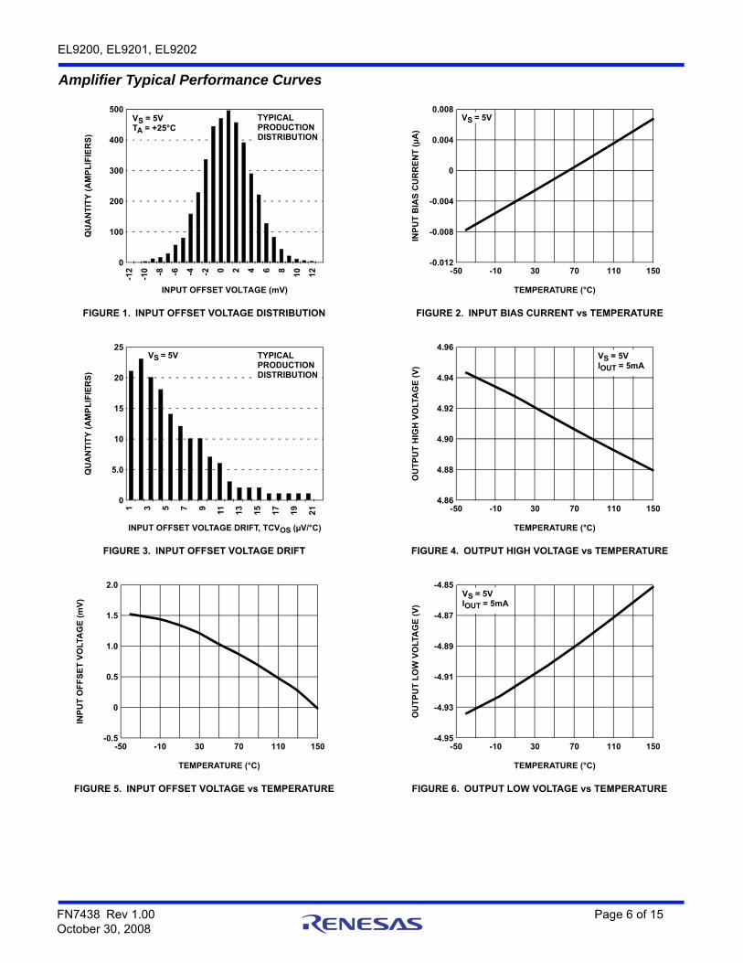
Amplifier Typical Performance Curves
FIGURE 1. INPUT OFFSET VOLTAGE DISTRIBUTION FIGURE 2. INPUT BIAS CURRENT vs TEMPERATURE
FIGURE 3. INPUT OFFSET VOLTAGE DRIFT FIGURE 4. OUTPUT HIGH VOLTAGE vs TEMPERATURE
FIGURE 5. INPUT OFFSET VOLTAGE vs TEMPERATURE FIGURE 6. OUTPUT LOW VOLTAGE vs TEMPERATURE
QU
AN
TIT
Y (
AM
PL
IFIE
RS
)
500
400
300
200
100
0
-12
-10 -8 -6 -4 -2 0 2 4 6 8 10 12
INPUT OFFSET VOLTAGE (mV)
VS = 5VTA = +25°C
TYPICAL PRODUCTION DISTRIBUTION
VS = 5V
INP
UT
BIA
S C
UR
RE
NT
(µ
A)
0.008
0.004
0
-0.004
-0.008
-0.012-50 -10 30 70 110 150
TEMPERATURE (°C)
VS = 5V TYPICAL PRODUCTION DISTRIBUTION
QU
AN
TIT
Y (
AM
PL
IFIE
RS
)
25
20
15
10
5.0
0
1 3 5 7 9 11 13
15
17
19
21
INPUT OFFSET VOLTAGE DRIFT, TCVOS (µV/°C)
VS = 5VIOUT = 5mA
OU
TP
UT
HIG
H V
OLT
AG
E (
V)
4.96
4.94
4.92
4.90
4.88
4.86-50 -10 30 70 110 150
TEMPERATURE (°C)
INP
UT
OF
FS
ET
VO
LTA
GE
(m
V)
2.0
1.5
1.0
0.5
0
-0.5-50 -10 30 70 110 150
TEMPERATURE (°C)
VS = 5VIOUT = 5mA
OU
TP
UT
LO
W V
OLT
AG
E (
V)
-4.85
-4.87
-4.89
-4.91
-4.93
-4.95-50 -10 30 70 110 150
TEMPERATURE (°C)
FN7438 Rev 1.00 Page 6 of 15October 30, 2008
EL9200, EL9201, EL9202
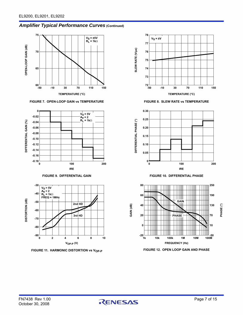
FIGURE 7. OPEN-LOOP GAIN vs TEMPERATURE FIGURE 8. SLEW RATE vs TEMPERATURE
FIGURE 9. DIFFERENTIAL GAIN FIGURE 10. DIFFERENTIAL PHASE
FIGURE 11. HARMONIC DISTORTION vs VOP-P FIGURE 12. OPEN LOOP GAIN AND PHASE
Amplifier Typical Performance Curves (Continued)O
PE
N-L
OO
P G
AIN
(d
B)
75
70
65
60-50 -10 30 70 110 150
TEMPERATURE (°C)
VS = ±5VRL = 1k
VS = ±V
SL
EW
RA
TE
(V
/µs
)
78
77
76
75
74
72-50 -10 30 70 110 150
TEMPERATURE (°C)
73
VS = 5VAV = 2RL = 1k
DIF
FE
RE
NT
IAL
GA
IN (
%)
0
-0.02
-0.04
-0.12
-0.14
-0.180 100 200
IRE
-0.16
-0.06
-0.08
-0.10D
IFF
ER
EN
TIA
L P
HA
SE
(°)
0.30
0.25
0.20
0.05
00 100 200
IRE
0.15
0.10
VS = 5VAV = 2RL = 1kFREQ = 1MHz
2nd HD
3rd HD
DIS
TO
RT
ION
(d
B)
-30
-40
-50
-80
-900 8 10
VOP-P (V)
-60
-70
2 4 6
GAIN
PHASE
1k 10M 100M
FREQUENCY (Hz)
10k 100k 1M
GA
IN (
dB
)
80
60
40
-20
20
0
250
190
130
-50
70
10
PH
AS
E (
°)
FN7438 Rev 1.00 Page 7 of 15October 30, 2008
EL9200, EL9201, EL9202
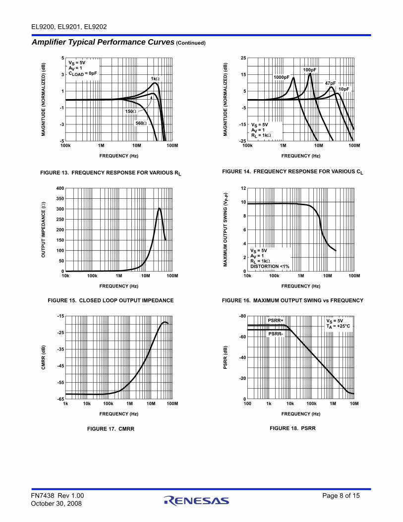
FIGURE 13. FREQUENCY RESPONSE FOR VARIOUS RL FIGURE 14. FREQUENCY RESPONSE FOR VARIOUS CL
FIGURE 15. CLOSED LOOP OUTPUT IMPEDANCE FIGURE 16. MAXIMUM OUTPUT SWING vs FREQUENCY
FIGURE 17. CMRR FIGURE 18. PSRR
Amplifier Typical Performance Curves (Continued)
VS = 5VAV = 1 CLOAD = 0pF
1k
560
150
100k 100M
FREQUENCY (Hz)
1M 10M
MA
GN
ITU
DE
(N
OR
MA
LIZ
ED
) (d
B)
5
3
1
-5
-1
-3 VS = 5VAV = 1 RL = 1k
10pF47pF
100pF
1000pF
100k 100M
FREQUENCY (Hz)
1M 10M
MA
GN
ITU
DE
(N
OR
MA
LIZ
ED
) (d
B)
25
15
5
-25
-5
-15
10k 100M
FREQUENCY (Hz)
100k 10M
OU
TP
UT
IM
PE
DA
NC
E (
)
400
350
250
0
200
150
1M
100
50
300
VS = 5VAV = 1RL = 1kDISTORTION <1%
10k 100M
FREQUENCY (Hz)
100k 10M
MA
XIM
UM
OU
TP
UT
SW
ING
(V
P-P
)
12
10
6
0
4
2
1M
8
1k 100M
FREQUENCY (Hz)
100k 10M
CM
RR
(d
B)
-15
-25
-45
-65
-55
1M
-35
10k
PSRR+ VS = 5VTA = +25°C
PSRR-
100 10M
FREQUENCY (Hz)
10k 1M100k1k
PS
RR
(d
B)
-80
-60
-20
0
-40
FN7438 Rev 1.00 Page 8 of 15October 30, 2008
EL9200, EL9201, EL9202
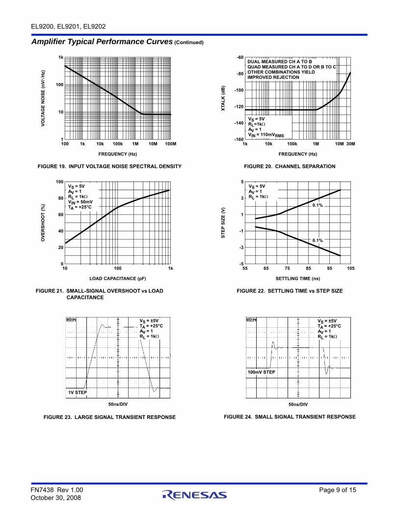
FIGURE 19. INPUT VOLTAGE NOISE SPECTRAL DENSITY FIGURE 20. CHANNEL SEPARATION
FIGURE 21. SMALL-SIGNAL OVERSHOOT vs LOAD CAPACITANCE
FIGURE 22. SETTLING TIME vs STEP SIZE
FIGURE 23. LARGE SIGNAL TRANSIENT RESPONSE FIGURE 24. SMALL SIGNAL TRANSIENT RESPONSE
Amplifier Typical Performance Curves (Continued)
100 100M
FREQUENCY (Hz)
10k 1M100k1k
VO
LTA
GE
NO
ISE
(n
V/
Hz)
1k
100
1
10
10M 1k 30M
FREQUENCY (Hz)
100k 10M1M10k
XTA
LK
(d
B)
-60
-80
-140
-160
-120
-100
DUAL MEASURED CH A TO BQUAD MEASURED CH A TO D OR B TO COTHER COMBINATIONS YIELD IMPROVED REJECTION
VS = 5VRL=1kAV = 1VIN = 110mVRMS
VS = 5VAV = 1RL = 1kVIN = 50mVTA = +25°C
10 1k
LOAD CAPACITANCE (pF)
100
OV
ER
SH
OO
T (
%)
100
60
0
20
80
40
VS = 5VAV = 1RL = 1k
0.1%
0.1%
55 105
SETTLING TIME (ns)
75 9565
ST
EP
SIZ
E (
V)
5
3
-3
-5
-1
1
85
50ns/DIV
1V STEP
VS = ±5VTA = +25°CAV = 1RL = 1k
50ns/DIV
100mV STEP
VS = ±5VTA = +25°CAV = 1RL = 1k
FN7438 Rev 1.00 Page 9 of 15October 30, 2008
EL9200, EL9201, EL9202
Application InformationThis device provides the ability to reduce the flicker of an LCD panel by adjustment of the VCOM voltage during production test and alignment. A 128-step resolution is provided under digital control which adjusts the sink current of the output. The output is connected to an external voltage divider, so that the device will have the capability to reduce the voltage on the output by increasing the output sink current.
The adjustment of the output and the programming of the non-volatile memory are provided on one pin while the counter enable (CE) is provided on a separate pin. The output is adjusted via the CTL pin either by counting up with a mid to low transition or by counting down with a mid to high transition. Once the minimum or maximum value is reached on the 128 steps, the device will not overflow or underflow beyond that minimum or maximum value. An increment of the counter will increase the output sink current which will lower the voltage on the external voltage divider. A decrement of the counter will decrease the output sink current, which will raise the voltage on the external voltage divider.
Once the desired output level is obtained, the part can store it's setting using the non-volatile memory in the device. See the “Non-Volatile Memory (EEPROM) Programming” on page 12 for detailed information.
Note: Once the desired output level is stored in the EEPROM, the CE pin must go low to preserve the stored value.
Adjustable Sink Current Output
The device provides an output sink current which lowers the voltage on the external voltage divider. The equations that control the output are given in Equation 1:
NOTE: Where setting is an integer between 1 and 128.
7-Bit Up/Down Counter
The counter sets the level to the digital potentiometer and is connected to the non-volatile memory. When the part is programmed, the counter setting is loaded into the non-volatile memory. This value will be loaded from the non-volatile memory into the counter during power-on. The counter will not exceed its maximum level and will hold that value during subsequent increment requests on the CTL pin. The counter will not exceed its minimum level and will hold that value during subsequent decrement requests on the CTL pin.
CTL Pin
CTL should have a noise filter to reduce bouncing or noise on the input that could cause unwanted counting when the CE pin is high. The board should have an additional ESD protection circuit, with a series 1k resistor and a shunt 0.01µF capacitor connected on the CTL pin.
In order to increment the setting, pulse CTL low for more than 200µs. The output sink current increases and lowers the VCOM lever by one least-significant bit (LSB). On the other hand, to decrement the setting, pulse CTL high for
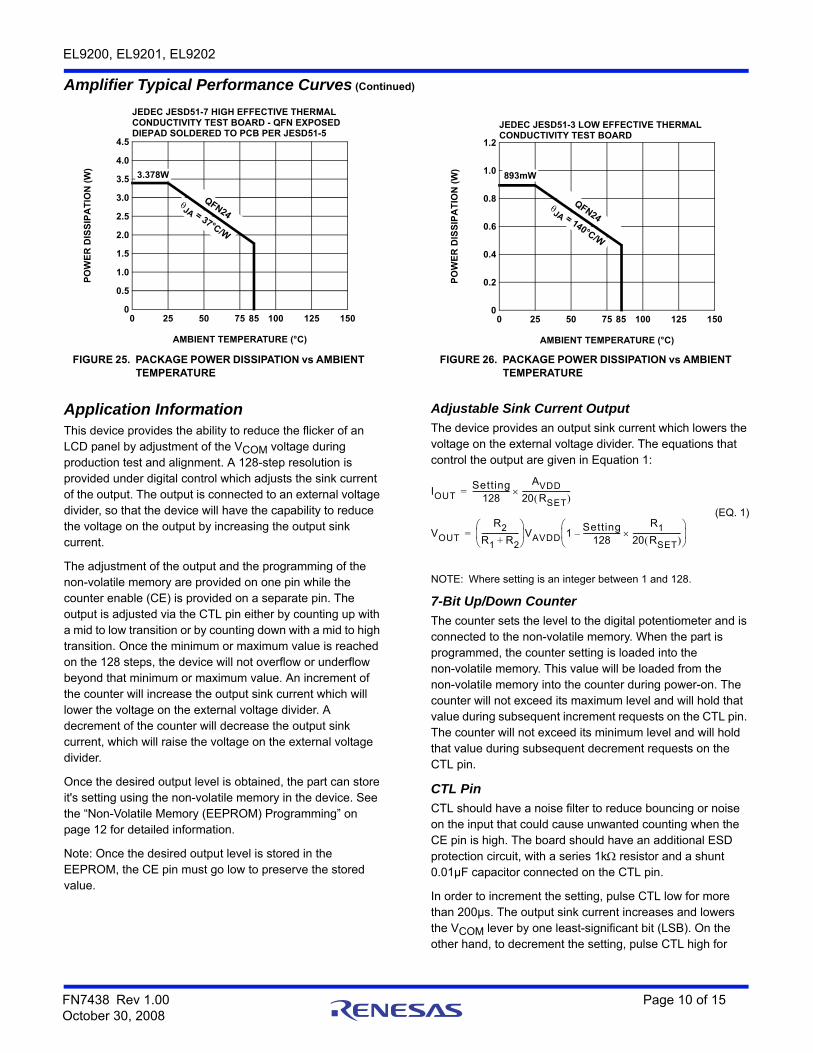
FIGURE 25. PACKAGE POWER DISSIPATION vs AMBIENT TEMPERATURE
FIGURE 26. PACKAGE POWER DISSIPATION vs AMBIENT TEMPERATURE
Amplifier Typical Performance Curves (Continued)
JEDEC JESD51-7 HIGH EFFECTIVE THERMAL CONDUCTIVITY TEST BOARD - QFN EXPOSED DIEPAD SOLDERED TO PCB PER JESD51-5
3.378W
JA = 37°C/W
QFN24
0 150
AMBIENT TEMPERATURE (°C)
75
PO
WE
R D
ISS
IPA
TIO
N (
W)
4.5
3.0
0
1.0
4.0
2.0
2.5
0.5
3.5
1.5
25 10050 12585
JEDEC JESD51-3 LOW EFFECTIVE THERMAL CONDUCTIVITY TEST BOARD
JA = 140°C/W
QFN24
893mW
0 150
AMBIENT TEMPERATURE (°C)
75
PO
WE
R D
ISS
IPA
TIO
N (
W)
1.2
0.6
0
1.0
0.2
0.4
0.8
25 10050 12585
IOUTSetting
128---------------------
AVDD20 RSET ---------------------------=
VOUT
R2R1 R2+---------------------
VAVDD 1Setting
128---------------------
R120 RSET ---------------------------–
=
(EQ. 1)
FN7438 Rev 1.00 Page 10 of 15October 30, 2008
EL9200, EL9201, EL9202
more than 200µs. The output sink current will decrease and the VCOM level will increase by one LSB.
To avoid unintentional adjustment, the EL9200, EL9201, and EL9202 guarantees to reject CTL pulses shorter than 20µs.
Since the internal comparators come up in an unknown state, the very first CTL pulse is ignored to avoid the possibility of a false pulse.
See Figure 27 for the timing information.
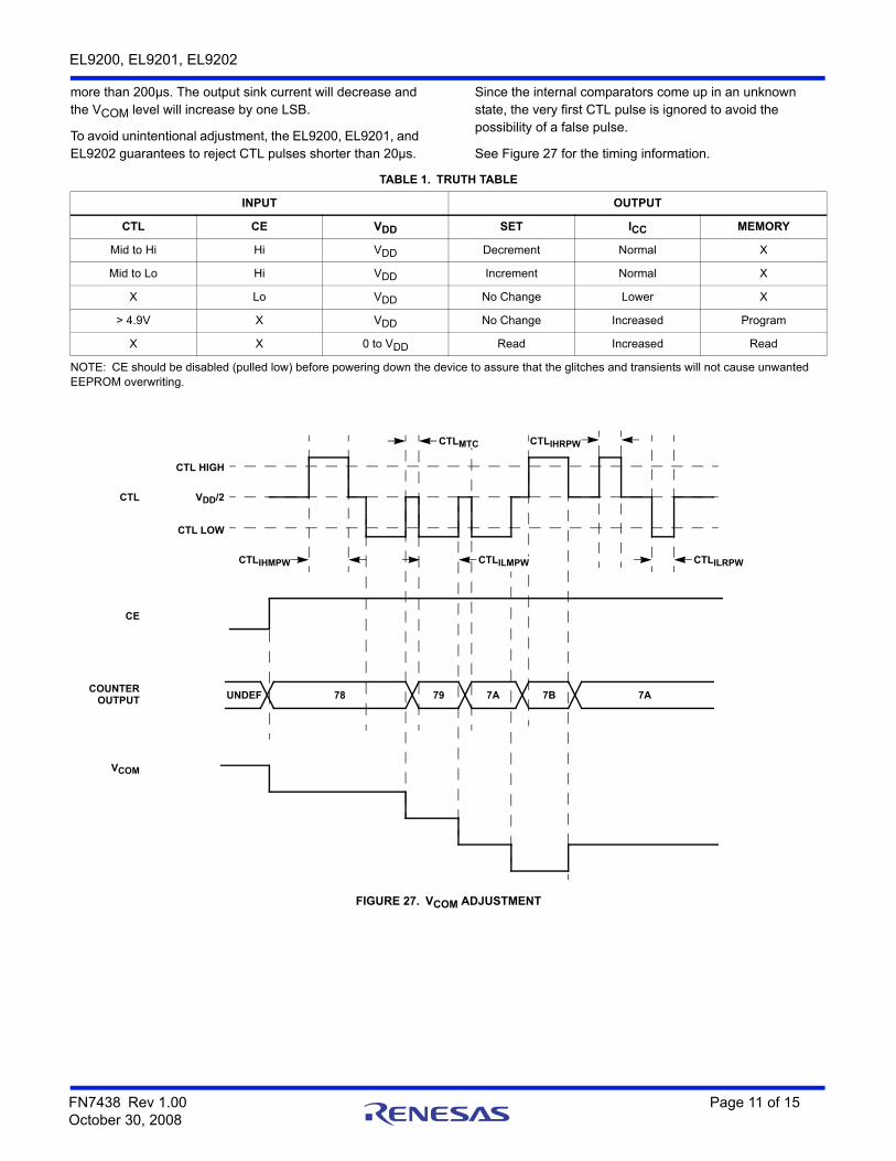
FIGURE 27. VCOM ADJUSTMENT
TABLE 1. TRUTH TABLE
INPUT OUTPUT
CTL CE VDD SET ICC MEMORY
Mid to Hi Hi VDD Decrement Normal X
Mid to Lo Hi VDD Increment Normal X
X Lo VDD No Change Lower X
> 4.9V X VDD No Change Increased Program
X X 0 to VDD Read Increased Read
NOTE: CE should be disabled (pulled low) before powering down the device to assure that the glitches and transients will not cause unwanted EEPROM overwriting.
CTL HIGH
VDD/2
CTL LOW
78 79 7A 7B 7AUNDEF
CTLIHMPW CTLILRPWCTLILMPW
CTLMTC CTLIHRPW
CTL
CE
COUNTEROUTPUT
VCOM
FN7438 Rev 1.00 Page 11 of 15October 30, 2008
EL9200, EL9201, EL9202
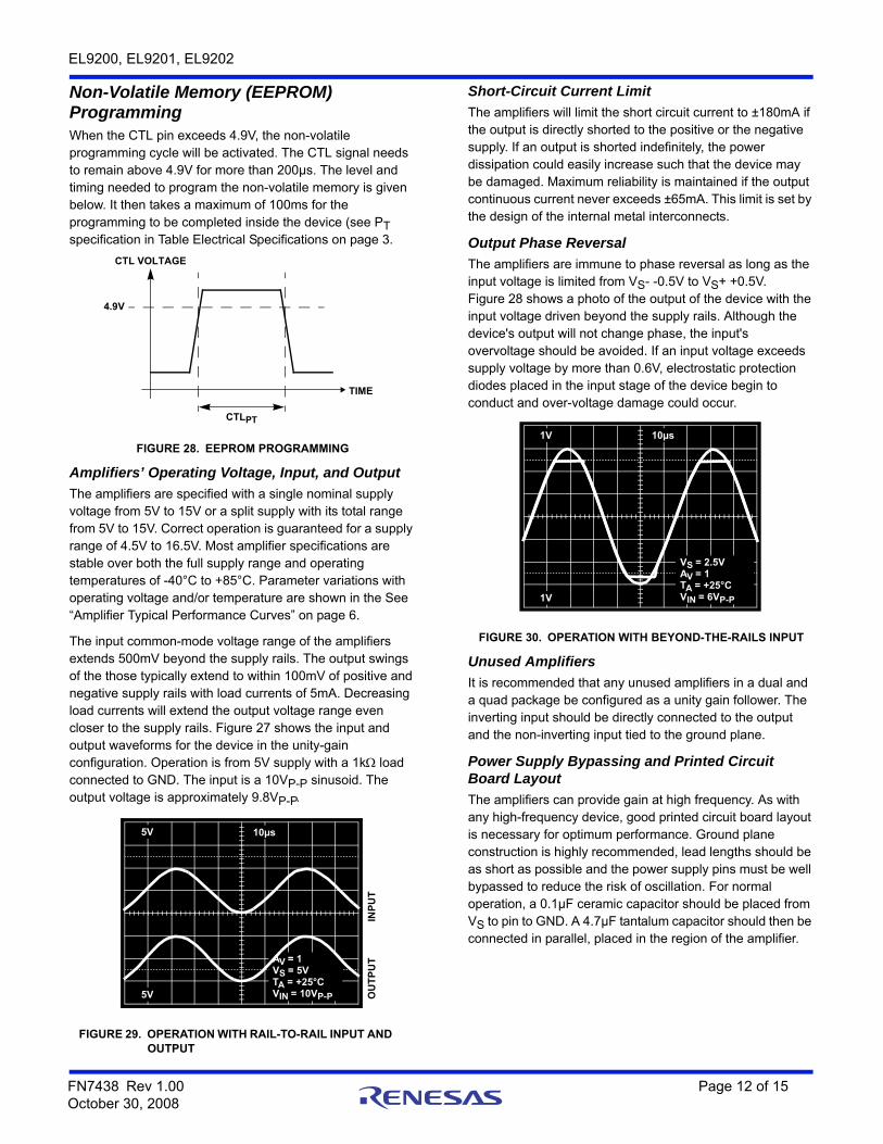
Non-Volatile Memory (EEPROM) ProgrammingWhen the CTL pin exceeds 4.9V, the non-volatile programming cycle will be activated. The CTL signal needs to remain above 4.9V for more than 200µs. The level and timing needed to program the non-volatile memory is given below. It then takes a maximum of 100ms for the programming to be completed inside the device (see PT specification in Table Electrical Specifications on page 3.
FIGURE 28. EEPROM PROGRAMMING
Amplifiers’ Operating Voltage, Input, and Output
The amplifiers are specified with a single nominal supply voltage from 5V to 15V or a split supply with its total range from 5V to 15V. Correct operation is guaranteed for a supply range of 4.5V to 16.5V. Most amplifier specifications are stable over both the full supply range and operating temperatures of -40°C to +85°C. Parameter variations with operating voltage and/or temperature are shown in the See “Amplifier Typical Performance Curves” on page 6.
The input common-mode voltage range of the amplifiers extends 500mV beyond the supply rails. The output swings of the those typically extend to within 100mV of positive and negative supply rails with load currents of 5mA. Decreasing load currents will extend the output voltage range even closer to the supply rails. Figure 27 shows the input and output waveforms for the device in the unity-gain configuration. Operation is from 5V supply with a 1k load connected to GND. The input is a 10VP-P sinusoid. The output voltage is approximately 9.8VP-P.
FIGURE 29. OPERATION WITH RAIL-TO-RAIL INPUT AND OUTPUT
Short-Circuit Current Limit
The amplifiers will limit the short circuit current to ±180mA if the output is directly shorted to the positive or the negative supply. If an output is shorted indefinitely, the power dissipation could easily increase such that the device may be damaged. Maximum reliability is maintained if the output continuous current never exceeds ±65mA. This limit is set by the design of the internal metal interconnects.
Output Phase Reversal
The amplifiers are immune to phase reversal as long as the input voltage is limited from VS- -0.5V to VS+ +0.5V.Figure 28 shows a photo of the output of the device with the input voltage driven beyond the supply rails. Although the device's output will not change phase, the input's overvoltage should be avoided. If an input voltage exceeds supply voltage by more than 0.6V, electrostatic protection diodes placed in the input stage of the device begin to conduct and over-voltage damage could occur.
FIGURE 30. OPERATION WITH BEYOND-THE-RAILS INPUT
Unused Amplifiers
It is recommended that any unused amplifiers in a dual and a quad package be configured as a unity gain follower. The inverting input should be directly connected to the output and the non-inverting input tied to the ground plane.
Power Supply Bypassing and Printed Circuit Board Layout
The amplifiers can provide gain at high frequency. As with any high-frequency device, good printed circuit board layout is necessary for optimum performance. Ground plane construction is highly recommended, lead lengths should be as short as possible and the power supply pins must be well bypassed to reduce the risk of oscillation. For normal operation, a 0.1µF ceramic capacitor should be placed from VS to pin to GND. A 4.7µF tantalum capacitor should then be connected in parallel, placed in the region of the amplifier.
CTLPT
TIME
4.9V
CTL VOLTAGE
OU
TP
UT
INP
UT
5V
5V 10µs
AV = 1VS = 5VTA = +25°CVIN = 10VP-P
1V
1V 10µs
VS = 2.5VAV = 1TA = +25°CVIN = 6VP-P
FN7438 Rev 1.00 Page 12 of 15October 30, 2008
EL9200, EL9201, EL9202
Intersil products are manufactured, assembled and tested utilizing ISO9001 quality systems as notedin the quality certifications found at www.intersil.com/en/support/qualandreliability.html
Intersil products are sold by description only. Intersil may modify the circuit design and/or specifications of products at any time without notice, provided that such modification does not, in Intersil's sole judgment, affect the form, fit or function of the product. Accordingly, the reader is cautioned to verify that datasheets are current before placing orders. Information furnished by Intersil is believed to be accurate and reliable. However, no responsibility is assumed by Intersil or its subsidiaries for its use; nor for any infringements of patents or other rights of third parties which may result from its use. No license is granted by implication or otherwise under any patent or patent rights of Intersil or its subsidiaries.
For information regarding Intersil Corporation and its products, see www.intersil.com
For additional products, see www.intersil.com/en/products.html
© Copyright Intersil Americas LLC 2005-2008. All Rights Reserved.All trademarks and registered trademarks are the property of their respective owners.
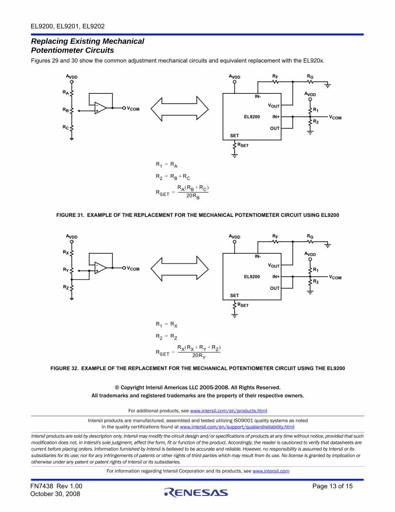
Replacing Existing Mechanical Potentiometer CircuitsFigures 29 and 30 show the common adjustment mechanical circuits and equivalent replacement with the EL920x.
FIGURE 31. EXAMPLE OF THE REPLACEMENT FOR THE MECHANICAL POTENTIOMETER CIRCUIT USING EL9200
FIGURE 32. EXAMPLE OF THE REPLACEMENT FOR THE MECHANICAL POTENTIOMETER CIRCUIT USING THE EL9200
-+
VCOM
RA
RB
RC
AVDD
VOUT
IN+
OUT
EL9200
SET
AVDD
IN-
RF RG
AVDD
R1
R2VCOM
RSET
R1 RA=
R2 RB RC+=
RSET
RA RB RC+
20RB------------------------------------=
-+
VCOM
RX
RY
RZ
AVDD
VOUT
IN+
OUT
EL9200
SET
AVDD
IN-
RF RG
AVDD
R1
R2VCOM
RSET
R1 RX=
R2 RZ=
RSET
RX RX RY RZ+ +
20RY--------------------------------------------------=
FN7438 Rev 1.00 Page 13 of 15October 30, 2008
EL9200, EL9201, EL9202
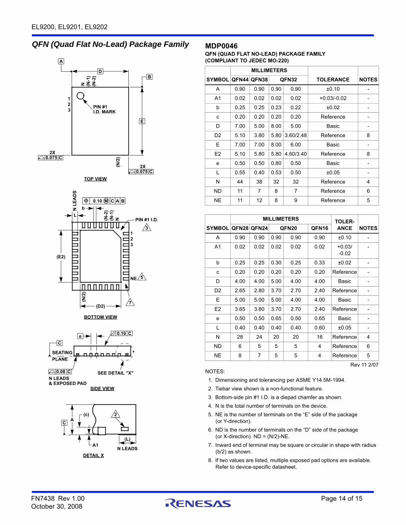
QFN (Quad Flat No-Lead) Package Family
PIN #1I.D. MARK
21
3
(N-2
)(N
-1)
N
(N/2
)
2X0.075
TOP VIEW
(N/2
)
NE
23
1
PIN #1 I.D.(N-2
)(N
-1)
N
b
L
N L
EA
DS
BOTTOM VIEW
DETAIL X
PLANE
SEATING
N LEADS
C
SEE DETAIL "X"
A1(L)
N LEADS
& EXPOSED PAD
0.10
SIDE VIEW
0.10 BAM C
C
B
A
E
2X0.075 C
D
3
5
7
(E2)
(D2)
e
0.08 C
C
(c)A
2
C
MDP0046QFN (QUAD FLAT NO-LEAD) PACKAGE FAMILY(COMPLIANT TO JEDEC MO-220)
SYMBOL
MILLIMETERS
TOLERANCE NOTESQFN44 QFN38 QFN32
A 0.90 0.90 0.90 0.90 ±0.10 -
A1 0.02 0.02 0.02 0.02 +0.03/-0.02 -
b 0.25 0.25 0.23 0.22 ±0.02 -
c 0.20 0.20 0.20 0.20 Reference -
D 7.00 5.00 8.00 5.00 Basic -
D2 5.10 3.80 5.80 3.60/2.48 Reference 8
E 7.00 7.00 8.00 6.00 Basic -
E2 5.10 5.80 5.80 4.60/3.40 Reference 8
e 0.50 0.50 0.80 0.50 Basic -
L 0.55 0.40 0.53 0.50 ±0.05 -
N 44 38 32 32 Reference 4
ND 11 7 8 7 Reference 6
NE 11 12 8 9 Reference 5
SYMBOL
MILLIMETERS TOLER-ANCE NOTESQFN28 QFN24 QFN20 QFN16
A 0.90 0.90 0.90 0.90 0.90 ±0.10 -
A1 0.02 0.02 0.02 0.02 0.02 +0.03/-0.02
-
b 0.25 0.25 0.30 0.25 0.33 ±0.02 -
c 0.20 0.20 0.20 0.20 0.20 Reference -
D 4.00 4.00 5.00 4.00 4.00 Basic -
D2 2.65 2.80 3.70 2.70 2.40 Reference -
E 5.00 5.00 5.00 4.00 4.00 Basic -
E2 3.65 3.80 3.70 2.70 2.40 Reference -
e 0.50 0.50 0.65 0.50 0.65 Basic -
L 0.40 0.40 0.40 0.40 0.60 ±0.05 -
N 28 24 20 20 16 Reference 4
ND 6 5 5 5 4 Reference 6
NE 8 7 5 5 4 Reference 5
Rev 11 2/07NOTES:
1. Dimensioning and tolerancing per ASME Y14.5M-1994.
2. Tiebar view shown is a non-functional feature.
3. Bottom-side pin #1 I.D. is a diepad chamfer as shown.
4. N is the total number of terminals on the device.
5. NE is the number of terminals on the “E” side of the package(or Y-direction).
6. ND is the number of terminals on the “D” side of the package(or X-direction). ND = (N/2)-NE.
7. Inward end of terminal may be square or circular in shape with radius (b/2) as shown.
8. If two values are listed, multiple exposed pad options are available. Refer to device-specific datasheet.
FN7438 Rev 1.00 Page 14 of 15October 30, 2008
EL9200, EL9201, EL9202
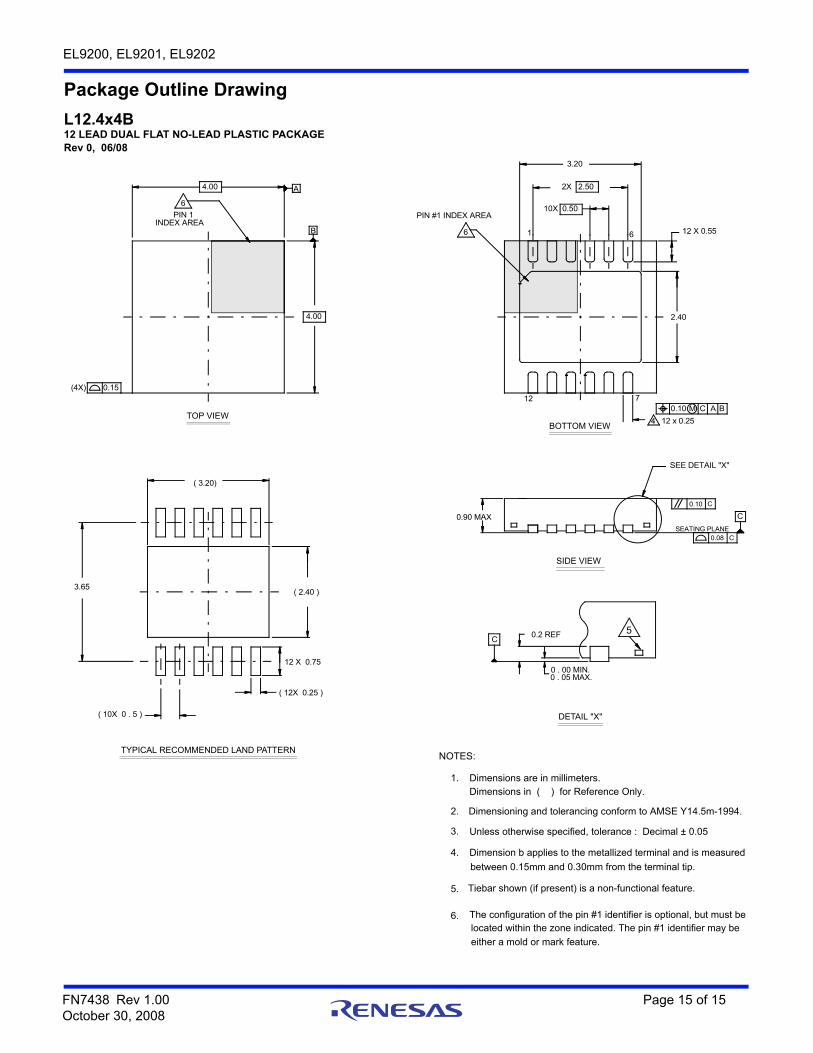
Package Outline Drawing
L12.4x4B12 LEAD DUAL FLAT NO-LEAD PLASTIC PACKAGERev 0, 06/08
TYPICAL RECOMMENDED LAND PATTERN
DETAIL "X"
TOP VIEWBOTTOM VIEW
SIDE VIEW
located within the zone indicated. The pin #1 identifier may be
Unless otherwise specified, tolerance : Decimal ± 0.05
Tiebar shown (if present) is a non-functional feature.
The configuration of the pin #1 identifier is optional, but must be
between 0.15mm and 0.30mm from the terminal tip.
Dimension b applies to the metallized terminal and is measured
Dimensions in ( ) for Reference Only.
Dimensioning and tolerancing conform to AMSE Y14.5m-1994.
6.
either a mold or mark feature.
3.
5.
4.
2.
Dimensions are in millimeters.1.
NOTES:
(4X) 0.15
4.00
INDEX AREA
6
PIN 1
4.00
B
A
2.40
12 X 0.55
120.10
12 x 0.25 4
7A BCM
PIN #1 INDEX AREA
6 1
2X 2.50
6
10X 0.50
3.20
0.90 MAX
SEE DETAIL "X"
C
SEATING PLANE0.08 C
0.10 C
( 3.20)
3.65
( 10X 0 . 5 )
( 12X 0.25 )
( 2.40 )
12 X 0.75
0.2 REFC
0 . 05 MAX.0 . 00 MIN.
5
FN7438 Rev 1.00 Page 15 of 15October 30, 2008