elen0037 microelectronic ic design · – using mosfet, one can realize switches with low losses...
TRANSCRIPT

ELEN0037 Microelectronic IC Design
Prof. Dr. Michael Kraft
Lecture 2: Technological Aspects
Technology – Passive components – Active components – CMOS Process
Basic Layout Scaling
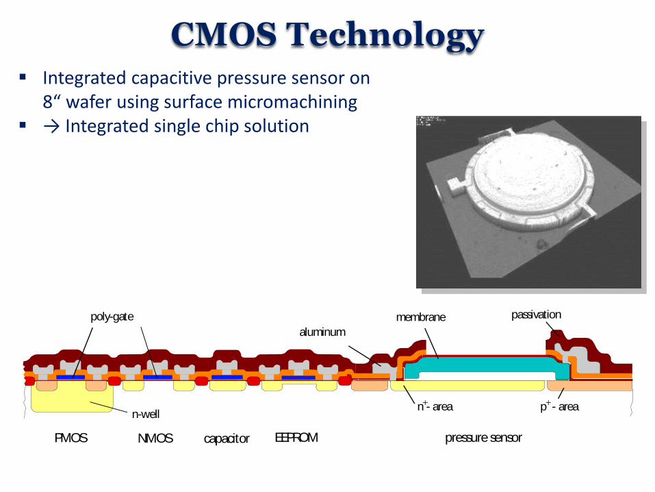
CMOS Technology Integrated capacitive pressure sensor on
8“ wafer using surface micromachining → Integrated single chip solution
aluminum
n - area+
membrane
p - area
passivation
+
PMOS NMOS capacitor EEPROM pressure sensor
poly-gate
n-well

Passive Components Passive components:
– Resistors • Diffused/implanted resistors • Polysilicon resistors
– Capacitors
n+ diffusion resistor Source: Allen, Holberg, „CMOS Analog Circuit Design“
Aluminium
SiO 2 n +
p - Substrate

Fabrication n+ Diffusion Resistor
Aluminium
SiO2 n+
p-Substrate
p - Substrate
p - Substrate
p - Substrate
n+
n+
n+ - Implantation
Etch holes Oxide
Aluminium
Fabrication process Mask layout
Diffusion Resistor: – Source/Drain
diffusion
n+ Diffusion Resistor
Aluminium
SiO2 n+
p-Substrate A
L
Xj
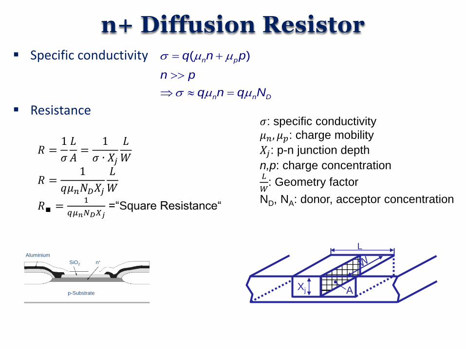
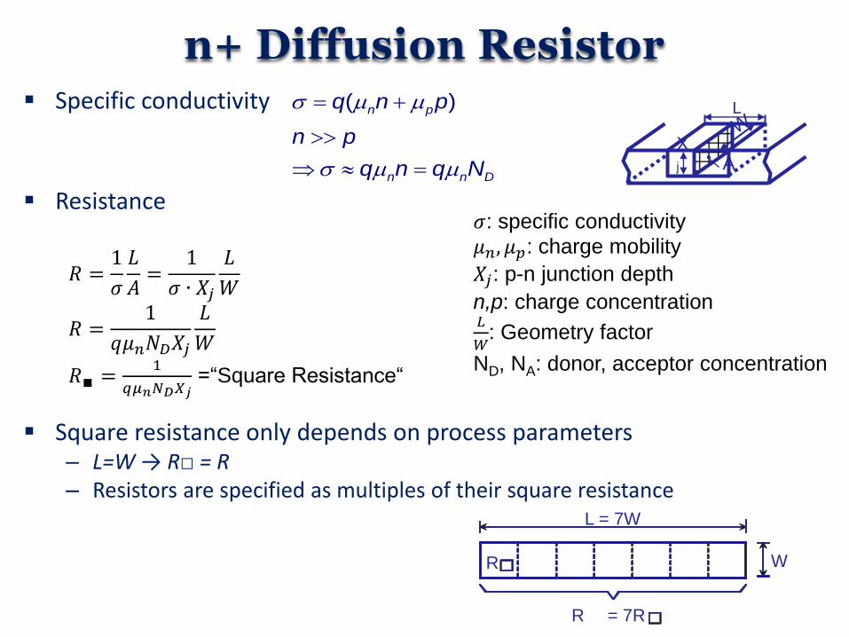
Specific conductivity
( )n p
n n D
q n p
n p
q n q N
Resistance
𝑅 =1
𝜎
𝐿
𝐴=
1
𝜎 ∙ 𝑋𝑗
𝐿
𝑊
𝑅 =1
𝑞𝜇𝑛𝑁𝐷𝑋𝑗
𝐿
𝑊
𝑅∎ =1
𝑞𝜇𝑛𝑁𝐷𝑋𝑗 =“Square Resistance“
𝜎: specific conductivity
𝜇𝑛, 𝜇𝑝: charge mobility
𝑋𝑗: p-n junction depth
n,p: charge concentration 𝐿
𝑊: Geometry factor
ND, NA: donor, acceptor concentration
n+ Diffusion Resistor
A
L
Xj
Specific conductivity
( )n p
n n D
q n p
n p
q n q N
Resistance
𝑅 =1
𝜎
𝐿
𝐴=
1
𝜎 ∙ 𝑋𝑗
𝐿
𝑊
𝑅 =1
𝑞𝜇𝑛𝑁𝐷𝑋𝑗
𝐿
𝑊
𝑅∎ =1
𝑞𝜇𝑛𝑁𝐷𝑋𝑗 =“Square Resistance“
𝜎: specific conductivity
𝜇𝑛, 𝜇𝑝: charge mobility
𝑋𝑗: p-n junction depth
n,p: charge concentration 𝐿
𝑊: Geometry factor
ND, NA: donor, acceptor concentration
Square resistance only depends on process parameters – L=W → R□ = R – Resistors are specified as multiples of their square resistance
L = 7W
R W
R = 7R
n+ Diffusion Resistor
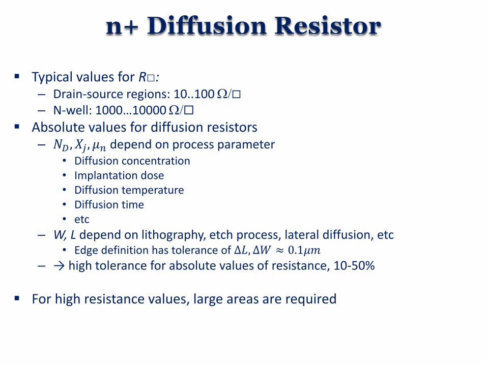
Typical values for R□: – Drain-source regions: 10..100 W/
– N-well: 1000…10000 W/
Absolute values for diffusion resistors – 𝑁𝐷, 𝑋𝑗 , 𝜇𝑛 depend on process parameter
• Diffusion concentration • Implantation dose • Diffusion temperature • Diffusion time • etc
– W, L depend on lithography, etch process, lateral diffusion, etc • Edge definition has tolerance of Δ𝐿, Δ𝑊 ≈ 0.1𝜇𝑚
– → high tolerance for absolute values of resistance, 10-50%
For high resistance values, large areas are required
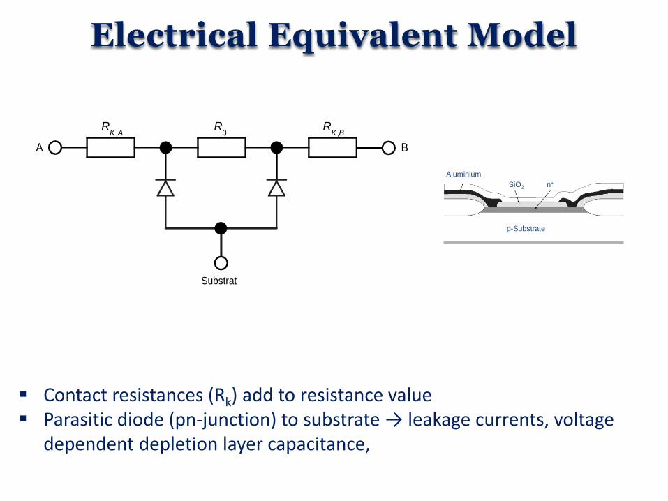
Electrical Equivalent Model
Contact resistances (Rk) add to resistance value Parasitic diode (pn-junction) to substrate → leakage currents, voltage
dependent depletion layer capacitance,
Substrat
AKR
, 0R
BKR
,
A B
Aluminium
SiO2 n+
p-Substrate
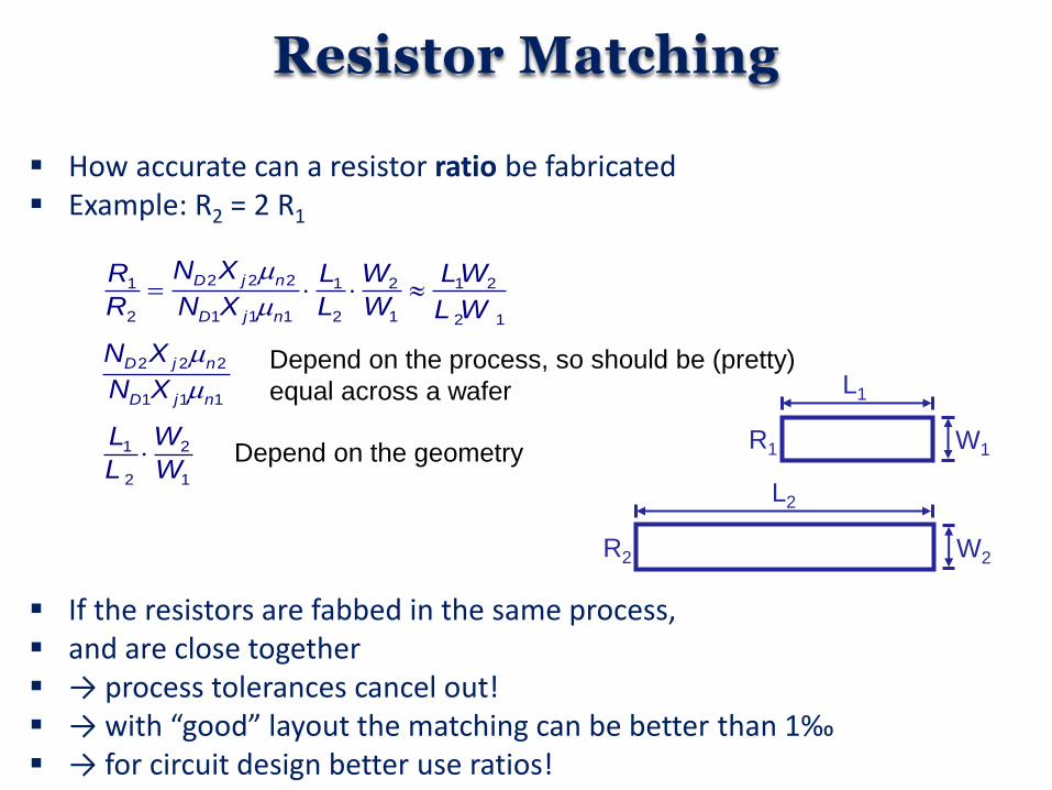
Resistor Matching
How accurate can a resistor ratio be fabricated Example: R2 = 2 R1
2 2 21 1 2 1 2
2 1 1 1 2 1 2 1
D j n
D j n
N XR L W LW
R N X L W L W
2 2 2
1 1 1
D j n
D j n
N X
N X
Depend on the process, so should be (pretty)
equal across a wafer
1 2
2 1
L W
L W Depend on the geometry
L1
R1 W1
R2 W2
L2
If the resistors are fabbed in the same process, and are close together → process tolerances cancel out! → with “good” layout the matching can be better than 1‰ → for circuit design better use ratios!
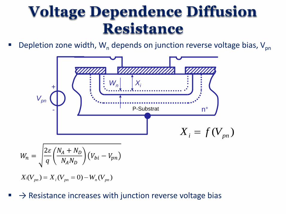
Voltage Dependence Diffusion Resistance
Depletion zone width, Wn depends on junction reverse voltage bias, Vpn
P-Substrat
Vpn
Xi Wn
n+
+
-
→ Resistance increases with junction reverse voltage bias
𝑊𝑛 =2𝜀
𝑞
𝑁𝐴 +𝑁𝐷𝑁𝐴𝑁𝐷
𝑉𝑏𝑖 − 𝑉𝑝𝑛
)( pni VfX
)()0()( pnnpnipni VWVXVX
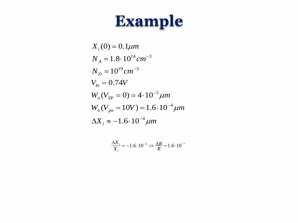
Example
mX
mVVW
mVW
VV
cmN
cmN
mX
i
pnn
SPn
bi
D
A
i
4
4
5
319
314
106.1
106.1)10(
104)0(
74.0
10
108.1
1.0)0(
3
106.1106.1 3
RR
X
X
i
i

Voltage Coefficient Diffusion Resistance
VppmVVR
R/160106.11 14
Voltage dependency increases with: – Lower doping – Higher square resistance – Thinner layers
Typical values – n+ implantation: 20 W/ 100ppm/V – p+ implantation: 100 W/ 1100ppm/V – n- Implantation: 8 kW/ 20000 ppm/V
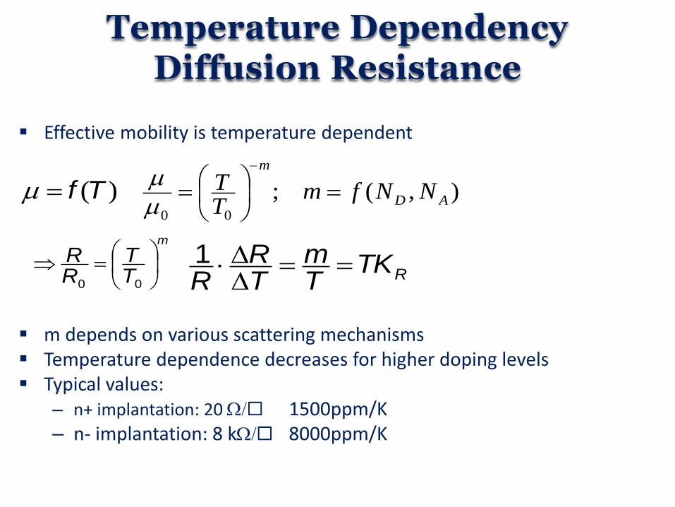
Temperature Dependency Diffusion Resistance
Effective mobility is temperature dependent
)(Tf ),(;00
AD
m
NNfmTT
m
TT
RR
00RTK
Tm
TR
R
1
m depends on various scattering mechanisms Temperature dependence decreases for higher doping levels Typical values:
– n+ implantation: 20 W/ 1500ppm/K – n- implantation: 8 kW/ 8000ppm/K
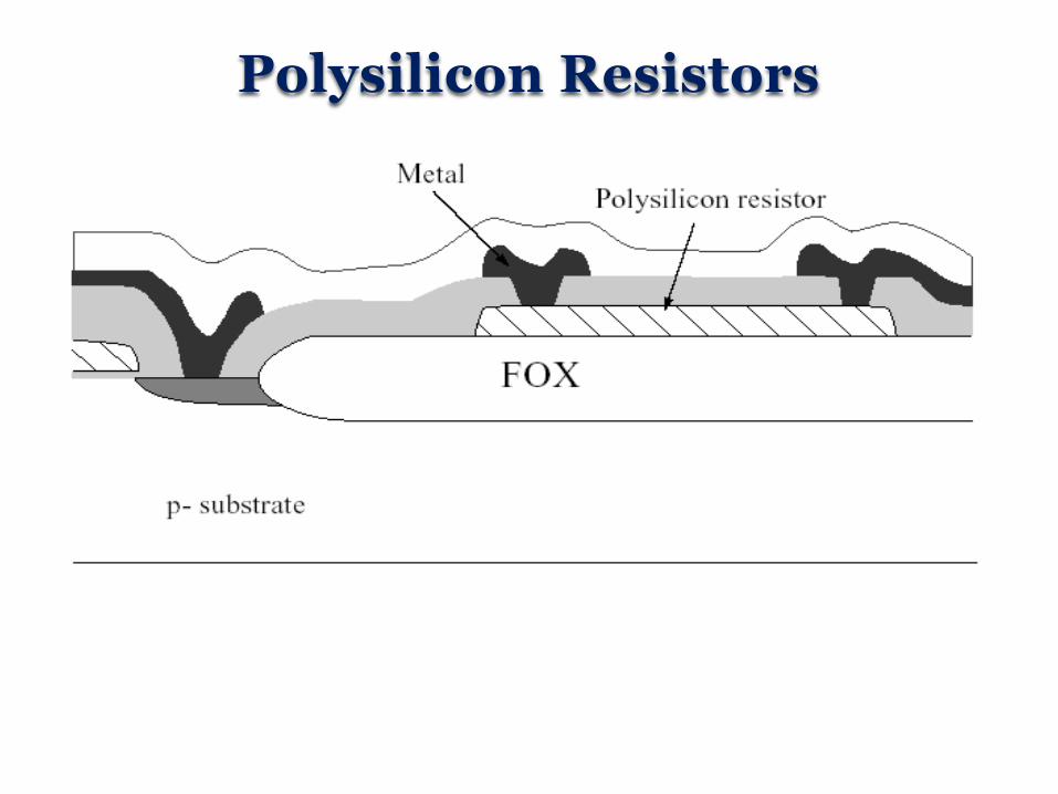
Polysilicon Resistors
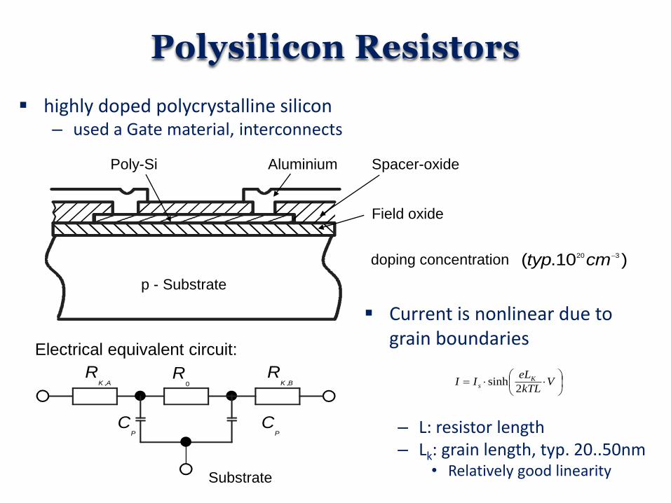
Polysilicon Resistors
highly doped polycrystalline silicon – used a Gate material, interconnects
p - Substrate
Poly-Si Aluminium Spacer-oxide
Field oxide
doping concentration )10.( 320 cmtyp
Electrical equivalent circuit:
AKR
, 0R
BKR
,
Substrate
PC
PC
Current is nonlinear due to grain boundaries
V
kTL
eLII K
s 2sinh
– L: resistor length – Lk: grain length, typ. 20..50nm
• Relatively good linearity
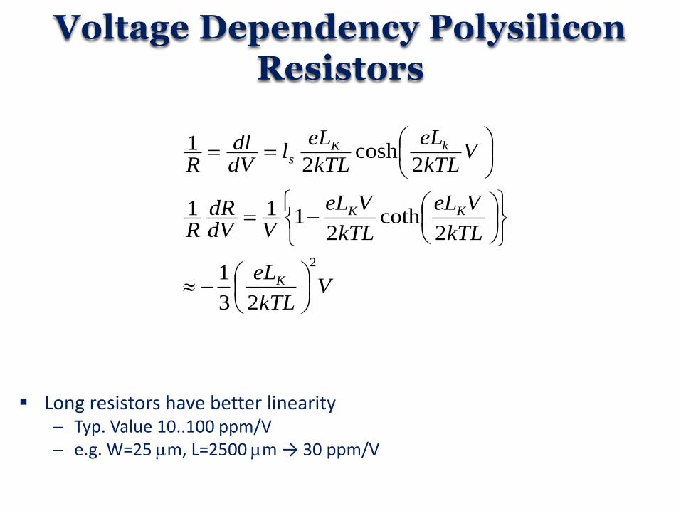
Voltage Dependency Polysilicon Resistors
Long resistors have better linearity – Typ. Value 10..100 ppm/V – e.g. W=25 m, L=2500 m → 30 ppm/V
VkTL
eL
kTL
VeL
kTL
VeL
VdVdR
R
VkTL
eL
kTL
eLl
dVdl
R
K
KK
kKs
2
23
1
2coth
2111
2cosh
21

Temperature Dependency Polysilicon Resistors
Long resistors have lower temperature dependency – Typ. Value 100..500 ppm/K – e.g. L=300 m, V=2 V → 200 ppm/K
2
23
1
2coth
21
11
kTL
VeL
T
kTL
VeL
kTL
VeL
TdT
dR
R
K
KK

Capacitors
CMOS technology: – High quality, thin gate oxide layers are available – Using MOSFET, one can realize switches with low losses – Using MOSFET, one can read-out stored voltages without (almost) losses
p- substrate n+ Implantation
SiO2
Feldoxid Feldoxid
Polysilicon Alu Gate SiO2
Field oxide Field oxide
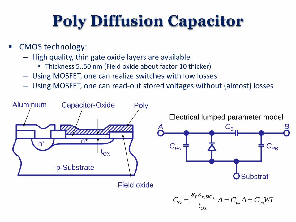
Poly Diffusion Capacitor
CMOS technology: – High quality, thin gate oxide layers are available
• Thickness 5..50 nm (Field oxide about factor 10 thicker)
– Using MOSFET, one can realize switches with low losses – Using MOSFET, one can read-out stored voltages without (almost) losses
Capacitor-Oxide Aluminium Poly
Field oxide
p-Substrate
n+ n+
tOX
A B C0
CPB CPA
Substrat
Electrical lumped parameter model
WLCACAt
C oxox
OX
SiOr
O 2,0

Poly Diffusion Capacitor
C* depends on the process only – Typical values 500 pF/mm2 .. 1.5 nF/mm2
Small temperature and voltage dependency Absolute accuracy 10%..20% Matched pairs accuracy < 0.1% Disadvantage: diode to substrate
Capacitor-Oxide Aluminium Poly
Field oxide
p-Substrate
n+ n+
tOX
VppmdV
dC
C
KppmdT
dC
C
/71
/201
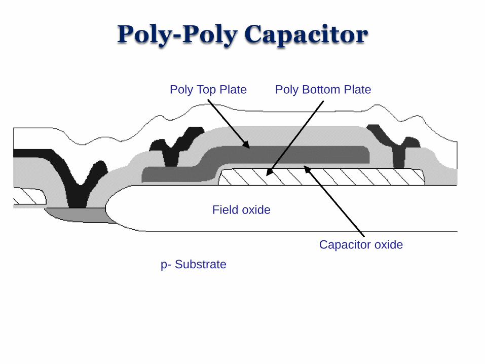
Poly-Poly Capacitor
p- Substrate
Field oxide
Capacitor oxide
Poly Bottom Plate Poly Top Plate
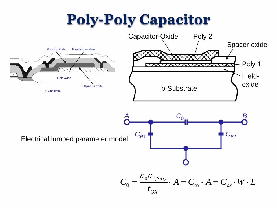
Poly-Poly Capacitor Capacitor-Oxide
p-Substrate
Poly 2
Spacer oxide
Poly 1
Field-
oxide
A B C0
CP2 CP1
LWCACAt
C oxox
OX
Sior 2,0
0
Electrical lumped parameter model

Poly-Poly Capacitor Absolute Value
L
W
2
2
Source of tolerances – 1. Edge uncertainty due to tolerances in
• Lithography • Etching
– → W+ and L+ • Area A = WL, circumference U = 2 (W+L)
A
U
A
AA
UA
UAA
LWWLLWA
2
´
22´
`
2
2
– → minimal error for minimum ratio U to A • → quadratic layout (best spherical)
– 2. oxide thickness • Process dependent
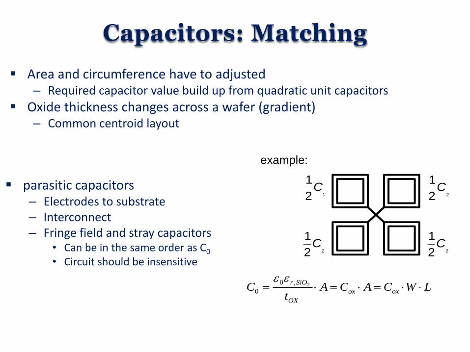
Capacitors: Matching
Area and circumference have to adjusted – Required capacitor value build up from quadratic unit capacitors
Oxide thickness changes across a wafer (gradient) – Common centroid layout
parasitic capacitors – Electrodes to substrate – Interconnect – Fringe field and stray capacitors
• Can be in the same order as C0
• Circuit should be insensitive
LWCACA
tC oxox
OX
SiOr 2,0
0
example:
12
1C
22
1C
22
1C
22
1C
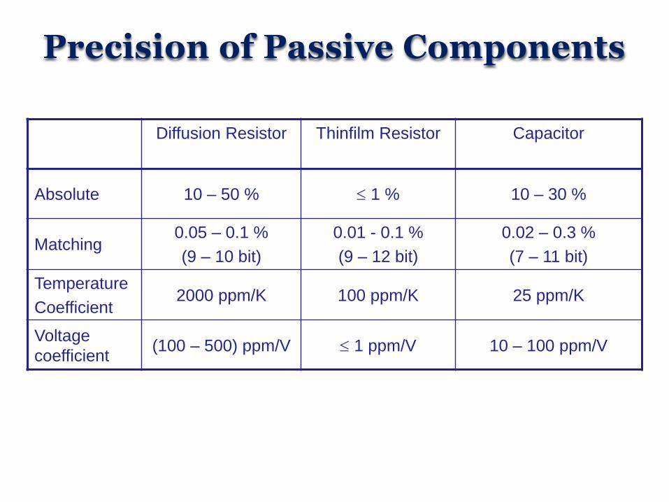
Precision of Passive Components
Diffusion Resistor Thinfilm Resistor Capacitor
Absolute 10 – 50 % 1 % 10 – 30 %
Matching 0.05 – 0.1 %
(9 – 10 bit)
0.01 - 0.1 %
(9 – 12 bit)
0.02 – 0.3 %
(7 – 11 bit)
Temperature
Coefficient 2000 ppm/K 100 ppm/K 25 ppm/K
Voltage
coefficient (100 – 500) ppm/V 1 ppm/V 10 – 100 ppm/V

MOSFET Fabrication
b) Aktive areas
n - Wanne n - well
Feldoxid Field oxide
a) n - well
n -
p - substrate
Well oxide
n - well
p -
n - well
p - substrate
Field oxide Gate oxide
n -
p -
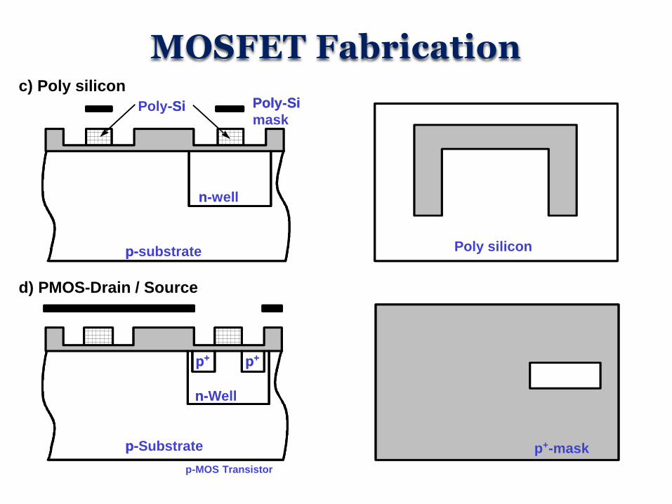
MOSFET Fabrication c) Poly silicon
Polysilizium Poly silicon
p + - Maske p + - mask
p - MOS Transistor
d) PMOS - Drain / Source
n - Well
p - Substrate
p + p +
n -
p -
p + p +
n - well
p - substrate
Poly - Si
mask Poly - Si
n -
p -
Poly - Si - Si
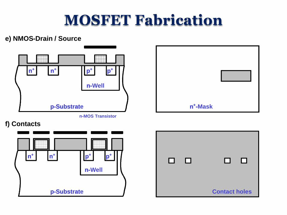
MOSFET Fabrication e) NMOS - Drain / Source
f) Contacts
n + - n + - Mask
Kontaktl ö cher Contact holes
n - Well
p - Substrat
p + p + n + n +
n -
p - Substrate
p + p + n + n +
n - Well
p - Substrat
p + p + n + n +
n -
p - Substrate
p + p + n + n +
n - MOS Transistor
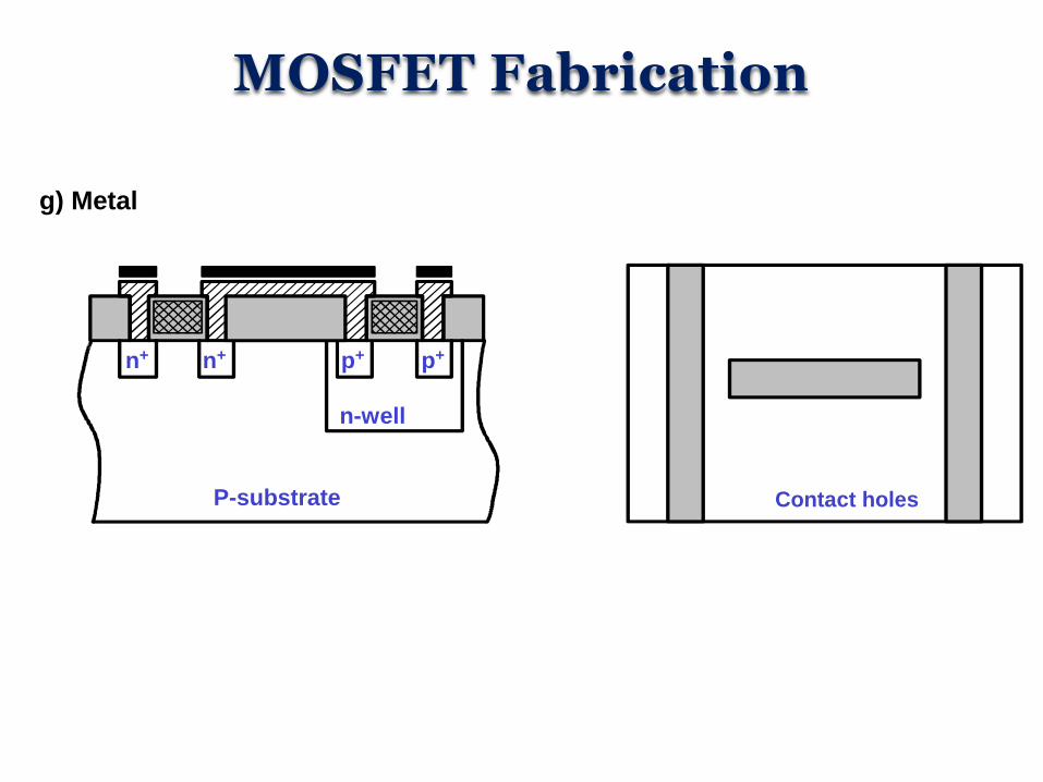
MOSFET Fabrication
g) Metal
n-well
P-substrate
p + p + n + n +
Contact holes

MOSFET Structure
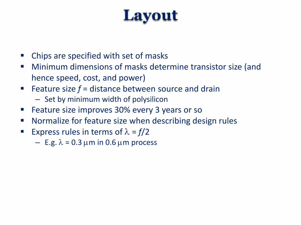
Layout
Chips are specified with set of masks Minimum dimensions of masks determine transistor size (and
hence speed, cost, and power) Feature size f = distance between source and drain
– Set by minimum width of polysilicon
Feature size improves 30% every 3 years or so Normalize for feature size when describing design rules Express rules in terms of l = f/2
– E.g. l = 0.3 m in 0.6 m process

Layout Design Rules
Design Rules Summary
Metal and diffusion have minimum width and spacing of 4l Contacts are 2l x 2l and must be surrounded by 1l on the layers
above and below Polysilicon uses a width of 2l Polysilicon overlaps diffusions by 2l where a transistor is desired and
has spacing or 1l away where no transistor is desired Polysilicon and contacts have a spacing of 3l from other polysilicon
or contacts N-well surrounds pMOS transistors by 6l and avoid nMOS transistors
by 6l
Gate Layout
Layout can be very time consuming – Design gates to fit together nicely – Build a library of standard cells
Standard cell design methodology – VDD and GND should abut (standard height) – Adjacent gates should satisfy design rules – nMOS at bottom and pMOS at top – All gates include well and substrate contacts

Inverter Layout
Transistor dimensions specified as W / L ratio Minimum size is 4l / 2l, sometimes called 1 unit In f = 0.6 m process, this is 1.2 m wide, 0.6 m
long
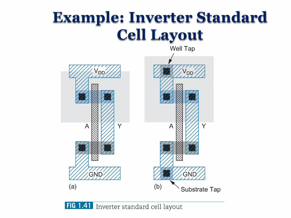
Example: Inverter Standard Cell Layout
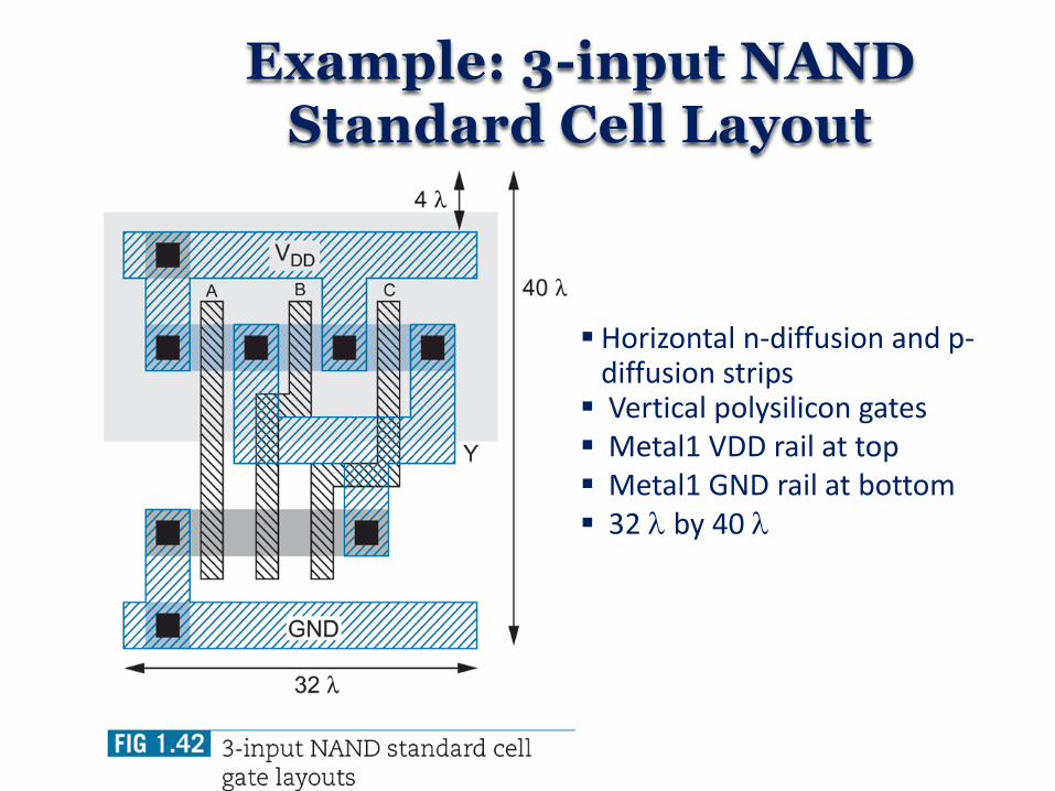
Example: 3-input NAND Standard Cell Layout
Horizontal n-diffusion and p-diffusion strips
Vertical polysilicon gates Metal1 VDD rail at top Metal1 GND rail at bottom 32 l by 40 l

Stick Diagrams
Stick diagrams help plan layout quickly – Need not be to scale – Draw with color pencils or dry-erase markers
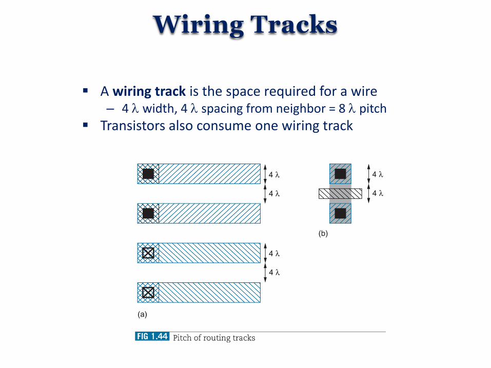
Wiring Tracks
A wiring track is the space required for a wire – 4 l width, 4 l spacing from neighbor = 8 l pitch
Transistors also consume one wiring track
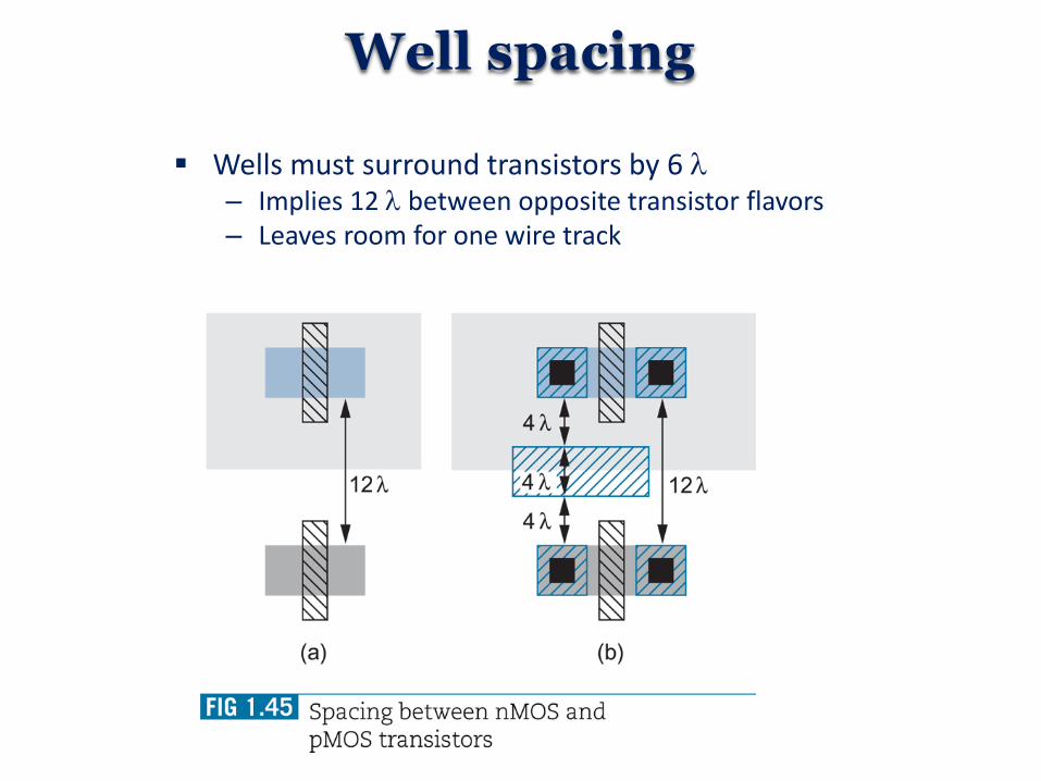
Well spacing
Wells must surround transistors by 6 l – Implies 12 l between opposite transistor flavors – Leaves room for one wire track

Area Estimation
Estimate area by counting wiring tracks – Multiply by 8 to express in l

Scaling The simplest and most common scaling approach is constant field
scaling. The dimensions are scaled in the horizontal & vertical directions, and proportionally increasing the substrate doping by a
factor l, to keep the electric field distribution unchanged. One of the major changes in a short-channel device is that electric
field in the channel region becomes two-dimensional due to the influence of the drain potential.
The substrate doping has to be increased to decrease the depletion width (following from Poisson’s equation).
Small transistors have various undesired effects such as gate oxide degeneration due to ‘hot’ electrons, threshold voltage shift, gate-induced drain leakage, drain-induced barrier lowering (DIBL).
Changes in the fabrication flow have to be introduced to mitigate these unwanted effects, and keep short-channel devices operational.
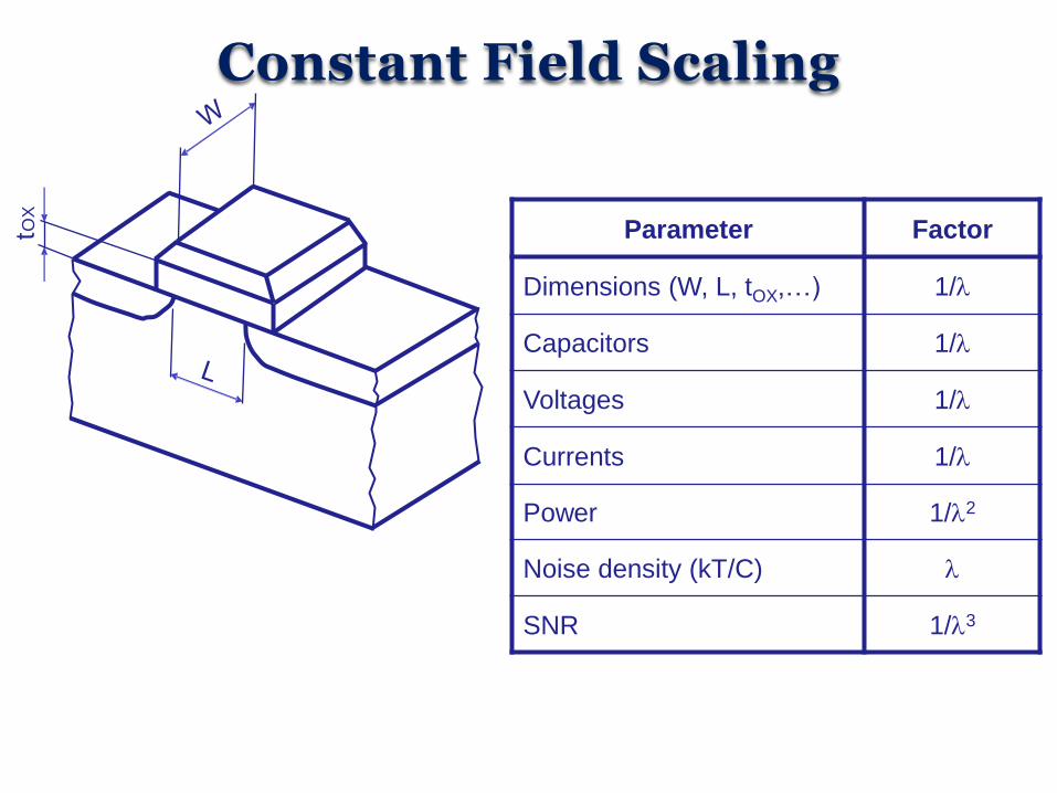
Constant Field Scaling
Parameter Factor
Dimensions (W, L, tOX,…) 1/l
Capacitors 1/l
Voltages 1/l
Currents 1/l
Power 1/l2
Noise density (kT/C) l
SNR 1/l3
t OX
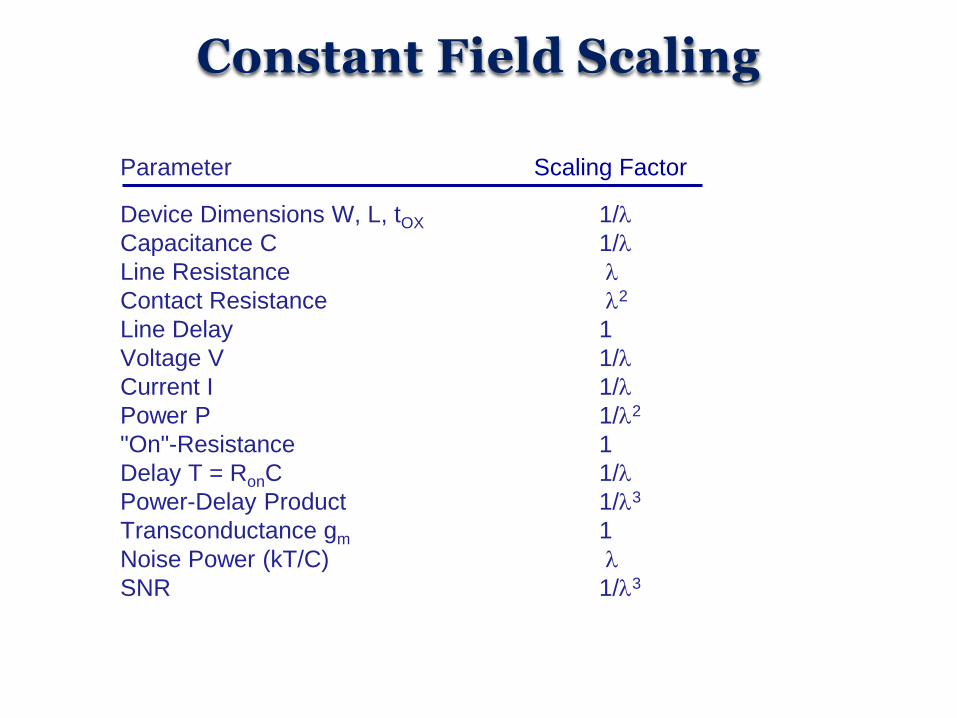
Constant Field Scaling
Device Dimensions W, L, tOX 1/l
Capacitance C 1/l
Line Resistance l
Contact Resistance l2
Line Delay 1
Voltage V 1/l
Current I 1/l
Power P 1/l2
"On"-Resistance 1
Delay T = RonC 1/l
Power-Delay Product 1/l3
Transconductance gm 1
Noise Power (kT/C) l
SNR 1/l3
Parameter Scaling Factor
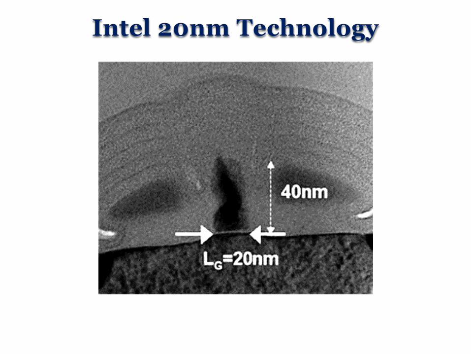
Intel 20nm Technology