eparation of zincpr oxide films by an electrstatic spray...
TRANSCRIPT

Journal of Ceramic Processing Research. Vol. 7, No. 1, pp. 70~74 (2006)
70
J O U R N A L O F
CeramicProcessing Research
Preparation of zinc oxide films by an electrostatic spray deposition process
Ju-Hyun Jeonga,b, Young-Sun Jeona,b, Kyung-Ok Jeona,b, Kyu-Seog Hwanga and Byung-Hoon Kimb,*
aDepartment of Applied Optics and Institute of Photoelectronic Technology, 864-1 Wolgye-dong, Gwangsan-gu, Gwangju 506-
824, KoreabDepartment of Materials Science & Engineering, Chonnam National University, 300 Yongbong-dong, Buk-gu, Gwangju 500-
757, Korea
Highly transparent ZnO thin films were made by electrostatic spray deposition for 60 minutes-120 minutes at 400 oC on soda-lime-silica slide glass substrates. The peaks in the X-ray diffraction analysis could be indexed as from the structure ofcrystalline zinc oxide. From surface observations using a field emission scanning electron microscope and scanning probemicroscope, the surface morphology of the films was found to depend chiefly on depositing time. All the films exhibit a hightransmittance (> 80%) in the visible region, except for the film deposited for 120 minutes. The band gap values of the ZnOfilms deposited for various time are found to be 3.25-3.27 eV.
Key words: ZnO thin film, Electrostatic spray deposition, Surface morphology, Transmittance.
Introduction
Zinc oxide (ZnO) is an n-type semiconductor with awide band gap of 3.3 eV, showing attractive electricaland optical properties. As a wide band gap material,ZnO has received an increasing amount of attentiondue to its possible applications in ultraviolet (UV)light-emitting devices, electron-acoustic devices, UVdetectors, etc. [1-4]. In recent years, there has beenconsiderable interest in the development of high-qualityZnO films to obtain strong UV emission. Severaltechniques are being used to produce ZnO films; e.g.,chemical vapor deposition, molecular beam epitaxy, radiofrequency magnetron sputtering, and a sol-gel process[5-8].
Electrostatic spray deposition (ESD) [9-10] is capableof dividing a liquid into fairly uniform and well-distri-buted droplets with dimensions that can be controlledfrom several micrometers down to the nanometer range.It has been successfully introduced by Chen et al. as anew film fabrication techniques for ceramic film de-position [11]. Compared with other film fabricationtechniques, ESD offers attractive advantages of easycontrol of film composition, easy control of substratetemperature during deposition, high film growth rate,simple setup, low cost, compatibility with micro-fabri-cation technology and suitability for thick film prepa-ration.
An ESD process makes use of the electrohydro-
dynamic generation and breaking-up of a Taylor coneof a precursor solution at the outlet of a nozzle to forma very fine spray. The spray is then directed at a heatedsubstrate, leading to film deposition. This is differentfrom conventional spray processes, in that the spray inan ESD process consists of mainly charged droplets,which may be monosized when generated [11]. It is apromising route for the synthesis of dense as well asporous thin films at relatively low deposition temper-atures and, thereby, lower materials processing andfabrication costs.
Here, we present the results of ZnO thin films pre-pared by ESD. We investigated crystallinity, surfacemorphology, transmittance in the visible spectra range,and energy band gaps of the films in relation to coatingtime.
Experimental Procedure
A homogeneous precursor solution was prepared bymixing zinc acetate [(CH3COO)2Zn·2H2O] and 2-meth-oxyethanol (HOCH2OCH3). Since zinc acetate has alow solubility in 2-methoxyethanol, 2-aminoethanol(H2HCH2CH2OH) (MEA) was added to obtain a clearsolution (concentration: 0.6 mol zinc acetate/1000 ml2-methoxyethanol). The molar ratio of MEA to zincacetate was fixed at 1.0. The mixing solution wasstirred for 2 h to obtain a homogeneous solution.
Deposition of ZnO films was performed using anESD setup with a vertical configuration. The details ofthe setup used have been reported before [12]. A stain-less steel needle (0.1 mm and 0.23 mm inner and outerdiameter, respectively) was connected to a syringepump (KD200, KD Scientific Inc., U.S.A.) using a
*Corresponding author: Tel : +82-62-530-1711Fax: +82-62-530-1699E-mail: [email protected]

Preparation of zinc oxide films by an electrostatic spray deposition process 71
silicon rubber tube. The flow rate of the precursor solwas kept at 0.2 ml/60 minutes. In order to obtain astable cone-jet mode of electrostatic atomization, ahigh voltage (20 kV) was applied between the needletip and ground electrode using a DC power supply(SHV120-30K-RD, Convertech Co. Ltd., South Korea).Soda-lime-silica glass (SLSG) cleaned in a H2O2 solu-tion, and rinsed in methanol were used as substrates.SLSG substrates on the ground electrode were heatedat 400 oC for 60 minutes, 80 minutes, 100 minutes and120 minutes during spraying. A precursor solution waspumped through the nozzle which was placed 10 cmabove the substrates.
The crystal structure of the coated films was charac-terized by high-resolution X-ray diffraction (HRXRD,X’pert PRO, Philips, Netherlands). The morphology ofthe films was examined by means of a field emissionscanning electron microscope (FE-SEM, S-4700, HitachiCo., Japan). A scanning probe microscope (SPM, XE-200, PSIA, Korea) was adopted to analyze the surfaceroughness of the films. Transmittance in the visiblespectra region was analyzed by ultra violet (UV) spectro-photometer (Cary 500 Scan, Varian Co., Australia).The thickness of the annealed film was approximately0.6-0.7 μm, as determined by observation of fracturecross-sections using a FE-SEM.
Results and Discussion
Figure 1 shows XRD spectra of ZnO films on SLSGsubstrates at 400 oC for 60 minutes-120 minutes. Filmsdeposited at other times reveal the same pattern, exceptfor the intensity between peaks from ZnO, which varydepending on the crystallinity. Broad diffraction peaks
from (100), (002) and (101), corresponding to zincoxide, were observed; accordingly, the diffraction peakscan be indexed in terms of the structure of crystallinezinc oxide. This result indicates that the ZnO preparedby ESD at 400 oC for above 60 minutes was in arelatively crystalline phase.
Figure 2 shows the FE-SEM images of the ZnO thinfilms. The ZnO thin films prepared at 400 oC by theESD process contained some particles. With an increaseof deposition time from 60 minutes to 120 minutes, anincreasing number of particles was found on the filmsurface. The particle size increases with increasingdeposition time. From a previous report by Chen andco-workers [11], the formation of the dense layermorphology was a clear indication that the solvent inthe spray droplets has not been evaporated completelywhen arriving at the substrate surface. The dropletsolution might have spread on the substrate surface andformed a continuous layer.
Fig. 1. XRD spectra of the ZnO films on SLSG substrates at400 oC for various deposition times.
Fig. 2. FE-SEM images of the ZnO films on SLSG substrates at 400 oC for various deposition times.

72 Ju-Hyun Jeong, Young-Sun Jeon, Kyung-Ok Jeon, Kyu-Seog Hwang and Byung-Hoon Kim
At deposition temperatures where the incoming dro-plets are still wet but give sufficiently high evaporationand decomposition rates which remain during deposi-tion, the spreading of the droplets on the substrate
surface will lead to a continuous layer. With increasingdeposition time, the spreading of the solution dropletswill occur on the surface of the layer formed which hasa surface tension different from that of the substrate.
Fig. 3. SPM images of the ZnO films on SLSG substrates at 400 oC for various deposition times.
Fig. 4. SPM top-view images and roughness profiles of the ZnO films on SLSG substrates at 400 oC for various deposition times.
Preparation of zinc oxide films by an electrostatic spray deposition process 73
The wettability of the solution on the deposited layer isless than that on the substrate. Therefore, with anincrease of the coating time at the same workingtemperature, a slower spreading of the droplets willoccur and discrete particles may be formed which mayincrease the surface roughness [13].
Figure 3 shows the SPM images (10×10 μm2) ofZnO films deposited for 60 minutes (a), 80 minutes (b),100 minutes (c), and 120 minutes (d) at 400 oC. Filmsdeposited for 60 minutes and 80 minutes showedneedle-shaped grains. While increasing the depositiontime up to 100 minutes and 120 minutes, large graingrowth was easy to identify, although the grain sizeuniformly increased. It was observed that with an increasein deposition time to above 100 minutes, the grainsgradually converted to round-shaped peaks.
Figure 4 shows SPM top-view images and surfaceroughness profiles of ZnO films as a function ofdeposition time. By increasing the deposition time, i.e.,above 100 minutes, the root mean square (RMS)roughness was increased to 74.35 nm and 75.26 nm.From previous FE-SEM and SPM results as shown inFigs. 2 and 3, and by increasing the deposition timefrom 60 minutes and 80 minutes to above 100 minutes,the particle size on the film surface increases and sub-stantial grain growth was easily observed. We assumethat grain growth and large particles may be formed byan increase of deposition time, resulting in higher RMSroughness as shown in Fig. 4. The largest rough surfaceRMS roughness=75.26 nm of the films formed at400 oC for 120 minutes was observed. The surfacemorphology of the films was found to depend chieflyon deposition time. Optimum surface morphology, i.e.,a smooth and homogeneous texture, was obtained withshort deposition time.
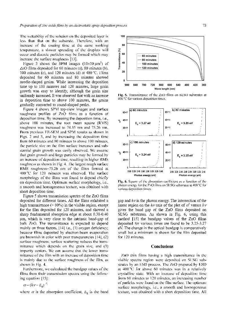
Figure 5 shows transmission spectra of the ZnO filmsdeposited for different times. All the films exhibited ahigh transmittance (> 80%) in the visible region, exceptfor the film deposited for 120 minutes, and showed asharp fundamental absorption edge at about 0.38-0.40μm, which is very close to the intrinsic band-gap ofbulk ZnO. The transmittance is expected to dependmainly on three factors, [14] i.e., (1) oxygen deficiency;because films deposited by electron-beam evaporationare brownish in color with poor transparencies [14], (2)surface roughness; surface scattering reduces the trans-mittance which depends on the grain size, and (3)impurity centers. We can assume that the lower trans-mittance of the film with an increase of deposition timeis mainly due to the surface roughness of the film, asshown in Fig. 4.
Furthermore, we calculated the bandgap values of thefilms from their transmission spectra using the follow-ing equation [15]:
α = (hν − Eg)1/2
where α is the absorption coefficient, Eg is the band
gap and hν is the photon energy. The intersection of thelinear region on the hν axis of the plot of α2 versus hνgives the band gap of the ZnO films deposited onSLSG substrates. As shown in Fig. 6, using thismethod [15] the bandgap values of the ZnO filmsdeposited for various times are found to be 3.25-3.27eV. The change in the optical bandgap is comparativelysmall but a minimum is shown for the film depositedfor 120 minutes.
Conclusions
ZnO thin films having a high transmittance in thevisible spectra region were deposited on SLSG sub-strates by an ESD process. The ZnO prepared by ESDat 400 oC for above 60 minutes was in a relativelycrystalline state. With an increase of deposition timefrom 60 minutes to 120 minutes, an increasing numberof particles were found on the film surface. The optimumsurface morphology, i.e., a smooth and homogeneoustexture, was obtained with a short deposition time. All
Fig. 5. Transmittance of the ZnO films on SLSG substrates at400 oC for various deposition times.
Fig. 6. Square of the absorption coefficient as a function of thephoton energy for the ZnO films on SLSG substrates at 400 oC forvarious deposition times.

74 Ju-Hyun Jeong, Young-Sun Jeon, Kyung-Ok Jeon, Kyu-Seog Hwang and Byung-Hoon Kim
the films exhibit a high transmittance (> 80%) in thevisible region, except for the film deposited for 120minutes, and show a sharp fundamental absorptionedge at about 0.38-0.40 μm.
References
1. Y. Chen, H. Ko, S. Hong, and T. Yao, Appl. Phys. Lett.76[5] (2000) 559-561.
2. Y. Chen, H. Ko, S. Hong, T. Yao, and Y. Segawq, J. Cryst.Growth 214/215 (2000) 87-91.
3. A.B.M. Ashrafi, B. Zhang, N. Ninh, K. Wakatsuki, and Y.Segawa, Jpn. J. Appl. Phys. 43 (2004) 1114-1117.
4. M. Chen, Z. Pei, X. Wang, C. Sun, and L. Wen, J. Mater.Res. 16[7] (2001) 2118-2123.
5. B. Zhao, H. Yang, G. Du, X. Fang, D. Liu, C. Gao, X. Liu,and B. Xie, Semicond. Sci. Tech. 19 (2004) 770-773.
6. Y. Chen, S. Hong, H. Ko, M. Nakajima, and T. Yao, Appl.
Phys. Lett. 76[2] (2000) 245-247.7. C. Lin, C. Hsiao, S. Chen, and S. Cheng, J. Electrochem.
Soc. 151[5] (2004) G285-G288.8. D. Mondelaers, G. Vanhoyland, H. Rul, J. D’haen, M.
Bael, J. Mullens, and L. Pouche, J. Sol-Gel Sci. & Tech. 26(2003) 523-526.
9. K. Choy, Mater. Sci. and Eng. C16 (2001) 139-145.10. R. Chandrasekhar, and K. Choy, Thin Solid Films 398-399
(2001) 59-64.11. C. Chen, K. Varhaug, and J. Schoonman, J. Mater. Syn.
and Proc. 4[3] (1996) 189-194.12. B. Kim, J. Jeong, Y. Jeon, K. Jeon, and K. Hwang,
submitted to J. Sol-Gel Sci. & Tech. (2005).13. N. Stelzer, and J. Schoonman, J. Mater. Syn. and Proc. 4[6]
(1996) 429-438.14. V. Gupta and A. Mansingh, J. Appl. Phys. 80[2] (1996)
1063-1073.15. K. Hwang, Y. Jeon, B. Kang, K. Nishio, T. Tsuchiya, J.
An, and B. Kim, J. Kor. Phys. Soc. 46[2] (2005) 521-526.