contentserives/382_10/fr_jansky.pdf · contents list of figures ... the second inverter circuit...
TRANSCRIPT

1
Contents List of Figures ................................................................................................................................................ 2
Chapter 1: Introduction ................................................................................................................................ 3
Chapter 2: Background ................................................................................................................................. 3
Chapter 3: Design .......................................................................................................................................... 3
3.1 Smart Battery Charger ........................................................................................................................ 3
3.1.1 Requirements ............................................................................................................................... 3
3.1.2 Design Alternatives and Selection ............................................................................................... 4
3.1.3 Components ................................................................................................................................. 4
3.2 DC/AC Power Supply ........................................................................................................................... 4
3.2.1 Requirements ............................................................................................................................... 4
3.2.2 Design Alternatives and Selection ............................................................................................... 5
3.2.3 Components ................................................................................................................................. 5
3.3 Measurement System ......................................................................................................................... 5
3.3.1 Requirements ............................................................................................................................... 5
3.3.2 Design Alternatives and Selection ............................................................................................... 6
3.3.3 Components ................................................................................................................................. 6
3.4 Monitor/Data Logger .......................................................................................................................... 6
3.4.1 Requirements ............................................................................................................................... 6
3.4.2 Design Alternatives and Selection ............................................................................................... 7
3.4.3 Components ................................................................................................................................. 7
3.5 Internet Interface ................................................................................................................................ 7
3.5.1 Requirements ............................................................................................................................... 7
3.5.2 Design Alternatives and Selection ............................................................................................... 7
3.5.3 Components ................................................................................................................................. 7
3.6 Overall System .................................................................................................................................... 8
3.6.1 Requirements ............................................................................................................................... 8
3.6.2 Design Alternatives and Selection ............................................................................................... 8
3.6.3 Components ................................................................................................................................. 8
Chapter 4: Implementation, Testing, and Analysis ....................................................................................... 8

2
4.1 Smart Battery Charger ........................................................................................................................ 9
4.2 DC/AC Power Supply ........................................................................................................................... 9
4.3 Measurement System ......................................................................................................................... 9
4.4 Monitor/Data Logger ........................................................................................................................ 11
4.5 Internet Interface .............................................................................................................................. 11
4.6 Overall System .................................................................................................................................. 11
Chapter 5: Conclusion ................................................................................................................................. 12
5.1 Future Works .................................................................................................................................... 12
5.2 Final Remarks .................................................................................................................................... 12
References .................................................................................................................................................. 12
Appendix A .................................................................................................................................................. 13
Appendix B .................................................................................................................................................. 16
Appendix C .................................................................................................................................................. 20
Appendix D .................................................................................................................................................. 21
Program Code for Measurement System ............................................................................................... 21
Code for Website .................................................................................................................................... 27
HTML Code .......................................................................................................................................... 27
Flash ActionScript Code ...................................................................................................................... 28
Appendix E .................................................................................................................................................. 30
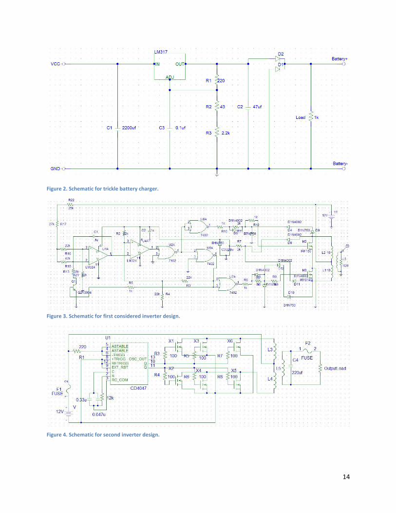
List of Figures Figure 1. Schematic for fast battery charger. ............................................................................................. 13
Figure 2. Schematic for trickle battery charger. ......................................................................................... 14
Figure 3. Schematic for first considered inverter design. ........................................................................... 14
Figure 4. Schematic for second inverter design. ......................................................................................... 14
Figure 5. Schematic for voltage and current measurment. ........................................................................ 15
Figure 6. Schematic for frequency and power factor measurement. ......................................................... 15
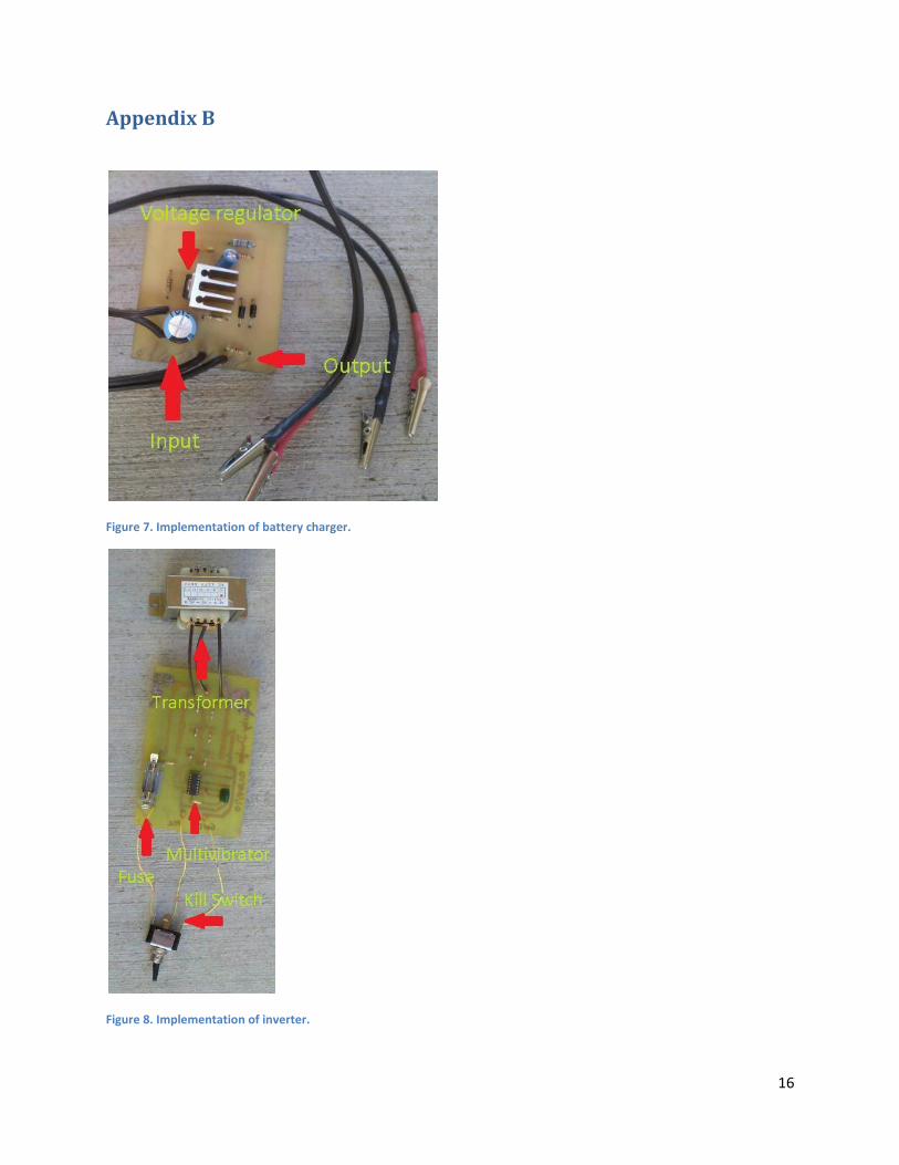
Figure 7. Implementation of battery charger. ............................................................................................ 16
Figure 8. Implementation of inverter. ........................................................................................................ 16
Figure 9. Implementation of measurement system. .................................................................................. 17
Figure 10. Screenshot of web interface. ..................................................................................................... 18
Figure 11. TS-7200 single board computer. ................................................................................................ 18
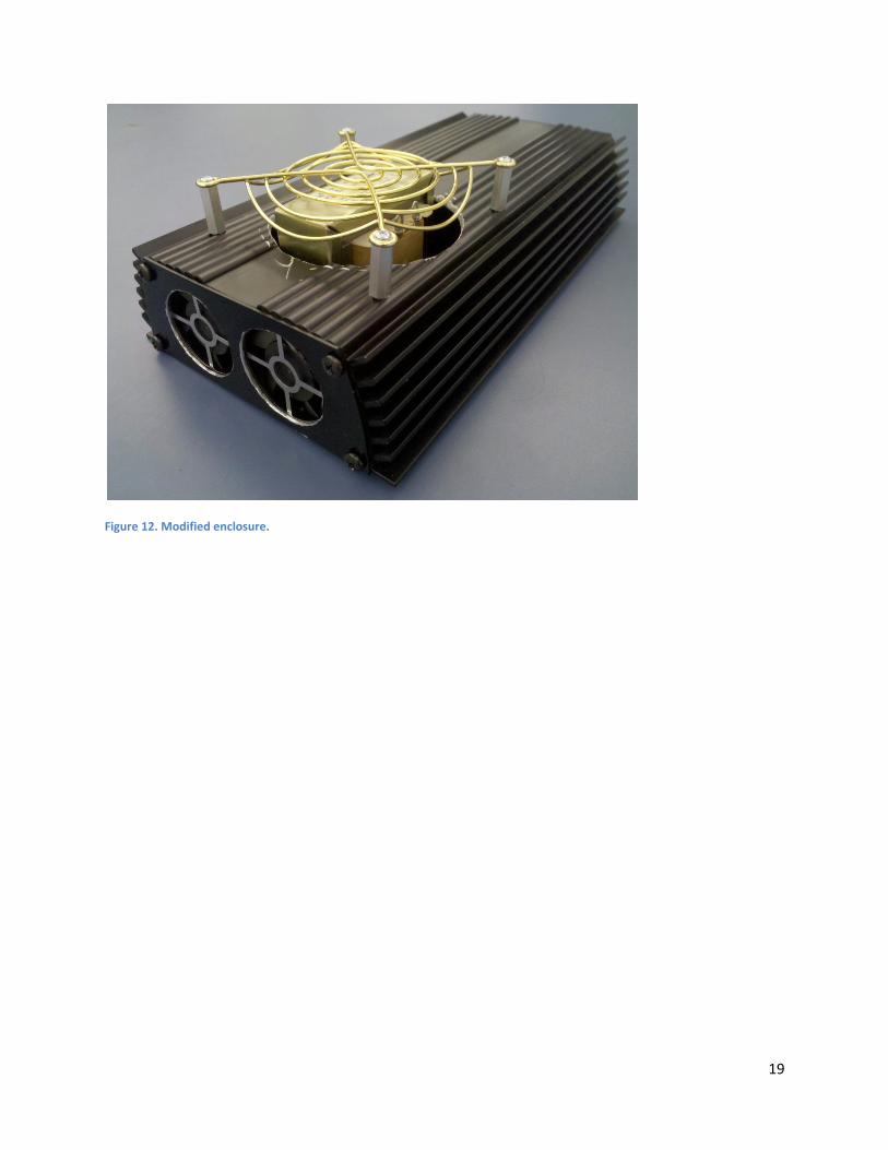
Figure 12. Modified enclosure. ................................................................................................................... 19
Figure 13. Flow chart of overall system. ..................................................................................................... 20

3
Figure 14. Current vs. Voltage plot for solar panels. .................................................................................. 20
Chapter 1: Introduction
Renewable energy has increased in popularity over the last couple of years due to advances in
technology. People have been running into problems when using renewable energy systems because of
the inconsistent power they deliver. The need for systems that harvest energy to batteries and then use
that stored energy, when conditions are less than ideal, are required for consistent power. A system like
the Intelligent DC-DC/AC converter can be used to provide consistent power to a load when sun and
wind conditions are not optimal.
Chapter 2: Background
Currently on the market there are three types of DC-AC converters: square wave, modified square wave,
and pure sine wave. The most inexpensive is the square wave converter, but is not used often due to its
poor power output. The modified square wave converter is also inexpensive, but also has a better power
output. The pure sine wave converter has the best power output but is the most expensive option.
Currently, commercially available converters do not have an internet monitoring capability. This
capability would allow for off-site monitoring and data backup. The most common type of converter is a
laptop car charger converter.
Chapter 3: Design
A flow chart of the overall system to be implemented can be seen in Appendix C- Figure 13. We have
obtained a current vs. voltage plot for the solar panels. This plot can be found in Appendix C- Figure 14.
3.1 Smart Battery Charger
3.1.1 Requirements
This subsystem is used to charge a bank of batteries and then float the voltage to zero when the
batteries have reached their maximum charge. Once the batteries have discharged passed a certain
point, the charger should resume charging the batteries. Since this subsystem provides produces a
reasonably high power output, safety mechanisms must be implemented to protect the device and its
users.

4
3.1.2 Design Alternatives and Selection
For this subsystem, we looked at two designs. The first charger system was a fast battery charger.1 We
considered this charger because of its high-performance capabilities. It is able to quickly charge a bank
of lead-acid batteries and turn off when the battery reaches a fully charged state. The battery charger
initially starts out with a current of 2 A. As the voltage rises to 12 V, the current decreases to 150 mA
and the charger automatically switches to a lower float voltage to keep from overcharging the bank of
batteries. This design also provided us with an LED to indicate the status of the battery. The schematic
for this design is in Appendix A- Figure 1.
Another option we looked at was a trickle battery charger. This circuit uses the LM317 voltage regulator
to regulate the voltage on the output terminals to charge a bank of lead-acid batteries. The design
creates a voltage difference of 13.1 V on the output which is used to charge the batteries. Once the
batteries are fully charged, the load resistor connected in parallel on the output terminals allows current
to flow through the load insuring that the battery is not overcharged and that it maintains a 13 V
potential. The current flowing into the battery depends on the status of the battery, but the design
limits the maximum current to around 2 A if the batteries’ potential is sufficiently low. The schematic for
this design is in Appendix A- Figure 2.
We chose the trickle charger for our design. The low cost of this design allowed us to allocate money to
other areas of our project, which required components that are more expensive. This design also
allowed us to rebuild, switch components, and change component values without a large increase in
cost. Fewer components for this design allowed us to implement this subsystem with a relatively
lightweight device. This lightweight device allowed us to quickly assemble the circuit for testing
purposes giving us more time to make needed modifications. The small footprint of the device was also
appealing to the design team because it allowed for more room for other subsystems in our compact
enclosure.
3.1.3 Components
The components needed to implement the trickle charger are:
2 Diodes
3 Capacitors
4 Resistors
1 LM317 Voltage Regulator
3.2 DC/AC Power Supply
3.2.1 Requirements
This subsystem should transform the online power of the solar panel and wind generator to 12 VDC and
120 VAC @ 60 Hz. Since this subsystem provides medium-high voltage, safety mechanisms should be
implemented to protect the device and users.

5
3.2.2 Design Alternatives and Selection
For this subsystem, we looked at inverter circuits that would provide the high power rating that this
subsystem is supposed to yield. The first inverter circuit considered was rated for a 500 W output with
the possibility of adding additional mosfet transistors to increase its output to 600 or 700 W. This circuit
uses NOR gates along with amplifiers to provide the switching necessary for the mosfets. The circuit was
designed to output a square wave of 120 V on the output terminals of the center-tapped transformer.
The schematic for this design is in Appendix A- Figure 3.
The second inverter circuit considered was rated at 500 W. This inverter uses the CD4047
monostable/astable multivibrator in combination with two capacitors and one resistor on pins 2-4 to
create alternating output voltages on Q and Q’. The output of Q and Q’ is used to switch mosfets, which
are constantly in saturation, whether the circuit is on or off. The switching of the mosfets allows current
to flow from the positive voltage terminal to ground through the center winding of the transformer. The
current flow through each winding causes a positive and negative voltage on the output to the
transformer, which is filtered to produce a 120 V sine wave. The schematic for this design is in Appendix
A- Figure 4.
Unfortunately upon construction of the first inverter circuit, we were unable to obtain the needed
output voltages to the mosfets to provide the 120 V output required. Thus, this early circuit was
abandoned for our second design, which involved fewer components. Instead of using the 2 amplifiers
and 4 NOR gates of the first design, the CD4047 that the second design uses was able to provide us with
the changing output voltages needed to switch our mosfets. This made our design more compact and
easier to build. The number of components needed to construct this inverter was much less then the
first design, which allowed for quick construction and debugging of our inverter. Fewer components in
this design also decreased our cost of construction. The lower cost allowed us to further reduce the
overall cost of the project and the opportunity to divert more money to other subsystems.
3.2.3 Components
The components needed to implement the inverter circuit are:
8 Resistors 3 Capacitors 1 IC CD4047 1 Transformer 12+12 V/240 V (500W) 6 Power mosfets
3.3 Measurement System
3.3.1 Requirements
This subsystem is used to measure the voltage, current, frequency, and power factor being provided to a
load. The sampling of these values should occur at twice the operating frequency so that real time
values can be recorded. Since this subsystem provides reasonably high voltage, safety mechanisms must
be implemented to protect the device and its users.

6
3.3.2 Design Alternatives and Selection
We had two hardware options for our measurement system. Our first design option was to use a
CS5461A integrated circuit (IC) from Cirrus. This was considered because it is from the same
manufacturer as the processor on the single board computer (SBC) we chose. This would reduce the risk
of complications interfacing the device with the TS-7200 IIC bus.
Our second design option was to design our system using discrete components. This option had the
benefits of knowing exactly how the power factor was being measured. It also gave us control of
designing for low power consumption, as well as allowing us to take advantage of the large processing
power of the TS-7200 to handle calculations.
We decided to go with designing our own system for three reasons. In researching this topic we found a
caution about ICs, warning that they do not always calculate power factor in the way introductory circuit
analysis teaches. This would result in research time to become familiar not only with interfacing with
the chip, but also with learning and understanding how it calculates the power factor and if this would
work in our system. The IC also requires some external circuit design to take the measurements it needs.
While this circuit is reduced in complexity from our own design, it would not likely save us enough time
to justify using the IC.
The design for the measurement system consisted of 4 circuits combined to acquire the required
measurements. The first two circuits worked to measure the voltage drop across a current sensing
resistor. The voltages were scaled down from 120 V to be between 0 and 3.3 volts which is the range of
the ADCs on the TS-7200. The third and fourth circuits were combined to measure the frequency and
power factor of the AC voltage being delivered to the load. One was placed before the load and one
after. The concept behind these circuits was to use comparator circuits to produce a square wave
corresponding to the positive half of the sinusoidal signal’s period. In testing, the results were accurate
compared to the supplied frequency with no measureable error. By measuring the time difference
between the comparator pulses we can calculate the power factor. The schematics for these circuits are
in Appendix A- Figures 5 and 6, respectively.
3.3.3 Components
The components needed to implement the measurement system are:
18 Resistors
4 Op-amps
3.4 Monitor/Data Logger
3.4.1 Requirements
This subsystem should record the data collected from the measurement system on a SD card or
computer. There are no safety requirements for this subsystem.

7
3.4.2 Design Alternatives and Selection
For this subsystem, we decided that a single board controller (SBC) would be the best option because of
the integrated system nature of these devices. We researched available devices and then narrowed the
decision down to two. One of the devices we found was the Modtronix SBC. This device had an Ethernet
port, 3936 Bytes of SRAM, analog-to-digital converters (ADCs), and pulse width modulators. The
software required to program this device was proprietary and the evaluation version would not yield
small file sizes for compilation. This was a major drawback considering the small amount of data space
available on the board.
The second device we found was the TS-7200. This device had a serial communication port, Ethernet
port, universal serial bus (USB), 32 mega bytes of SDRAM, ADCs, and a compact flash port. This device
also comes with a distribution of Linux on it. This allowed for programming in multiple languages and file
sizes. The compact flash card reader allowed for large data space which would be advantageous because
of the large amount of data the device will be recording.
We decided to go with the TS-7200 because of the increased number of communication options, larger
disk space for data, and ease of programming. This SBC was the most expensive of the options we
found, but we thought the price was justified by all the added features the device offered. This option
also allowed for customization by the end-user.
3.4.3 Components
Components used for this subsystem are the TS-7200 SBC.
3.5 Internet Interface
3.5.1 Requirements
This subsystem should upload the data collected and saved by the measurement system and
monitor/data logger to the Electrical Engineering (EE) web server and then display the data on a
website. There are no safety requirements for this subsystem.
3.5.2 Design Alternatives and Selection
It was required that the power factor, current, voltage, and frequency measurements made by the data
logger be displayed in real time on the EE web server. To create this subsystem, several methods were
considered. One option was to use HTML (HyperText Markup Language) to hard code a web page that
would display the required information, but this option was unfamiliar and would thus require too much
time in research and troubleshooting. Another option was MySQL, a relational database management
system, but, similar to HTML, this option was even more unfamiliar. The method chosen to create this
subsystem was that of Adobe Flash. This option was chosen because of the knowledge of the language,
ease of use, and ability to create high quality websites.
3.5.3 Components
The components needed to implement this subsystem are:
EE Web Server

8
Adobe Flash CS3
Adobe Dreamweaver CS3
3.6 Overall System
3.6.1 Requirements
All the subsystems should be contained in an enclosure to provide protection for the components and
for the users of the device. Safety mechanisms and cooling systems should also be implemented for
protection.
3.6.2 Design Alternatives and Selection
To accomplish the safety and enclosure requirements, we looked into many different options that could
be implemented in our designs. We found that for current restrictions, fuses or current limiters could be
used. For voltage restrictions, circuit breakers or voltage regulators could be used. For heat precautions,
fans or heat sinks could be used. For the enclosure, many options were available but few fit our needs.
We also looked at how we could interface with a load for AC and DC output. We researched using a
standard wall outlet or an extension cord female connector for AC power. For DC power, we looked at
using a DC plug port.
We chose to implement fuses for current restrictions because of their lower cost and operating
requirements. We chose to implement voltage regulators for voltage restrictions because most of our
designs already utilized this option. For heating precautions, we decided it would be best to use both
heat sinks and fans to deal with heat. This decision was made based off the fact that some of the circuits
are high-powered and produce a lot of heat. For the enclosure, we found an aluminum enclosure that
doubles as a heat sink. This option was the best we found because it was inexpensive and helped with
heat dissipation. We found that for connections to AC power, mounting an extension cord female
connector would be the most practical solution and convenient for the user. For DC power, the DC plug
port was the best option we found.
3.6.3 Components
The components needed to implement these safety precautions are:
Fuses
Voltage regulators
Heat sinks
Fans
Aluminum Enclosure
Extension cord female connector
DC plug port
Chapter 4: Implementation, Testing, and Analysis

9
4.1 Smart Battery Charger This subsystem has been designed and a circuit board has been made using the design choice previously
mentioned. We have tested the subsystem on a 12 V battery and have found that it properly charges
and maintains the battery at full capacity. This system is fully functional and finished. A picture of the
implemented circuit can be seen in Appendix B- Figure 7.
4.2 DC/AC Power Supply The chosen design for this subsystem has been tested on a breadboard in the analog lab. It was
measured and found to have a square wave output with 124 Vrms and 62 Hz. Since testing was
successful, an etched circuit board has been made. We still need to implement the filter to make the
square wave into a sine wave. This system has not been tested with the wind generator or solar panels.
A picture of the etched circuit can be seen in Appendix B- Figure 8.
4.3 Measurement System The design for the measurement system consisted of 4 circuits combined to take the required
measurements. The first two circuits worked to measure the voltage drop across a current sense
resistor. The voltages were scaled down from 120 V to be between 0 and 3.3 V which is the range of the
ADCs of the TS-7200.
The first issue overcome was that of keeping the sinusoidal voltage in the 0 to 3.3 V range with no DC
offset so that if contain both positive and negative values. One solution we considered was to use
diodes to rectify the signal. The advantage of this method is its simplicity. It however is not a possible
choice in itself because of the –0.7 V drop before it clips the negative signal. At an absolute maximum
the ADC could handle a -.2 V signal. We next considered Schottky diodes due to their reduced voltage
drop, however we were unable to locate any with such a small drop. Next we considered super diodes
which are able to reduce the voltage drop to around 0 V because of the use of the feedback path around
the op-amp. The super diodes we tried proved to be unstable when using a single sided supply. Using
more expensive op-amps for this approach might have had more reasonable results.
We finally settled on a voltage divider to scale down the voltage source, while using a non-inverting
summer to provide the needed DC offset. When the circuit was tested alone it functioned as expected
providing a scaled down sinusoid with the correct DC offset.
The third and fourth circuits were combined to measure the frequency and power factor of the voltage
being delivered to the load. One was placed before the load and one after. The design behind these
circuits was to use comparator circuits to produce a square wave corresponding to the positive half of
the sinusoidal signal’s period. In testing the results were accurate according to the supplied frequency
with no measureable error. By measuring the difference in time between the comparator pulses we
were able to calculate the power factor.
The issue we next encountered was that of implementing all of these circuits together. In testing these
circuits in the lab we found issues with supplying the op amps with available single sided supplies as
none of them were true single supply op-amps. We resolved this by providing a virtual ground of one

10
half the supply voltage. We have been unable to successfully integrate all 4 circuits together. The issue
that we are facing is that the signal generators are trying to provide 12 V in the test lab. However, when
connected to our circuits they only supply a fraction of that, as low as ½ a volt. We believe this is due to
some part of the circuit drawing large currents and therefore loading down the test equipment so that it
cannot provide the voltage it is designed too. We have not yet been able to locate what portion of the
circuit is causing this issue. A picture of the circuits wired on a breadboard can be seen in Appendix B-
Figure 9.
The software side of the measurement system is a C program loaded to the SBC that is designed to read
in the values and perform the needed calculations to provide accurate output for monitoring. The
voltage and current measurement code reads in the scaled down value of the voltage across the current
sense resistor. Using the ratios of the dividers it calculates the peak values being supplied. From these it
calculates the root mean square values being supplied.
The frequency is measured by recording the time between rising edges of the pulse generated by the
first comparator circuit. This is the time of one period of the signal. Using this we calculate the
frequency which is the inverse of the measured period. In order to calculate the power factor we
measure the time difference between the two comparator’s rising edge pulses. By comparing which
edge occurred first and the time between them we obtain accurate results. We use a timing function in
our code that takes advantage of Linux times functions timing in C. This function allows us to have up to
micro-second accuracy.
The only significant issue with writing the program for this section is that we initially intended to use
interrupts to time the rising edges to have our highest level of accuracy. Due to our inexperience with
programming these tasks with a Linux based operating system we were unaware that an operating
system between our program and the hardware we were unable to directly access interrupts and would
need to make use of the Linux kernel to use them. We overcame this by using the large processing
power at our disposal with the TS-7200. With a 200MHz clock speed it takes only 5 nano-seconds per
clock cycle. Accessing our timing function takes only 3 clock cycles. It takes far more time than any other
functions combined to measure the power factor, which is the only place where this would be an issue.
This allowed us to ignore the use of interrupts and instead use the technique of polling, or constantly
monitoring the status registers for changes that indicate the rising edge of a pulse without a measurable
loss in accuracy.
We had an issue of a delayed parts order which set back our progress by a week and delayed our ability
to build and test the circuit hardware. Had this been avoided we might have been able to isolate the
source of excessive current in the physical hardware. The software has yet to be tested as we have had
several issues with updating and configuring the operating system to a point where it was operable from
which we could test it. As of the writing of this paper we have just today been able to have the board
ready enough for the programmer to transfer and test the code to the board. Had the board come
preconfigured this issue might have also been avoided. The code for the program written is included in
Appendix D.

11
4.4 Monitor/Data Logger We are having issues implementing the internet communication between the TS-7200 and the EE server.
We have talked to many different sources about how to resolve the problem. One solution is that the
TS-7200 be connected to a port that does not have any network blocking (outside the EE department).
We have tried to connect the board to an Ethernet port in the on-campus apartments. This did not fix
the problem. Another possible solution to find examples of how to edit the configuration files on the TS-
7200. We have tried many different combinations of configuration techniques, but none have been
successful. We had been having power issues in which the board would keep resetting while booting up.
The manufacturer has been contacted and said that this issue had been reported, but that they
currently have no solution. The resetting issue has gone away, but the networking issue may be fallout
from the initial resetting issue. Picture of TS-7200 SBC has been included in Appendix B- Figure 11.
4.5 Internet Interface The method chosen to create this subsystem was that of Adobe Flash. Being familiar with this program
and already having an idea of how to accomplish the task, Flash ActionScript 3.0 code was written to
extract the data from each measurement uploaded to the server by the SBC. Once extracted, the
program displays the power factor, current, voltage, frequency, and battery level values on the screen in
an attractive and easily readable manner. The Flash program was then set to loop so that it would
continue reading in each new measurement file the SBC uploaded to the server. HTML code was then
written using Adobe Dreamweaver to contain the Flash file and display it in a web page. The code for
the website can be seen in Appendix D.
The Flash and HTML files were then uploaded to the EE web server at geek.nmt.edu/~jansky and tested.
The page was loaded with a Firefox web browser where it was found to display the files correctly.
PuTTY, an SSH (Secure Shell network protocol) client was used to save text files containing measurement
values to the server. The Flash program was then tested and found to successfully read in each
measurement and display them accordingly. The SSH protocol was repeated several times, sending new
text files with new measurement values of which the Flash program displayed in real time. A screenshot
of the website can be seen in Appendix B- Figure 10.
4.6 Overall System We have prepared our enclosure for mounting the components. We have cut holes for the fans, vents,
and ports of the SBC. We have mounted the transformer in such a way so that it does not over heat or
present a potential shock hazard. Since we are still trying to finish unfinished subsystems, we have not
put all units in the enclosure. A picture of the enclosure can be seen in Appendix B- Figure 12.

12
Chapter 5: Conclusion
5.1 Future Works As mentioned above, not all of our systems have been fully completed and tested. We are currently
undergoing testing of the battery charger and inverter with the wind generator and solar panels. We are
trying to document what their output is with the generators powering them. We are still trying to figure
out what needs to be done to get the TS-7200 communicating with the EE server. As for the
measurement system, we have been advised by Dr. Erives to try to get the voltage and current
measurement system working. Integration of the two systems has proven difficult and due to the
limited time we have, this seems to be the best way to proceed. We have included a budget and
semester timeline in Appendix E.
5.2 Final Remarks At the time of writing this paper, we have not completed all of the requirements of this project. We
have had some setbacks due to circuit redesigns, ordering issues, and possibly defective parts. We have
worked as hard as we could to deal with the issues we have encountered but due to the limited time we
had to complete this project we have not dealt with all of them. Part of Junior Design is preparing
students for industry. We have learned firsthand that sometimes you don’t fully succeed at a task you
have been given. We have learned a lot over the course of this semester and feel more confident that
we will be able to use what we have learned for Senior design and for our careers as engineers.
References 1-Encyclopedia of Electronic Circuits Volume 1 by Rudolf F. Graf. p 111.
General information about circuit design obtained from the following sources:
Microelectronic Circuits 5th edition (Oxford, 2004), Sedra and Smith
The Art of Electronics. Horowitz and Hill

13
Appendix A
Figure 1. Schematic for fast battery charger.
14
Figure 2. Schematic for trickle battery charger.
Figure 3. Schematic for first considered inverter design.
Figure 4. Schematic for second inverter design.
15
Figure 5. Schematic for voltage and current measurment.
Figure 6. Schematic for frequency and power factor measurement.
16
Appendix B
Figure 7. Implementation of battery charger.
Figure 8. Implementation of inverter.

17
Figure 9. Implementation of measurement system.

18
Figure 10. Screenshot of web interface.
Figure 11. TS-7200 single board computer.
19
Figure 12. Modified enclosure.

20
Appendix C
Figure 13. Flow chart of overall system.
Figure 14. Current vs. Voltage plot for solar panels.

21
Appendix D
Program Code for Measurement System #include <unistd.h>
#include <sys/types.h>
#include <sys/mman.h>
#include <stdio.h>
#include <stdlib.h>
#include <fcntl.h>
#include <assert.h>
#include<string.h>
#include <iostream>
#include <ctime>
#include <sys/time.h>
#include <math.h>
#include "peekpoke.h"
#include "eeprog.h"
#include "ep93xx_adc.h"
#define DATA_PAGE 0x80840000
#define CALIB_LOC 2027 //location of calibration values
/* Prototypes */
static void read_7xxx_adc(int adc_result[5][10]);
void print_ADC_channels();
/* globals */
static unsigned long dr_page, adc_page, syscon_page, pld_page;
int main(void)
{
int devmem = open("/dev/mem", O_RDWR|O_SYNC);
assert(devmem != -1);
FILE *fp;
fp=fopen("/dev/mem/test.txt", "r");
dr_page = (unsigned long)mmap(0, getpagesize(), PROT_READ|PROT_WRITE
, MAP_SHARED, devmem, DATA_PAGE);
assert(&dr_page != MAP_FAILED);
spistart = (unsigned long)mmap(0, getpagesize(),
PROT_READ|PROT_WRITE,
MAP_SHARED, devmem, SPI_PAGE);
assert(&spistart != MAP_FAILED);
adc_page = (unsigned long)mmap(0, getpagesize(),
PROT_READ|PROT_WRITE,
MAP_SHARED, devmem, ADC_PAGE);
assert(&adc_page != MAP_FAILED);
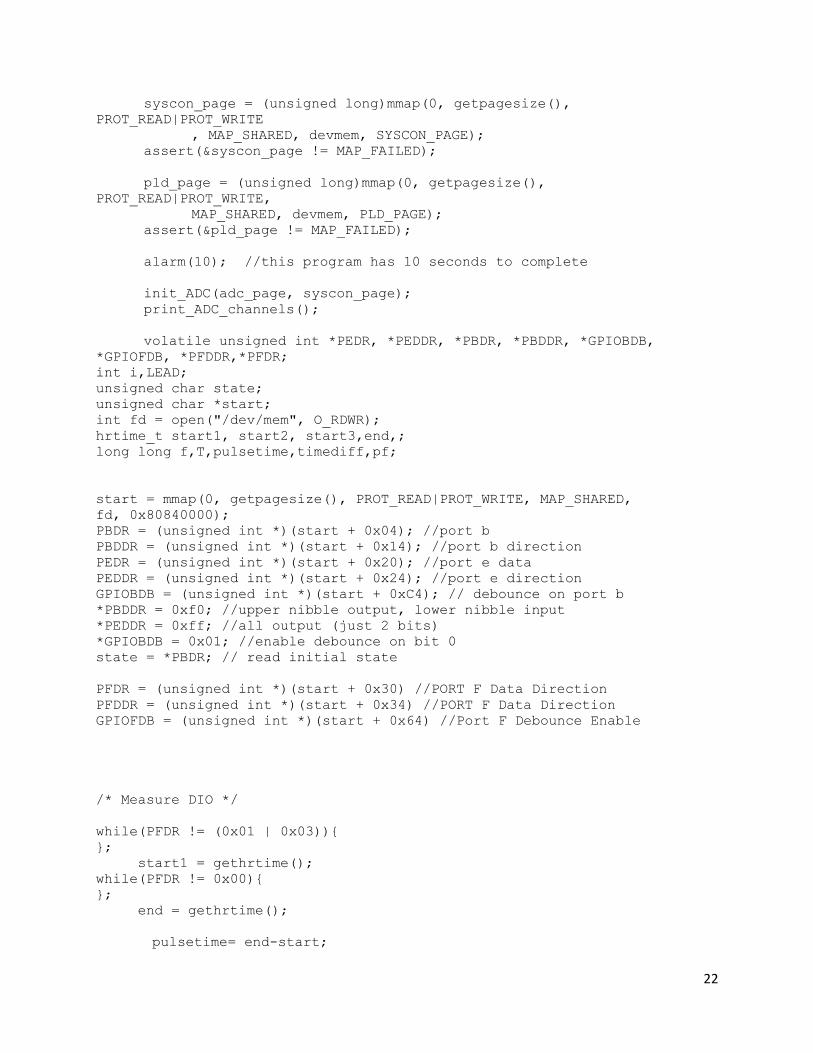
22
syscon_page = (unsigned long)mmap(0, getpagesize(),
PROT_READ|PROT_WRITE
, MAP_SHARED, devmem, SYSCON_PAGE);
assert(&syscon_page != MAP_FAILED);
pld_page = (unsigned long)mmap(0, getpagesize(),
PROT_READ|PROT_WRITE,
MAP_SHARED, devmem, PLD_PAGE);
assert(&pld_page != MAP_FAILED);
alarm(10); //this program has 10 seconds to complete
init_ADC(adc_page, syscon_page);
print_ADC_channels();
volatile unsigned int *PEDR, *PEDDR, *PBDR, *PBDDR, *GPIOBDB,
*GPIOFDB, *PFDDR,*PFDR;
int i,LEAD;
unsigned char state;
unsigned char *start;
int fd = open("/dev/mem", O_RDWR);
hrtime_t start1, start2, start3,end,;
long long f,T,pulsetime,timediff,pf;
start = mmap(0, getpagesize(), PROT_READ|PROT_WRITE, MAP_SHARED,
fd, 0x80840000);
PBDR = (unsigned int *)(start + 0x04); //port b
PBDDR = (unsigned int *)(start + 0x14); //port b direction
PEDR = (unsigned int *)(start + 0x20); //port e data
PEDDR = (unsigned int *)(start + 0x24); //port e direction
GPIOBDB = (unsigned int *)(start + 0xC4); // debounce on port b
*PBDDR = 0xf0; //upper nibble output, lower nibble input
*PEDDR = 0xff; //all output (just 2 bits)
*GPIOBDB = 0x01; //enable debounce on bit 0
state = *PBDR; // read initial state
PFDR = (unsigned int *)(start + 0x30) //PORT F Data Direction
PFDDR = (unsigned int *)(start + 0x34) //PORT F Data Direction
GPIOFDB = (unsigned int *)(start + 0x64) //Port F Debounce Enable
/* Measure DIO */
while(PFDR != (0x01 | 0x03)){
};
start1 = gethrtime();
while(PFDR != 0x00){
};
end = gethrtime();
pulsetime= end-start;

23
f=1/(2*pulsetime);
T=2*pulsetime;
while(PFDR !=(0x01 |0x03)){
};
start1=gethrtime();
while(PFDR !=(0x02 | 0x03)){
};
start2=gethrtime();
pulsetime=start2-start1;
if ((timediff>pulsetime)&(timediff<2*pulsetime)){
LEAD=1;
timediff=2*pulse-start2;
pf=2*f*timediff*180;
};
else if((timediff>2*pulsetime)&(timediff<5/2)){
LEAD=0;
timediff=start2-2*pulse;
pf=2*f*timediff*180;
};
double fputc( double accurrent, File *fp);
double fputc( double vac, File *fp);
double fputc( double pf, File *fp);
double fputc( double f, File *fp);
fclose(fp);
close(devmem);
return 0;
}
/************************************************************************
*DESCRIPTION: Read all five of the EP93xx onboard ADC. Discard the first
*two samples then save the next 10.
***********************************************************************/
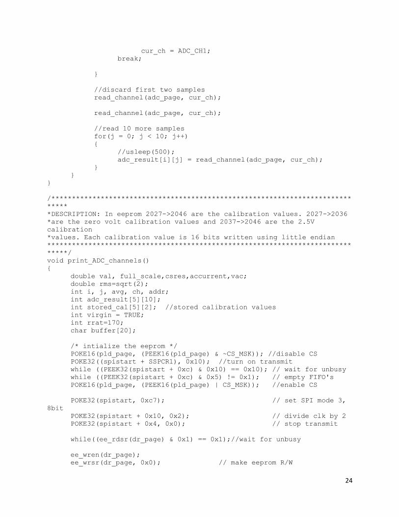
static void read_7xxx_adc(int adc_result[5][10])
{
int i, j, cur_ch;
for(i = 0; i < 2; i++)
{
switch(i)
{
case 0:
cur_ch = ADC_CH0;
break;
case 1:
24
cur_ch = ADC_CH1;
break;
}
//discard first two samples
read_channel(adc_page, cur_ch);
read_channel(adc_page, cur_ch);
//read 10 more samples
for(j = 0; j < 10; j++)
{
//usleep(500);
adc_result[i][j] = read_channel(adc_page, cur_ch);
}
}
}
/*************************************************************************
*****
*DESCRIPTION: In eeprom 2027->2046 are the calibration values. 2027->2036
*are the zero volt calibration values and 2037->2046 are the 2.5V
calibration
*values. Each calibration value is 16 bits written using little endian
**************************************************************************
*****/
void print_ADC_channels()
{
double val, full_scale,csres,accurrent,vac;
double rms=sqrt(2);
int i, j, avg, ch, addr;
int adc_result[5][10];
int stored_cal[5][2]; //stored calibration values
int virgin = TRUE;
int rrat=170;
char buffer[20];
/* intialize the eeprom */
POKE16(pld_page, (PEEK16(pld_page) & ~CS_MSK)); //disable CS
POKE32((spistart + SSPCR1), 0x10); //turn on transmit
while ((PEEK32(spistart + 0xc) & 0x10) == 0x10); // wait for unbusy
while ((PEEK32(spistart + 0xc) & 0x5) != 0x1); // empty FIFO's
POKE16(pld_page, (PEEK16(pld_page) | CS_MSK)); //enable CS
POKE32(spistart, 0xc7); // set SPI mode 3,
8bit
POKE32(spistart + 0x10, 0x2); // divide clk by 2
POKE32(spistart + 0x4, 0x0); // stop transmit
while((ee_rdsr(dr_page) & 0x1) == 0x1);//wait for unbusy
ee_wren(dr_page);
ee_wrsr(dr_page, 0x0); // make eeprom R/W

25
while((ee_rdsr(dr_page) & 0x1) == 0x1);//wait for unbusy
/* Read in the calibration values */
addr = CALIB_LOC;
for(i = 0; i < 20; i++)
{
ee_read_byte(dr_page, addr, &buffer[i]);
//check if board has stored calibration values
if(buffer[i] != 0xFF)
virgin = FALSE;
addr++;
}
//convert to 16 bit values
j = 0;
ch = 0;
for(i = 0; i < 20; i = i + 2)
{
if(i == 10)
{
ch = 0;
j = 1;
}
stored_cal[ch][j] = (buffer[i] | (buffer[i+1] << 8));
ch++;
}
//Read the adc values for all 2 channels
read_7xxx_adc(adc_result);
//Convert to voltage
for(i = 0; i < 2; i++)
{
avg = 0;
full_scale = (((((double)(stored_cal[i][1] + 0x10000)
- stored_cal[i][0]) / 2.5 ) * 3.3 ));
for(j = 0; j < 10; j++)
avg = adc_result[i][j] + avg;
avg = avg / 10;
if(avg < 0x7000)
avg = avg + 0x10000;

26
if(virgin == TRUE) //use approximation
{
avg = avg - 0x9E58;
val = ((double)avg * 3.3) / 0xC350;
}
else //use calibration values
{
avg = avg - stored_cal[i][0];
val = ((double)avg * 3.3) / full_scale;
}
/*calculate current using ohms law v=i*r*/
if(i=0){
vac1=val;
}
if(i=1){
vac2=val;
}
}
/*rrat is the ratio of the voltage divider rearranged to find the
value being delivered to the load, since this is a constant value
there is no need to wast cpu cycles to calculate it */
vac=(vac2*rrat)/rms; //voltage supplied to load
accurrent=(((v1-v2)/csres)*rrat)/rms; //current supplied to load
//make eeprom RO
ee_wren(dr_page);
ee_wrsr(dr_page, 0x1c);
}

27
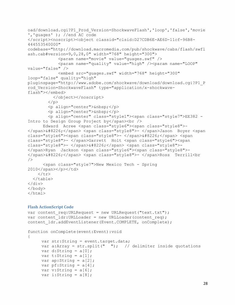
Code for Website
HTML Code <!DOCTYPE html PUBLIC "-//W3C//DTD XHTML 1.0 Transitional//EN"
"http://www.w3.org/TR/xhtml1/DTD/xhtml1-transitional.dtd">
<html xmlns="http://www.w3.org/1999/xhtml">
<head>
<meta http-equiv="Content-Type" content="text/html; charset=utf-8" />
<title>Jansky Design - System Monitor</title>
<style type="text/css">
<!--
body,td,th {
color: #FFFFFF;
}
body {
background-color: #000000;
background-image: url(bg.jpg);
background-repeat: no-repeat;
}
.style1 {
color: #888888;
font-family: Arial, Helvetica, sans-serif;
font-size: small;
}
.style6 {color: #7896FF}
.style7 {color: #555555}
.style8 {color: #000000}
-->
</style>
<script src="Scripts/AC_RunActiveContent.js"
type="text/javascript"></script>
</head>
<body>
<div align="center">
<table width="660" border="0" cellspacing="0" cellpadding="0">
<tr>
<td><p align="left"> </p>
<p align="left"> </p>
<p align="left"> </p>
<p align="left"> </p>
<p align="left"><br />
</p>
<p align="center">
<script type="text/javascript">
AC_FL_RunContent(
'codebase','http://download.macromedia.com/pub/shockwave/cabs/flash/sw
flash.cab#version=9,0,28,0','width','768','height','300','src','guages
','quality','high','pluginspage','http://www.adobe.com/shockwave/downl
28
oad/download.cgi?P1_Prod_Version=ShockwaveFlash','loop','false','movie
','guages' ); //end AC code
</script><noscript><object classid="clsid:D27CDB6E-AE6D-11cf-96B8-
444553540000"
codebase="http://download.macromedia.com/pub/shockwave/cabs/flash/swfl
ash.cab#version=9,0,28,0" width="768" height="300">
<param name="movie" value="guages.swf" />
<param name="quality" value="high" /><param name="LOOP"
value="false" />
<embed src="guages.swf" width="768" height="300"
loop="false" quality="high"
pluginspage="http://www.adobe.com/shockwave/download/download.cgi?P1_P
rod_Version=ShockwaveFlash" type="application/x-shockwave-
flash"></embed>
</object></noscript>
</p>
<p align="center"> </p>
<p align="center"> </p>
<p align="center" class="style1"><span class="style7">EE382 -
Intro to Design Group Project by</span><br />
Edward Acree <span class="style6"><span class="style8">-
</span>•</span> <span class="style8">- </span>Jason Boyer <span
class="style6"><span class="style8">- </span>•</span> <span
class="style8">- </span>Garrett Holt <span class="style6"><span
class="style8">- </span>•</span> <span class="style8">-
</span>Ryan Jackson <span class="style6"><span class="style8">-
</span>•</span> <span class="style8">- </span>Ross Terrill<br
/>
<span class="style7">New Mexico Tech - Spring
2010</span></p></td>
</tr>
</table>
</div>
</body>
</html>
Flash ActionScript Code var content_req:URLRequest = new URLRequest("text.txt");
var content_ldr:URLLoader = new URLLoader(content_req);
content_ldr.addEventListener(Event.COMPLETE, onComplete);
function onComplete(event:Event):void
{
var str:String = event.target.data;
var a:Array = str.split(" "); // delimiter inside quotations
var d:String = a[0];
var t:String = a[1];
var ap:String = a[2];
var pf:String = a[4];
var v:String = a[6];
var i:String = a[8];

29
var f:String = a[10];
var b:String = a[12];
var pf_n:Number = a[4];
var v_n:Number = a[6];
var i_n:Number = a[8];
var f_n:Number = a[10];
var b_n:Number = a[12];
date.text = d+" at "+t+" "+ap;
// ***** rotation = *_n/increment*20degrees *****
pf_txt.text = pf;
pf_needle.rotation = 20+pf_n/12.5*20; // rotates from 0-100
v_txt.text = v;
v_needle.rotation = v_n*20; // rotates from 0-14
i_txt.text = i;
i_needle.rotation = i_n/2*20; // rotates from 0-28
f_txt.text = f;
f_needle.rotation = f_n/10*20; // rotates from 0-80
b_txt.text = b;
b_bar.width = b_n*0.6; // total width (59.7) at b_n = 100
}

30
Appendix E
Budget
Amount Given $400.00
Battery Charger
Components Quantity Ordered
Total
Components Used
Cost of Used Component
Total Cost of Components ordered
Capacitors 3 3 $3.90 $3.90
Diodes 2 2 $0.04 $0.04
Resistors 4 4 $1.20 $1.20
LM317 1 1 $0.80 $0.80
PCB 1 1 $4.00 $4.00
Total Cost $9.94 $9.94
Inverter
Components
Quantity
Ordered
Total
Components
Used
Cost of Used
Component
Total Cost of
Components ordered
Capacitors 3 3 $3.90 $3.90
CD4047 2 1 $0.52 $1.04
Power Transistors 12 0 $0.00 $21.00
Resisoters 8 8 $2.40 $2.40
Transformer 1 1 $30.00 $30.00
Power Mosfets 6 6 $16.80 $16.80
16 AWG 1 1 $11.80 $16.95
PCB 1 1 $4.00 $4.00
Total Cost $69.42 $96.09
TS-7200
Components Quantity Ordered
Total
Components Used
Cost of Used Component
Total Cost of Components ordered
TS-7200 Board 1 1 $160.00 $160.00
TS-7200 Cable 1 1 $9.00 $9.00
Total Cost $169.00 $169.00

31
Other Costs
Components Quantity Ordered
Total
Components Used
Cost of Used Component
Total Cost of Components ordered
Compacted Flash
Card/wireless 1 1 $24.00 $24.00
TS-7200 Power
Supply 1 1 $32.00 $32.00
Other Components 1 1 $20.00 $20.00
Total Cost $76.00 $76.00
Total Cost Of Project
Components Quantity Ordered
Total
Components Used
Cost of Used Component
Total Cost of Components ordered
Battery Charger 1 1 $9.94 $9.94
Inverter 1 1 $69.42 $96.09
TS-7200 1 1 $169.00 $169.00
Other Costs 1 1 $76.00 $76.00
Total Cost $324.36 $351.03
Current Funds Used Cost Unused Cost
Amount Given $400.00 $400.00
Total Cost Of Project $324.36 $351.03
Difference $75.64 $48.97

32