inverter,design inverter
TRANSCRIPT
8/13/2019 Inverter,design inverter
http://slidepdf.com/reader/full/inverterdesign-inverter 1/51
ANALYSIS OF TWO LEVEL AND
THREE LEVEL INVERTERS
A PROJECT REPORT SUBMITTED IN PARTIALFULFILLMENT OF THE REQUIREMENTS FOR THE DEGREE
OF BACHELOR OF TECHNOLOGY IN “ELECTRICAL
ENGINEERING”
BY
PIYUS MOHANTY(10602010)
SARANSH SAHOO(10602058)
DEPARTMENT OF ELECTRICAL ENGINEERING NATIONAL INSTITUTE OF TECHNOLOGY, ROURKELA
ROURKELA-769008
8/13/2019 Inverter,design inverter
http://slidepdf.com/reader/full/inverterdesign-inverter 2/51
Department of Electrical Engineering
National Institute of Technology, Rourkela
Rourkela-769008, Orissa
CERTIFICATEThis is to certify that the work in the project report entitled “Analysis of two level and three level
inverters” by Piyus Mohanty(10602010) and Saransh Sahoo(10602058) has been carried out
under my supervision in partial fulfillment of the requirement for the degree of Bachelor of
Technology in “Electrical Engineering” during session 2008-09 in the Department of
Electrical Engineering, National Institute of Technology, Rourkela and this work has not
been submitted elsewhere for a degree.
PROF. A.K.PANDA
Place: N.I.T ROURKELA Professor, Department of
Date:10.5.2010 Electrical Engineering
National Institute of Technology,
Rourkela

8/13/2019 Inverter,design inverter
http://slidepdf.com/reader/full/inverterdesign-inverter 3/51
ACKNOWLEDGEMENTS
With a deep sense of gratitude, I wish to express my sincere thanks to my guide, Prof. A.K.
Panda, Professor, Electrical Engineering Department for giving us the opportunity to work
under him on this thesis. I truly appreciate and value his esteemed guidance and encouragement
from the beginning to the end of this thesis. We are extremely grateful to him. His knowledge
and company at the time of crisis would be remembered lifelong. We want to thank all my
teachers Prof. B.D.Subudhi, Prof. S.Rauta,Prof P.C.Panda,Prof. K.B. Mohanty, Prof.
D.Patra, Prof. S.Das, Prof. P.K. Sahu for providing a solid background for my studies and
research thereafter. They have been great sources of inspiration to us and we thank them from
the bottom of my heart. We will be failing in our duty if we do not mention the laboratory staff
and administrative staff of this department for their timely help. We also want to thank our
parents, who taught us the value of hard work by their own example. We would like to share this
moment of happiness with our parents. They rendered us enormous support during the whole
tenure of our stay in NIT Rourkela. Finally, we would like to thank all whose direct and indirect
support helped us completing our thesis in time. We would like to thank our department for giving us
the opportunity and platform to make our effort a successful one.
PIYUS MOHANTY
(10602010)
SARANSH SAHOO
(10602058)
8/13/2019 Inverter,design inverter
http://slidepdf.com/reader/full/inverterdesign-inverter 4/51
CONTENTSChapter No. Description Page No
CHAPTER 1 Introduction………………………………………………………….. 1
1.1 PROJECT OUTLINE
1.2 INVERTER
CHAPTER 2 Pulse Modulation Schemes………………………………………….. 3
2.1 PULSE AMPLITUDE MODULATION
2.2 PULSE WIDTH MODULATION
2.3 PULSE POSITION MODULATION
2.4 PULSE CODE MODULATION
2.5 ADVANTAGES OF PWM
CHAPTER 3 Pulse Width Modulation…………………………………………… 5
3.1 LINEAR MODULATION
3.2 SAW TOOTH PWM
3.3 REGULAR SPACED PWM
CHAPTER 4 Single Phase PWM Inverters………………………………………. 8
4.1 SINGLE PULSE WIDTH MODULATION
4.2 MULTIPLE PULSE WIDTH MODULATION
4.3 SINUSOIDAL PULSE WIDTH MODULATION
CHAPTER 5 PWM strategies with differing phase relationships……………….. 10
8/13/2019 Inverter,design inverter
http://slidepdf.com/reader/full/inverterdesign-inverter 5/51
5.1 ALTERNATE PHASE OPPOSITION DISPOSITION
5.2 PHASE OPPOSITION DISPOSITION
5.3 PHASE DISPOSITION
CHAPTER 6 Applications in harmonic elimination……………………………….. 19
6.1 NON LINEAR LOADS
6.2 ACTIVE POWER FILTERS
6.3 SHUNT ACTIVE POWER FILTERS
6.4 MODELLING OF THREE WIRE SHUNT ACTIVE
FILTERS
6.5 SYSTEM DESCRIPTION
6.6 MAINS SUPPLY
6.7 NON LINEAR LOAD
6.8 ROLE OF INVERTERS IN ACTIVE FILTERS
6.9 INTERFACE REACTOR
6.10 REFERENCE CURRENT GENERATION
6.11 CURRENT CONTROLLER
6.12 SIMULATION RESULTS
CHAPTER 7 Multi level inverters……………………………………………… 35
7.1 INTRODUCTION
7.2 DIFFERENT STRUCTURES OF MULTILEVEL
INVERTERS

8/13/2019 Inverter,design inverter
http://slidepdf.com/reader/full/inverterdesign-inverter 6/51
7.3 MULTILEVEL INVERTERS WITH TRANSFORMERS
7.4 NEUTRAL POINT CLAMPED INVERTERS
7.5 FLYING CAPACITOR INVERTER
7.6 CASCADED TYPE MULTILEVEL INVERTERS
7.7 SIMULATION RESULTS FOR THREE LEVEL
INVERTERS(NEUTRAL POINT CLAMPED TYPE)
7.8 SYSTEM PARAMETERS
CONCLUSION…………………………………………………………. 42
REFERENCES ……………………..…………………………………… 43

8/13/2019 Inverter,design inverter
http://slidepdf.com/reader/full/inverterdesign-inverter 7/51
ABSTRACT
The power electronics device which converts DC power to AC power at required output voltage
and frequency level is known as inverter. Inverters can be broadly classified into single level
inverter and multilevel inverter. Multilevel inverter as compared to single level inverters have
advantages like minimum harmonic distortion, reduced EMI/RFI generation and can operate on
several voltage levels. A multi-stage inverter is being utilized for multipurpose applications,
such as active power filters, static var compensators and machine drives for sinusoidal and
trapezoidal current applications. The drawbacks are the isolated power supplies required for
each one of the stages of the multiconverter and it’s also lot harder to build, more expensive,
harder to control in software.
This project aims at the simulation study of three phase single level
and multilevel inverters . The role of inverters in active power filter for harmonic filtering is
studied and simulated in MATLAB/SIMULINK. Firstly, the three phase system with non-linear
loads are modeled and their characteristics is observed . Secondly, the active power filters are
modeled with the inverters and suitable switching control strategies ( PWM technique) to carry
out harmonic elimination .

8/13/2019 Inverter,design inverter
http://slidepdf.com/reader/full/inverterdesign-inverter 8/51
~ 1 ~
CHAPTER #1
INTRODUCTION
When ac loads are fed through inverters it required that the output voltage of desired
magnitude and frequency be achieved. A variable output voltage can b obtained by varying the
input dc voltage and maintaining the gain of the inverter constant. On the other hand, if the dc
input voltage is fixed and it is not controllable, a variable output voltage can be obtained by
varying the gain of the inverter, which is normally accomplished by pulse-width-modulation
(PWM) control within the inverter.
The inverters which produce which produce an output voltage or a current with levels either 0or +-V are known as two level inverters. In high-power and high-voltage applications these two-
level inverters however have some limitations in operating at high frequency mainly due to
switching losses and constraints of device rating. This is where multilevel inverters are
advantageous. Increasing the number of voltage levels in the inverter without requiring higher
rating on individual devices can increase power rating. The unique structure of multilevel
voltage source inverters’ allows them to reach high voltages with low harmonics without the
use of transformers or series-connected synchronized-switching devices. The harmonic content
of the output voltage waveform decreases significantly.
1.1 PROJECT OUTLINE
Study of two level and three level inverters
Simulation of three phase voltage source inverter
Modeling of a three phase system with non-linear loads
Collecting information about simulation work and requisite theory / formulae
Simulation of the multilevel inverter, study of the obtained simulated results and
analysis( THD factor , FFT analysis )
Application of the inverters (2 level and 3 level). Modeling of the circuits and
harmonic elimination by use of inverters in active power filters

8/13/2019 Inverter,design inverter
http://slidepdf.com/reader/full/inverterdesign-inverter 9/51
~ 2 ~
1.2 INVERTER
A dc-to-ac converter whose output is of desired output voltage and frequency is called an
inverter.
Based on their operation the inverters can be broadly classified into
Voltage Source Inverters(VSI)
Current Source Inverters(CSI)
A voltage source inverter is one where the independently controlled ac output is a voltage
waveform.
A current source inverter is one where the independently controlled ac output is a current
waveform.
On the basis of connections of semiconductor devices, inverters are classified as
Bridge inverters
Series inverters
Parallel inverters
Some industrial applications of inverters are for adjustable- speed ac drives, induction heating,
stand by air-craft power supplies, UPS(uninterruptible power supplies) for computers, hvdc
transmission lines etc.
8/13/2019 Inverter,design inverter
http://slidepdf.com/reader/full/inverterdesign-inverter 10/51
~ 3 ~
CHAPTER #2
PULSE MODULATION SCHEMES
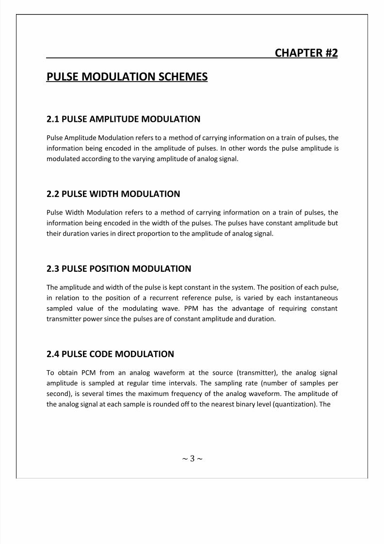
2.1 PULSE AMPLITUDE MODULATION
Pulse Amplitude Modulation refers to a method of carrying information on a train of pulses, the
information being encoded in the amplitude of pulses. In other words the pulse amplitude is
modulated according to the varying amplitude of analog signal.
2.2 PULSE WIDTH MODULATION
Pulse Width Modulation refers to a method of carrying information on a train of pulses, the
information being encoded in the width of the pulses. The pulses have constant amplitude but
their duration varies in direct proportion to the amplitude of analog signal.
2.3 PULSE POSITION MODULATION
The amplitude and width of the pulse is kept constant in the system. The position of each pulse,
in relation to the position of a recurrent reference pulse, is varied by each instantaneous
sampled value of the modulating wave. PPM has the advantage of requiring constant
transmitter power since the pulses are of constant amplitude and duration.
2.4 PULSE CODE MODULATION
To obtain PCM from an analog waveform at the source (transmitter), the analog signal
amplitude is sampled at regular time intervals. The sampling rate (number of samples per
second), is several times the maximum frequency of the analog waveform. The amplitude of
the analog signal at each sample is rounded off to the nearest binary level (quantization). The
8/13/2019 Inverter,design inverter
http://slidepdf.com/reader/full/inverterdesign-inverter 11/51
~ 4 ~
Figure 1(a) Analog signal, s(t ). (b) Pulse-amplitude modulation. (c) Pulse-width modulation.
(d ) Pulse position modulation
Number of levels is always a power of 2 (4, 8, 16, 32, 64, ...). These numbers can be represented
by two, three, four, five, six or more binary digits.
PCM is a general scheme for transmitting analog data in a digital and binary way, independent
of the complexity of the analog waveform. With PCM all forms of analog data like video, voice,
music and telemetry can be transferred.
2.6 ADVANTAGES OF PWM
The output voltage control is easier with PWM than other schemes and can be achieved
without any additional components. The lower order harmonics are either minimized or eliminated altogether.
The filtering requirements are minimized as lower order harmonics are eliminated and
higher order harmonics are filtered easily.
It has very low power consumption.
The entire control circuit can be digitized which reduces the susceptibility of the circuit
to interference.
8/13/2019 Inverter,design inverter
http://slidepdf.com/reader/full/inverterdesign-inverter 12/51
~ 5 ~
CHAPTER #3
PULSE WIDTH MODULATION
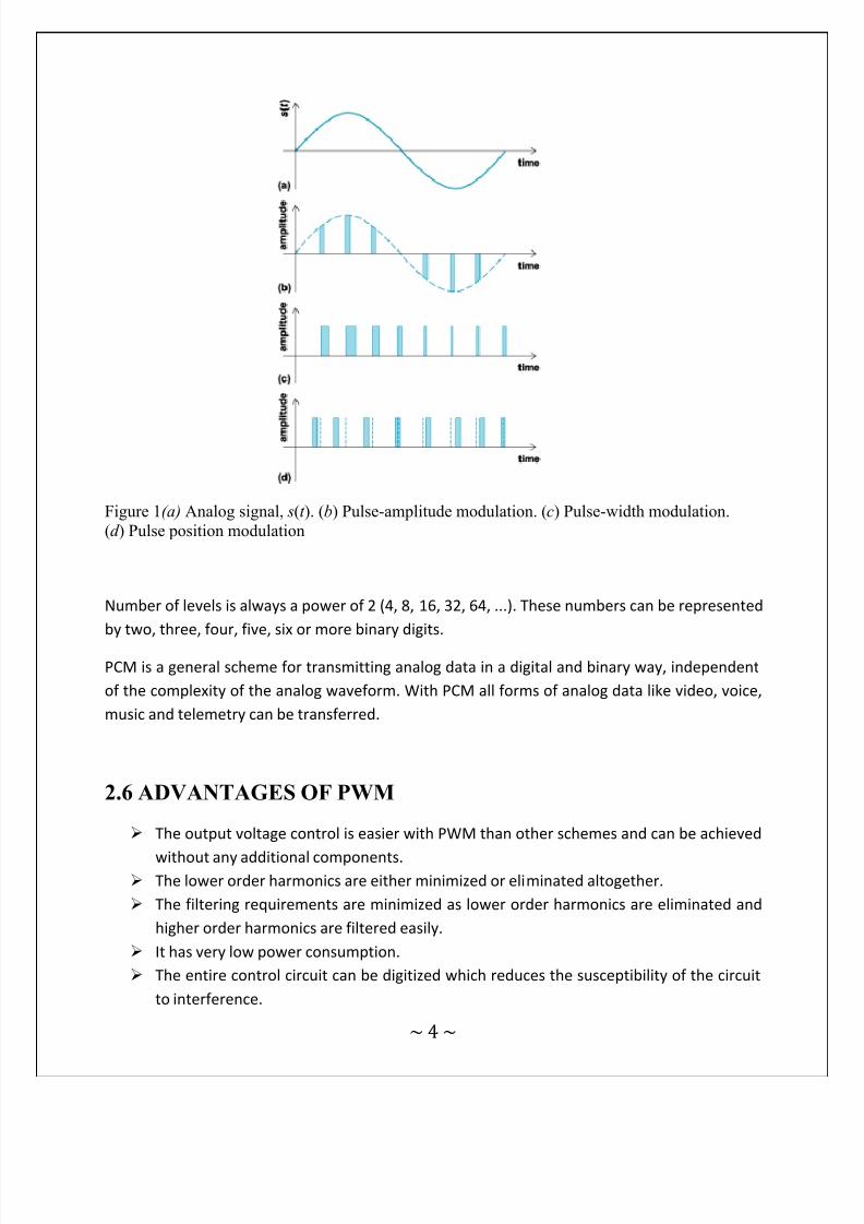
PWM is the most popular method for producing a controlled output for inverters. They are
quite popular in industrial applications.
Figure2 (sine modulated, unmodulated signal)
3.1 LINEAR MODULATION
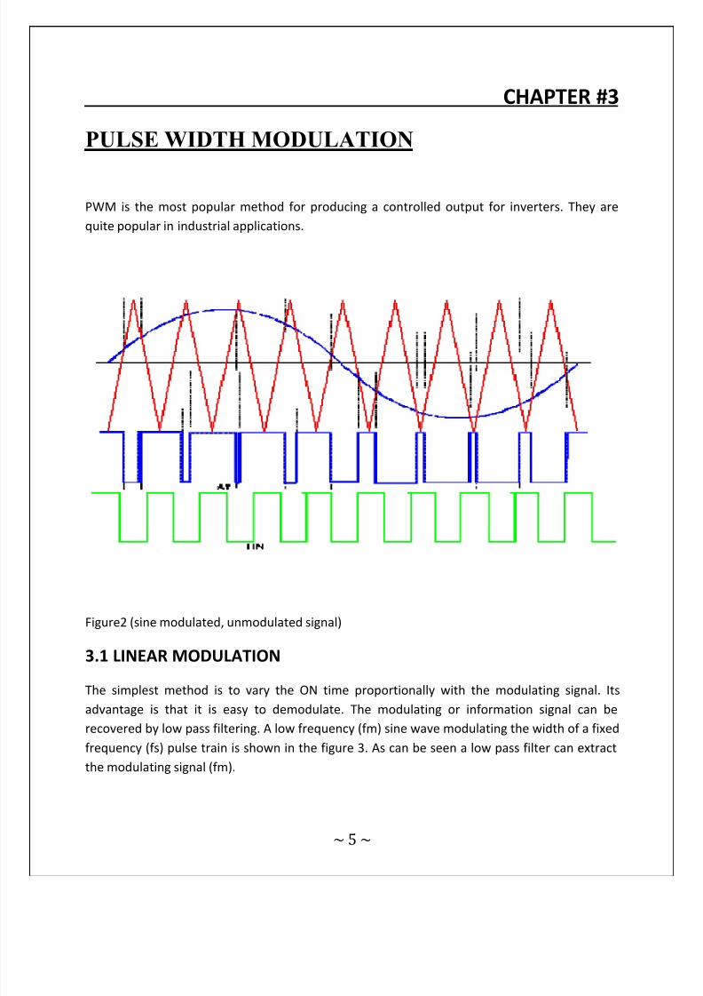
The simplest method is to vary the ON time proportionally with the modulating signal. Its
advantage is that it is easy to demodulate. The modulating or information signal can be
recovered by low pass filtering. A low frequency (fm) sine wave modulating the width of a fixed
frequency (fs) pulse train is shown in the figure 3. As can be seen a low pass filter can extract
the modulating signal (fm).
8/13/2019 Inverter,design inverter
http://slidepdf.com/reader/full/inverterdesign-inverter 13/51
~ 6 ~
Figure 3.
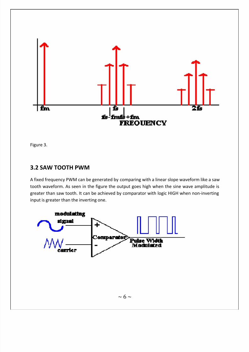
3.2 SAW TOOTH PWM
A fixed frequency PWM can be generated by comparing with a linear slope waveform like a saw
tooth waveform. As seen in the figure the output goes high when the sine wave amplitude is
greater than saw tooth. It can be achieved by comparator with logic HIGH when non-inverting
input is greater than the inverting one.
8/13/2019 Inverter,design inverter
http://slidepdf.com/reader/full/inverterdesign-inverter 14/51
~ 7 ~
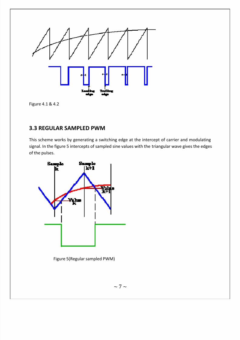
Figure 4.1 & 4.2
3.3 REGULAR SAMPLED PWM
This scheme works by generating a switching edge at the intercept of carrier and modulating
signal. In the figure 5 intercepts of sampled sine values with the triangular wave gives the edges
of the pulses.
Figure 5(Regular sampled PWM)

8/13/2019 Inverter,design inverter
http://slidepdf.com/reader/full/inverterdesign-inverter 15/51
~ 8 ~
CHAPTER #4
SINGLE PHASE PWM INVERTERS
In many industrial applications, to control the output voltage of the inverters is necessary for
the following reasons
To adjust with variations of dc input voltage
To regulate voltage of inverters
To satisfy the contain volts and frequency control requirement
There are various techniques to vary the inverter gain. The most efficient method of Controlling
the gain (and output voltage) is to incorporate pulse width modulation (PWM) Control within
the inverters. The commonly used techniques are
a) Single Pulse width Modulation
b) Multiple Pulse width Modulation
c) Sinusoidal Pulse width Modulation
d) Modified sinusoidal Pulse width Modulation
e) Phase-displacement control.
The PWM techniques given above vary with respect to the harmonic content in their output
voltages.
4.1 SINGLE PULSE WIDTH MODULATION
In this control, there’s only one pulse per half cycle and the width of the pulse is varied to control the
inverter output. The gating signals are generated by comparing a rectangular reference signal of the
amplitude Ar with triangular carrier wave of amplitude Ac, the frequency of the carrier wave determinesthe fundamental frequency of output voltage. By varying Ar from 0 to Ac ,the pulse width can be varied
from 0 to 100 percent. The ratio of Ar to Ac is the control variable and defined as the modulation index.

8/13/2019 Inverter,design inverter
http://slidepdf.com/reader/full/inverterdesign-inverter 16/51
~ 9 ~
4.2 MULTIPLE PULSE WIDTH MODULATION
The harmonic content can be reduced by using several pulses in each half cycle of output
voltage. The generation of gating signals for turning ON and OFF transistors by comparing a
reference signal with a triangular carrier wave. The frequency F c, determines the number of
pulses per half cycle. The modulation index controls the output voltage. This type of modulationis also known as uniform pulse width modulation (UPWM).
4.3 SINUSOIDAL PULSE WIDTH MODULATION
Instead of, maintaining the width of all pulses of same as in case of multiple pulse width
modulation, the width of each pulse is varied in proportion to the amplitude of a sine wave
evaluated at the centre of the same pulse. The distortion factor and lower order harmonics arereduced significantly. The gating signals are generated by comparing a sinusoidal reference
signal with a triangular carrier wave of frequency Fc. The frequency of reference signal Fr
,determines the inverter output frequency and its peak amplitude Ar, controls the modulation
index M, and rms output voltage Vo. The number of pulses per half cycle depends on carrier
frequency .
8/13/2019 Inverter,design inverter
http://slidepdf.com/reader/full/inverterdesign-inverter 17/51
~ 10 ~
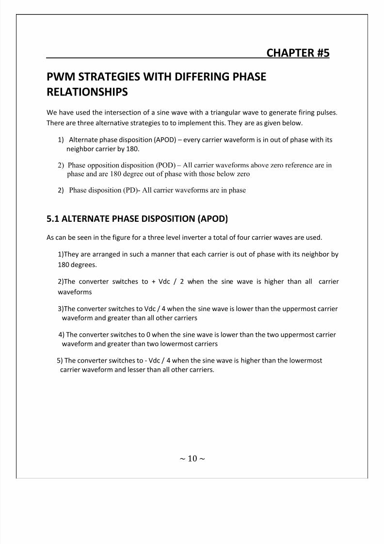
CHAPTER #5
PWM STRATEGIES WITH DIFFERING PHASE
RELATIONSHIPSWe have used the intersection of a sine wave with a triangular wave to generate firing pulses.
There are three alternative strategies to to implement this. They are as given below.
1) Alternate phase disposition (APOD) – every carrier waveform is in out of phase with its
neighbor carrier by 180.
2) Phase opposition disposition (POD) – All carrier waveforms above zero reference are in
phase and are 180 degree out of phase with those below zero
2) Phase disposition (PD)- All carrier waveforms are in phase
5.1 ALTERNATE PHASE DISPOSITION (APOD)
As can be seen in the figure for a three level inverter a total of four carrier waves are used.
1)They are arranged in such a manner that each carrier is out of phase with its neighbor by
180 degrees.
2)The converter switches to + Vdc / 2 when the sine wave is higher than all carrier
waveforms
3)The converter switches to Vdc / 4 when the sine wave is lower than the uppermost carrier
waveform and greater than all other carriers
4) The converter switches to 0 when the sine wave is lower than the two uppermost carrier
waveform and greater than two lowermost carriers
5) The converter switches to - Vdc / 4 when the sine wave is higher than the lowermost
carrier waveform and lesser than all other carriers.
8/13/2019 Inverter,design inverter
http://slidepdf.com/reader/full/inverterdesign-inverter 18/51
~ 11 ~
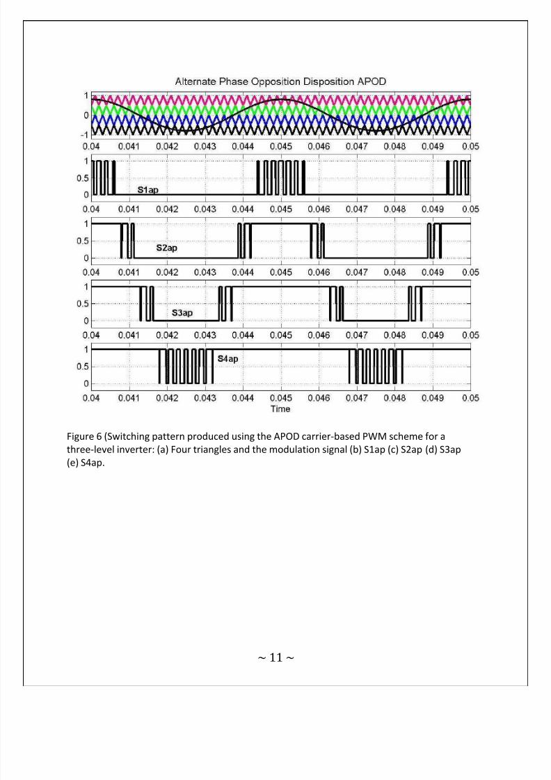
Figure 6 (Switching pattern produced using the APOD carrier-based PWM scheme for a
three-level inverter: (a) Four triangles and the modulation signal (b) S1ap (c) S2ap (d) S3ap
(e) S4ap.
8/13/2019 Inverter,design inverter
http://slidepdf.com/reader/full/inverterdesign-inverter 19/51
~ 12 ~
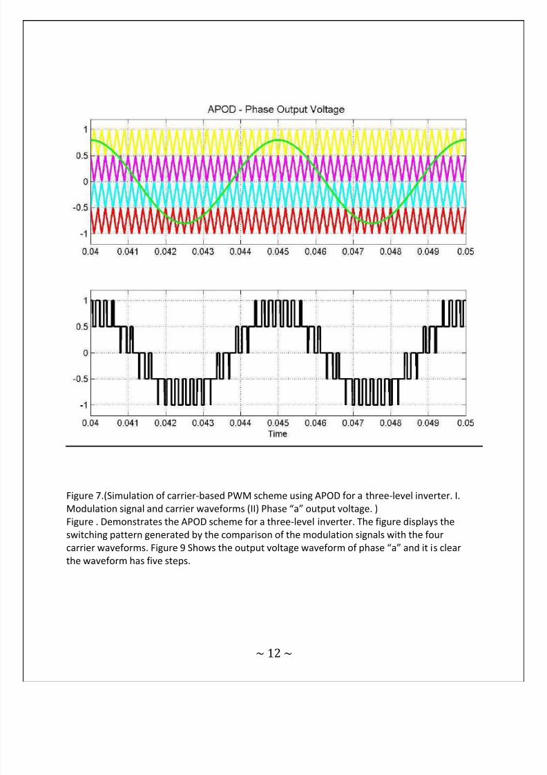
Figure 7.(Simulation of carrier-based PWM scheme using APOD for a three-level inverter. I.
Modulation signal and carrier waveforms (II) Phase “a” output voltage. )
Figure . Demonstrates the APOD scheme for a three-level inverter. The figure displays the
switching pattern generated by the comparison of the modulation signals with the four
carrier waveforms. Figure 9 Shows the output voltage waveform of phase “a” and it is clear
the waveform has five steps.

8/13/2019 Inverter,design inverter
http://slidepdf.com/reader/full/inverterdesign-inverter 20/51
~ 13 ~
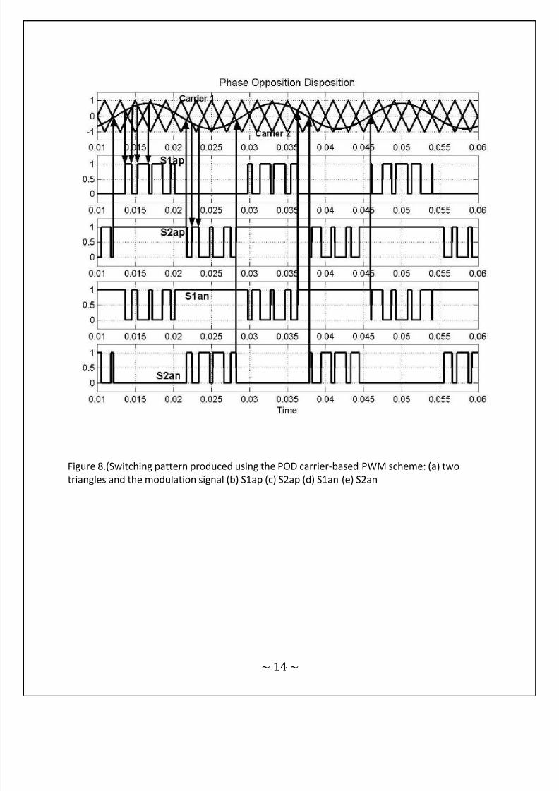
5.2 PHASE OPPOSITION DISPOSITION (POD)
The rules for the two level inverter
1) Two carrier waveforms are arranged so that all carrier waveforms above zero are in
phase and are 180 degrees out of phase with those below zero
2) The converter is switched to + Vdc / 2 when the sine wave is higher than both carrier
waveforms
3) The converter is switched to zero when the sine wave is greater than the lower carrier
waveform but less than the upper carrier waveform
4) The converter is switched to - Vdc / 2 when the sine wave is less than both carrier
waveforms
As seen from Figure, the figure illustrates the switching functions produced by POD carrier
based PWM scheme. In the PWM scheme there are two triangles, upper triangle magnitude
from 1 to 0 and the lower triangle from 0 to –1 and these two triangle waveforms are in out of
phase.
When the modulation signal is greater than both the carrier waveforms, S1ap and S2ap are
turned on and the converter switches to positive node voltage and when the reference is less
than the upper carrier waveform but greater than the lower carrier, S2ap and S1an are turned
on and the converter switches to neutral point. When the reference is lower than both carrier
waveforms, S1an and S2an are turned on and the converter switches to negative node voltage.
8/13/2019 Inverter,design inverter
http://slidepdf.com/reader/full/inverterdesign-inverter 21/51
~ 14 ~
Figure 8.(Switching pattern produced using the POD carrier-based PWM scheme: (a) two
triangles and the modulation signal (b) S1ap (c) S2ap (d) S1an (e) S2an
8/13/2019 Inverter,design inverter
http://slidepdf.com/reader/full/inverterdesign-inverter 22/51
~ 15 ~
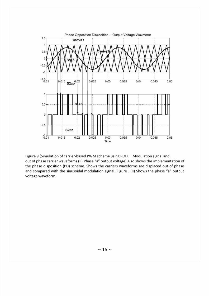
Figure 9.(Simulation of carrier-based PWM scheme using POD. I. Modulation signal andout of phase carrier waveforms (II) Phase “a” output voltage) Also shows the implementation of
the phase disposition (PD) scheme. Shows the carriers waveforms are displaced out of phase
and compared with the sinusoidal modulation signal. Figure . (II) Shows the phase “a” output
voltage waveform.

8/13/2019 Inverter,design inverter
http://slidepdf.com/reader/full/inverterdesign-inverter 23/51
~ 16 ~
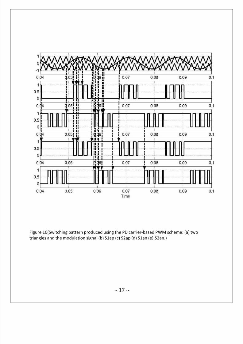
5.3 PHASE DISPOSITION (PD)
The rules for phase disposition method for a two level inverter are
1) 2 carrier waveforms in phase are arranged.
2) The converter is switched to + Vdc / 2 when the sine wave is greater than both carrier
waveform
3)The converter is switched to zero when sine wave is lower than upper carrier but higher
than the lower carrier
4) The converter is switched to - Vdc / 2 when the sine wave is less than both carrier
waveforms
As can be seen from the figure in the PWM scheme there are two triangles, the upper triangle
ranges from 1 to 0 and the lower triangle ranges from 0 to –1. During the positive cycle of the
modulation signal, when the modulation is greater than Triangle 1 and Triangle 2, then S1ap
and S2ap are turned on and also during the positive cycle S2ap is completely turned on. When
S1ap and S2ap are turned on the converter switches to the + Vdc / 2 and when S1an and S2ap
are on, the converter switches to zero and hence during the positive cycle S2ap is completely
turned on and S1ap and S1an will be turning on and off and hence the converter switches from
+ Vdc / 2 to 0. During the negative half cycle of the modulation signal the converter switches
from 0 to -Vdc / 2.
8/13/2019 Inverter,design inverter
http://slidepdf.com/reader/full/inverterdesign-inverter 24/51
~ 17 ~
Figure 10(Switching pattern produced using the PD carrier-based PWM scheme: (a) two
triangles and the modulation signal (b) S1ap (c) S2ap (d) S1an (e) S2an.)
8/13/2019 Inverter,design inverter
http://slidepdf.com/reader/full/inverterdesign-inverter 25/51
~ 18 ~
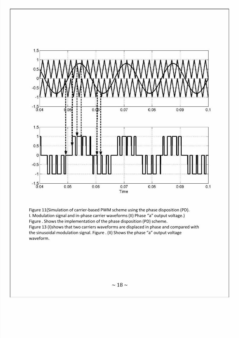
Figure 11(Simulation of carrier-based PWM scheme using the phase disposition (PD).
I. Modulation signal and in-phase carrier waveforms (II) Phase “a” output voltage.)
Figure . Shows the implementation of the phase disposition (PD) scheme.
Figure 13 (I)shows that two carriers waveforms are displaced in phase and compared with
the sinusoidal modulation signal. Figure . (II) Shows the phase “a” output voltage
waveform.

8/13/2019 Inverter,design inverter
http://slidepdf.com/reader/full/inverterdesign-inverter 26/51
~ 19 ~
CHAPTER#6
APPLICATIONS IN HARMONIC ELIMINATION
The present chapter helps us to understand the effects of non-linear loads on the power system
and the implementation of suitable devices to cancel out the harmonics. The use of inverters in active
power filters has been emphasized and the simulated circuits and results have been described in
particular.
6.1 NON LINEAR LOADS
A non-linear load on a power system is typically a rectifier or some kind of arc discharge device such as a
fluorescent lamp, electric welding machine, or arc furnace in which current is not linearly related to the voltage.
Because current in these systems is interrupted by a switching action, the current contains frequency
components that are multiples of the power system frequency. This leads to distortion of the current waveform
which in turn distorts the voltage waveform. Distortion power factor is a measure of how much the harmonic
distortion of a load current decreases the average power transferred to the load.
6.2 ACTIVE POWER FILTERS
The increasing use of power electronics based loads (adjustable speed drives, switch mode power
supplies, etc.) to improve system efficiency and controllability is increasing the concern for harmonic
distortion levels in end use facilities and on the overall power system. The application of passive
tuned filters creates new system resonances which are dependent on specific system conditions.
In general, passive tuned filters have been used to minimize low-frequency current
harmonics while high-pass units have been connected to attenuate the amplitude of high frequency
current components. However, high-pass filters present disadvantages due to the resistance
connected in parallel to the inductor, which increases the filter losses and reduces the filtering
effectiveness at the tuned frequency. The most critical aspects of passive filters are related to the fact
that they cannot modify their compensation characteristics following the dynamic changes of the
nonlinear load, the performance dependence they present with the power system parameters, and
the probability of series resonances with the power system’s equivalent reactance. Passive filter
ratings must be coordinated with reactive power requirements of the loads and it is often difficult to
design the filters to avoid leading power factor operation for some load conditions.
Also, the passive filter generates at fundamental frequency reactive power that changes the
system voltage regulation, and if the filter is not designed properly or disconnected during low load
operating conditions, over-voltages can be generated at its terminals.
A flexible and versatile solution to voltage/current quality problems is offered by active
power filters. Active filters have the advantage of being able to compensate for harmonics
8/13/2019 Inverter,design inverter
http://slidepdf.com/reader/full/inverterdesign-inverter 27/51
~ 20 ~
without fundamental frequency reactive power concerns. This means that the rating of the active
power can be less than a conquerable passive filter for the same nonlinear load and the active
filter will not introduce system resonances that can move a harmonic problem from one frequency
to another.
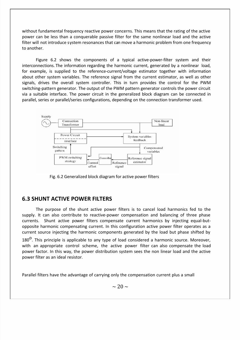
Figure 6.2 shows the components of a typical active-power-filter system and theirinterconnections. The information regarding the harmonic current, generated by a nonlinear load,
for example, is supplied to the reference-current/voltage estimator together with information
about other system variables. The reference signal from the current estimator, as well as other
signals, drives the overall system controller. This in turn provides the control for the PWM
switching-pattern generator. The output of the PWM pattern generator controls the power circuit
via a suitable interface. The power circuit in the generalized block diagram can be connected in
parallel, series or parallel/series configurations, depending on the connection transformer used.
Fig. 6.2 Generalized block diagram for active power filters
6.3 SHUNT ACTIVE POWER FILTERS
The purpose of the shunt active power filters is to cancel load harmonics fed to the
supply. It can also contribute to reactive-power compensation and balancing of three phase
currents. Shunt active power filters compensate current harmonics by injecting equal-but-
opposite harmonic compensating current. In this configuration active power filter operates as a
current source injecting the harmonic components generated by the load but phase shifted by
180o. This principle is applicable to any type of load considered a harmonic source. Moreover,
with an appropriate control scheme, the active power filter can also compensate the load
power factor. In this way, the power distribution system sees the non linear load and the active
power filter as an ideal resistor.
Parallel filters have the advantage of carrying only the compensation current plus a small

8/13/2019 Inverter,design inverter
http://slidepdf.com/reader/full/inverterdesign-inverter 28/51
~ 21 ~
amount of active fundamental current supplied to compensate for system losses. It is possible to
connect several filters in parallel to cater for higher currents, which makes this type of circuit
suitable for a wide range of power ratings.
6.4 MODELLING OF THREE WIRE SHUNT ACTIVE POWER FILTER
The concept of using active power filters to mitigate harmonic problems and to
compensate reactive power was proposed more than two decades ago [Akagi et al., 1984]. Since
then the theories and applications of active power filters have become more popular and have
attracted great attention. Without the drawbacks of passive harmonic filters, the active power
filter appears to be a viable solution for reactive power compensation as well as for eliminating
harmonic currents.
Active power filters are researched and developed as a viable alternative over the passive
filters and static var compensators to solve the problems of harmonics injection and reactive
power requirement of non-linear loads .Among the various topologies developed the shunt active
power filter based on the current controlled voltage source type PWM converter has proved to be
effective even when the load is highly non-linear.
The control strategies of the active filters are implemented mainly in three steps – Signal
conditioning, estimation of compensating signals and generation of firing signals for switching
devices. Estimation of compensating signal is the most important part of the active filter control. It
has a great impact on the compensating objectives, rating of active filters and its transient as well
as steady state performance. The control strategies use either frequency domain or time domain
approaches to extract compensating signals from the corresponding distorted currents/voltages.
6.5 SYSTEM DESCRIPTION
The active power filter uses power electronic switching to generate harmonic currents that
cancel the harmonic currents from a load. The active filter configuration investigated in this study
is based on a voltage source inverter that interfaces to the system through an interface reactor.
In this configuration, the filter is connected in parallel with the load being compensated.
Therefore the configuration is often referred to as a shunt (parallel) active filter. The approach is
based on the principle of injecting harmonic current into the AC system, of the same amplitude
and reverse phase to that of the load current harmonics. Figure6.5 shows the main components of
a typical active power filter system and their interconnections.
The main components of the system are :
(a) Mains supply (b) Non linear load (c) Active power filter
Active power filter – (i) voltage source inverter , (ii) interface reactor ,(iii) reference current
generator , (iv) current controller .
8/13/2019 Inverter,design inverter
http://slidepdf.com/reader/full/inverterdesign-inverter 29/51
~ 22 ~
Fig.6.5 System model with shunt active power filter
6.6 MAINS SUPPLY
Mains supply is a three phase 415V 50 Hz wye connected power supply with a grounded neutral
point equivalent of the actual system i.e. a three phase 3 wire system.
6.7 NON LINEAR LOAD
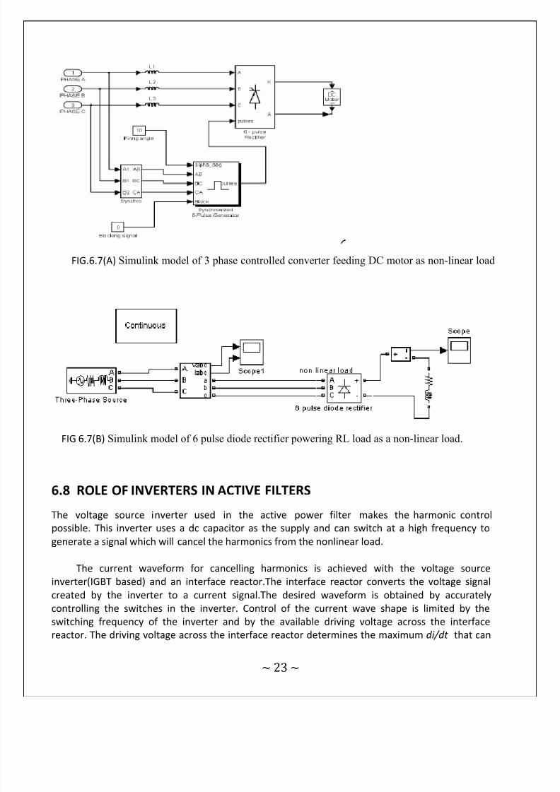
The nonlinear load block is a three-phase fully controlled bridge rectifier feeding a DC motor.
The DC motor is modeled with a resistance, inductance and a back emf. It is possible to control
the firing angle of the controlled three-phase rectifier. The Matlab/Simulink model of the
nonlinear load block is shown in Figure 6.7(A).
Another non-linear load can be a three phase six-pulse converter feeding a RL load. This model of
non-linear load has been used in the main model involving active power filters. The
MATLAB/SIMULINK models of both kinds of non-linear loads are shown below in fig. 6.7(B)
8/13/2019 Inverter,design inverter
http://slidepdf.com/reader/full/inverterdesign-inverter 30/51
~ 23 ~
FIG.6.7(A) Simulink model of 3 phase controlled converter feeding DC motor as non-linear load
FIG 6.7(B) Simulink model of 6 pulse diode rectifier powering RL load as a non-linear load.
6.8 ROLE OF INVERTERS IN ACTIVE FILTERS
The voltage source inverter used in the active power filter makes the harmonic control
possible. This inverter uses a dc capacitor as the supply and can switch at a high frequency to
generate a signal which will cancel the harmonics from the nonlinear load.
The current waveform for cancelling harmonics is achieved with the voltage source
inverter(IGBT based) and an interface reactor.The interface reactor converts the voltage signal
created by the inverter to a current signal.The desired waveform is obtained by accurately
controlling the switches in the inverter. Control of the current wave shape is limited by the
switching frequency of the inverter and by the available driving voltage across the interface
reactor. The driving voltage across the interface reactor determines the maximum di/dt that can
8/13/2019 Inverter,design inverter
http://slidepdf.com/reader/full/inverterdesign-inverter 31/51
~ 24 ~
be achieved by the power filter. This is important because relatively high values of di/dt may be
needed to cancel higher order harmonic components.
The voltage source inverter is the heart of the active power filter. In the system model of the
project it has been modelled as a three phase ,full wave inverter (IGBT based). Each of the three
identical inverter legs consisted of two IGBT and two anti-parallel diodes. The igbt used here ismodelled in the simulink as a resistor (Ron) and inductor(Lon) in series with a switch(transistor)
controlled by a logical signal. It switches between on and off state instantaneously when
triggered.
6.9 INTERFACE REACTOR
The interface reactor provides the isolation and filtering between the output of the
voltage source inverter and the power system where the active power filter is connected. The
inductance allows the output of the active power filter to look like a current source to the power
system. The inductance makes it possible to charge the dc capacitor to a voltage greater than theac line-to-line peak voltage. The inductance also functions like a commutation impedance. It limits
the magnitude of a current spike during commutation and prevents the switching device from
seeing an excessive rate of current change. Besides these, it is not possible to connect a
sinusoidal voltage supply to the non-sinusoidal output of the voltage source inverter without a
reactor. Sizing of the reactor value must take into account control of the inverter switching
frequencies and the characteristics of the nonlinear load to be compensated.
6.10 REFERENCE CURRENT GENERATIONIn this shunt active power filter, control is accomplished by monitoring the three phase line
currents to the nonlinear load and the three phase line-to-neutral voltages at the load bus, and
then generating the three phase reference currents that should be supplied by the voltage source
inverter. In this simulation study compensating current reference signal is derived from the measured
quantities by the use of the Instantaneous Reactive Power Theory based method. The general
definitions of active and reactive power have been presented in references [Akagi et al., 1984, Akagi
et al., 1986]. In this formulation, active and reactive powers are expressed as the dot and cross
product of voltage and current vectors. Once the compensating currents are detected, they are used
as a reference signal in the inverter current control loop and thus compared with the real voltage
source inverter current to generate the switching control signals. To deal with instantaneous voltagesand currents in three-phase circuits mathematically, it is adequate to express their quantities as the
instantaneous space vectors. For simplicity the three phase voltages and currents excluding zero-
phase sequence components will be considered i.e. three phase 3 wire systems.
In a, b, c coordinates, the a, b and c axes are fixed on the same plane, apart from each other by
2π/3. The instantaneous space vectors eα and iα are set on the α- axis and their amplitude and
8/13/2019 Inverter,design inverter
http://slidepdf.com/reader/full/inverterdesign-inverter 32/51
~ 25 ~
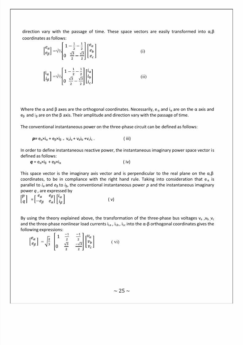
direction vary with the passage of time. These space vectors are easily transformed into α,β
coordinates as follows:
=√⅔ (i)
=√⅔ (ii)
Where the α and β axes are the orthogonal coordinates. Necessarily, e α and iα are on the α axis and
eβ and iβ are on the β axis. Their amplitude and direction vary with the passage of time.
The conventional instantaneous power on the three-phase circuit can be defined as follows:
p= eα×iα + eβ×iβ = vaia + vbib +vcic . ( iii)
In order to define instantaneous reactive power, the instantaneous imaginary power space vector is
defined as follows:
q = eα×iβ + eβ×iα ( iv)
This space vector is the imaginary axis vector and is perpendicular to the real plane on the α,β
coordinates, to be in compliance with the right hand rule. Taking into consideration that e α isparallel to i α and eβ to i β, the conventional instantaneous power p and the instantaneous imaginary
power q , are expressed by
= ( v)
By using the theory explained above, the transformation of the three-phase bus voltages va ,vb ,vc
and the three-phase nonlinear load currents iLa , iLb , iLc into the α-β orthogonal coordinates gives the
following expressions:
= ( vi)
8/13/2019 Inverter,design inverter
http://slidepdf.com/reader/full/inverterdesign-inverter 33/51
~ 26 ~
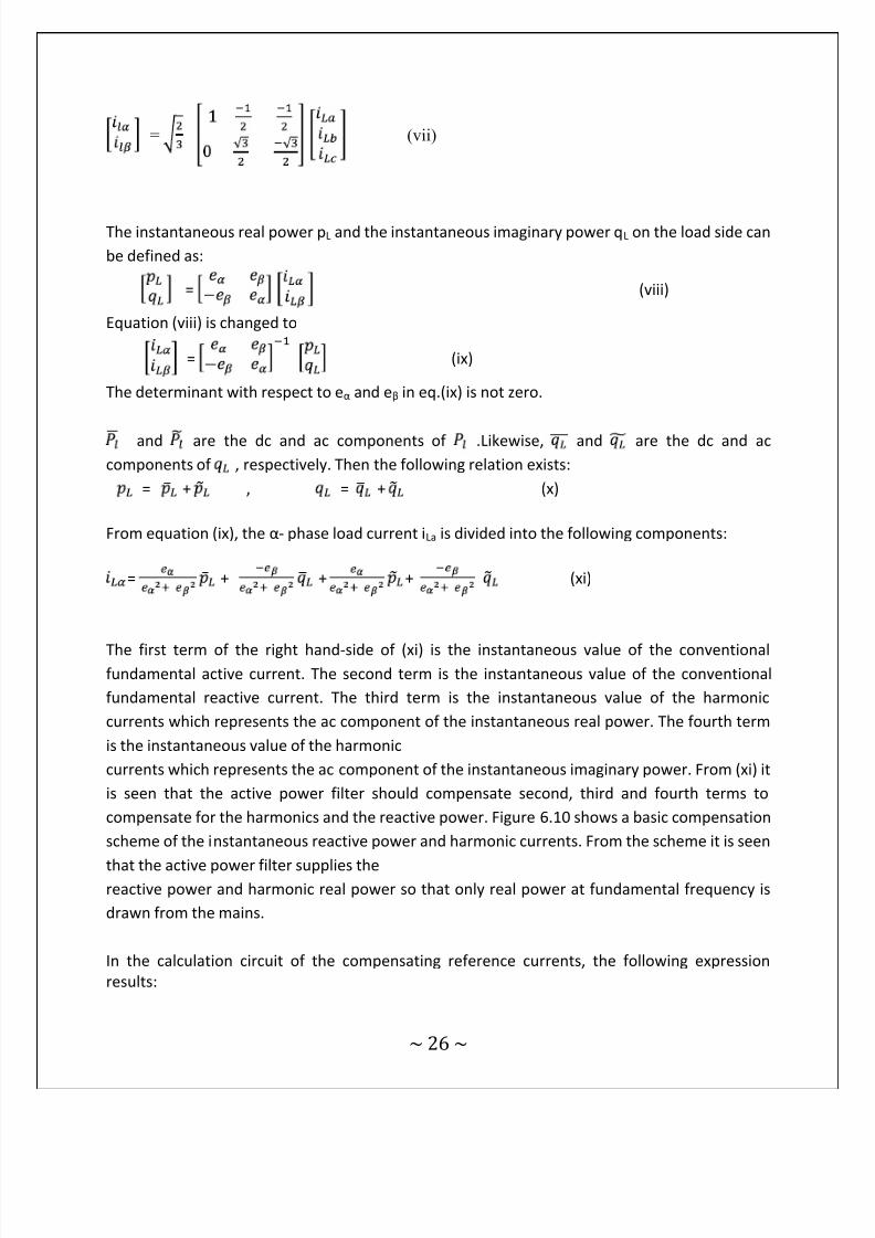
= (vii)
The instantaneous real power pL and the instantaneous imaginary power qL on the load side can
be defined as:
= (viii)
Equation (viii) is changed to
= (ix)
The determinant with respect to eα and eβ in eq.(ix) is not zero.
and are the dc and ac components of .Likewise, and are the dc and ac
components of , respectively. Then the following relation exists:
= + , = + (x)
From equation (ix), the α- phase load current iLa is divided into the following components:
= + + + (xi)
The first term of the right hand-side of (xi) is the instantaneous value of the conventionalfundamental active current. The second term is the instantaneous value of the conventional
fundamental reactive current. The third term is the instantaneous value of the harmonic
currents which represents the ac component of the instantaneous real power. The fourth term
is the instantaneous value of the harmonic
currents which represents the ac component of the instantaneous imaginary power. From (xi) it
is seen that the active power filter should compensate second, third and fourth terms to
compensate for the harmonics and the reactive power. Figure 6.10 shows a basic compensation
scheme of the instantaneous reactive power and harmonic currents. From the scheme it is seen
that the active power filter supplies thereactive power and harmonic real power so that only real power at fundamental frequency is
drawn from the mains.
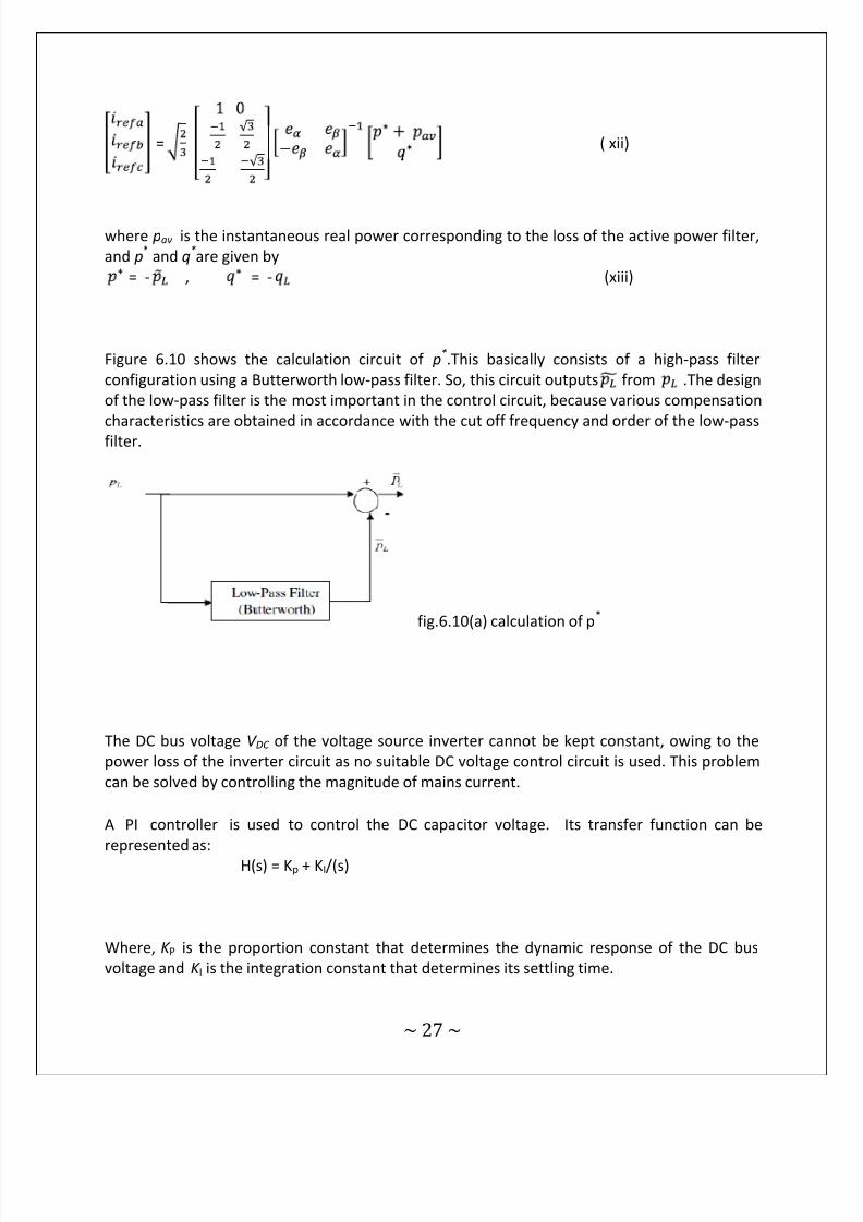
In the calculation circuit of the compensating reference currents, the following expression
results:
8/13/2019 Inverter,design inverter
http://slidepdf.com/reader/full/inverterdesign-inverter 34/51
~ 27 ~
= ( xii)
where pav is the instantaneous real power corresponding to the loss of the active power filter,
and p* and q
*are given by
= - , = - (xiii)
Figure 6.10 shows the calculation circuit of p*.This basically consists of a high-pass filter
configuration using a Butterworth low-pass filter. So, this circuit outputs from .The design
of the low-pass filter is the most important in the control circuit, because various compensation
characteristics are obtained in accordance with the cut off frequency and order of the low-passfilter.
fig.6.10(a) calculation of p*
The DC bus voltage V DC of the voltage source inverter cannot be kept constant, owing to the
power loss of the inverter circuit as no suitable DC voltage control circuit is used. This problem
can be solved by controlling the magnitude of mains current.
A PI controller is used to control the DC capacitor voltage. Its transfer function can be
represented as:
H(s) = Kp + KI/(s)
Where, K P is the proportion constant that determines the dynamic response of the DC bus
voltage and K I is the integration constant that determines its settling time.
8/13/2019 Inverter,design inverter
http://slidepdf.com/reader/full/inverterdesign-inverter 35/51
~ 28 ~
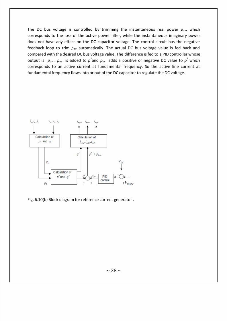
The DC bus voltage is controlled by trimming the instantaneous real power pav , which
corresponds to the loss of the active power filter, while the instantaneous imaginary power
does not have any effect on the DC capacitor voltage. The control circuit has the negative
feedback loop to trim pav automatically. The actual DC bus voltage value is fed back and
compared with the desired DC bus voltage value. The difference is fed to a PID controller whoseoutput is pav . pav is added to p
*and pav adds a positive or negative DC value to p
*which
corresponds to an active current at fundamental frequency. So the active line current at
fundamental frequency flows into or out of the DC capacitor to regulate the DC voltage.
Fig. 6.10(b) Block diagram for reference current generator .
8/13/2019 Inverter,design inverter
http://slidepdf.com/reader/full/inverterdesign-inverter 36/51
~ 29 ~
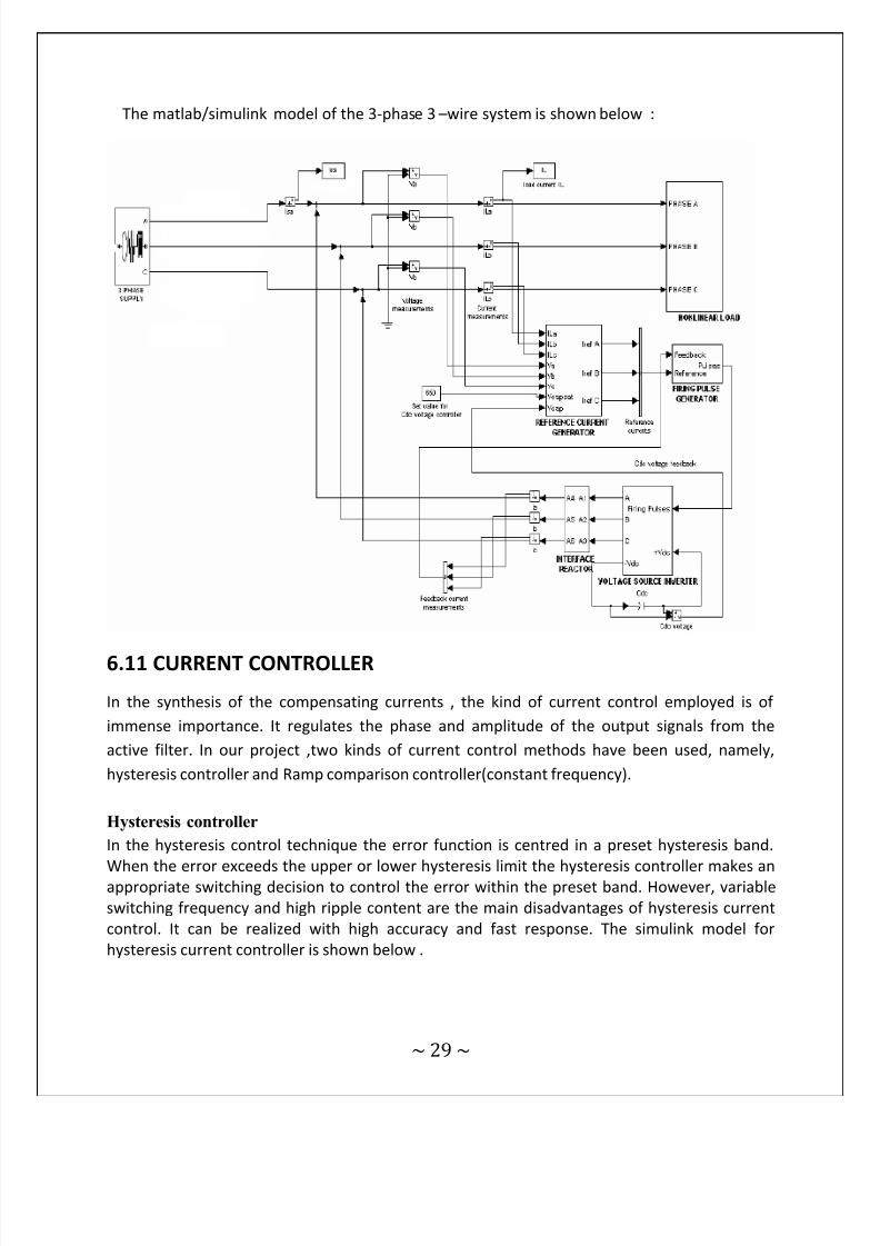
The matlab/simulink model of the 3-phase 3 –wire system is shown below :
6.11 CURRENT CONTROLLER
In the synthesis of the compensating currents , the kind of current control employed is of
immense importance. It regulates the phase and amplitude of the output signals from the
active filter. In our project ,two kinds of current control methods have been used, namely,
hysteresis controller and Ramp comparison controller(constant frequency).
Hysteresis controller
In the hysteresis control technique the error function is centred in a preset hysteresis band.
When the error exceeds the upper or lower hysteresis limit the hysteresis controller makes an appropriate switching decision to control the error within the preset band. However, variable
switching frequency and high ripple content are the main disadvantages of hysteresis current
control. It can be realized with high accuracy and fast response. The simulink model for
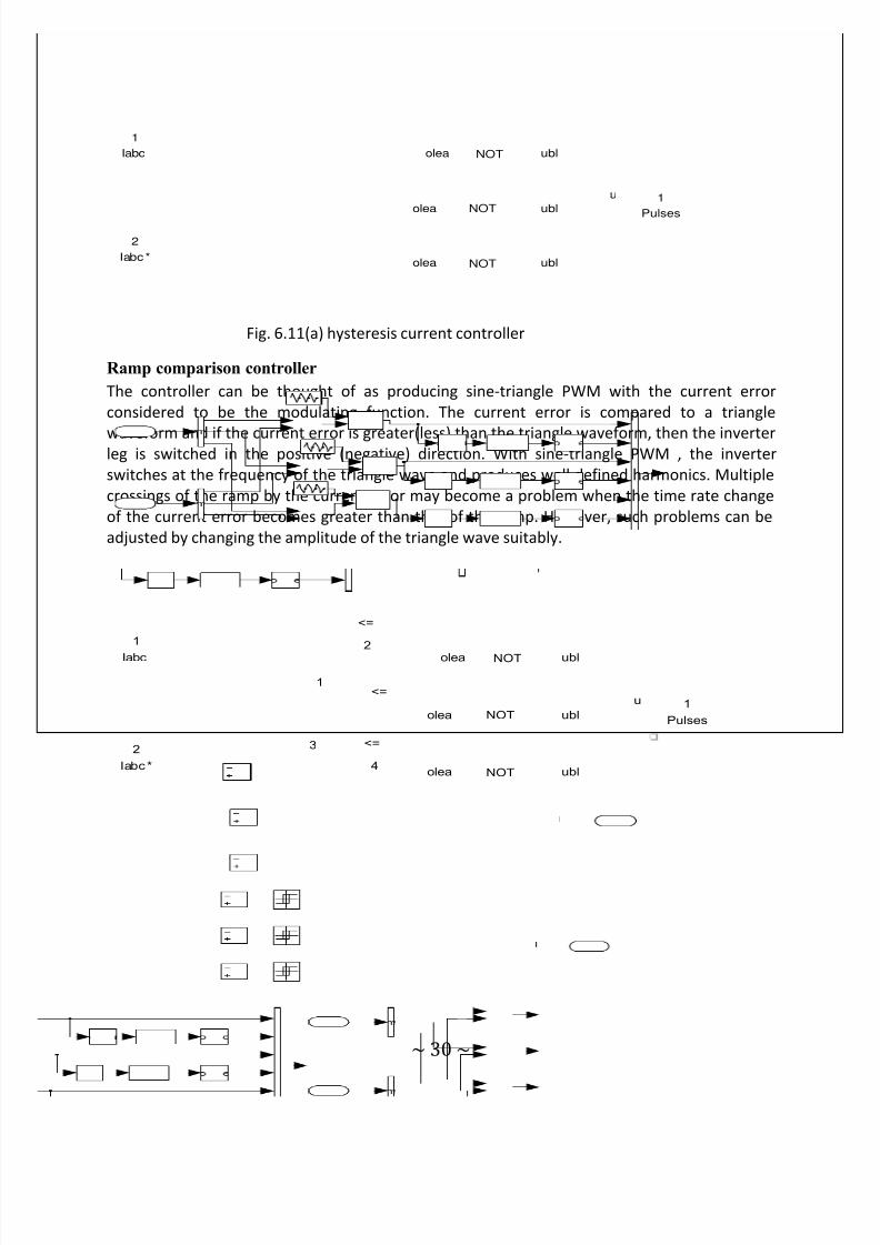
hysteresis current controller is shown below .
8/13/2019 Inverter,design inverter
http://slidepdf.com/reader/full/inverterdesign-inverter 37/51
~ 30 ~
Fig. 6.11(a) hysteresis current controller
Ramp comparison controller
The controller can be thought of as producing sine-triangle PWM with the current error
considered to be the modulating function. The current error is compared to a triangle
waveform and if the current error is greater(less) than the triangle waveform, then the inverterleg is switched in the positive (negative) direction. With sine-triangle PWM , the inverter
switches at the frequency of the triangle wave and produces well defined harmonics. Multiple
crossings of the ramp by the current error may become a problem when the time rate change
of the current error becomes greater than that of the ramp. However, such problems can be
adjusted by changing the amplitude of the triangle wave suitably.
Fig.6.11(b) ramp comparison controller
6.12 SIMULATION RESULTS
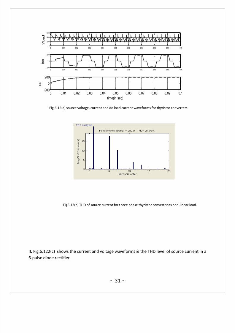
I. Fig.6.12(a) shows the voltage , current waveforms of a load fed by 3-phase thyristor
converter (at firing angle 45 ). The source current Isa is also shown. The effect of non-
linear loads is clearly observed.
Pulses
1u
NOT
NOT
NOT
olea
olea
ubl
ubl
ublolea
Iabc *
2
Iabc
1
Pulses
1u
NOT
NOT
NOT
olea
olea
ubl
ubl
ublolea
4
<=3
2
<=
1<=
Iabc*
2
Iabc
1
8/13/2019 Inverter,design inverter
http://slidepdf.com/reader/full/inverterdesign-inverter 38/51
~ 31 ~
Fig.6.12(a) source voltage, current and dc load current waveforms for thyristor converters.
Fig6.12(b) THD of source current for three phase thyristor converter as non-linear load.
II. Fig.6.122(c) shows the current and voltage waveforms & the THD level of source current in a
6-pulse diode rectifier.
0 0.01 0.02 0.03 0.04 0.05 0.06 0.07 0.08 0.09 0.10
200
400
600
V l o a d
0 0.01 0.02 0.03 0.04 0.05 0.06 0.07 0.08 0.09 0.1-200
0
200
I s a
0 0.01 0.02 0.03 0.04 0.05 0.06 0.07 0.08 0.09 0.1-200
0
200
time(in sec)
I d c
8/13/2019 Inverter,design inverter
http://slidepdf.com/reader/full/inverterdesign-inverter 39/51
~ 32 ~
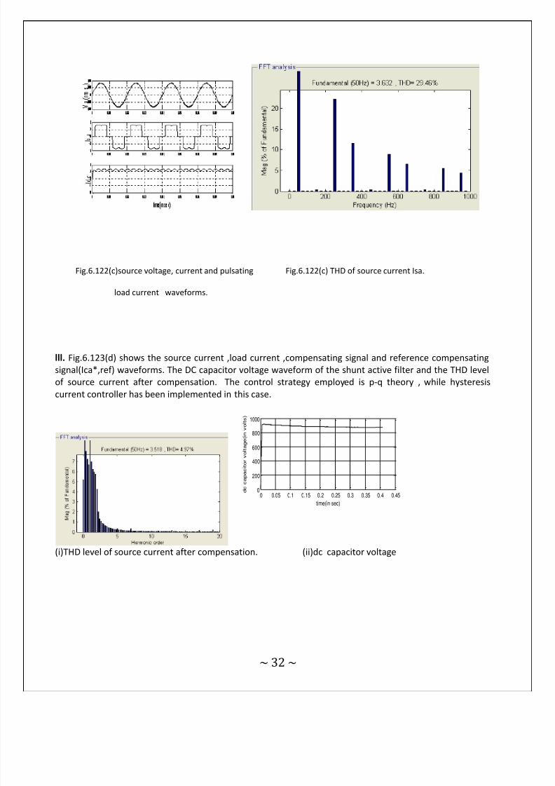
Fig.6.122(c)source voltage, current and pulsating Fig.6.122(c) THD of source current Isa.
load current waveforms.
lll. Fig.6.123(d) shows the source current ,load current ,compensating signal and reference compensating
signal(Ica*,ref) waveforms. The DC capacitor voltage waveform of the shunt active filter and the THD level
of source current after compensation. The control strategy employed is p-q theory , while hysteresis
current controller has been implemented in this case.
(i)THD level of source current after compensation. (ii)dc capacitor voltage
0 0.05 0.1 0.15 0.2 0.25 0.3 0.35 0.4 0.450
200
400
600
800
1000
time(in sec)
d c c a p a c i t o r v o l t a g e ( i n v o l t s )
8/13/2019 Inverter,design inverter
http://slidepdf.com/reader/full/inverterdesign-inverter 40/51
~ 33 ~
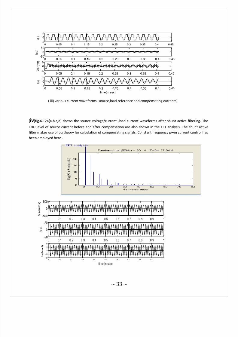
( iii) various current waveforms (source,load,reference and compensating currents)
(iv)fig.6.124(a,b,c,d) shows the source voltage/current ,load current waveforms after shunt active filtering. The
THD level of source current before and after compensation are also shown in the FFT analysis. The shunt active
filter makes use of pq theory for calculation of compensating signals. Constant frequency pwm current control has
been employed here .
0 0.05 0.1 0.15 0.2 0.25 0.3 0.35 0.4 0.45-5
0
5
i L a
0 0.05 0.1 0.15 0.2 0.25 0.3 0.35 0.4 0.45
-50
0
50
I c a *
0 0.05 0.1 0.15 0.2 0.25 0.3 0.35 0.4 0.45-5
0
5
I c a * ( r e f )
0 0.05 0.1 0.15 0.2 0.25 0.3 0.35 0.4 0.45-5
0
5
time(in sec)
I s a
0 0.1 0.2 0.3 0.4 0.5 0.6 0.7 0.8 0.9 1-500
0
500
V s a ( r m s )
0 0.1 0.2 0.3 0.4 0.5 0.6 0.7 0.8 0.9 1-20
0
20
I s a
0 0.1 0.2 0.3 0.4 0.5 0.6 0.7 0.8 0.9 1-20
-10
0
10
20
time(in sec)
I a ( l o a d )
8/13/2019 Inverter,design inverter
http://slidepdf.com/reader/full/inverterdesign-inverter 41/51
~ 34 ~
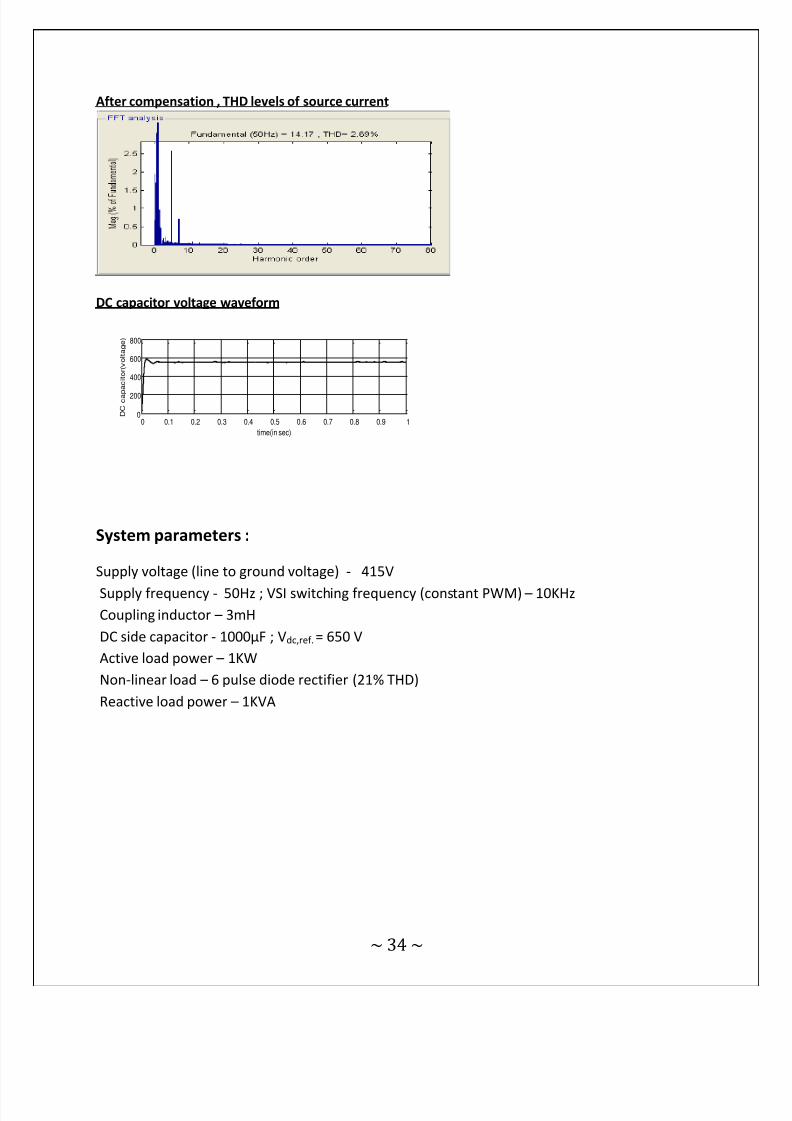
After compensation , THD levels of source current
DC capacitor voltage waveform
System parameters :
Supply voltage (line to ground voltage) - 415V
Supply frequency - 50Hz ; VSI switching frequency (constant PWM) – 10KHz
Coupling inductor – 3mH
DC side capacitor - 1000μF ; Vdc,ref. = 650 V
Active load power – 1KW
Non-linear load – 6 pulse diode rectifier (21% THD)
Reactive load power – 1KVA
0 0.1 0.2 0.3 0.4 0.5 0.6 0.7 0.8 0.9 10
200
400
600
800
time(in sec)
D C c
a p
a c i t o r ( v o l t a g e )

8/13/2019 Inverter,design inverter
http://slidepdf.com/reader/full/inverterdesign-inverter 42/51
~ 35 ~
CHAPTER#7
MULTILEVEL INVERTERS
7.1 INTRODUCTION
Numerous industrial applications have begun to require higher power apparatus in recent
years. Some medium voltage motor drives and utility applications require medium voltage and
megawatt power level. For a medium voltage grid, it is troublesome to connect only one power
semiconductor switch directly. As a result, a multilevel power converter structure has been
introduced as an alternative in high power and medium voltage situations. A multilevel
converter not only achieves high power ratings, but also enables the use of renewable energysources. Renewable energy sources such as photovoltaic, wind, and fuel cells can be easily
interfaced to a multilevel converter system for a high power application.
The concept of multilevel converters has been introduced since 1975. The term multilevel
began with the three-level converter. Subsequently, several multilevel converter topologies
have been developed. However, the elementary concept of a multilevel converter to achieve
higher power is to use a series of power semiconductor switches with several lower voltage dc
sources to perform the power conversion by synthesizing a staircase voltage waveform.
Capacitors, batteries, and renewable energy voltage sources can be used as the multiple dc
voltage sources. The commutation of the power switches aggregate these multiple dc sources
in order to achieve high voltage at the output; however, the rated voltage of the power
semiconductor switches depends only upon the rating of the dc voltage sources to which they
are connected.
A multilevel converter has several advantages over a conventional two-level converter that
uses high switching frequency pulse width modulation (PWM). The attractive features of a
multilevel converter can be briefly summarized as follows.
● Staircase waveform quality: Multilevel converters not only can generate the output
voltages with very low distortion, but also can reduce the dv/dt stresses; therefore
electromagnetic compatibility (EMC) problems can be reduced.
● Common-mode (CM) voltage: Multilevel converters produce smaller CM voltage;
therefore, the stress in the bearings of a motor connected to a multilevel motor drive can be
reduced. Furthermore, CM voltage can be eliminated by using advanced modulation strategiessuch as that proposed in .
● Input current: Multilevel converters can draw input current with low distortion.
● Switching frequency: Multilevel converters can operate at both fundamental
switching frequency and high switching frequency PWM. It should be noted that lower
switching frequency usually means lower switching loss and higher efficiency.
Unfortunately, multilevel converters do have some disadvantages. One particular disadvantage
is the greater number of power semiconductor switches needed. Although lower voltage rated
8/13/2019 Inverter,design inverter
http://slidepdf.com/reader/full/inverterdesign-inverter 43/51
~ 36 ~
switches can be utilized in a multilevel converter, each switch requires a related gate drive
circuit. This may cause the overall system to be more expensive and complex.
Plentiful multilevel converter topologies have been proposed during the last two decades.
Contemporary research has engaged novel converter topologies and unique modulation
schemes. Moreover, three different major multilevel converter structures have been reportedin the literature: cascaded H-bridges converter with separate dc sources, diode clamped
(neutral-clamped), and flying capacitors (capacitor clamped). Moreover, abundant modulation
techniques and control paradigms have been developed for multilevel converters such as
sinusoidal pulse width modulation (SPWM), selective harmonic elimination (SHE-PWM), space
vector modulation (SVM), and others. In addition, many multilevel converter applications focus
on industrial medium-voltage motor drives , utility interface for renewable energy systems ,
flexible AC transmission system (FACTS) , and traction drive systems .
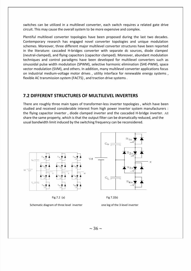
7.2 DIFFERENT STRUCTURES OF MULTILEVEL INVERTERS
There are roughly three main types of transformer-less inverter topologies , which have been
studied and received considerable interest from high power inverter system manufacturers :
the flying capacitor inverter , diode clamped inverter and the cascaded H-bridge inverter. All
share the same property, which is that the output filter can be dramatically reduced, and the
usual bandwidth limit induced by the switching frequency can be reconsidered.
Fig.7.2 (a) Fig 7.2(b)
Schematic diagram of three level inverter one leg of the 3-level inverter
8/13/2019 Inverter,design inverter
http://slidepdf.com/reader/full/inverterdesign-inverter 44/51
~ 37 ~
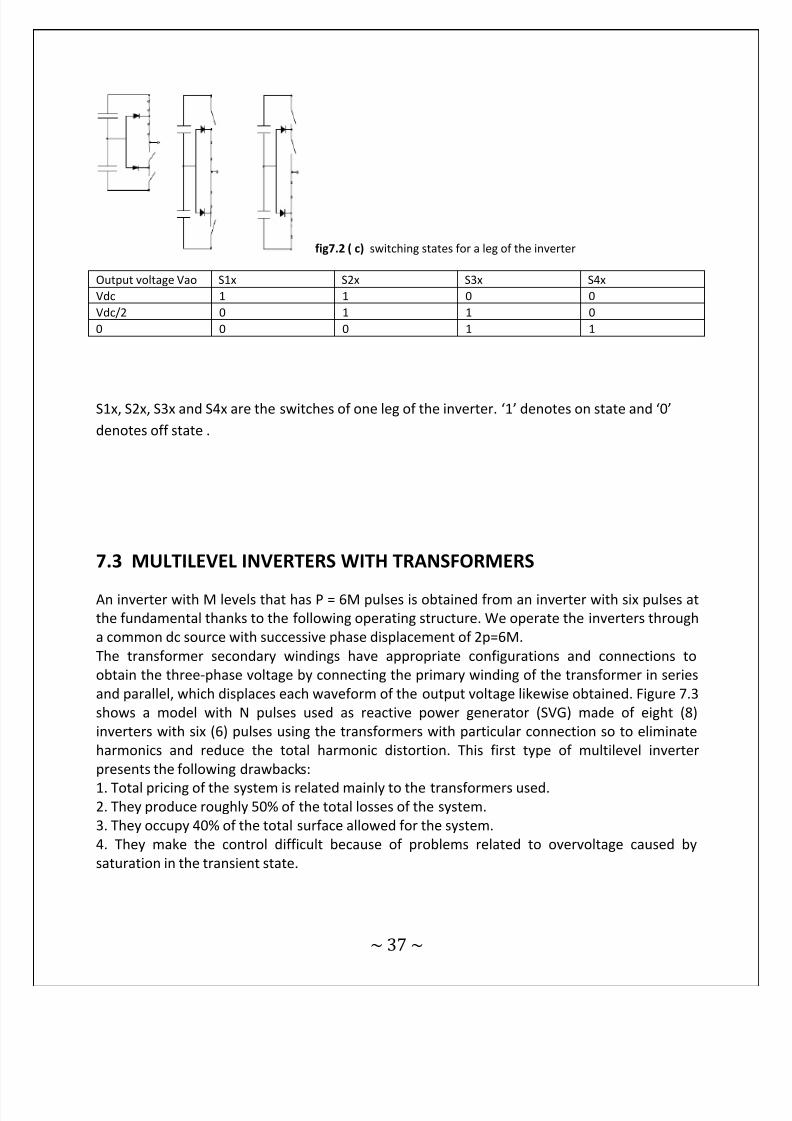
fig7.2 ( c) switching states for a leg of the inverter
Output voltage Vao S1x S2x S3x S4x
Vdc 1 1 0 0
Vdc/2 0 1 1 0
0 0 0 1 1
S1x, S2x, S3x and S4x are the switches of one leg of the inverter. ‘1’ denotes on state and ‘0’
denotes off state .
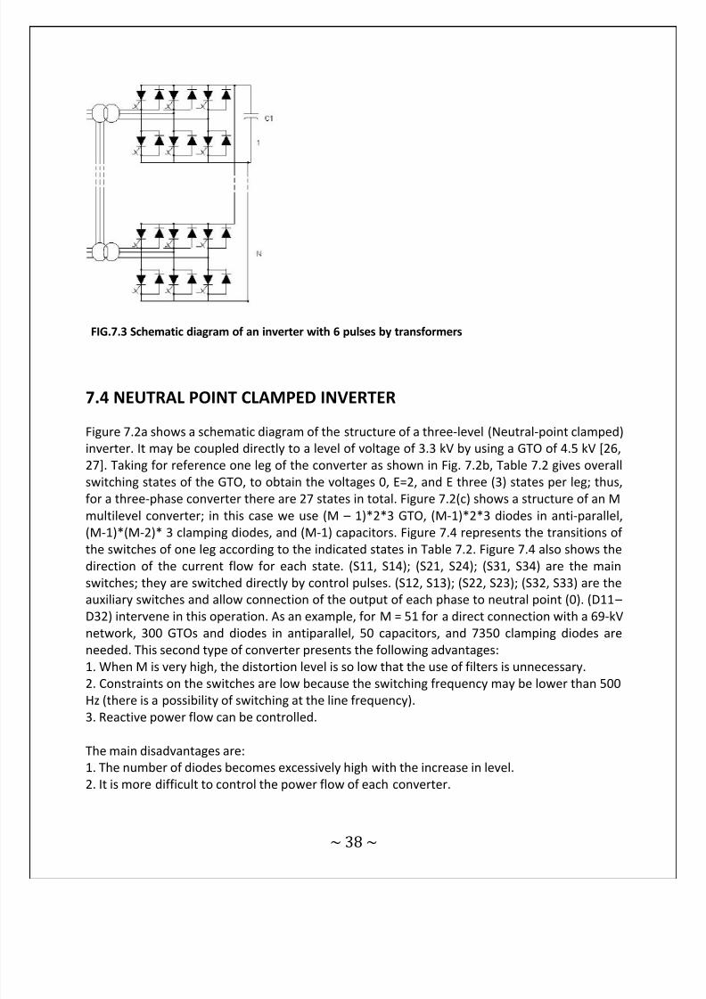
7.3 MULTILEVEL INVERTERS WITH TRANSFORMERS
An inverter with M levels that has P = 6M pulses is obtained from an inverter with six pulses at
the fundamental thanks to the following operating structure. We operate the inverters through
a common dc source with successive phase displacement of 2p=6M.
The transformer secondary windings have appropriate configurations and connections to
obtain the three-phase voltage by connecting the primary winding of the transformer in series
and parallel, which displaces each waveform of the output voltage likewise obtained. Figure 7.3
shows a model with N pulses used as reactive power generator (SVG) made of eight (8)
inverters with six (6) pulses using the transformers with particular connection so to eliminate
harmonics and reduce the total harmonic distortion. This first type of multilevel inverter
presents the following drawbacks:
1. Total pricing of the system is related mainly to the transformers used.2. They produce roughly 50% of the total losses of the system.
3. They occupy 40% of the total surface allowed for the system.
4. They make the control difficult because of problems related to overvoltage caused by
saturation in the transient state.
8/13/2019 Inverter,design inverter
http://slidepdf.com/reader/full/inverterdesign-inverter 45/51
~ 38 ~
FIG.7.3 Schematic diagram of an inverter with 6 pulses by transformers
7.4 NEUTRAL POINT CLAMPED INVERTER
Figure 7.2a shows a schematic diagram of the structure of a three-level (Neutral-point clamped)
inverter. It may be coupled directly to a level of voltage of 3.3 kV by using a GTO of 4.5 kV [26,
27]. Taking for reference one leg of the converter as shown in Fig. 7.2b, Table 7.2 gives overall
switching states of the GTO, to obtain the voltages 0, E=2, and E three (3) states per leg; thus,
for a three-phase converter there are 27 states in total. Figure 7.2(c) shows a structure of an M
multilevel converter; in this case we use (M – 1)*2*3 GTO, (M-1)*2*3 diodes in anti-parallel,
(M-1)*(M-2)* 3 clamping diodes, and (M-1) capacitors. Figure 7.4 represents the transitions of
the switches of one leg according to the indicated states in Table 7.2. Figure 7.4 also shows the
direction of the current flow for each state. (S11, S14); (S21, S24); (S31, S34) are the main
switches; they are switched directly by control pulses. (S12, S13); (S22, S23); (S32, S33) are the
auxiliary switches and allow connection of the output of each phase to neutral point (0). (D11 –
D32) intervene in this operation. As an example, for M = 51 for a direct connection with a 69-kV
network, 300 GTOs and diodes in antiparallel, 50 capacitors, and 7350 clamping diodes are
needed. This second type of converter presents the following advantages:
1. When M is very high, the distortion level is so low that the use of filters is unnecessary.
2. Constraints on the switches are low because the switching frequency may be lower than 500
Hz (there is a possibility of switching at the line frequency).3. Reactive power flow can be controlled.
The main disadvantages are:
1. The number of diodes becomes excessively high with the increase in level.
2. It is more difficult to control the power flow of each converter.
8/13/2019 Inverter,design inverter
http://slidepdf.com/reader/full/inverterdesign-inverter 46/51
~ 39 ~
Fig 7.4 Current flow
7.5 FLYING CAPACITOR INVERTER
fig.7.5
Figure 7.5 shows the structure of a flying-capacitor type converter. We notice that compared
to NPC-type converters a high number of auxiliary capacitors are needed, for M level
(M-1) main capacitors and (M-1)*(M-2)/2 auxiliary capacitors. The main advantages of this type
of converter are:
1. For a high M level, the use of a filter is unnecessary.
2. Control of active and reactive power flow is possible.
The drawbacks are:
1. The number of capacitors is very high.2. Control of the system becomes difficult with the increase of M.
8/13/2019 Inverter,design inverter
http://slidepdf.com/reader/full/inverterdesign-inverter 47/51
~ 40 ~
7.6 CASCADED TYPE MULTILEVEL INVERTER
This type of converter does not need any transformer clamping diodes, or flying capacitors;
each bridge converter generates three levels of voltages (E; 0, and ÿE). For a three-phase
configuration, the cascaded converters can be connected in star or delta. It has the
following advantages:1. It uses fewer components than the other types.
2. It has a simple control, since the converters present the same structure.
However, the main drawback is that it needs separate dc sources for the conversion of the
active power, which limits its use.
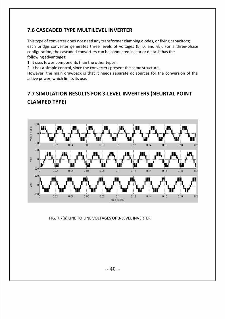
7.7 SIMULATION RESULTS FOR 3-LEVEL INVERTERS (NEURTAL POINT
CLAMPED TYPE)
FIG. 7.7(a) LINE TO LINE VOLTAGES OF 3-LEVEL INVERTER
8/13/2019 Inverter,design inverter
http://slidepdf.com/reader/full/inverterdesign-inverter 48/51
~ 41 ~
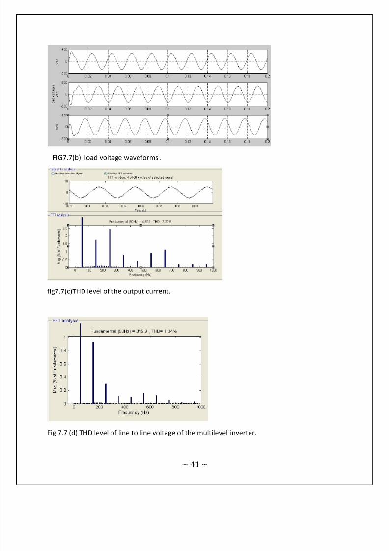
FIG7.7(b) load voltage waveforms .
fig7.7(c)THD level of the output current.
Fig 7.7 (d) THD level of line to line voltage of the multilevel inverter.

8/13/2019 Inverter,design inverter
http://slidepdf.com/reader/full/inverterdesign-inverter 49/51
~ 42 ~
7.8 System parameters
Dc voltage = 200V
Output Frequency = 50Hz
Active load power = 1 KW
Reactive load power = 700 VAR
CONCLUSION
The shunt active power filter for three phase three wire system was modeled in
MATLAB/SIMULINK and the simulations were carried out. The results achieved were
satisfactory and within the permissible limits in accordance to IEEE standards.
Similarly , the simulations for three level inverters was performed and the stepped
output voltages were obtained. Proper control strategies for switching of the multilevel
inverters were used .Care must be taken while implementing the switching strategies for it is
vital in the desired operation of the inverters .The harmonic distortions present in the load
current and voltage waveforms were observed and calculated through FFT analysis tool in
Matlab/simulink.
8/13/2019 Inverter,design inverter
http://slidepdf.com/reader/full/inverterdesign-inverter 50/51
~ 43 ~
REFERENCES
1. P.S.BHIMBRA , Power Electronics.
2. M.RASHID , Power Electronics
3. M.RASHID , Power Electronics Handbook (Academic Press Series In Engineering)
4. A. Tahri, A. Draou and M. Ermis, “A Comparative Study of PWM Control Techniques for Multilevel CascadedInverters,” Applied Power Electronics Laboratory, Department of Electrotechnics, University of Sciences andTechnology of Oran, BP 1505 El Mnaouar (31000 Oran),ALGERIA.
5. N.A. Rahim (Member IEEE), E.A.Mahrous, K.M.Sor(Senior Member IEEE), “Modeling And Simulation of Linear
Generator PWM Multilevel Inverter”, National Power and Energy Conference (PECon) 2003 Proceedings ,Malaysia.
6. Leon M Tolbert (Oak Ridge National Laboratory), Thomas.G.Habetler (Georgia Institute of Technology, School
of Electrical and Computer Engineering, Atlanta), “Novel Multilevel Inverter Carrier Based PWM Method”. 7. Surin Khomfoi and Leon M. Tolbert ,” Multilevel power converters “ , University of Tennessee . 8. G. Sinha, T.A.Lipo, “A Four Level Rectifier Inverter System for Drive Applications” ,IEEE IAS Annual Meeting
1996, pp 980-987 .
9. G.Carrara, D.Casini, S.Gardella, R.Salutari, “ Optimal PWM for the Control of Multilevel Voltage Source nverter”
, Fifth Annual European Conference on Power Electronics , volume 4 ,1993 ,pp255-259.10. S.Flora Viji Rose , Mr.B.V.Manikandan “ Simulation and Implementation of multilevel inverter based induction
motor drive”. 11. Samir Kouro, Jaime Rebolledo and J.Rodriguez, “Reduced Switching Frequency Modulation Algorithm for High
Power Multilevel Inverters,” IEEE Trans on Industrial Electronics, vol.54, no.5, Oct 2007.
12. A Nabae, I Takahashi and H Akagi. „A Neutral Point-clamped PWM Inverter‟. IEEE Transactions on IndApplication, vol IA-17, September/October 1981, pp 518-523.
13. J.K. Steinke. “Switching Frequency Optimal PWM Control of a Three-Level Inverter”. Proceedings of the 3rdEuropean Conference on Power Applications EPE‟89. Aachen, Germany.1989. pp. 1267-1272.
14. L. Tolbert, F.-Z. Peng, and T. Habetler, “Multilevel converters for large electric drives,” IEEE Trans. Ind.
Applicat., vol. 35, pp. 36 – 44, Jan./Feb. 1999.
15. G.Sundar and S.Ramareddy “Digital simulation of multilevel inverter based statcom “ , Journal of Theoretical and
Applied Information Technology ,2005.16. “The MATLAB compilers user‟s guide” in Mathworks hand book Math works 1994. 17. X. Li, R. Duke and S. Round. Development of a three phase three-level inverter for an electric vehicle.
Australasian Universities Power Engineering Conf .,Darwin, Australia, 1999, pp 247-251.
18. M. Lakshmi Swarupa, G. Tulasi Ram Das and P.V. Raj Gopal , Simulation and Analysis of SVPWM Based 2-
Level and 3-Level Inverters for Direct Torque of Induction Motor , International Journal of Electronic Engineering
Research ISSN 0975 - 6450 Volume 1 Number 3 (2009) pp. 169 – 184 .
19. N. S. Choi, J. G. Cho, G. H. Cho, “A General Circuit Topology of Multilevel Inverter,” IEEE Power ElectronicsSpecialists Conference, 1991, pp. 96-103.
20. J. Rodriguez, J. S. Lai and F. Z. Peng, “Multilevel Inverters: Survey of Topologies, Controls, and Applications,”IEEE Transactions on Industry Applications, vol. 49, no. 4, Aug. 2002, pp. 724-738.
21. Akagi,H.,et.al., "Instantaneous Reactive Power Compensation of switching Devices Without Energy Storage
Components" IEEE Trans.on Industry Applications, vol.20, no.3, May/JuneI984.
22. Akagi, H., "New Trends In Active Filters For Improving Power Quality," Proc.Of International conference
on Power Electronics, Drives and Energy Systems for Industrial Growth Vol. 1, pp. 417 - 425,January 1996
23. Akagi, H., "Active Harmonic Filters," Proc. Of IEEE. Vol. 93, No. 12 ,pp. 2128 - 2141, December 2005
Meo, S.~ Perfetto, A "Comparison of different control techniques for active filter applications, "
Proceedings of the Fourth IEEE International Caracas Conference on Devices, Circuits and Systems, P016-1 -
POI6-6,April 2002

8/13/2019 Inverter,design inverter
http://slidepdf.com/reader/full/inverterdesign-inverter 51/51
24. H. Akagi, E. H.Watanabe, and M. Aredes , Instantaneous Power Theory and Applications to Power
Conditioning . Hoboken, NJ:Wiley, 2007.
25. M. H. J. Bollen , Understanding Power Quality Problems: Voltage Sags and Interruptions, ser. IEEE Press
Power Eng. Piscataway, NJ: IEEE,2000.
26. S. Jain, P. Agarwal, & H.O.Gupta, "Design simulation and experimental investigations on a shunt active
power filter for harmonics and reactive power compensation", Electric Power Components and Systems, Vol.32, no. 7. July 2003pp 671-692
27. Ambrish Chandra, Bhim Singh, B.N. Singh and Kamal Al-Haddad, 2000. An Improved Control
Algorithm of Shunt Active Filter for Voltage Regulation, Harmonic Elimination, Power-factor Correction, and
Balancing of Nonlinear loads:IEEE Trans. Power Electronics, 15: 495-507
28. Akagi,H.,et.al., "Instantaneous Reactive Power Compensation of switching Devices Without Energy
Storage Components" IEEE Trans.on Industry Applications, vol.20, no.3, May/JuneI984 .
29. Akagi, H., "New Trends In Active Filters For Improving Power Quality," Proc.Of International
conference on Power Electronics, Drives and Energy Systems for Industrial Growth Vol. 1, pp. 417 -
425,January 1996.
30. Bhim Singh ,P.Jayaprakash , T.R.Somayajulu and D.P.Kothari “Reduced rating VSC with a zig-zag
transformer for current compensation in a three phase four wire distribution system. IEEE Trans. On PowerDelivery ,vol.24.,No.1,Jan2009