etching and thin film deposition -...
TRANSCRIPT

Etching and Thin Film DepositionProf. Steven Soper
1
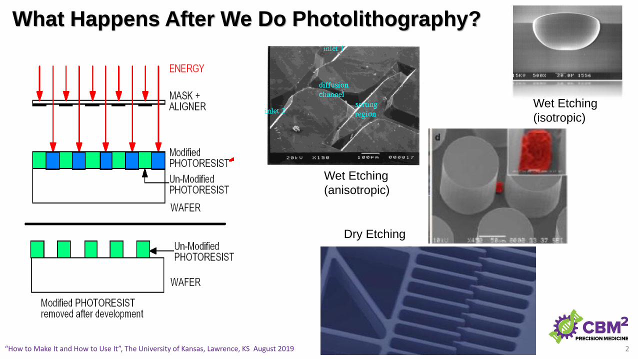
What Happens After We Do Photolithography?
Wet Etching
(anisotropic)
Wet Etching
(isotropic)
Dry Etching
“How to Make It and How to Use It”, The University of Kansas, Lawrence, KS August 2019 2

Etching
• Pattern transfer by chemical/physical removal of material from substrate where pattern is defined by a protective layer (photoresist, oxide, metal)
• Subtractive/Top-down process in which bulk material is removed to create smaller structures
Etching
Wet Etching Dry Etching
IsotropicAnisotropic
“How to Make It and How to Use It”, The University of Kansas, Lawrence, KS August 2019 3

Etching Metrics
Etch selectivity = Etch rate of material we want to remove (Vm)
Etch rate of masking material (Vr)
Etch Rate
• Etched depth per unit time
• If it’s too high, difficult to control
Uniformity – Percentage variation of etch across the wafer
Selectivity
• Ratio of etching rate between different materials, usually the higher the better
• Generally, chemical etching has higher selectivity, physical etching (sputtering, ion milling) has low
selectivity
“How to Make It and How to Use It”, The University of Kansas, Lawrence, KS August 20194

Wet Etching and Dry Etching
Wet etching
Dry etching
• Substrate is placed in chemical solution
and material is removed via chemical
reaction
• Benchtop process
• Substrate is placed in chamber
(typically gas in vacuum) .
• Etch species are accelerated towards
surface to remove material via chemical
and physical mechanisms
• More complex/expensive machinery
than wet etching
“How to Make It and How to Use It”, The University of Kansas, Lawrence, KS August 20195
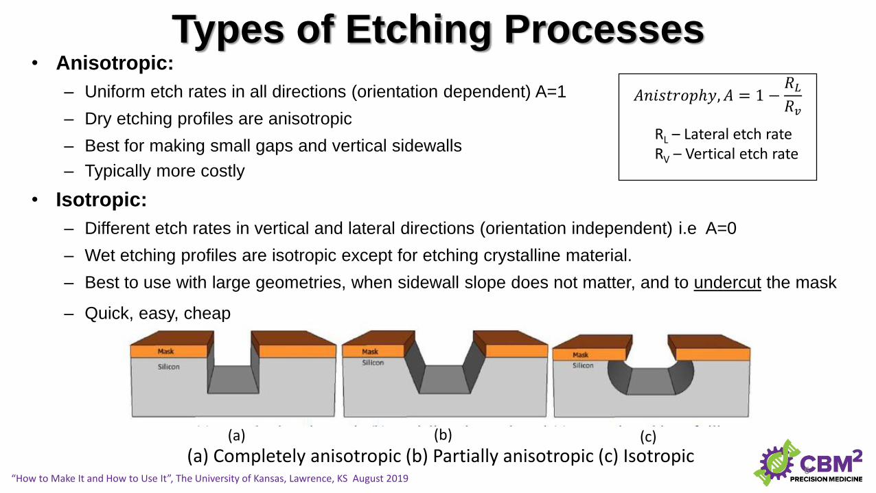
Types of Etching Processes• Anisotropic:
– Uniform etch rates in all directions (orientation dependent) A=1
– Dry etching profiles are anisotropic
– Best for making small gaps and vertical sidewalls
– Typically more costly
• Isotropic:
– Different etch rates in vertical and lateral directions (orientation independent) i.e A=0
– Wet etching profiles are isotropic except for etching crystalline material.
– Best to use with large geometries, when sidewall slope does not matter, and to undercut the mask
– Quick, easy, cheap
(a) (b) (c)(a) Completely anisotropic (b) Partially anisotropic (c) Isotropic
𝐴𝑛𝑖𝑠𝑡𝑟𝑜𝑝ℎ𝑦, 𝐴 = 1 −𝑅𝐿𝑅𝑣
RL – Lateral etch rateRV – Vertical etch rate
“How to Make It and How to Use It”, The University of Kansas, Lawrence, KS August 20196

Wet Etching in Microfluidics - SiliconWet Etching of Silicon can be isotropic or anisotropic (orientation dependent) depending on the etchant used
• Wet etching of Si recommended when dry process
is not available
• Performed with HNA: HNO3, HF, and acetic acid
(up to 50 µm/min)
• HNO3: oxidizes Si, HF: dissolves the generated
oxide layer, acetic acid is diluent
• Best masking material for HNA: Si3N4 or SiO2
Isotropic
Anisotropic etch in Si(100)
with KOH
Anisotropic
• Etch rate depends on crystalline orientation
• Typical solution is KOH > 20% at elevated temperature
(80-90 C)
• Relative etch rates: (110) > (100) > (111)
• Etch ratio of (100): (111) crystallographic planes is
~400:1
• Also common is 40% tetramethylammonium hydroxide
(TMAH) and ethylenediamine pyrocathecol (EDP)
• Can create an etch stop by doping with boron
Anisotropic etch in Si(110)
with KOH
“How to Make It and How to Use It”, The University of Kansas, Lawrence, KS August 20197

Wet Etching in Microfluidics - Glass
• Purely isotropic etch profiles
• Etched with solutions of hydrofluoric acid (HF)
(up to 8 µm/min)
• Glass is a mixture of oxides (CaO, MgO, Al2O3)
whose composition affects etching behavior
• HCl or H3PO4 can be added to remove
insoluble products and improve etch quality
(rate, morphology)
• Choice of masking layer is important to avoid
pinholes and delamination. Options include:
– Photoresist
– Amorphous Si
– Cr/Au
– Cr/photoresist
“How to Make It and How to Use It”, The University of Kansas, Lawrence, KS August 20198

Glass and Si WET Etchants for Microfluidics
Iliescu, Ciprian et al. “A Practical Guide for the Fabrication of Microfluidic Devices Using Glass and Silicon.”
Biomicrofluidics 6.1 (2012): 016505–016505–16. PMC. Web. 26 July 2016.
“How to Make It and How to Use It”, The University of Kansas, Lawrence, KS August 20199

Dry Etching Process• In dry etching, the etch reactants
come from a gas or vapor-phase
source and are typically ionized
– atoms or ions from the gas are
the reactive species that etch
the exposed film
• Solid surface is etched in
gas/vapor phase by physical
methods (sputtering, ion beam
milling) or chemical reaction
(using reactive gases or plasma)
or with combination of both
chemical and physical
bombardment (reactive ion
etching)“How to Make It and How to Use It”, The University of Kansas, Lawrence, KS August 2018 10

Types of Dry Etching
Type of Etching Excitation Energy Pressure
Plasma Etching 10’s to 100’s of Watts Medium
- isotropic, chemical, selective (>100 torr)
Reactive Ion Etching 100’s of Watts Low
- directional, physical & chemical, fairly selective (10-100 mtorr)
Sputter Etching 100’s to 1000’s of Watts Low
- directional, physical, low selectivity (~10 mtorr)
Dry etching spectrum
“How to Make It and How to Use It”, The University of Kansas, Lawrence, KS August 2019 11

Dry Etching
• Only role of plasma is to supply gaseous, reactive etchant
species
• Neutral chemical species responsible for most of reactive
etching (not ions)
• Ions rarely act as reactant species
• Volatile products removed by vacuum system
• Non-reactive species may decrease reaction rate by
blocking surface sites
Plasma etching
• Combines physical etching with chemical reactions
• Plasma etching with ion bombardment
• Ion-surface interactions promote dry etching by disrupting
unreactive substrate and causes damage (dangling bonds,
dislocations) resulting in substrate that is more reactive to
etchant
• Dry etchants for Si – CF4, SF6 & BCl2+Cl2 with etch rate of
~50nm/min.
Reactive Ion etching• Etching occurs as a result of a physical effect,
namely momentum transfer between energetic Ar+
ions and the substrate surface
• No chemical reaction involved
• Example : Sputtering and ion beam milling
• Plasma source can be dc or RF discharge
Physical dry etching
“How to Make It and How to Use It”, The University of Kansas, Lawrence, KS August 2019 12

Reactive Ion Etching (Dry Etching)
1. Wafer is grounded
2. Another electrode is connected to
the RF power source
3. Oscillating (RF) electric field
applied to ionize gas (~13 MHz)
4. Gas enters top of chamber and
exits bottom of chamber using
pump
5. Type of gas and pressure depend
on etch material and structure
demands (SF6 used for Si)
6. Gas ions (+) form in the chamber,
e- bombard the wafer, create (-)
surface
7. Voltage difference causes gas ions
to sputter material from wafer
“How to Make It and How to Use It”, The University of Kansas, Lawrence, KS August 2019 13

Step 1:
Etch
Step 3:
Repeat
Etch
Step 2:
Deposit
Polymer
• Etching occurs when fluorine radials react with the Si surface to form the
volatile reaction product SiF4 and is pumped away.
• A negative voltage bias on the wafer is used to control the flux of positive
ions from the plasma to the wafer surface.
• Etching is enhanced when SFx+ ions bombard the Si surface, making it
more reactive.
• A fluorocarbon (nCF2) passivation layer is deposited to prevent etching
of side-walls.
• By quickly cycling between passivation and etching steps, very high aspect
ratio features (etch depth/feature width) can be created.
• An inherent characteristic of the Bosch process due to alternating
passivation/etch steps is side-wall scalloping.
Dry etching - Deep Reactive Ion Etching (DRIE)• Dry etching technique used for creating high aspect ratio structures in Si,
SiO2, quartz, and some metals
• High density plasma enables etch rates much higher than standard RIE
• High aspect ratio features are achieved using the Bosch process (cryogenic DRIE also capable of high aspect ratios)
• Preferred method of etching Si compared to wet etching
Bosch Process
High aspect ratio features in Si
Characteristic scallops from Bosch process Microfluidic mold etched in Si by DRIE
“How to Make It and How to Use It”, The University of Kansas, Lawrence, KS August 2019 14

Wet vs. Dry EtchingWet Etching Dry Etching
High selectivity (up to 100:1) Relatively low selectivity (1:1 but much
higher with metals)
High etch rate (many microns/minute) Relatively slow etch rates (< 1um/min but
can be much higher)
Low cost Expensive
Batch system with high throughput High aspect ratio features due to high
anisotropy (> 20:1)
Limited resolution (inadequate for <1 um) Capable of defining submicron features
Generally isotropic (anisotropic possible
for single crystalline materials)
Vertical profiles can be produced in
crystalline, polycrystalline, and
amorphous materials
Generates a lot of waste Clean process
Hard to control (not reproducible) Potential heat/radiation damage
“How to Make It and How to Use It”, The University of Kansas, Lawrence, KS August 2019 15

Wet vs. Dry Etching - Example
Wet etched Cr Dry etched (RIE) Cr
“How to Make It and How to Use It”, The University of Kansas, Lawrence, KS August 2019 16

Putting Down Thin Films
1. Etching processes:
Spin photoresist (PR) PhotolithographyEtch using PR
as maskRemove PR
2. Lift off processes
Evaporate metalSpin (PR)Lift Off excess
metal with PRPhotolithography
patterning of difficult to etch metals (Pt)
preparation of optical masks, patterning metals, oxides, etc…,
patterning microfluidic channels in glass, silicon
17“How to Make It and How to Use It”, The University of Kansas, Lawrence, KS August 2019

Atomic Layer Deposition (ALD)
• Precise control of layer thickness
• Films are highly conformal – uniform coating on films,
particles, and porous samples
• Stoichiometric control
• Low temperature process (as low as RT)
• Excellent adhesion due to chemical bonds at first layer
Advantages
But, very slow! Many hours for 10’s of nms
LixTiOy deposited by ALD in 300:1 AAO nanotemplates
Al2O3 – ZrO2 nanolaminates
18“How to Make It and How to Use It”, The University of Kansas, Lawrence, KS August 2019

Atomic Layer Deposition
19“How to Make It and How to Use It”, The University of Kansas, Lawrence, KS August 2019

Physical Vapor Deposition (PVD)• PVD: Deposition technique in which some form of energy is used to transfer material from a
target to the substrate, where it condenses a) Thermal evaporation
• Heated filament used to boil off material
• Depositing alloys is difficult
• Poor adhesion
• Poor step coverage
• Not possible for refractory metals (limited choice of materials)
d) Sputter deposition
• Plasma creates ions that are accelerated toward target. Momentum
transfer from ions to target causes target material to be ejected toward
surface (sputtering), where it condenses
• High purity films over large area are possible
• Just about any material can be sputtered – including compounds, but
used mainly for metal deposition
• Better step coverage than evaporated films, but not always as smooth
• Deposition rate: 10’s nm/min
Thermal evaporation E-beam evaporation
Pulsed laser deposition Sputter deposition
b) Electron beam evaporation
• High intensity electron beam focused on target material causes evaporation
• Deposition rates (10’s nm/min)
• Wider choice of materials
• Higher purity films
• Can cause x-ray and/or ion damage to substrate
c) Pulsed laser deposition
• Like e-beam evaporation, but laser is used instead for removing
target material
• Wide choice of target materials
• High purity
• Slow dep. rates
20“How to Make It and How to Use It”, The University of Kansas, Lawrence, KS August 2019

Sputter Deposition
• Voltage is applied across a rarified gas
• Breakdown of the gas forms a plasma
• Positive ions from plasma strike the negative electrode (cathode and target)
• Energy from the ions is transferred to the target atoms
• Some target atoms escape from target surface (they are sputtered)
• The sputtered atoms condense on the substrate
• Deposition of compounds (oxides, nitrides) possible with introduction of
reactive gases Sputtering targets with plasma ignited
Various sputtering target geometries
21“How to Make It and How to Use It”, The University of Kansas, Lawrence, KS August 2019

Sputter Deposition – Film profiles
• Just about any material can be sputtered (including compounds and refractory metals)
• Metal oxides and nitrides can be deposited via reactive sputtering
• Reactive sputtering: metal sputtering in the presence of a reactive gas
• Better step coverage than evaporated films, but not always as smooth
• Deposition rate: 10’s nm/min
• Not good for shadow masks due to angular distribution of ion trajectory
Typical deposition profile of film sputtering into a trenchPatterning sputtered films using a shadow mask
22“How to Make It and How to Use It”, The University of Kansas, Lawrence, KS August 2018

Electron Beam Evaporation
• Electrons are generated by electron gun (cathode)
• Emitted electrons are accelerated towards crucible
(anode) by high voltage potential
• Localized heating of target material (evaporation)
• Deposition with reactive species to create metal
oxide/nitrides is possible
• High purity films compared to PVD
• Can be used with shadow masks
Schematic of e-beam evaporation system
Electron gun for e-beam evaporation system
23“How to Make It and How to Use It”, The University of Kansas, Lawrence, KS August 2019
Electron beam
focused on
crucible

SEMs of Thermally and E-beam Evaporated Al Films
24“How to Make It and How to Use It”, The University of Kansas, Lawrence, KS August 2019