eterna integration guide - analog.com · the eterna is most sensitive to supply noise in the 100 to...
TRANSCRIPT

Dust Networks
Eterna Integration Guide

2 ETERNA INTEGRATION GUIDE
Table of Contents Design Process ......................................................................................................... 4
About This Guide ...................................................................................................... 5
Audience ................................................................................................................. 5
Related Documents .................................................................................................. 5
Conventions and Terminology.................................................................................... 5
Revision History ....................................................................................................... 5
General Design Guidelines........................................................................................ 7
Schematic Design ..................................................................................................... 7
Crystal Selection ...................................................................................................... 9
System Configuration ..............................................................................................10
PCB Layout .............................................................................................................10
Eterna QFN 72 Lead Recommended Land Pattern (QFN package QH072AF2A) ...........12
Stencil Design for Ground Paddle (QFN package QH072AF2A) ..................................14
EMI Considerations ..................................................................................................14
Antenna ESD Considerations ....................................................................................16
Supply Design .........................................................................................................16
Voltage Supervision and Reset .................................................................................16
Design for Manufacture ............................................................................................17
External Memory Support ....................................................................................... 18
Schematic Design ....................................................................................................18
Device Configuration ...............................................................................................21
List of Figures Figure 1 Eterna Example Schematic .......................................................................... 7
Figure 2 Sample 20 MHz Crystal Routing ................................................................. 11
Figure 3 Triple 20 MHz crystal footprint with solder mask over pad ............................ 12
Figure 4 72 Lead QFN Land Pattern (QFN package QH072AF2A) ................................ 13
Figure 5 Ground Paddle Stencil ............................................................................... 14
Figure 6 Eterna Extended Memory Example Schematic (page 1 of 2) ......................... 19
Figure 7 Eterna Extended Memory Example Schematic (page 2 of 2) ......................... 20

ETERNA INTEGRATION GUIDE 3
List of Tables Table 1 Sample BOM .................................................................................................. 8
Table 2 20 MHz Crystals ............................................................................................. 9
Table 3 32 kHz Crystals............................................................................................ 10
Table 4 Recommended Land Pattern Dimensions ........................................................ 13
Table 5 External Memory Reference Bill of Materials ................................................... 20

4 ETERNA INTEGRATION GUIDE
Design Process
The design process when working with the LTC5800 based products is very similar to the design process when working with an embedded microprocessor with some significant and important differences covered in this section. The integration guide focuses on the steps to design and manufacture LTC5800 based PCAs. Design of a system solution should be completed with an understanding of the integration guide and the network as described in either the SmartMesh IP User Guide or the SmartMesh WirelessHART User Guide. In addition, if developing software on the LTC5800-IPM, the software development process and API definitions are provided on www.dustcloud.org.
After defining how the product(s) should operate in network and how the design will be partitioned between hardware and software the design will typically take the following steps:
1) Review the example schematic provided in this document to gain familiarity with the required additional PCA components.
2) For customers developing software on the LTC5800-IPM, use the Fuse Table application as described in the Eterna Board Specific Configuration Guide to assign functions, such as SPI, I2C and GPIO to IOs.
3) Follow this document to complete the schematic design and layout.
4) Use the Fuse Table application as described in the Eterna Board Specific Configuration Guide to create a fuse table for the design.
5) Use the Eterna Serial Programmer to load all of the required images onto the LTC5800, the Fuse Table, Loader, Partition table and Image.
6) As described in the Eterna Serial Programmer Guide, characterize the 20MHz crystal in the design. Update the Fuse Table with the new 20 “MHz load trim (ox13)” value.
7) Develop and debug the design. Use the commands described in the ETERNA RF Certification Users Guide, to perform out of network RF tests as needed.
8) Have the design pre-screened for RF certification on each revision of the PCB.
9) Develop production tests. The Eterna Serial Programmer is intended for loading flash images in production. The LTC5800 BDSL file provides an efficient method to test PCB interconnect.
10) The ETERNA RF Certification Users Guide provides a complete set of the LTC5800 specific information and commands required to certify an LTC5800 based PCB worldwide. Certification can be a lengthy process requiring significant supporting documentation from the manufacturer. Customers are recommended to work with a certification agency familiar with the regulations in the geography/geographies the design will be certified. The ETERNA2 RF Certification Users Guide and the ETERNA2 Certification Package can be used as an example for the radio specific documentation required for several geographies, including: Canada, United States of America, the European Economic Union, Japan, Taiwan, Korea, Australia, New Zealand and India.

ETERNA INTEGRATION GUIDE 5
About This Guide
This document provides the design guidelines essential for incorporating a LTC5800-based design. The document covers design, layout, EMI, some device configuration and manufacturing considerations.
Audience
This document is intended for system developers, hardware designers, and layout engineers.
Related Documents
The following related documents are available:
Eterna Integration Guide (this guide)
600- 0180 MASTER_SCHEMATIC_ETERNA_MOTE_EUPHRATES.pdf
600- 0180 MASTER_SCHEMATIC_ETERNA_MOTE_EUPHRATES.dsn
600- 0180 ETERNA_MOTE_EUPHRATES.pcb
Eterna Board Specific Configuration Guide
Eterna Serial Programmer Guide
605-0211 MASTER_SCHEMATIC_ETERNA_MEMORY_REFERENCE_ELWHA.pdf
605-0211 MASTER_SCHEMATIC_ETERNA_MEMORY_REFERENCE_ELWHA.dsn
Conventions and Terminology
This guide uses the following text conventions:
Computer type indicates information that you enter, such as a URL.
Bold type indicates buttons, fields, and menu commands.
Italic type is used to introduce a new term.
Note: Notes provide more detailed information about concepts.
Caution: Cautions advise about actions that might result in loss of data.
Warning: Warnings advise about actions that might cause physical harm to the hardware or your person.
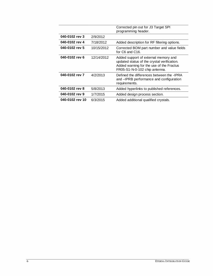
Revision History Revision Date Description
040-0102 rev 1 5/6/2011 Initial Release
040-0102 rev 2 11/8/2011 Added QH072F1A Land Pattern Recommendations. Added Solder mask over pad recommendations for the 20 MHz xtal. Added recommendations for QH072F1A paddle solder stencil design.
6 ETERNA INTEGRATION GUIDE
Corrected pin out for J3 Target SPI programming header.
040-0102 rev 3 2/9/2012
040-0102 rev 4 7/18/2012 Added description for RF filtering options.
040-0102 rev 5 10/15/2012 Corrected BOM part number and value fields for C6 and C16.
040-0102 rev 6 12/14/2012 Added support of external memory and updated status of the crystal verification. Added warning for the use of the Fractus FR05-S1-N-0-102 chip antenna.
040-0102 rev 7 4/2/2013 Defined the differences between the -IPRA and –IPRB performance and configuration requirements.
040-0102 rev 8 5/8/2013 Added hyperlinks to published references.
040-0102 rev 9 1/7/2015 Added design process section.
040-0102 rev 10 6/3/2015 Added additional qualified crystals.
ETERNA INTEGRATION GUIDE 7
General Design Guidelines
Schematic Design
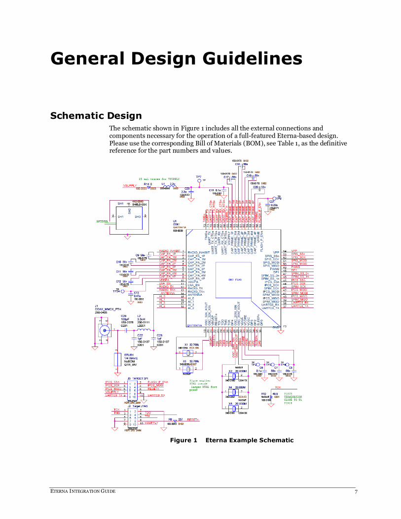
The schematic shown in Figure 1 includes all the external connections and components necessary for the operation of a full-featured Eterna-based design. Please use the corresponding Bill of Materials (BOM), see Table 1, as the definitive reference for the part numbers and values.
Figure 1 Eterna Example Schematic

8 ETERNA INTEGRATION GUIDE
The design includes power supply filtering via C23, C16, R14, and L1. The capacitor, C16, must always be included and must be a ceramic type (X7R is recommended for solutions requiring a wide temperature range and X5R otherwise) in order to support the high frequency transient currents on the Eterna power supply. Note that R14 is present to de-Q L1. The Eterna is most sensitive to supply noise in the 100 to 2000 kHz band. The included filter will reduce noise in the most sensitive band by roughly an order of magnitude and is not required for all supply designs. However, it is essential to meet the Eterna’s power supply requirements for maximum noise considering both steady state operation and transient response.
An RF shield is typically required to obtain modular certification. However, it provides minimal benefit in typical environments in providing isolation from RF and magnetic fields. The RF shield matching the reference designs is available from DigiKey and LTC eCOM (part number DUST-SHLD01).
Capacitors C6 through C13 and C16 through C21 are used for on chip regulation of power supplies and should be placed as close as possible to their corresponding package leads. These capacitors must be X7R. L2, C22 and C28 are placeholders for a Pi matching network, where these components may be either capacitors or inductors as dictated by the match required. The values in the BOM represent the current matching required for a 50-Ohm load. Warning: C29, acting as DC blocking capacitor is required to connect Eterna’s ANTENNA pin to a DC grounded antenna or a DC grounded ¼ wave stub.
STUB1, connected to the RF path near the antenna connector is a ¼ wave, at 2.44 GHz, microstrip terminated to ground. The ¼ wave stub provides a notch filter at the 2nd harmonic, enabling Eterna to easily meet world wide certification requirements while only having slight impact on radio performance. The use of the ¼ wave stub significantly improves ESD performance while having near zero cost and is the preferred approach to lowering the 2nd Harmonic emissions. It should be expected to trim the layout of a ¼ wave stub in layout to center the notch of the ¼ wave stub. Using the Pi matching network will have a higher production cost and lower ESD performance; however, the Pi matching network provides customers with the ability to tune the filter without requiring a spin of the PCB. Warning: The Fractus FR05-S1-N-0-102 chip antenna has demonstrated high gain lobes when used in combination with a ¼ wave stub which may prevent a design from passing radio certification. When using the Fractus FR05-S1-N-0-102, ESD the Pi-filter comprising L2, C22 andC28 should be used. When using a ¼ wave stub designs need not incorporate L2, C22 and C28; however, conservative practice would be to include the layout supporting those components and loading L2 with a 100 pF capacitor (this allows for matching and additional filtering should it be necessary). Should layout considerations prevent the use of a ¼ wave stub, a low pass Pi-filter comprised of L2, C22 and C28 may be used. Board stack up should be chosen such that the trace width of the RF path, a 50 ohm impedance, is equal to or near the pad side for the 0201 components.
Table 1 Sample BOM
Reference Value Vendor Vendor P/N
R14 0 Yageo RC0603JR-070RL
R8 237 Vishay CRCW0402237RFKED
C7, C8, C9, C10, C11, C12, C17, C18, C19, C20
56 nF Kemet C0402C563K9RACTU
C21 220 nF Taiyo Yuden
JMK105B7224KV-F
C22*, C28* 1 pF Murata GRM610C0G010B25K500

ETERNA INTEGRATION GUIDE 9
Reference Value Vendor Vendor P/N
C29 100 pF Murata GRM0335C1E101JD01D
C6,C16 100 nF Murata GRM155R71C104KA88D
C23 2.2 µF Murata GRM188R71A225KE15D
C13 470 nF TDK C1005X5R0J474K
L1 2.2 µH Murata LQM18FN2R2M00D
L2* 3.3 nH 0201 or 2.7 nH 0402
Coilcraft Coilcraft
0201DS-3N3XJL
0402CS-2N7XJL
J1 JST AYU1-1P-02676-120
X1 32.768 kHz ECS Inc. ECS-.327-12.5-17X-TR
X2 20.000 MHz ECS Inc. ECS-200-CDX-0914
J2, J3 5x2 header Molex 87831-1020
SH1 Fotofab DUST-SHLD01
Note: * - these components are not needed if a ¼ stub is implemented.
Crystal Selection
The 20 MHz source (either X2, X4 or X5 on the schematic) is required for radio operation. The 32 kHz source, either X1 or X3 on the schematic, is required for long term precise timing. For mesh network applications, selection of crystal sources is significant as Eterna mesh networks depend on maintaining timing more precise than provided by the crystal accuracy itself. While alternate sources for the 20 MHz and 32 kHz crystals may operate without issue, it is strongly recommended that designs incorporate crystals from Table 2 and Table 3 below, such that the designs will benefit from the verification performed against those crystals. Commonly available crystals have failed Dust Networks qualification suite. Network performance for unverified crystals can not be guaranteed.
Selection of a particular 20MHz crystal for use in a design should be matched by selecting the same crystal in the Board Support Parameter “20 MHz xtal Part Number” in the Fuse Table application. The ECS-200-CDX-0998 and the Kyocera CX3225SB20000F0FZZC1 may be used interchangeably with a single Fuse Table image.
Table 2 20 MHz Crystals
Vendor Part Number Form Factor
ECS ECS-200-CDX-0998* 3.2x2.5x0.8mm, SMD
KYOCERA CX3225SB20000F0FZZC1* 3.2x2.5x0.9mm, SMD
ECS ECS-200-CDX-0778 2.5x2.0x0.55mm, SMD
ECS ECS-200-CDX-0914 7.6x4.1x2.3mm, SMD
* These crystals are both footprint compatible and will work with a single Fuse Table configuration. As a result one can be second sourced for the other.

10 ETERNA INTEGRATION GUIDE
Table 3 32 kHz Crystals
Vendor Part Number Form Factor
ECS ECS-.327-12.5-17X 8.7x3.7x2.5mm, SMD
Abracon ABS07-32.768KHZ-4-T 3.2x1.5x0.9mm, SMD
ECS ECS-.327-12.5-34B-TR 3.2x1.5x0.9mm, SMD
NDK NX3215SA-32.768K-STD-MUA-8 3.2x1.5x0.9mm, SMD
System Configuration
Eterna supports hardware and software configuration of devices via two tables stored in the first page of Eterna’s flash. These configurations are set by creating a 2kB image via the Eterna Board Specific Configuration application described in the Eterna Board Specific Configuration Guide and written to Eterna’s flash via the Eterna Serial Programmer described in the Eterna Serial Programmer Guide.
Eterna includes a hardware engine for configuring the device immediately on exit from power-on reset and is the preferred method for configuring the multifunction IO. Configuration controls include the mapping of pins to functions, setting drive strength, IO direction, GPIO output value, pull enable, pull direction, and input enable. In addition the Eterna’s Hardware lock key, a user defined key that locks all external access (including debug access) to flash and RAM memory, can be set via the Eterna Board Specific Configuration application. The Eterna Board Specific Configuration application inherently provides an expedient method to map out the functions assigned to Eterna’s multifunction IO, greatly reducing the need to manually cross reference multiple tables in the product’s data sheet.
PCB Layout
Eterna-based designs should adhere to the following layout-sensitive guidelines:
1. The trace from the ANTENNA pin to the antenna connector should be 50-Ohm characteristic impedance. Note that the drawn trace width will be a function of the dielectric constant, height of the dielectric and the thickness of the plating. For example, for an 8-mil FR4 substrate with 0.5 oz copper plating, the width for a 50-Ohm trace is 14.5 mils. Keep all other active signals as far as possible from this trace and at least five times the dielectric height to the RF ground plane. No signals should be routed between this trace and its respective ground plane.
2. The ground return for the ANTENNA pin is through the QFN paddle. The layout should ensure that at least a 25 mils wide ground (and preferably as wide as practically manageable) continues in a straight line through to the points where the paddle is via stitched to ground.
3. Capacitors C6 through C13 and C16 through C21 should be placed no further than 250 mils from their respective leads. All power supply traces for VSUPPLY, VPRIME, VDDPA, VOSC, VCORE and VDDA should be a minimum of 25 mils wide.
4. Noise from other digital signals can couple onto the 20 MHz crystal reference and impair the radio performance. Traces from the 20 MHz crystal should be routed on the same outside layer as the Eterna QFN, with no overlap from any

ETERNA INTEGRATION GUIDE 11
other signal, as shown in Figure 2. The adjacent layer on the PCB shall provide a ground plane, isolating the crystal traces from other traces on the PCB. The crystal leads and the corresponding traces should be surrounded by a co-planer ground trace to reduce coupling onto the crystal pads and traces. If a shield is present in the design the signals should rout through an opening in the exposed metal trace described in the RF shield section below.
Figure 2 Sample 20 MHz Crystal Routing
5. Noise from other digital signals can couple onto the 32-kHz crystal reference creating timing jitter for the low frequency clock. Traces from the 32 kHz crystal should be routed on the same outside layer as the Eterna QFN, with no overlap from any other signal. The adjacent layer on the PCB shall provide a ground plane, isolating the crystal traces from other traces on the PCB. If a shield is present in the design the signals should rout through an opening in the exposed metal trace described in the RF shield section below.
6. In applications where EMI necessitates the inclusion of an RF shield, a thick outside layer exposed metal trace, tapped to ground approximately every 100 to 250 mils, should encircle (save the path for the antenna and crystal signals) the device. Determination for the size of the shield should account for the routing challenges placed due to the limited area to create vias from the outside layer with the QFN to other layers for routing. The shield will create a bounding box on the outside with the QFN paddle will create an internal bounding box. Also, consider the number of connections that should be as short as possible for the required power supply components that should be placed near the QFN leads.

12 ETERNA INTEGRATION GUIDE
7. The recommended land pattern for the smaller footprint crystals, 3.2mm x 1.5mm, includes pads that are much wider than the crystal leads. Creating a dual footprint for both the large and smaller form factor 20 MHz crystals further enlarges the pad size. The large pad size can result in crystals drifting from their placement during the reflow process. Reducing the pad size reduces a design ’s robustness to vibration, which could be an important factor given the mass of either the larger 20 MHz crystals. With the purpose of reducing the drift of the crystal during the reflow process, it is recommended to include additional solder mask over the pad as show in red in Figure 3.
Figure 3 Triple 20 MHz crystal footprint with solder mask over pad
An example layout corresponding to the provided example schematic, can be found in 600- 0180 ETERNA_MOTE_EUPHRATES.pcb, a PADs formatted PCB file and it’s corresponding gerber files.
Eterna QFN 72 Lead Recommended Land Pattern (QFN package QH072AF2A)
Two common practices for defining land patterns are Non Solder Mask Defined, NSMD, and Solder Mask Defined, SMD. Given the lead pitch of the QH072AF2A package and that tolerances for metal etch are commonly more precise than solder mask deposition, the use of NSMD land patterns is recommended and documented here. The solder mask opening should provide sufficient margin for registration tolerance to avoid solder mask infringing on the pad, typically 60 to 75 um from the edge of the pad and the solder mask. Note that the lead length for the corner leads are shorter than the non-corner leads.
While Eterna does not require the ground paddle to dissipate significant thermal energy, the paddle provides the RF return path and should both be low inductance and provide a path near the ANTENNA pin for a return path. A pattern of 3 x 3 vias separated over a 4.5 mm x 4.5 mm square is recommended. Vias should be plugged with epoxy or tented to avoid solder wicking into the plated through holes, potentially resulting in low package standoff height or secondary reflow on the reverse side of the PCB.

ETERNA INTEGRATION GUIDE 13
Land Pattern and Via placement dimensions are provided in Table 4 and illustrated in Figure 4.
Table 4 Recommended Land Pattern Dimensions
Symbol Description Dimension (mm)
Min Typ Max
A Lead land width 0.25 - 0.29
B Lead land length 0.85 - -
Corner Lead land length 0.75 - -
C Lead land pad inside dimension 8.70 8.80
Corner lead land pad inside dimension
8.90 9.00
D Lead land pad outside dimension 10.50 - -
E Ground paddle land width 6.15 - -
F Center first lead to package edge - 0.75 -
G Ground via spacing center to center
- 4.5 -
E
E
D
DC
F
F
A
B
G
G
Figure 4 72 Lead QFN Land Pattern (QFN package QH072AF2A)

14 ETERNA INTEGRATION GUIDE
Stencil Design for Ground Paddle (QFN package QH072AF2A)
As the Eterna (QH072AF2A QFN) includes a 6 x 6 mm ground paddle, appropriate care should be taken in designing the solder stencil. Large apertures in the solder stencil can lead to:
1) inadequate solder paste due to “scooping”
2) splatter and solder balling as a result of outgassing
3) increased standoff mismatch between leads on a QFN package
4) solder bridging
It is recommended to use smaller openings separated by at least 0.2 mm, with a coverage of between 50 and 80%. An example of such a stencil with 1.6 mm squares separated by 0.3 mm, providing 64% coverage is shown in Figure 5.
Figure 5 Ground Paddle Stencil
EMI Considerations
Like all radio devices, Eterna can be sensitive to EMI. In cases where the deployment environment is known to have very low EMI, both in and out of band, the RF shield may not be necessary. It should be noted; however, that for modular radio certifications, regulatory bodies regularly require an RF shield. The following considerations should be taken into account when selecting an RF shield for an Eterna based design:
1. The RF shield should provide at least 0.5 mm (20 mils) clearance around the Eterna package in the X and Y dimensions.
2. The RF shield should provide 1 mm (40 mils) of clearance above the top of the PCB to the inside of the shield.
3. The RF shield should have a minimum of three asymmetric through hole pins. In vibration intensive use cases, a minimum of four through hole pins should be used and the RF shield should mate those pins to plated mounting holes and the majority of the shield perimeter should be soldered to the PCB.
4. Ideally, the RF shield should allow for the smallest opening, but still greater than 5 times the dielectric thickness between the antenna trace and the ground plane from edge/top of the antenna trace to the nearest edge of the shield, for

ETERNA INTEGRATION GUIDE 15
the antenna signal to exit on the top layer of the PCB. This needs to be traded-off against the cost of manufacture, including the ability to clean the PCB underneath the shield.
5. In environments with high AC and DC magnetic fields, the use of a mu-metal shield is recommended. Further, RF shield thickness is application dependent. Consult your Linear FAE for support.
16 ETERNA INTEGRATION GUIDE
Antenna ESD Considerations
The antenna pin is a particularly sensitive node for electro-static discharge (ESD) since it must detect small, high-frequency signals. ESD damage to the Eterna may result in decreased receive or transmit performance, or other system failure. Many applications for the Eterna have an exposed antenna that provides an entry point for ESD events. Proper consideration of antenna design as well as antenna protection can substantially improve ESD robustness in harsh environments.
A radome (protective covering) made of highly resistive material may be used to prevent direct contact with the antenna and/or dissipate charge. To avoid ESD events caused by triboelectric charging generated by wind passing over the antenna in dry climates, the radome design should consider bulk and surface resistivity as well as the size of the gap between the antenna metal and the interior of the radome.
In general, DC-grounded antennas (the antenna and ground have a DC short) provide superior protection to ESD events. DC-grounded antennas are highly recommended in harsh environments. Additionally, a DC path-to-earth ground should be provided whenever possible to help bleed off accumulated charge from the antenna as well as leak charge from the radome.
While these general guidelines should improve robustness to ESD events, individual implementations may have unique factors that complicate ESD protection. Upon request, your Linear FAE can provide contact information for an external consultant able to perform a review for ESD and other system considerations.
Supply Design
Due to the heavy duty cycling, the Eterna’s current consumption can change substantially over a short period. This does not represent an issue for systems with supplies having low source impedance (less than 5 Ohms). Regulated supplies, however, may have difficulty in the sudden changes in current consumption (more than an order of magnitude in less than 1 µs), resulting in transient voltages on the supply co-incident with the higher current consumption of the radio operation. To ensure proper operation of the radio, a supply should be able to ramp from 250 µA to 10 mA in less than 1 µs without generating a transient greater than 200 mV. For systems with regulated supplies, consultation with your Linear Technology FAE is strongly recommended.
The Eterna can be configured to support current limited supplies. Contact your Linear FAE for details.
Voltage Supervision and Reset
The Eterna includes a power-on reset to safely set its own state during power up, and includes a brown-out circuit that immediately halts flash erase cycles and interrupts flash write cycles at the next 32-bit boundary, generating an interrupt to the CPU and maintaining state for the CPU to correct should the power supply return to normal operating levels. In the interest in avoiding flash corruption, it is not considered best practice to connect the Eterna RESETn lead to a voltage supervisor or to asynchronously assert RESETn without previously suspending network and flash activity.

ETERNA INTEGRATION GUIDE 17
Design for Manufacture
The schematic shown in Figure 1 includes a header, J3, intended to provide an interface to allow programming the Eterna. A mechanism to program the Eterna for manufacturing is needed and prudent for design development. The header provides connectivity through a cable to the DC9010 USB serial programmer described in the Eterna Serial Programmer Guide. Software provided for controlling the programmer allows users to program and verify pages in flash, and optionally the entire flash contents. Note that the DC9010 programmer has a limited capability for supplying current to the DUT – see the Specifications section of the Eterna Serial Programmer Guide for details. A BDSL file for the LTC5800 can be found here.

18 ETERNA INTEGRATION GUIDE
External Memory Support
Without the addition of external SRAM, Eterna IP managers are limited to supporting networks of 32 or fewer motes. External memory may be added to Eterna IP Manager products to:
1) manage networks of up to 100 motes – and / or –
2) increase throughput of the manager from 24 to 36 packets per second
The LTC5800-IPRA is limited to supporting 32 motes with or without external RAM; however, a license key can be purchased to raise the limit to 100 motes, provided the external RAM is populated. To obtain a license key, a certificate must first be purchased. Contact your Linear Sales representative for details on how to order license key certificates. The certificate contains a product key and instructions for requesting the generation of a license key, which typically takes one to two business days to receive a license key. License keys are entered via either the set config command documented in SmartMesh IP Manager CLI Guide or the setLicense command documented in the SmartMesh IP Manager API Guide. The LTC5800-IPRA by itself has a maximum sustained throughput of 24 packets per second. The LTC5800-IPRB with external SRAM support has a maximum sustained throughput of 36 packets per second.
The LTC5800-IPRB supports networks of up to 100 motes and has a maximum throughput of 36 packets per second; however, external RAM must be provided.
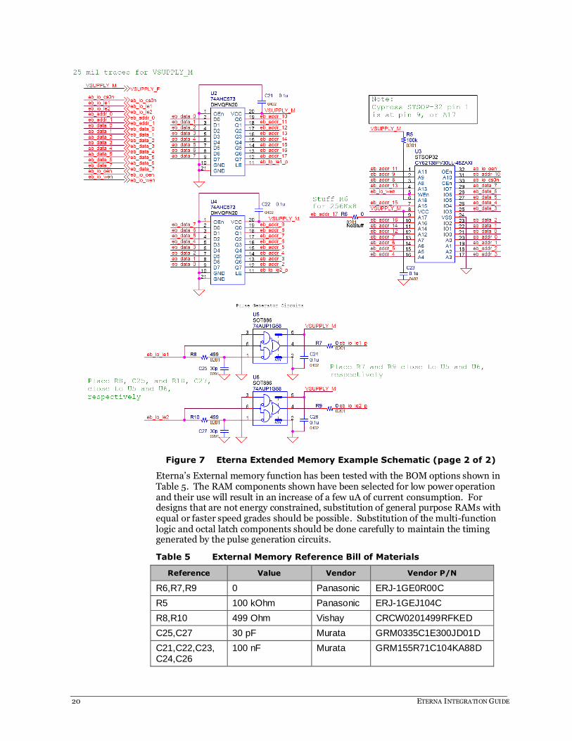
Schematic Design
The schematic shown in Figure 6 and Figure 7 includes all the external connections and components necessary to add the external RAM. The schematic differs from the base schematic shown in Figure 1 in that:
1) CLI access is on UARTC1, not UARTC0
2) Mapping of external bus signals to Eterna’s general purpose function pins
3) The Memory, latches and pulse generators shown in Figure 7
The reference Bill of Materials (BOM) for the addition components needed for the external memory interface is shown in Table 1. Common footprints exist for 128Kbyte, 256Kbyte and 512Kbyte RAMs. While the LTC5800-IPRB only requires 128Kbyte of RAM, it is recommended to include support for 256Kbyte and 512Kbyte RAM variants in the layout, providing flexibility in using alternate equivalent components during manufacture.

ETERNA INTEGRATION GUIDE 19
Figure 6 Eterna Extended Memory Example Schematic (page 1 of 2)
20 ETERNA INTEGRATION GUIDE
Figure 7 Eterna Extended Memory Example Schematic (page 2 of 2)
Eterna’s External memory function has been tested with the BOM options shown in Table 5. The RAM components shown have been selected for low power operation and their use will result in an increase of a few uA of current consumption. For designs that are not energy constrained, substitution of general purpose RAMs with equal or faster speed grades should be possible. Substitution of the multi-function logic and octal latch components should be done carefully to maintain the timing generated by the pulse generation circuits.
Table 5 External Memory Reference Bill of Materials
Reference Value Vendor Vendor P/N
R6,R7,R9 0 Panasonic ERJ-1GE0R00C
R5 100 kOhm Panasonic ERJ-1GEJ104C
R8,R10 499 Ohm Vishay CRCW0201499RFKED
C25,C27 30 pF Murata GRM0335C1E300JD01D
C21,C22,C23, C24,C26
100 nF Murata GRM155R71C104KA88D
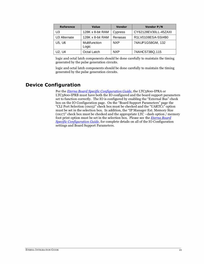
ETERNA INTEGRATION GUIDE 21
Reference Value Vendor Vendor P/N
U3 128K x 8-bit RAM Cypress CY62128EV30LL-45ZAXI
U3 Alternate 128K x 8-bit RAM Renasas R1LV0108ESA-5SI#B0
U5, U6 Multifunction Logic
NXP 74AUP1G58GM, 132
U2, U4 Octal Latch NXP 74AHC573BQ,115
logic and octal latch components should be done carefully to maintain the timing generated by the pulse generation circuits.
logic and octal latch components should be done carefully to maintain the timing generated by the pulse generation circuits.
Device Configuration
Per the Eterna Board Specific Configuration Guide, the LTC5800-IPRA or LTC5800-IPRB must have both the IO configured and the board support parameters set to function correctly. The IO is configured by enabling the “External Bus” check box on the IO Configuration page. On the “Board Support Parameters” page the “CLI Port Selection (0x03)” check box must be checked and the “UARTC1” option must be set in the selection box. In addition, the “IP Manager Ext. Memory Size (0x17)” check box must be checked and the appropriate LTC –dash option / memory foot print option must be set in the selection box. Please see the Eterna Board Specific Configuration Guide, for complete details on all of the IO Configuration settings and Board Support Parameters.

22 ETERNA INTEGRATION GUIDE
Trademarks
SmartMesh Industrial and Eterna are trademarks of Dust Networks, Inc. The Dust Networks logo, Dust, Dust Networks, and SmartMesh are registered trademarks of Dust Networks, Inc. The Linear logo is a registered trademark of Linear Technology Corporation. All third-party brand and product names are the trademarks of their respective owners and are used solely for informational purposes.
ARM and Cortex are trademarks or registered trademarks of ARM Limited in the EU and other countries.
Copyright
This documentation is protected by United States and international copyright and other intellectual and industrial property laws. It is solely owned by Dust Networks, Inc. and its licensors and is distributed under a restrictive license. This product, or any portion thereof, may not be used, copied, modified, reverse assembled, reverse compiled, reverse engineered, distributed, or redistributed in any form by any means without the prior written authorization of Dust Networks, Inc.
RESTRICTED RIGHTS: Use, duplication, or disclosure by the U.S. Government is subject to restrictions of FAR 52.227-14(g) (2)(6/87) and FAR 52.227-19(6/87), or DFAR 252.227-7015 (b)(6/95) and DFAR 227.7202-3(a), and any and all similar and successor legislation and regulation.
Disclaimer
This documentation is provided “as is” without warranty of any kind, either expressed or implied, including but not lim ited to, the implied warranties of merchantability or fitness for a particular purpose.
This documentation might include technical inaccuracies or other errors. Corrections and improvements might be incorporated in new versions of the documentation.
Dust Networks does not assume any liability arising out of the application or use of any products or services and specifically disclaims any and all liability, including without limitation consequential or incidental damages.
Dust Networks products are not designed for use in life support appliances, devices, or other systems where malfunction can reasonably be expected to result in significant personal injury to the user, or as a critical component in any life support device or system whose failure to perform can be reasonably expected to cause the failure of the life support device or system, or to affect its safety or effectiveness. Dust Networks customers using or selling these products for use in such applications do so at their own risk and agree to fully indemnify and hold Dust Networks and its officers, employees, subsidiaries, affiliates, and distributors harmless against all claims, costs, damages, and expenses, and reasonable attorney fees arising out of, directly or indirectly, any claim of personal injury or death associated with such unintended or unauthorized use, even if such claim alleges that Dust Networks was negligent regarding the design or manufacture of its products.
Dust Networks reserves the right to make corrections, modifications, enhancements, improvements, and other changes to its products or services at any time and to discontinue any product or service without notice. Customers should obtain the latest relevant information before placing orders and should verify that such information is current and complete. All products are sold subject to Dust Network's terms and conditions of sale supplied at the time of order acknowledgment or sale.
Dust Networks does not warrant or represent that any license, either express or implied, is granted under any Dust Networks patent right, copyright, mask work right, or other Dust Networks intellectual property right relating to any combination, machine, or process in which Dust Networks products or services are used. Information published by Dust Networks regarding third-party products or services does not constitute a license from Dust Networks to use such products or services or a warranty or endorsement thereof. Use of such information may require a license from a third party under the patents or other intellectual property of the third party, or a license from Dust Networks under the patents or other intellectual property of Dust Network s.
Dust Networks, Inc is a wholly owned subsidiary of Linear Technology Corporation.
© Dust Networks, Inc. 2012 through 2015. All Rights Reserved.
Document Number: 040-0102 Eterna Integration Guide
Last Revised: June 11, 2015
Document Status Product Status Definition
Advanced Information Planned or under
development
This document contains the design specifications for product development. Dust
Networks reserves the right to change specifications in any manner without notice.
Preliminary Engineering samples
and pre-production prototypes
This document contains preliminary data; supplementary data will be published at a
later date. Dust Networks reserves the right to make changes at any time without notice in order to improve design and supply the best possible product. The product is not fully qualified at this point.
No identification noted Full Production This document contains the final specifications. Dust Networks reserves the right to make changes at any time without notice in order to improve design and supply the
best possible product.
Obsolete Not in production This document contains specifications for a product that has been discontinued by Dust Networks. The document is printed for reference information only.

ETERNA INTEGRATION GUIDE 23