inverting sepic reference design for noise sensitive loads
TRANSCRIPT

1TIDT024–December 2018Submit Documentation Feedback
Copyright © 2018, Texas Instruments Incorporated
Inverting SEPIC Reference Design for Noise Sensitive Loads
Test Report: PMP30487Inverting SEPIC Reference Design for Noise SensitiveLoads
DescriptionThis reference design is an inverting SEPIC (Cuk) Converter powering 50-W continuous and up to 70-W peak.The used Cuk topology provides continuous currents at input and output, which allows the lowest conductedemissions in both directions. Compared to an inverting flyback radiated emissions are low as well due to no RFringing at the switch node.
An IMPORTANT NOTICE at the end of this TI reference design addresses authorized use, intellectual property matters and otherimportant disclaimers and information.

Test Prerequisites www.ti.com
2 TIDT024–December 2018Submit Documentation Feedback
Copyright © 2018, Texas Instruments Incorporated
Inverting SEPIC Reference Design for Noise Sensitive Loads
1 Test Prerequisites
1.1 Voltage and Current Requirements
Table 1. Voltage and Current Requirements
PARAMETER SPECIFICATIONSVIN 36 VVOUT -36 VNominal switchingfrequency 200 kHz
Output Current 2 A
1.2 ConsiderationsThe inductor for that design is a modified (footprint, coupling) of the shelf inductor. Except for loadtransient measurements, resistive load were used. Unless otherwise indicated the input voltage was set to36 V. The circuit switches on at about 32.7 V and switches off at a voltage about 27.5V

www.ti.com Testing and Results
3TIDT024–December 2018Submit Documentation Feedback
Copyright © 2018, Texas Instruments Incorporated
Inverting SEPIC Reference Design for Noise Sensitive Loads
2 Testing and Results
2.1 Efficiency Graphs
Figure 1. Efficiency and Loss vs Output Current (VIN =36V)

Testing and Results www.ti.com
4 TIDT024–December 2018Submit Documentation Feedback
Copyright © 2018, Texas Instruments Incorporated
Inverting SEPIC Reference Design for Noise Sensitive Loads
2.2 Load Regulation
Figure 2. Output Voltage vs Output Current (VIN =36 V)

www.ti.com Testing and Results
5TIDT024–December 2018Submit Documentation Feedback
Copyright © 2018, Texas Instruments Incorporated
Inverting SEPIC Reference Design for Noise Sensitive Loads
2.3 Line Regulation
Figure 3. Output Voltage vs Input Voltage (IOUT=1.5A)
Testing and Results www.ti.com
6 TIDT024–December 2018Submit Documentation Feedback
Copyright © 2018, Texas Instruments Incorporated
Inverting SEPIC Reference Design for Noise Sensitive Loads
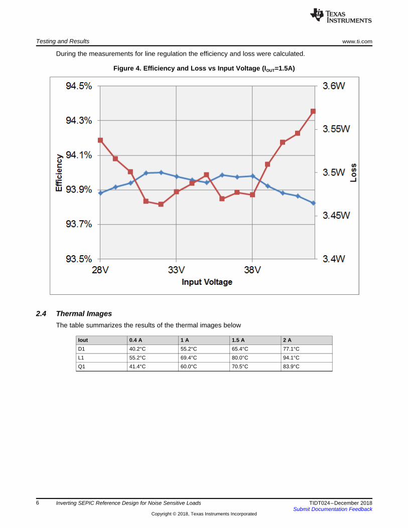
During the measurements for line regulation the efficiency and loss were calculated.
Figure 4. Efficiency and Loss vs Input Voltage (IOUT=1.5A)
2.4 Thermal ImagesThe table summarizes the results of the thermal images below
Iout 0.4 A 1 A 1.5 A 2 AD1 40.2°C 55.2°C 65.4°C 77.1°CL1 55.2°C 69.4°C 80.0°C 94.1°CQ1 41.4°C 60.0°C 70.5°C 83.9°C

www.ti.com Testing and Results
7TIDT024–December 2018Submit Documentation Feedback
Copyright © 2018, Texas Instruments Incorporated
Inverting SEPIC Reference Design for Noise Sensitive Loads
2.4.1 0.4A Output Current
Figure 5. Thermal Image for 0.4 A Output Current
2.4.2 1A Output Current
Figure 6. Thermal Image for 1 A Output Current

Testing and Results www.ti.com
8 TIDT024–December 2018Submit Documentation Feedback
Copyright © 2018, Texas Instruments Incorporated
Inverting SEPIC Reference Design for Noise Sensitive Loads
2.4.3 1.5 A Output Current
Figure 7. Thermal Image for 1.5 A Output Current
2.4.4 2 A Output Current
Figure 8. Thermal Image for 2 A Output Current

www.ti.com Waveforms
9TIDT024–December 2018Submit Documentation Feedback
Copyright © 2018, Texas Instruments Incorporated
Inverting SEPIC Reference Design for Noise Sensitive Loads
3 Waveforms
3.1 SwitchingAll waveforms in this section are measured with full bandwidth. The output current was set to 2 A.
3.1.1 Diode D1
Figure 9. Switch Node Voltage Diode D1
• 20V/div• 1µs/div
• 50ns/major div

Waveforms www.ti.com
10 TIDT024–December 2018Submit Documentation Feedback
Copyright © 2018, Texas Instruments Incorporated
Inverting SEPIC Reference Design for Noise Sensitive Loads
3.1.2 Transistor Q1
3.1.2.1 Drain to Source
Figure 10. Drain to Source
• 20V/div• 1µs/div
• 50ns/major div

www.ti.com Waveforms
11TIDT024–December 2018Submit Documentation Feedback
Copyright © 2018, Texas Instruments Incorporated
Inverting SEPIC Reference Design for Noise Sensitive Loads
3.1.2.2 Gate to Source
Figure 11. Gate to Source
• 2V/div• 1µs/div
• 50ns/ major div

Waveforms www.ti.com
12 TIDT024–December 2018Submit Documentation Feedback
Copyright © 2018, Texas Instruments Incorporated
Inverting SEPIC Reference Design for Noise Sensitive Loads
3.2 Output Voltage RippleThe output ripple waveform was measured direct on the terminal block.
Figure 12. Output Ripple @ 2A IOUT
• 50mV/div (20MHz bandwidth filter)• 1µs/div

www.ti.com Waveforms
13TIDT024–December 2018Submit Documentation Feedback
Copyright © 2018, Texas Instruments Incorporated
Inverting SEPIC Reference Design for Noise Sensitive Loads
3.3 Input Ripple VoltageThe input ripple waveform was measured direct on the terminal block.
Figure 13. Input Ripple @ 2 A IOUT
• 50mV/div (20MHz bandwidth filter)• 1µs/div

Waveforms www.ti.com
14 TIDT024–December 2018Submit Documentation Feedback
Copyright © 2018, Texas Instruments Incorporated
Inverting SEPIC Reference Design for Noise Sensitive Loads
3.4 Bode PlotThe bode box for 10Hz to 1kHz were used for these measurements.
Figure 14. Bode Plot for 36 V Input Voltage and 1.5 A Output Current
Bandwidth (kHz) 1.28Phase margin 81ºslope (20dB/decade) -1
gain margin (dB) -21.4slope (20dB/decade) -0.63freq (kHz) 13.7

www.ti.com Waveforms
15TIDT024–December 2018Submit Documentation Feedback
Copyright © 2018, Texas Instruments Incorporated
Inverting SEPIC Reference Design for Noise Sensitive Loads
3.5 Load Transients
Figure 15. Transient Response for Loadstep from 1 A to 2 A
• channel 1 (blue): Output Voltage => 50mV/div AC (20MHz bandwidth filter)• channel 2 (red): Output Current => 1A/div (20MHz bandwidth filter)• 2ms/div

Waveforms www.ti.com
16 TIDT024–December 2018Submit Documentation Feedback
Copyright © 2018, Texas Instruments Incorporated
Inverting SEPIC Reference Design for Noise Sensitive Loads
3.6 Start-up SequenceThe power supply was plugged in.
Figure 16. Start-up with 2 A Output Current
• channel 1 (blue): Input Voltage => 10V/div (20MHz bandwidth filter)• channel 2 (green): Output Voltage => 10V/div (20MHz bandwidth filter)• 4ms/div

www.ti.com Waveforms
17TIDT024–December 2018Submit Documentation Feedback
Copyright © 2018, Texas Instruments Incorporated
Inverting SEPIC Reference Design for Noise Sensitive Loads
3.7 Shutdown SequenceThe power supply was disconnected.
Figure 17. Shutdown with 2 A Output Current
• channel 1 (blue): Input Voltage => 10V/div (20MHz bandwidth filter)• channel 2 (green): Output Voltage => 10V/div (20MHz bandwidth filter)• 2ms/div

IMPORTANT NOTICE AND DISCLAIMERTI PROVIDES TECHNICAL AND RELIABILITY DATA (INCLUDING DATASHEETS), DESIGN RESOURCES (INCLUDING REFERENCEDESIGNS), APPLICATION OR OTHER DESIGN ADVICE, WEB TOOLS, SAFETY INFORMATION, AND OTHER RESOURCES “AS IS”AND WITH ALL FAULTS, AND DISCLAIMS ALL WARRANTIES, EXPRESS AND IMPLIED, INCLUDING WITHOUT LIMITATION ANYIMPLIED WARRANTIES OF MERCHANTABILITY, FITNESS FOR A PARTICULAR PURPOSE OR NON-INFRINGEMENT OF THIRDPARTY INTELLECTUAL PROPERTY RIGHTS.These resources are intended for skilled developers designing with TI products. You are solely responsible for (1) selecting the appropriateTI products for your application, (2) designing, validating and testing your application, and (3) ensuring your application meets applicablestandards, and any other safety, security, or other requirements. These resources are subject to change without notice. TI grants youpermission to use these resources only for development of an application that uses the TI products described in the resource. Otherreproduction and display of these resources is prohibited. No license is granted to any other TI intellectual property right or to any third partyintellectual property right. TI disclaims responsibility for, and you will fully indemnify TI and its representatives against, any claims, damages,costs, losses, and liabilities arising out of your use of these resources.TI’s products are provided subject to TI’s Terms of Sale (https:www.ti.com/legal/termsofsale.html) or other applicable terms available eitheron ti.com or provided in conjunction with such TI products. TI’s provision of these resources does not expand or otherwise alter TI’sapplicable warranties or warranty disclaimers for TI products.IMPORTANT NOTICE
Mailing Address: Texas Instruments, Post Office Box 655303, Dallas, Texas 75265Copyright © 2021, Texas Instruments Incorporated