euv lithography : historical perspective and road ahead · presented on september 19, 2014 at...
TRANSCRIPT

EUV lithography : historical perspective and road ahead
Banine, V.Y.
Published: 01/01/2014
Document VersionPublisher’s PDF, also known as Version of Record (includes final page, issue and volume numbers)
Please check the document version of this publication:
• A submitted manuscript is the author's version of the article upon submission and before peer-review. There can be important differencesbetween the submitted version and the official published version of record. People interested in the research are advised to contact theauthor for the final version of the publication, or visit the DOI to the publisher's website.• The final author version and the galley proof are versions of the publication after peer review.• The final published version features the final layout of the paper including the volume, issue and page numbers.
Link to publication
General rightsCopyright and moral rights for the publications made accessible in the public portal are retained by the authors and/or other copyright ownersand it is a condition of accessing publications that users recognise and abide by the legal requirements associated with these rights.
• Users may download and print one copy of any publication from the public portal for the purpose of private study or research. • You may not further distribute the material or use it for any profit-making activity or commercial gain • You may freely distribute the URL identifying the publication in the public portal ?
Take down policyIf you believe that this document breaches copyright please contact us providing details, and we will remove access to the work immediatelyand investigate your claim.
Download date: 01. Aug. 2018

Visiting addressDen Dolech 25612 AZ EindhovenThe Netherlands
Postal addressP.O.Box 5135600 MB Eindhoven The Netherlands
Tel. +31 40 247 91 11www.tue.nl/map
Where innovation starts
/ Department of Applied Physics
Inaugural lecture
Prof. Vadim Banine
September 19, 2014
EUV LithographyHistorical perspective and road ahead

Presented on September 19, 2014at Eindhoven University of Technology
Inaugural lecture prof. Vadim Banine
EUV Lithography Historical perspective and road ahead


3
“Any sufficiently advanced technology is indistinguishable from magic” Third law of Arthur C. Clarke
Ladies and gentlemen,The main topic of my lecture will be the physics and technology of nano-lithography and extreme ultraviolet lithography(EUVL) in particular. Looking from a historical perspective I will attempt to sketch possible trends and opportunitiesfor scientific advancement in the chosen area and share my experience of co-operation between industry and scientific institutes as well as the lessons I learned from it.
In my presentation I will refer frequently to the empirical laws, such as Moore’s orKoomey’s, which are mostly governed by economic developments without goinginto details of economics due to a lack of any thorough economic knowledge andleaving this subject to the specialists such as Adam Smith, Karl Marx, AlanGreenspan and Francis Fukuyama.
I will also use statistical material, knowing all too well the scientific ambiguity ofsuch an approach based on uncertainty of both data collection and the datainterpretation. Thus statistical material will be used for illustration purposes only.
Introduction
Figure 1
From carved printing [1] through rotary press [2] to Photolithography and EUVL [3], [4], [5]

4 prof. Vadim Banine
Lithography in the form of the carved type printing can be dated as far back as the3rd century AD.
Starting from the 19th century lithography played a major role as the basis fordissemination and preservation of the knowledge in the form of printed books,maps, newspapers etc. In the mid 20th century, with the invention of the micro-and nano-electronics, it took on a new meaning and became the basis for thepatterning solutions of the modern day semiconductor industry. This by itselfincreased the creation and dissemination of knowledge exponentially, which in itsturn fuels further progress in technology.
For 50 years the progress of semiconductor industry and thus lithography wasgoverned by the law named after a founder of Fairchild Semiconductors and laterco-founder of Intel, G. Moore.
Though it has been reformulated several times, Moore’s law basically states thatthe number of transistors on integrated circuit doubles every 1.5-2 years. Thoughit is not an exact law as, for example the 2nd law of Newton, and at best can becalled an economic law or a conjecture, based on a couple of points over a periodof 6 years (see Figure 2), the prediction of Moore has proved to be true for the last50 years.
Figure 2
Left in the figure is the famous publication of the graph, which is later became knownas Moore’s law [6]; Right in the figure is a picture of several out of thousands ofMoore’s law representations on Google search in 2014

5EUV Lithography: Historical perspective and road ahead
Almost every year prominent technologists and scientists come up with aprediction concerning the end of the Moore’s law. Quoting the NY Times in 1997:“… the question keeps arising of whether Moore’s law will lapse in the next decadeor so, ending the era of explosive growth.” A similar article appeared in the NYTimes in 2003. In 2005 L. Penenberg in Slate wrote: “Unless chip manufacturersfigure out some new techniques the march to miniaturization could stall”. Similarclaims came in 2008 and in 2014 at SPIE conferences. Though it is difficult toimagine that such aggressive scaling will continue indefinitely, one cannot butthink about the 1st law established by Arthur C. Clarke:
“When a distinguished but elderly scientist states that something is possible, he isalmost certainly right. When he states that something is impossible, he is veryprobably wrong.”
Although the past track of a development is no insurance for its continuation inthe future, it is worthwhile mentioning that it is possible to extend the exponentialtrend of Moore retrospectively back to 1900 as was done by Ray Kurzweil [7].
Looking around, everyone can see the technological change our society hasexperienced in the last 50 years due to the industry driving and competing alongthe road set by Moore. We have seen a significant paradigm shift of employmentof technology from:
Figure 3
Trend of the technological advances of computers according to R. Kurzweil incalculations per s per 1000$ (data are taken from [7])

6 prof. Vadim Banine
• connecting different locations e.g. land-line telephones, to • connecting individuals e.g. mobile phones and to • connecting smart things and devices in the near future e.g. automotive, home
appliances, medical etc. (or as it called nowadays: “internet of things”)
This is nicely illustrated in [8].
Another trend, which governs semiconductor progress, is related to powerconsumption.
The more computational technology embedded in our society, the higher thepercentage of power consumption is dedicated to it. Till 2005 making transistorssmaller and at the same time increasing the clock speed (so-called Dennardscaling) went hand in hand. This simultaneously allowed a decrease in the chipcost and a rather straightforward increase of computer performance. In 2005 thistype of scaling came to an end. One of the contributing factors to this was the
Figure 4
Koomey’s-Moore’s law for computation per kWatt [10]

7EUV Lithography: Historical perspective and road ahead
excessive power requirement of the computer chips while the wide spread use ofmobile devices prompted another push for more power-efficient technologies.
One more fact, related to power consumption, has to be taken into account aswell. Though evaluations differ, currently server farms alone already account for atleast a couple of percent of the electrical power consumption in the US [9, 10].
Thus scalability of the power efficiency of computations becomes a significantadditional driver for Moore’s law. As has been shown in [10] the dependence ofcomputations per kWh as a function of time have a familiar Moore’s like behavior,which is sometimes called Koomey’s law, see Figure 4.

8
As has been stated above lithography is one of the most important components ofthe progress of semiconductor technology. Figure 5 is a sketch of thesemiconductor process with the end product a working chip. It starts withmanufacturing of a silicon wafer, whose diameter has changed over the years from 100 mm in 1975 to 150 mm in 1980 and 200 mm 1990 to the current size of300 mm. The next step after wafer polishing, is depositing a certain material onthe wafer, which is coated with a photosensitive photoresist layer. During thelithography step a pattern, printed on the mask (or reticle), is projected onto thephotoresist of the wafer. This process may be familiar to some of the older peoplein the audience: before the era of digital photography and printers, photos weremade using of an optical enlarger in a dark room. While an optical enlargermagnifies the pattern on a film in order to produce larger pictures, the opticallithography systems nowadays de-magnify the pattern by a factor of 4. Similar tothe “dark room” process the photosensitive layer is developed after exposure.Then an etch or implantation step is performed.
Place of lithography in semiconductor technology
Figure 5
Lithography is at the heart of chip manufacturing

9EUV Lithography: Historical perspective and road ahead
This process, repeated 30-50 times in a layer by layer way, builds up the 3Dstructure of a chip, Figure 6.
Figure 6
A chip under the microscope

10
New challenges to further scale down the critical dimension of semiconductordevices in the 21st century attracted the close attention of both high-techcompanies and scientific institutes to extreme ultra-violet lithography (EUVL).
The number of publications devoted to a certain technological problem by thescientific community can be considered as a sign of this community’s interest inthat particular problem. At the same time, the absolute number of publicationsdoes not directly correspond to the problem’s significance. In order to illustratethis one can apply a uniform search on the Web of Science (WoS) for articles in thefield of interest. As an example, the problem could have been significant enough,such as “Street Lighting” (Nobel Prize 1912), but has by now become quite
Extreme Ultra-violet Lithography
Figure 7
History of Extreme Ultraviolet Lithography (EUVL) [11], [12], [13]

11EUV Lithography: Historical perspective and road ahead
mundane and too developed to attract any significant attention: 785 publicationsover the last 69 years. It is almost equal in count to the search for the“Gravitational Wormhole”: 530 publications over the same period. One mightargue that as exciting and futuristic as such a problem might be (Star Trek), it isvery far from any practical application. A very popular subject and relatively closeto application, however still far from becoming a real wide spread product, wouldbe “Graphene” (Nobel Prize 2010): 56,889 hits on WoS. In this list “ExtremeUltraviolet” scores a decent 10,236 hits on WoS: already applied but still veryinteresting.
As indicated in [11], the region between ultraviolet and X-ray is one of the lastregions of the electromagnetic spectrum to be developed and to find a practicalapplication. As can be seen from the chart in figure 7, the number of publishedarticles mentioning this part of the spectrum remained relatively low till the end ofthe 1980’s. Unlike EUV, both X-ray and ultraviolet have a significantly longerabsorption length. EUV is absorbed in nanometers of any solid material andmicrometers under normal conditions in gases. This defines a high threshold fortechnology, which one has to use in such an investigation (special multilayerreflective optics, high vacuum, hot 20-50 eV plasma or accelerator technology forproduction of EUV). At the same time, from the application point of view, interesthas been very limited. That being said, one should mention that with the currenttechnological achievements in the area opportunities for the investigation ofmaterials in EUV might be quite promising, as is evident in the work of WeilunChao et al on Soft X-ray microscopy [14]. Also investigation of the EUV spectrum of the sun is important for understanding the evolution of Earth’s ionosphere,predictions of communication system degradation (including GPS) andatmospheric heating.
As one can see, significant technological advances are needed in order to be ableto exploit this part of the spectrum. Such opportunity presented itself at the endof the 1980’s in the form of a new application: EUV lithography. It led to anexplosion of the number of publications at this point in history.
The first paper on the possible application of EUV, or as called at that time soft X-ray, for lithography was published by Bell Labs [15] in 1985. Already in 1989Kinoshiba et al [16] demonstrated EUV imaging in resist with critical dimensions of~ 0.5 µm, using Schwarzschild projection optics and synchrotron as a source. In1991 EUV images were shown by prof. Bijkerk’s group [17]. A laser producedplasma (LPP) source was utilized in order to produce EUV radiation. CDs of

12 prof. Vadim Banine
~60-80 nm were demonstrated in Japan [18] and in the US on an ETS tool [19] in2000 and 2001 respectively. The EUV lithography program was launched at ASMLin 1997. It resulted in the 2006 shipment of two Alpha Demo Tools to R&D facilitiesat IMEC (Belgium) and the University of Albany (NY, USA), which performed on thelevel of 28 nm for the critical dimension (CD) printing. This progressed furthertowards the shipment preproduction systems NXE:3100 and NXE:3300, see e.g.refs [20, 21].
Another interesting trend can be observed from figure 7: while the number ofcitations for EUV lithography peaked in 2007, the total amount of papers inscientific publications has continued its grow till now. This can be taken as a signof the relevance and scientific value of the field of EUV.In order to understand what drives the shift of lithography to EUV from thetechnological point of view, one should consider the formula for the resolution ofoptical lithography:
R = k1λ / NA,
where λ is the wavelength of light, k1 is a coefficient and NA is the numericalaperture of the lens [22]. One can easily see that scaling wavelength isinstrumental in the improvement of the optical resolution. The evolution oflithographic wavelengths has gone from 436 nm (aka g-line) to 365 nm (aka i-line)to 248 nm (aka KrF) to 193 nm (aka ArF) and finally to 13.5 nm (aka EUV). As an
Figure 8
Number of articles found in WoS on lithography made with 365 nm(aka i-line) to 248nm(aka KrF) to 193 nm (aka ArF) and finally to 13.5 nm (aka EUV).

13EUV Lithography: Historical perspective and road ahead
example, for 13.5 nm wavelength, NA of 0.6 and an equal-lines-and-spacespattern, the minimum feature size would correspond to k1 of 0.25 and be equal to~6 nm. This is a significant step down “Moore’s alley”.
Figure 8 describes the evolution of lithographic technology with the wavelengthapplied (i-line: 365 nm; KrF: 248 nm; ArF: 193 nm and EUV: 13.5 nm) in the contextof the scientific material, dedicated to each of the technologies, which can befound at WoS. As one can see, each step forward produced both higher peaks inthe number of articles in the scientific literature and in their total amount than ateach step before. It can be used as an illustration of increased technologicalchallenges as well as investment in the solutions for which scientific methods areneeded. One can argue that it shows a shift from the technological approach in theform of a craft to scientific one.
With the printed feature size of the semiconductors continuously decreasing andnow shifting from the 22 nm to 14 nm node, double patterning (DP) lithographybased on 193 nm deep ultraviolet (DUV) systems is being employed [5]. The nextstep towards extreme ultraviolet lithography (EUVL) is seen as a logical one withrespect to cost reduction in equipment space as well as a carrier for furtherfeature downscaling [6].
Figure 9
Single exposure lines and spaces structure at 13 and 14 nm in various resists:Chemically amplified resist (left) and Inpria resist (right) [24]

14 prof. Vadim Banine
Though this step is economically logical major technological developments areneeded in order to realize it and with it comes extremely exciting science.
EUV lithography already now produces stunning images of a single step exposure,see e.g. [23] and [24]
A major technology change and the realization of hundreds of inventions wereneeded in order to achieve this result.
The three main important differences between EUV and DUV lithography are:• Reflective multilayer (Bragg type) optics instead of refractive optics• Plasma source (laser produced plasma and discharge produced plasma) sources
instead of UV laser• High level of contamination control at the mask as well as in a high-vacuum
environment (instead of normal pressure in DUV)
Reflective optics of EUVDue to the fact that EUV is already being absorbed in a very thin layer, it is notpossible to use refractive optics for this wavelength. Furthermore, the reflectivityof EUV from any surface at normal incidence is quite low (<< 1%). In order torealize an optical system with EUV at 13.5 nm one has to use interference coatingsconsistent with 40-60 Mo-Si pares of layers with a thickness per pair equal toabout 6.7 nm, see Figure 10.
Figure 10
TEM picture of a cross-section of multilayer (Molybdenum-Silicon; MoSi) coating [26]

15EUV Lithography: Historical perspective and road ahead
Furthermore in order to have a good reflection of about 68-70% as well asimaging, the surface of the aspherical mirrors, used in the optical system for thescanner, has to be polished very accurately. For example looking at theperformance of the multilayer Optics [25] in Figure 11, one can see theimprovement of the achieved mirror roughness from 0.25 nm rms in 2004 to 0.05nm rms now. These values are at the level of a single atom!
EUV SourceAt the same time a number of challenges proved to need more attention thanoriginally envisioned. One of those is the EUVL source, see figure 12.
The whole history of the source development can be divided into the main four“ages”:• Age of choice. During this period starting from 1998 till roughly 2001-2002 the
main understanding of the EUVL system was developed. This age also producedthe understanding of the source requirements, in particular the desired power.At the same time a number of EUV production options was investigated [27],such as accelerator technology based [11], laser produced plasma [28, 29, 30,31, 32, 33] and different types of discharge produced plasma sources [34, 35,36, 37, 38, 39, 40, 41]. The level of the power demonstrated at that time was ~ 0.1 W.
Figure 11
Roughness results and target levels for mirrors of different EUVL tool generations andcoated mirror for the NXE:3300B generation.

16 prof. Vadim Banine
• Age of Xe (Xenon). While the understanding of the EUV source requirementsmatured, the list of candidates for the sources narrowed down to Xe laserproduced plasma [31] and discharge pinch plasma sources [34, 36]. Theachieved level of power with Xe source in this period of time (till 2003) was ofthe order of watts. At the end of this period it also became clear that due to alow conversion efficiency (CE) of Xe plasma (< 1% in 2π in 2%-band) the chancefor these sources to achieve 100 W of EUV clean photons after collection (atintermediate focus (IF) [42] is not high. Thus the necessity of change to adifferent EUV “fuel”, namely Sn, was formulated and investigated during thisperiod [42]
• Age of Sn (Tin). Age of Sn or switch of multiple suppliers to the Sn fuel startedin 2003 [32, 33, 35, 37, 41]. The best powers achieved in IF increased by a factorof 5 mainly due to conversion efficiency (CE) increase to the value of 5-6% forSn [41, 43, 44, 45, 46, 47, 48]. The switch to Sn did not only have advantages. Incomparison to Xe, Sn is a rather “dirty” EUV fuel. Thus additional measures hadto be taken while dealing with a decrease in the lifetime of the collector optics.
• Age of industrialization. Right now we are living in the age of industrialization.It started with the delivery of 2 ADT tools with EUV sources based on Sn DPPand proceeded with NXE-3100 and later with NXE-3300 machines. NXE-3100 wasdelivered both with Sn DPP and Sn LPP sources and NXE-3300 with a Sn LPPsource. While peak performances of those sources achieved almost 100 W level[49] the average power and utilization are still a challenge. As can be seen from
Figure 12
History of the source development: power requirements and achievements specifiedas watts at intermediate focus (focal point of collector after all debris mitigationapparatus, spectrally pure) [12].
17EUV Lithography: Historical perspective and road ahead
Figure 12 the power delivered at IF experiences a steady though slower thandesired growth. At the same time the industry remains power hungry and futurerequirements exceeding the 250 W can be expected. In order to make a nextstep in this direction significant and sometimes pioneering research is needed. I will come back to this topic later in this lecture.
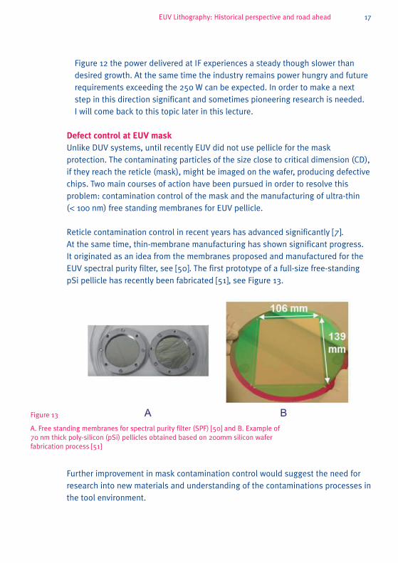
Defect control at EUV maskUnlike DUV systems, until recently EUV did not use pellicle for the maskprotection. The contaminating particles of the size close to critical dimension (CD),if they reach the reticle (mask), might be imaged on the wafer, producing defectivechips. Two main courses of action have been pursued in order to resolve thisproblem: contamination control of the mask and the manufacturing of ultra-thin (< 100 nm) free standing membranes for EUV pellicle.
Reticle contamination control in recent years has advanced significantly [7].At the same time, thin-membrane manufacturing has shown significant progress. It originated as an idea from the membranes proposed and manufactured for theEUV spectral purity filter, see [50]. The first prototype of a full-size free-standingpSi pellicle has recently been fabricated [51], see Figure 13.
Further improvement in mask contamination control would suggest the need forresearch into new materials and understanding of the contaminations processes inthe tool environment.
Figure 13
A. Free standing membranes for spectral purity filter (SPF) [50] and B. Example of 70 nm thick poly-silicon (pSi) pellicles obtained based on 200mm silicon waferfabrication process [51]

18 prof. Vadim Banine
Contamination and erosion control of opticsAs stated above while DUV lithography machines work at normal pressure theoptical path of EUVL apparatus is placed in a high quality vacuum. The reason forthis is twofold: high absorption of EUV in any material including gases (e.g.already at 10 mbar 30% of radiation will be lost after 2 m of optical path) andpossible contamination or erosion of optical surfaces (e.g. already 1 nm of carbondeposition on each optical surface in the exposure tool will lead to an EUV loss of~10%). In order to put it into perspective the required lifetime of the opticalcomponents in future generation EUV lithography tools is specified at 30,000illumination hours. Solutions already provided in the tool, as well as data of theexisting ASML tools at customers, show that the methods used in order tomaintain a high quality vacuum have a positive effect on the lifetime of optics [52].On the other hand because it is not feasible to perform lifetime tests of such longduration, fundamental understanding of the processes that limit the lifetime isrequired. Here is where applied scientific research can be fruitful for the industry.
19
Now I want to try and sketch some emerging challenges of EUV lithography as wellas the possible next steps in its development. I will also attempt to put this in thelong-term perspective of the scientific research needed to fulfill the industry needsas well as provide you with some examples of it.
The future technological advancement can be looked at from two differentperspectives: the scaling of the current EUV lithography at the same wavelength of13.5 nm and going beyond EUV (BEUV) to the next wavelength, as has happened a number of times in the development of lithography.
The technological and concurrent scientific challenges of the “conventional” 13.5 nm EUVL include: • Technologically: higher throughput of the system by achieving more of effective
EUV power from the source and on the other side of the “power duality”,maintaining resist sensitivity growth under control. Scientifically it will mean:understanding of and pushing on the physical limits of the current sources,looking for alternatives and understanding and developing new resists;
• Technologically: tighter control of mask contamination and thus scientifically:better understanding of the mask contamination processes as well as lookingfor new possible solutions;
• Technologically: maintain long optical lifetime at higher powers andscientifically: establish scaling laws of the very long (almost decade) opticaldegradation and finding solutions for it if necessary;
• Technologically: decreasing printable critical dimension by increasing numericalaperture of optics and scientifically: investigating new optical schemes andincreasing quality of the multilayer optics even further
I want to provide the audience with three examples of interesting science, whichcan impact the future development the EUVL technology.
Future of EUVL

20 prof. Vadim Banine
Example 1. Further study on contamination and erosion control of optics
In 2002, while performing an alignment of the EUV optics, John de Kuster, LucStevens and I observed an effect as depicted in figure 14, namely a plume of lightgenerated in the converging EUV beam in the residual argon gas, something thathas been observed later in other gases as well.
By itself the plasma created under the conditions of EUVL is an interesting objectof scientific study. It is created without any discharge, whether optical or electrical,under low pressure and characterized by low density and temperature on the onehand, and is visually localized on the other hand. Plasmas, produced in such away, are not very well investigated outside EUV studies.
The existence of light by itself does not cause any significant effect onto theperformance of the EUV system. The plasma created in EUV might on the otherhand have an impact on the surface processes as well as processes in the bulk ofthe machine [53]. The effects and characteristics of plasma are described briefly in[54], where it has been demonstrated that in the long term it might have abeneficial self-cleaning effect for EUVL optics. Due to the very long lifetimes(about 7 years) required by the optics, as mentioned before, direct experimentsare virtually impossible. Thus scaling laws have to be established in order topredict the impact of some subtle effects for very long exposures, hardlymeasurable in relatively short experiments. This study is being performed in thecooperation between ASML, prof. F. Bijkerk’s group at the University of Twente, thegroup of prof. G. Kroesen at TU/e and a group of prof. K. Koshelev at ISAN.Another effect of EUV induced plasma on tool performance is the creation andbehavior of particles in the tool, which is relevant for the study of defectivity, asmentioned above. This is now being investigated by the group of prof. G. Kroesenat TU/e .
Figure 14
Plasma created in the EUV converging beam in rest Ar gas.

21EUV Lithography: Historical perspective and road ahead
Example 2. Further study on EUV sourcesThe main path for the EUV source development is LPP. High, close to theoretical,CE has already been shown in the low repetition rate systems [45-48]. Also thedevelopment of the high power CO2 lasers proved to be an achievable target andlasers already installed in the field are operating at 22 kW [24]. The intermediatepath lies along achieving stable operation in industrial installations with provenparameters or being optimized in low power laboratory experiments. In thesomewhat distant future, possibly beyond this decennium, even high powerrequirements should be fulfilled. The sources for those power requirements couldbe in the modifications of existing industrial solutions with more effective lasersand target shaping or completely different types of sources. Let us consider one ofthose: free electron laser in a “shoe box”. While Free Electron Lasers (FEL) havebeen considered for EUVL application for the last 10 years [55, 56, 57] it remainsboth a potentially promising yet a very large and expensive machine. Recently anumber of articles appeared that exploited the principles of micro-fabricateddielectric laser accelerators or laser wake field acceleration of a tabletop size,which might in the distant future substitute the lengthy accelerators [58], [59].Alternative FEL mechanisms have also been proposed in [60] and furtherinvestigated in [61]. Though those techniques signify only the first steps, thefuture of those might be very exciting both scientifically and technologically.
Example 3. Beyond-EUVAdaption of the current system to the new wavelength forms a technological andscientific challenge whereby the wavelength choice is dictated by the availablereflective multilayer optics and source.
If looking at scaling beyond 7 nm node and 2020 another wavelength of around6.7-6.8 nm can be considered [27]. Using the same formula as before for theresolution of optical lithography, one can conclude that the corresponding bestachievable resolution for 6.7 nm wavelength is ~ 3 nm.At the same time, the development of such a system meets significant challengescompared to the existing 13.5 nm, as mentioned in [27]:• New multilayer material process with e.g. La and B pairs and larger number of
pairs (~200 vs 60 for 13.5nm)• Significantly better (~λ2) polishing of the substrates to reduce stray light• Dealing with a narrower spectral bandwidth (~0.5% vs 2% for 13.5 nm) both for
high angular spread mirrors and an effective EUV radiation coupling of thesource
• New “fuel” for the source management, e.g. gadolinium (Gd) or new source

22 prof. Vadim Banine
In the initial experiments by IPM/Phystex a single mirror reflectivity of ~ 44% wasachieved against the theoretically achievable ~ 80%. For comparison the achievedvalues for 13.5 nm multilayer are ~72-73%. The theoretical value for 6.xmultilayers exceeds this of “13.5 nm” but the actual achieved value at that timewas significantly lower. The work of multiple groups in recent years has managedto narrow this gap, see figure 15. By 2012 the reflectivity achieved in the group ofprof. Fred Bijkerk of the University of Twente was ~50% [62]. Lately anothersignificant step in this direction has been made by the same group, whichexceeded the reflectivity barrier of 60% [63]. Nevertheless, further effort to bridgethe gap is needed.
As shown in [23], the highest conversion efficiency in-band (CE) achieved for theGd fuel for LPP by ISAN is ~1.8%. That is already a significant value but animprovement has to be made to reach the best value of CE for Sn of 5-6%, seeabove. Another possibility here is to use FEL techniques mentioned above.Looking at the graph of publications with respect to BEUV lithography with theuniform search in WoS for both 13.x and 6.x nm one can see that 6.x nm is at thebeginning of its scientific period in comparison with 13.x nm, see figure 16. It isworthwhile mentioning that these analyses have an indicative value only, and arenot scientifically accurate.
Figure 15
Achievements of reflectivity for 6.x nm ML mirror. Summary of groups of IPM/Phystex,the University of Twente and Rigaku [62, 63]

23EUV Lithography: Historical perspective and road ahead
Figure 16
Relative amount of publications per year in 13.x and 6.x nm as a possibility forlithographic application

24
In the last 17 years working at ASML in co-operation with scientific universities andinstitutions I have learned a number of valuable lessons on the efficiency ofresearch and technology project settings.
1. Research in EUV lithography requires a massive amount of investment. EUVphotons are very expensive. This means that it is difficult for one university orlaboratory to perform such investigation without significant backing fromgovernment and industry (e.g. EUV LLC). On the other hand there is anextensive list of successful co-operations, where different universities andinstitutes combine their expertise and infrastructure for EUV. Here are just a few of them:a. So called “Flying circus” cross-measurement of EUV sources in the early
days of EUVL has been performed in close co-operation between ASML,FOM Institute of Rijnhuizen and Philips Research with the aid of Carl ZeissLLNL and Bessy, see e.g. [64].
b. Co-operation between ASML, TU/e and ISAN on the EUV sources, see e.g.[65]
c. Co-operation between FOM Institute Differ, ISAN and MESA+ of theUniversity of Twente on EUV induced plasma, [54].
2. From my point of view, the most useful research work on EUVL, which can befound at a later stage in the technological applications, occurs in close co-operation with the industry. Such co-operations are most fruitful, when anumber of (PhD) students and scientists of a particular research institute oruniversity are located (at least part time) in industry laboratories. This allowsfor a clear setting of the purpose of a research study, preserving the scientificvalue of it. Examples are:a. Long-term cooperation between TU/e and ASML, which has produced
highly valuable work by the PhD students:i. E. Kieft (cum laude)ii. K. Gielisseniii. M. van der Veldeniv. N. Lammers and currently
Working together: Universities and Industry

25EUV Lithography: Historical perspective and road ahead
v. R. van der Horstvi. F. van de Wettering and many others
b. CP3E FOM IPP project between ASML, Carl Zeiss, Differ/ FOM Rijnhuizen,and ISAN as well as many years of co-operation between those groupsbefore and after CP3E in the form of “Focus group” during which a number(6-8) of students were located at ASML’s premises.
c. 14 year cooperation between ASML and ISAN, with frequent exchange ofstudents and scientists.
Again, the list of such cooperations is much more extensive than the list ofexamples above.
3. Every manager can lead a limited amount of projects, whether small or large,with sufficient quality (law of Benschop). Due to the fact that small projectstake about the same time to manage as the large ones, it is important to findpartners able solve a substantial part of the problem on their own and, ifneeded, with a large number of scientists and at separate locations. Thisusually contradicts the tendency of a scientific institute to think in terms ofsmall (1-2 PhDs) projects, often confined to a group in a faculty, while theindustry has to take care of the coherence and synergy of those multipleprojects. Still it is not an impossible task to find such parties. An example of suchsuccessful cooperations is that between ASML, Carl Zeiss and FOM Rijnhuizenor ASML and ISAN. Also recently ARCNL, which will follow along this road, hasbeen found.
4. Ease of cooperation, in my experience, is a threshold function of geographicaldistance between the cooperating parties (or, in other words the possibility to meet at very short notice). If the travel time between the parties exceeds 1 hour, the co-operation is not much easier than when it is 5 hours or more,but it is significantly easier when it is 20 minutes or less. This should not stand in the way of approaching remote institutes with arelevant competence. The time lag can be mitigated by regular exchange ofresearchers between the parties involved.
5. It is my observation that technological development in a company does notfollow the same lines academic-research. Technological development reliesmuch more on craft and not always on deep understanding of the matter. Alsothe best exciting scientific solution cannot always be implemented in theapplication due to engineering or the business limitations of a complete

26 prof. Vadim Banine
system. This has to be understood and permanently calibrated by the co-operating parties. On the other hand if successful, it often brings bothtechnological success and scientific advancement; see point 2 and 3 above. It is also worth mentioning that sometimes a scientific finding, which looksridiculous from the common sense point of view, still find a way at a certainmoment into technology if the need is high enough, e.g. [50]. Some patience isadvisable from both sides in such cases.
6. The speed of development in the industry is sometimes much higher than thatat a scientific institute mostly due to the amount of resources that the industrycan focus on a solution of a certain prevailing problem. This is why it isadvisable from the beginning for the scientific institution to select a researchtopic that preferably has a horizon of approximately ten years, is out of thescope of the immediate attention of industry but will contribute to its future.
I want to finish with another quote of Arthur C. Clarke (the 2nd law of AC):
“The only way of discovering the limits of the possible is to venture a little waypast them into the impossible.”

27
In closing I would like to take the opportunity to extend my sincerest appreciationfor the support that I have received from colleagues, friends and family.
Firstly, I am grateful to my employer of the last 17 years ASML and in particular toJos Benschop, SVP Technology, for his trust and ongoing professional support inthis endeavor.
I am much indebted to my colleagues at ASML and scientists, with whom I collaborated in the various projects around the world. The complete list of those,whom I worked with during all this years, learned from and owed to might exceedthe text of the lecture itself. Thanks for all your help.
At TU/e, I would like to offer my special thanks to Prof. Gerrit Kroesen, Dean of the Department of Applied Physics. He has been a driving force behind thisappointment. Also thank you for all the useful advice you have given me in the last 23 years we have known each other.
To my tutor at TU/e Bram Veefkind: thank you for helping me to find my way frommy very first steps on Dutch soil.
I also cherish and feel lucky to have a good friend and collaborator KonstantinKoshelev of ISAN. I have learned a lot from you. You are a true inspiration to me.
Finally, this whole thing would make little sense to me without my family. I want tothank my mother. You made me who I am. My wife, Hanneke, I know how manytimes I disturbed the delicate balance between my work and everything else thatmatters. Thank you for bringing me back to my senses time after time. Thank youto my son, Misha, in whom I reflect and who helps me to understand myself.
Ik heb gezegd.
Acknowledgments
28
1. China Culture. (n.d.). Retrieved from http://ww1.chinaculture.org/gb/en_aboutchina/2003-09/24/content_26509.htm
2. “Rotary Printing Press.” Wikipedia. Wikimedia Foundation, 13 July 2014. Web.20 July 2014.
3. “CPU-World.com Forums :: View Topic - My First Attempts to Take Die Shots.”CPU-World.com Forums :: View Topic - My First Attempts to Take Die Shots.Web. 20 July 2014.
4. http://phys.org/news135270280/5. “Advanced Search.” ASML: Products. Web. 20 July 2014.6. Moore, G.E. (1965, April). Cramming More Components onto Integrated
Circuits. Electronics , pp. 114-1177. http://www.singularity.com/charts/page67.
http://content.time.com/time/magazine/article/0,9171,2048299,00.html8. Ericson, Presentation, ISS Europe, Feb 20119. http://enduse.lbl.gov/projects/InfoTech.html10. Koomey, Jonathan G., Stephen Berard, et al. “Implications of Historical
Trends in The Electrical Efficiency of Computing.” IEEE Annals of the Historyof Computing. vol. 33, no. 3. July-September. pp. 46-54. (2011)
11. Attwood, David T. Soft X-rays and Extreme Ultraviolet Radiation: Principlesand Applications. Cambridge: Cambridge UP, 2000. Print
12. Banine, Vadim. “EUV Lithography: Today and Tomorrow.” Future Trends inMicroelectronics: Frontiers and Innovations. By Serge Luryi, Jimmy Xu, andAlex Zaslavsky. Wiley-IEEE Press, 2013
13. “Multiwavelength Sun.” Multiwavelength Sun. Web. 20 July 2014.14. W. Chao et al, Nature 435, 1210-1213 (30 June 2005)15. K. Hoh and H. Tanino, Bell electrotech. Lab., 49 (1985) 4716. H. Kinoshota, K. Kurihara et al. J. Vac. Sci. Technol. B 7 (1989) 164817. F. Bijkerk, et al., “Design of an extended image field soft x-ray projection
system, Monterey, CA, USA, 1991 (OSA).18. H. Kinoshita, “Recent advances of 3-aspherical mirror system for EUVL”, SPIE
Vol. 3997 (2000)19. Daniel A. Tichenor, “Initial Results from the EUV Engineering Test Stand, SPIE
Vol. 4506 (2001)
References

29EUV Lithography: Historical perspective and road ahead
20. Hans Meiling et al., “From performance validation to volume introduction ofASML’s NXE platform”, SPIE Symposium on Extreme Ultraviolet (EUV)Lithography, (2012)
21. Proc. SPIE 9048, Extreme Ultraviolet (EUV) Lithography V, 90481J (17 April2014)
22. M. Born and E. Wolf, Principles of Optics, Oxford: Pergamon Press, 1980, p. 187.
23. Banine V. et al, “EUV lithography: status, future requirements andchallenges” International Workshop on EUV and Soft X-ray Sources, Dublin,2103
24. Peters R., ‘ASML’s NXE platform performance’, SPIE Advanced Lithography,San Jose CA, 8679-50, 2013 and volume introduction’
25. Meiling H. et al., “From performance validation to volume introduction ofASML’s NXE platform”, SPIE Symposium on Extreme Ultraviolet (EUV)Lithography, (2012)
26. S. Bajt, J. Alameda, T. Barbee Jr., W. M. Clift, J.A. Folta, B. Kaufmann, E. Spiller,Improved reflectance and stability of Mo/Si mutilayers, Opt. Eng. 41, 1797-1804, 2002.
27. Banine V. et al, “Physical processes in EUV sources for microlithography” J. Phys. D: Appl. Phys. 44 (2011)
28. Kubiak G.D., Bernardez II.L.J. and Krenz K.D., “High-power extreme-ultravioletsource based on gas jets” Proc. SPIE 3331 81, 1998
29. Moyer R.H., Shields H., Martos A., Fornaca S.W., St Pierre R.J. and PetachM.B., “Laser-produced plasma (LPP) scale-up and commercialization” Proc.SPIE, 4343 249, (2001)
30. Shields H., Fornaca S.W., et al “Xenon target performance characteristics forlaser-produced plasma EUV sources” Proc. SPIE 4688 94, (2002)
31. Hansson B.A.M., 2003 “Laser-plasma sources for extreme-ultravioletlithography” Thesis KTH Physics, Stockholm, (2003)
32. Fomenkov I.V. et al “Laser produced plasma light source for EUVL” Proc. SPIE7636 763639, (2010)
33. Mizoguchi H. et al “1st generation laser-produced plasma source system forHVM EUV lithography” Proc. SPIE 7636, 76308, (2010)
34. Pankert J., Philips’s EUV source: update and issues EUVL Symp. (Miyazaki,Japan), (2004)
35. Pankert J. et al 2006 EUV sources for the alpha-tools Proc. SPIE 6151 61510Q,(2006)

30 prof. Vadim Banine
36. Stamm U., “Extreme ultraviolet light sources for use in semiconductorlithography—state of the art and future development” J. Phys. D: Appl. Phys.37 3244–53, (2004)
37. Stamm U., Kleinschmidt J., et al, “Development status of EUV sources for usein alpha-, beta- and high volume chip manufacturing tools”, 4th Int. Symp.on EUV Lithography(San Diego, CA, 7 November 2005)
38. Meiling H., Banine V., et al “H Development of the ASML EUV alpha demotool” Proc. SPIE 5751 90, (2005)
39. Corthout M., Teramoto Y. and Yoshioka M. “XTREME Technologis: first tinbeta SoCoMo ready for wafer exposure Presentation” at Int. Symp. onExtreme Ultraviolet Lithography (Kobe, Japan, 19 October 2010)
40. Koshelev K., Krivtsun V., et al “New type of DPP source for EUVL based onliquid tin jet electrodes” Int. Workshop on Extreme Ultraviolet Sources(Dublin, Ireland, 13–15 November 2010
41. Yoshioka M., Teramoto Y., et al “Tin DPP source collector module (SoCoMo):status of beta products and HVM developments” Proc. SPIE 7636 763610,(2010)
42. Banine V. et al, “Physical processes in EUV sources for microlithography” J.Phys. D: Appl. Phys. 44 (2011)
43. Tomie T. et al “Use of tin as a plasma source material for high conversionefficiency Proc. SPIE 5037 147, (2003)
44. Richardson M., Koay C.S., et al “High conversion efficiency mass-limited Sn-based laser plasma source for extreme ultraviolet lithography” J. Vac. Sci.Technol. B 22 785, (2004)
45. Fomenkov I.V. et al “Laser-produced plasma source system development”Proc. SPIE 6517 65173j-1, (2007)
46. Ueno Y., Soumagne G., et al “Enhancement of extreme ultraviolet emissionfrom a CO2 laser-produced Sn plasma using a cavity target” Appl. Phys. Lett.91 231501, (2007)
47. Nishihara K. et al “Plasma physics and radiation hydrodynamics indeveloping an extreme ultraviolet light source for lithography” Phys. Plasmas15 056708, (2008)
48. Harilal S.S., Sizyuk T., et al “Efficient laser-produced plasma extremeultraviolet sources using grooved Sn targets” Appl. Phys. Lett. 96 111503,(2010)
49. Fomenkov et al, “Development of stable extreme-ultraviolet sources for usein lithography exposure systems” J. Micro/Nanolith. MEMS MOEMS 11(2),021110 (April–Jun 2012)

31EUV Lithography: Historical perspective and road ahead
50. Shmaenok L., International Sematech, EUV Source Workshop, Barcelona,October 19th, 2006
51. Zoldesi C., Bal K. et al, Proc. of SPIE Vol. 9048 90481N-452. Harned N., Moors R. et al ‘Strategy for Minimizing EUV Optics Contamination
During Exposure’, EUVL Symposium, September 29 - October 2, 2008.53. M. van der Velden, “Radiation Generated Plasmas”, PhD thesis, TU
Eindhoven, 200854. Astakhov D. et al, “2D PIC modeling of the EUV induced hydrogen plasma
and comparison to the observed to the observed carbon etching rate.”International Workshop on EUV and Soft X-Ray Sources, Dublin, Ireland, 2012
55. R. Hajima et al, EUV Source Workshop, Barcelona, Spain, October 19, 200656. Y. Socol et al, Proceedings of FEL2010, Malmö, Sweden, 201057. E.A. Schneidmiller et al, International Workshop on EUV and Soft X-ray
Sources, 201158. E.A. Peralta et al, Nature 503, 91–94, 07 November 201359. A. Pukhov and J. Meyer-ter-Vehn, Appl. Phys. B74, 355 (2002)60. M. Goldstein, S. Lee et al, “FEL APPLICATIONS IN EUV LITHOGRAPHY”,
Proceedings of the 27th International Free Electron Laser Conference,Stanford, USA, 2005
61. K. Sakue, M. Washio et al, “DESIGN OF HIGH BRIGHTNESS LIGHT SOURCEBASED ON LASER-COMPTON UNDULATOR FOR EUV LITHOGRAPHY MASKINSPECTION”, Proceedings of IPAC’10, Kyoto, Japan, 2010
62. Makhotkin, I., Zoethout, et al “Spectral properties of La/B-based multilayermirrors near the boron K absorption edge.” Optics Express 20 (11) 2012David Lazovsky, “Collaboration Methods & Models for the Next Wave ofSemiconductor Innovation”, Intermoleculair, ISS jan 2012
63. Private communication with F. Bijkerk64. Stuik et al., Flying circus EUV source comparison, absolute yield fluctuations
and contamination, second Sematech workshop on EUV lithography, SanFrancisco, 2000.

32
Vadim Banine received a Master’s degree in physics fromMoscow Physical-Technical Institute in 1988 and a PhDdegree in physics from the Eindhoven University ofTechnology in 1994.After postdoctoral work at the university, he joined ASML in1996, where he is now Director of Research.
He became a part-time professor at Eindhoven University ofTechnology in 2013. His current research interests includeEUV lithography, plasma physics, surface physics andchemistry as well as accelerator technology.
Curriculum VitaeProf. Vadim Banine was appointed part-time professor of Physics and Technology of
EUV Lithography in the Department of Applied Physics at Eindhoven University ofTechnology (TU/e) on April 1, 2013.
Colophon
ProductionCommunicatie Expertise Centrum TU/e
Cover photographyRob Stork, Eindhoven
DesignGrefo Prepress,Sint-Oedenrode
PrintDrukkerij Snep, Eindhoven
ISBN 978-90-386-3689-4NUR 924
Digital version:www.tue.nl/bib/

Visiting addressDen Dolech 25612 AZ EindhovenThe Netherlands
Postal addressP.O.Box 5135600 MB Eindhoven The Netherlands
Tel. +31 40 247 91 11www.tue.nl/map
Where innovation starts
/ Department of Applied Physics
Inaugural lecture
Prof. Vadim Banine
September 19, 2014
EUV LithographyHistorical perspective and road ahead