f mc-16lx mb90460/465 series … · ds07-13714-2e. mb90460/465 series 2 ds07-13714-2e (continued)...
TRANSCRIPT
FUJITSU MICROELECTRONICSDATA SHEET DS07-13714-2E
16-bit Proprietary MicrocontrollerCMOS
F2MC-16LX MB90460/465 Series
MB90462/467/F462/F462A/F463A/V460
DESCRIPTIONThe MB90460/465 series is a line of general-purpose, Fujitsu 16-bit microcontrollers designed for process controlapplications which require high-speed real-time processing, such as consumer products.
While inheriting the AT architecture of the F2MC* family, the instruction set for the F2MC-16LX CPU core of theMB90460/465 series incorporates additional instructions for high-level languages, supports extended addressingmodes, and contains enhanced multiplication and division instructions as well as a substantial collection ofimproved bit manipulation instructions. In addition, the MB90460/465 has an on-chip 32-bit accumulator whichenables processing of long-word data.
The peripheral resources integrated in the MB90460/465 series include : an 8/10-bit A/D converter, UARTs (SCI)0 to 1, 16-bit PPG timer, a multi-functional timer (16-bit free-run timer, input capture units (ICUs) 0 to 3, outputcompare units (OCUs) 0 to 5, 16-bit PPG timer, a waveform generator) , a multi-pulse generator (16-bit PPGtimer, 16-bit reload timer, waveform sequencer) , PWC 0 to 1, 16-bit reload timer and DTP/external interrupt.
* : F2MC stands for FUJITSU Flexible Microcontroller, a registered trademark of FUJITSU MICROELECTRONICS LIMITED.
FEATURES• Minimum execution time : 62.5 ns/4 MHz oscillation (Uses PLL clock multiplication) maximum multiplier = 4• Maximum memory space
16 MbyteLinear/bank access
• Instruction set optimized for controller applicationsSupported data types : bit, byte, word, and long-word typesStandard addressing modes : 23 types32-bit accumulator enhancing high-precision operationsSigned multiplication/division and extended RETI instructions
Copyright©2001-2008 FUJITSU MICROELECTRONICS LIMITED All rights reserved2008.8
The information for microcontroller supports is shown in the following homepage.Be sure to refer to the "Check Sheet" for the latest cautions on development.
"Check Sheet" is seen at the following support page"Check Sheet" lists the minimal requirement items to be checked to prevent problems beforehand in system development.
http://edevice.fujitsu.com/micom/en-support/

MB90460/465 Series
(Continued)• Enhanced high level language (C) and multi-tasking support instructions
Use of a system stack pointerSymmetrical instruction set and barrel shift instructions
• Program patch function (for two address pointers) • Enhanced execution speed : 4 byte instruction queue• Enhanced interrupt function
Up to eight programmable priority levelsExternal interrupt inputs : 8 lines
• Automatic data transmission function independent of CPU operationUp to 16 channels for the extended intelligent I/O serviceDTP request inputs : 8 lines
• Internal ROMFLASH : 64Kbyte with flash security (MB90F462/F462A), 128Kbyte with flash security (MB90F463A)MASKROM : 64 Kbyte (MB90462/467)
• Internal RAMEVA : 8 KbyteFLASH : 2 KbyteMASKROM : 2 Kbyte
• General-purpose portsUp to 51 channels (Input pull-up resistor settable for : 16 channels)
• A/D Converter (RC) : 8 ch8/10-bit resolution selectableConversion time : 6.13 µs (Min) , 16 MHz operation
• UART : 2 channels• 16 bit PPG : 3 channels (MB90460 series), 2 channels (MB90465 series)
Mode switching function provided (PWM mode or one-shot mode) Can be worked with a multi-functional timer, a multi-pulse generator (MB90460 series only) or individually
• 16 bit reload timer : 2 channelsCan be worked with multi-pulse generator (MB90460 series only) or individually
• 16-bit PWC timer : 2 channels (MB90460 series), 1 channel (MB90465 series)• Multi-functional timer
Input capture : 4 channelsOutput compare with selectable buffer : 6 channelsFree-run timer with up or up/down mode selection and selectable buffer : 1 channel16-bit PPG : 1 channelWaveform generator : (16-bit timer : 3 channels, 3-phase waveform or dead time)
• Multi-pulse generator16-bit PPG : 1 channel (MB90460 series only)16-bit reload timer : 1 channelWaveform sequencer : (16-bit timer with buffer and compare clear function) (MB90460 series only)
• Time-base counter/watchdog timer : 18-bit• Low-power consumption mode :
Sleep modeStop modeCPU intermittent operation mode
(Continued)
2 DS07-13714-2E
MB90460/465 Series
(Continued)• Package :
LQFP-64 (FPT-64P-M23 : 0.65 mm pitch) QFP-64 (FPT-64P-M06 : 1.00 mm pitch) SDIP-64 (DIP-64P-M01 : 1.78 mm pitch)
• CMOS technology
DS07-13714-2E 3

MB90460/465 Series
PRODUCT LINEUP
(Continued)
ItemPart number MB90V460 MB90F462 MB90F462A MB90F463A MB90462 MB90467
Series ⎯ MB90460 seriesMB90465
series
ClassificationDevelopment/
evaluationproduct
Mass-produced products (Flash ROM)
Mass-produced products (Mask ROM)
ROM size ⎯ 64 KBytes 128 KBytes 64 KBytesRAM size 8 KBytes 2 KBytes
CPU function
Number of Instruction : 351Minimum execution time : 62.5 ns / 4 MHz (PLL × 4) Addressing mode : 23Data bit length : 1, 8, 16 bitsMaximum memory space : 16 MBytes
I/O port I/O port (CMOS) : 51
PWC
Pulse width counter timer : 2 channelsPulse width counter timer : 1ch
Timer function (select the counter timer from three internal clocks) Various Pulse width measuring function (H pulse width, L pulse width, rising edge to falling edge period, falling edge to rising edge period, rising edge to rising edge period and falling edge to falling edge period)
UART
UART : 2 channelsWith full-duplex double buffer (8-bit length) Clock asynchronized or clock synchronized transmission (with start and stop bits) can be selectively usedTransmission can be one-to-one (bi-directional communication) or one-to-n (Master-Slave communication)
16-bit reload timerReload timer : 2 channelsReload mode, single-shot mode or event count mode selectableCan be worked with a multi-pulse generator or individually (MB90460 series only)
16-bit PPG timer
PPG timer : 3 channelsPPG timer :
2chPWM mode or single-shot mode selectableCan be worked with multi-functional timer / multi-pulse generator (MB90460 series only) or individually
Multi-functionaltimer
(for AC/DCmotor control)
16-bit free-running timer with up or up/down mode selection and buffer : 1 channel16-bit output compare : 6 channels16-bit input capture : 4 channels16-bit PPG timer : 1 channelWaveform generator (16-bit timer : 3 channels, 3-phase waveform or dead time)
Multi-pulsegenerator
(for DC motor control)
16-bit PPG timer : 1 channelWaveform sequencer (includes 16-bit timer with buffer and compare clear function)
Not present
16-bit reload timer operation (toggle output, one shot output selectable) Event counter function : 1 channel built-in
8/10-bit A/Dconverter
8/10-bit resolution (8 channels) Conversion time : Min. 6.13 µs (16 MHz internal clock)
4 DS07-13714-2E

MB90460/465 Series
(Continued)
* : Varies with conditions such as the operating frequency (See section “ ELECTRICAL CHARACTERISTICS”) . Assurance for the MB90V460 is given only for operation with a tool at a power supply voltage of 4.5 V to 5.5 V, an operating temperature of 0 to +25 °C, and an operating frequency of 1 MHz to 16 MHz.
PACKAGE AND CORRESPONDING PRODUCTS
: Available, : Not available
Note : For more information about each package, see section “ PACKAGE DIMENSIONS”.
DIFFERENCES AMONG PRODUCTSMemory Size
In evaluation with an evaluation product, note the difference between the evaluation product and the productactually used. The following items must be taken into consideration.• The MB90V460 does not have an internal ROM, however, operations equivalent to chips with an internal ROM
can be evaluated by using a dedicated development tool, enabling selection of ROM size by settings of thedevelopment tool.
• In the MB90V460, images from FF4000H to FFFFFFH are mapped to bank 00, and FE0000H to FF3FFFH aremapped to bank FF only. (This setting can be changed by configuring the development tool.)
• In the MB90462/F462/F462A/F463A/467, images from FF4000H to FFFFFFH are mapped to bank 00, andFF0000H to FF3FFFH are mapped to bank FF only.
Difference between MB90460 series and MB90465 series• Waveform sequencer, 16-bit PPG timer 1, and PWC 0 are not present in MB90465 series.
Difference between MB90F462, MB90F462A and MB90F463A• 64Kbytes flash ROM is avaliable in MB90F462 and MB90F462A while 128Kbytes flash ROM is avaliable in
MB90F463A.
ItemPart number MB90V460 MB90F462 MB90F462A MB90F463A MB90462 MB90467
DTP/Externalinterrupt
8 independent channelsSelectable causes : Rising edge, falling edge, “L” level or “H” level
Lower powerconsumption
Stop mode / Sleep mode / CPU intermittent operation mode
Package PGA256LQFP-64 (FPT-64P-M23 : 0.65 mm pitch) QFP-64 (FPT-64P-M06 : 1.00 mm pitch) SDIP-64 (DIP-64P-M01 : 1.78 mm pitch)
Power supply voltage for operation*
4.5 V to 5.5 V *
Process CMOS
Package MB90V460 MB90F462 MB90F462A MB90F463A MB90462 MB90467
PGA256
FPT-64P-M23
FTP-64P-M06
DIP-64P-M01
× × × × ×
×
×
×
×
DS07-13714-2E 5

MB90460/465 Series
PIN ASSIGNMENT
(Continued)
(TOP VIEW)
(FPT-64P-M06)
*1 : Heavy current pins
*2 : Resource function for these pins are not applicable to MB90465 series
P44/SNI1*2
P45/SNI2*2
P46/PPG2P50/AN0P51/AN1P52/AN2P53/AN3P54/AN4P55/AN5P56/AN6P57/AN7
AVCC
AVRAVSS
P60/SIN1P61/SOT1P62/SCK1P63/INT7
MD0
12345678910111213141516171819
51504948474645444342414039383736353433
P30*1/RTO0 (U)VSS
P27/IN3P26/IN2P25/IN1P24/IN0P23/PWO1P22/PWI1P21/TO1P20/TIN1P17/FRCKP16/INT6/TO0P15/INT5/TIN0P14/INT4P13/INT3P12/INT2/DTTI1*2
P11/INT1P10/INT0/DTTI0P07/PWO0*2
64 63 62 61 60 59 58 57 56 55 54 53 52
P43
/SN
I0*2
P42
/SC
K0
P41
/SO
T0
P40
/SIN
0P
37/P
PG
0P
36/P
PG
1*2
C VC
C
P35
*1/R
TO5
(Z)
P34
*1/R
TO4
(W)
P33
*1/R
TO3
(Y)
P32
*1/R
TO2
(V)
P31
*1/R
TO1
(X)
20 21 22 23 24 25 26 27 28 29 30 31 32
RS
TM
D1
MD
2X
0X
1V
SS
P00
*1/O
PT
0*2
P01
*1/O
PT
1*2
P02
*1/O
PT
2*2
P03
*1/O
PT
3*2
P04
*1/O
PT
4*2
P05
*1/O
PT
5*2
P06
/PW
I0*2
6 DS07-13714-2E

MB90460/465 Series
(Continued)
(TOP VIEW)
(FPT-64P-M23)
*1 : Heavy current pins
*2 : Resource function for these pins are not applicable to MB90465 series
P45/SNI2*2
P46/PPG2
P50/AN0
P51/AN1
P52/AN2
P53/AN3
P54/AN4
P55/AN5
P56/AN6
P57/AN7
AVCC
AVR
AVSS
P60/SIN1
P61/SOT1
P62/SCK1
1
2
3
4
5
6
7
8
9
10
11
12
13
14
15
16
48
47
46
45
44
43
42
41
40
39
38
37
36
35
34
33
P27/IN3
P26/IN2
P25/IN1
P24/IN0
P23/PWO1
P22/PWI1
P21/TO1
P20/TIN1
P17/FRCK
P16/INT6/TO0
P15/INT5/TIN0
P14/INT4
P13/INT3
P12/INT2/DTTI1*2
P11/INT1
P10/INT0/DTTI0
64 63 62 61 60 59 58 57 56 55 54 53 52 51 50 49
P44
/SN
I1*2
P43
/SN
I0*2
P42
/SC
K0
P41
/SO
T0
P40
/SIN
0
P37
/PP
G0
P36
/PP
G1*
2
C VC
C
P35
*1/R
TO5
(Z)
P34
*1/R
TO4
(W)
P33
*1/R
TO3
(Y)
P32
*1/R
TO2
(V)
P31
*1/R
TO1
(X)
P30
*1/R
TO0
(U)
VS
S
17 18 19 20 21 22 23 24 25 26 27 28 29 30 31 32
P63
/INT
7
MD
0
RS
T
MD
1
MD
2
X0
X1
VS
S
P00
*1/O
PT
0*2
P01
*1/O
PT
1*2
P02
*1/O
PT
2*2
P03
*1/O
PT
3*2
P04
*1/O
PT
4*2
P05
*1/O
PT
5*2
P06
/PW
I0
P07
/PW
O0
DS07-13714-2E 7

MB90460/465 Series
(Continued)
(TOP VIEW)
(DIP-64P-M01)
*1 : Heavy current pins
*2 : Resource function for these pins are not applicable to MB90465 series
CP36/PPG1*2
P37/PPG0P40/SIN0
P41/SOT0P42/SCK0
P43/SNI0*2
P44/SNI1*2
P45/SNI2*2
P46/PPG2P50/AN0P51/AN1P52/AN2P53/AN3P54/AN4P55/AN5P56/AN6P57/AN7
AVCC
AVRAVSS
P60/SIN1P61/SOT1P62/SCK1P63/INT7
MD0RSTMD1MD2
X0X1
VSS
1234567891011121314151617181920212223242526272829303132
6463626160595857565554535251504948474645444342414039383736353433
VCC
P35*1/RTO5 (Z)P34*1/RTO4 (W)P33*1/RTO3 (Y)P32*1/RTO2 (V)P31*1/RTO1 (X)P30*1/RTO0 (U)VSS
P27/IN3P26/IN2P25/IN1P24/IN0P23/PWO1P22/PWI1P21/TO1P20/TIN1P17/FRCKP16/INT6/TO0P15/INT5/TIN0P14/INT4P13/INT3P12/INT2/DTTI1*2
P11/INT1P10/INT0/DTTI0P07/PWO0*2
P06/PWI0*2
P05*1/OPT5*2
P04*1/OPT4*2
P03*1/OPT3*2
P02*1/OPT2*2
P01*1/OPT1*2
P00*1/OPT0*2
8 DS07-13714-2E

MB90460/465 Series
PIN DESCRIPTION
(Continued)
Pin No. Pin name
I/Ocircuit Function
QFP*2 LQFP*1 SDIP*3
23, 24 22, 23 30, 31 X0, X1 A Oscillation input pins.
20 19 27 RST B External reset input pin.
26 to 31
25 to 30
33 to 38
P00 to P05
D
General-purpose I/O ports.
OPT0 to OPT5*4
Output terminals OPT0 to 5 of the waveform sequencer.These pins output the waveforms specified at the output data registers of the waveform sequencer circuit. Output is generated when OPE0 to 5 of OPCR is enabled.*4
32 31 39P06
EGeneral-purpose I/O ports.
PWI0*4 PWC 0 signal input pin.*4
33 32 40P07
EGeneral-purpose I/O ports.
PWO0*4 PWC 0 signal output pin.*4
34 33 41
P10
C
General-purpose I/O ports.
INT0Can be used as interrupt request input channels 0. Input is en-abled when 1 is set in EN0 in standby mode.
DTTI0RTO0 to 5 pins for fixed-level input. This function is enabled when the waveform generator enables its input bits.
35 34 42
P11
C
General-purpose I/O ports.
INT1Can be used as interrupt request input channels 1. Input is en-abled when 1 is set in EN1 in standby mode.
36 35 43
P12
C
General-purpose I/O ports.
INT2Can be used as interrupt request input channels 2. Input is en-abled when 1 is set in EN2 in standby mode.
DTTI1*4 OPT0 to 5 pins for fixed-level input. This function is enabled when the waveform sequencer enables its input bit.*4
37 to 38
36 to 37
44 to 45
P13 to P14
C
General-purpose I/O ports.
INT3 to INT4
Can be used as interrupt request input channels 3 to 4.Input is enabled when 1 is set in EN3 to EN4 in standby mode.
39 38 46
P15
C
General-purpose I/O ports.
INT5Can be used as interrupt request input channel 5. Input is en-abled when 1 is set in EN5 in standby mode.
TIN0 External clock input pin for reload timer 0.
DS07-13714-2E 9

MB90460/465 Series
(Continued)
Pin No. Pin name
I/Ocircuit Function
QFP*2 LQFP*1 SDIP*3
40 39 47
P16
C
General-purpose I/O ports.
INT6Can be used as interrupt request input channels 6. Input is en-abled when 1 is set in EN6 in standby mode.
TO0 Event output pin for reload timer 0.
41 40 48P17
CGeneral-purpose I/O ports.
FRCK External clock input pin for free-running timer.
42 41 49P20
FGeneral-purpose I/O ports.
TIN1 External clock input pin for reload timer 1.
43 42 50P21
FGeneral-purpose I/O ports.
TO1 Event output pin for reload timer 1.
44 43 51P22
FGeneral-purpose I/O ports.
PWI1 PWC 1 signal input pin.
45 44 52P23
FGeneral-purpose I/O ports.
PWO1 PWC 1 signal output pin.
46 to 49
45 to 48
53 to 56
P24 to P27
F
General-purpose I/O ports.
IN0 to IN3
Trigger input pins for input capture channels 0 to 3.When input capture channels 0 to 3 are used for input operation, these pins are enabled as required and must not be used for any other I/P.
51 to 56
50 to 55
58 to 63
P30 to P35
G
General-purpose I/O ports.
RTO0 (U) to
RTO5 (Z)
Waveform generator output pins. These pins output the wave-forms specified at the waveform generator. Output is generated when waveform generator output is enabled. (U) to (Z) show the coils that control 3-phase motor.
59 58 2P36
HGeneral-purpose I/O ports.
PPG1*4 Output pins for PPG channels 1. This function is enabled when PPG channels 1 enable output.*4
60 59 3P37
HGeneral-purpose I/O ports.
PPG0 Output pins for PPG channels 0. This function is enabled when PPG channels 0 enable output.
61 60 4
P40
F
General-purpose I/O ports.
SIN0Serial data input pin for UART channel 0. While UART channel 0 is operating for input, the input of this pin is used as required and must not be used for any other input.
62 61 5P41
FGeneral-purpose I/O ports.
SOT0Serial data output pin for UART channel 0. This function is en-abled when UART channel 0 enables data output.
10 DS07-13714-2E
MB90460/465 Series
(Continued)
Pin No. Pin name
I/Ocircuit Function
QFP*2 LQFP*1 SDIP*3
63 62 6
P42
F
General-purpose I/O ports.
SCK0Serial clock I/O pin for UART channel 0. This function is enabled when UART channel 0 enables clock output.
64 63 7
P43
F
General-purpose I/O ports.
SNI0*4
Trigger input pins for position detection of the waveform se-quencer. When this pin is used for input operation, it is enabled as required and must not be used for any other I/P.*4
1 64 8
P44
F
General-purpose I/O ports.
SNI1*4
Trigger input pins for position detection of the Multi-pulse gener-ator. When this pin is used for input operation, it is enabled as required and must not be used for any other I/P.*4
2 1 9
P45
F
General-purpose I/O ports.
SNI2*4
Trigger input pins for position detection of the Multi-pulse gener-ator. When this pin is used for input operation, it is enabled as required and must not be used for any other I/P.*4
3 2 10
P46
F
General-purpose I/O ports.
PPG2Output pins for PPG channel 2. This function is enabled when PPG channel 2 enables output.
4 to 11 3 to 1011 to
18
P50 to P57
I
General-purpose I/O ports.
AN0 to AN7
A/D converter analog input pins. This function is enabled when the analog input specification is enabled. (ADER) .
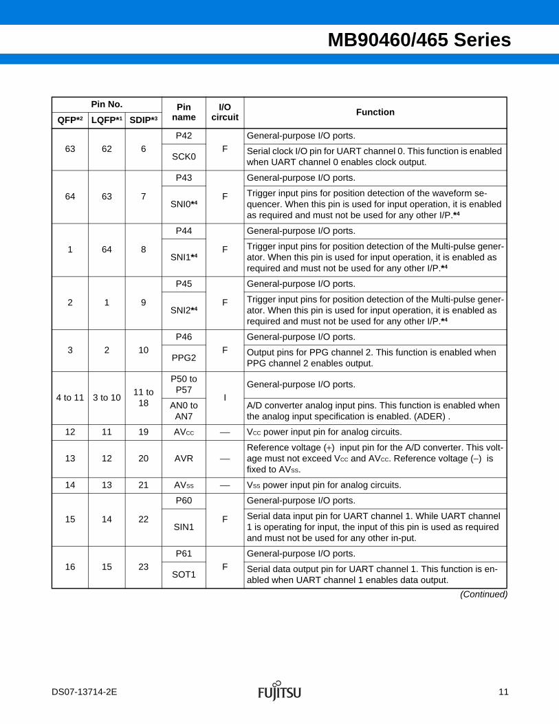
12 11 19 AVCC ⎯ VCC power input pin for analog circuits.
13 12 20 AVR ⎯Reference voltage (+) input pin for the A/D converter. This volt-age must not exceed VCC and AVCC. Reference voltage (−) is fixed to AVSS.
14 13 21 AVSS ⎯ VSS power input pin for analog circuits.
15 14 22
P60
F
General-purpose I/O ports.
SIN1Serial data input pin for UART channel 1. While UART channel 1 is operating for input, the input of this pin is used as required and must not be used for any other in-put.
16 15 23
P61
F
General-purpose I/O ports.
SOT1Serial data output pin for UART channel 1. This function is en-abled when UART channel 1 enables data output.
DS07-13714-2E 11

MB90460/465 Series
(Continued)
*1 : FPT-64P-M23
*2 : FPT-64P-M06
*3 : DIP-64P-M01
*4 : Pin names not applicable to MB90465 series
Pin No. Pin name
I/Ocircuit Function
QFP*2 LQFP*1 SDIP*3
17 16 24
P62
F
General-purpose I/O port.
SCK1Serial clock I/O pin for UART channel 1. This function is enabled when UART channel 1 enables clock output.
18 17 25
P63
F
General-purpose I/O port.
INT7Usable as interrupt request input channel 7. Input is enabled when 1 is set in EN7 in standby mode.
19 18 26 MD0 JInput pin for operation mode specification. Connect this pin di-rectly to VCC or VSS.
21, 22 20, 21 28, 29MD1, MD2
JInput pin for operation mode specification. Connect this pin di-rectly to VCC or VSS.
25, 50 24, 49 32, 57 VSS ⎯ Power (0 V) input pin.
57 56 64 VCC ⎯ Power (5 V) input pin.
58 57 1 C ⎯ Capacity pin for power stabilization. Please connect to an ap-proximately 0.1 µF ceramic capacitor.
12 DS07-13714-2E
MB90460/465 Series
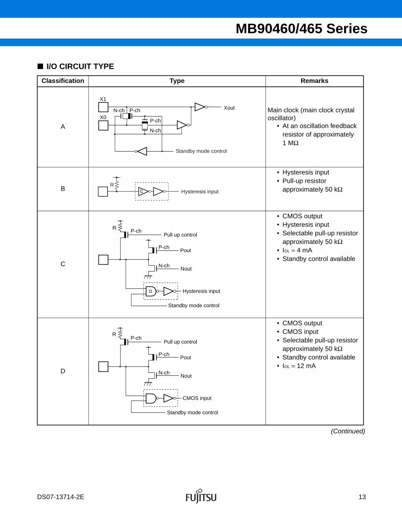
I/O CIRCUIT TYPE
(Continued)
Classification Type Remarks
A
Main clock (main clock crystal oscillator)
• At an oscillation feedback resistor of approximately1 MΩ
B
• Hysteresis input• Pull-up resistor
approximately 50 kΩ
C
• CMOS output• Hysteresis input• Selectable pull-up resistor
approximately 50 kΩ• IOL = 4 mA• Standby control available
D
• CMOS output• CMOS input• Selectable pull-up resistor
approximately 50 kΩ• Standby control available• IOL = 12 mA
X1
Xout
X0N-ch P-ch
N-ch
P-ch
Standby mode control
RHysteresis input
R
Pout
P-chPull up control
Hysteresis input
Standby mode control
P-ch
N-chNout
R
Pout
P-chPull up control
CMOS input
Standby mode control
P-ch
N-chNout
DS07-13714-2E 13

MB90460/465 Series
(Continued)
Classification Type Remarks
E
• CMOS output• CMOS input• Selectable pull-up resistor
approximately 50 kΩ• Standby control available• IOL = 4 mA
F
• CMOS output• Hysteresis input• Standby control available• IOL = 4 mA
G
• CMOS output• CMOS input• Standby control available• IOL = 12 mA
H
• CMOS output• CMOS input• Standby control available• IOL = 4 mA
R
Pout
P-chPull up control
CMOS input
Standby mode control
P-ch
N-chNout
Pout
Hysteresis input
Standby mode control
P-ch
N-chNout
Pout
CMOS input
Standby mode control
P-ch
N-chNout
Pout
CMOS input
Standby mode control
P-ch
N-chNout
14 DS07-13714-2E

MB90460/465 Series
(Continued)
Classification Type Remarks
I
• CMOS output• CMOS input• Analog input• IOL = 4 mA
J
• Hysteresis input
Pout
CMOS input
Analog input control
Analog input
P-ch
N-chNout
Hysteresis input
DS07-13714-2E 15

MB90460/465 Series
HANDLING DEVICES1. Preventing Latchup
CMOS ICs may cause latchup in the following situations : • When a voltage higher than VCC or lower than VSS is applied to input or output pins.• When a voltage exceeding the rating is applied between VCC and VSS.• When AVCC power is supplied prior to the VCC voltage.
If latchup occurs, the power supply current increases rapidly, sometimes resulting in thermal breakdown of thedevice. Use meticulous care not to let it occur.
For the same reason, also be careful not to let the analog power-supply voltage exceed the digital power-supplyvoltage.
2. Handling unused input pins
Unused input pins left open may cause abnormal operation, or latch-up leading to permanent damage. Unusedinput pins should be pulled up or pulled down through at least 2 kΩ resistance.
Unused input/output pins may be left open in the output state, but if such pins are in the input state they shouldbe handled in the same way as input pins.
3. Use of the external clock
When the device uses an external clock, drive only the X0 pin while leaving the X1 pin open (See the illustrationbelow) .
4. Power Supply Pins (VCC/VSS)
In products with multiple VCC or VSS pins, the pins of a same potential are internally connected in the device toavoid abnormal operations including latch-up. However, connect the pins external power and ground lines tolower the electro-magnetic emission level to prevent abnormal operation of strobe signals caused by the rise inthe ground level, and to conform to the total current rating.
Make sure to connect VCC and VSS pins via the lowest impedance to power lines.
It is recommended to provide a bypass capacitor of around 0.1 µF between VCC and VSS pins near the device.
5. Crystal Oscillator Circuit
Noise around X0 or X1 pins may cause abnormal operations. Make sure to provide bypass capacitors via theshortest distance from X0, X1 pins, crystal oscillator (or ceramic resonator) and ground lines, and make sure,to the utmost effort, that lines of oscillation circuit not cross the lines of other circuits.
It is highly recommended to provide a printed circuit board art work surrounding X0 and X1 pins with the groundarea for stabilizing the operation.
6. Turning-on Sequence of Power Supply to A/D Converter and Analog Inputs
Make sure to turn on the A/D converter power supply (AVCC, AVSS, AVR) and analog inputs (AN0 to AN7) afterturning-on the digital power supply (VCC) .
Turn-off the digital power after turning off the A/D converter supply and analog inputs. In this case, make surethat the voltage of AVR dose not exceed AVCC (turning on/off the analog and digital power supplies simultaneouslyis acceptable) .
X0
X1Open
MB90460/465 series
16 DS07-13714-2E
MB90460/465 Series
7. Connection of Unused Pins of A/D Converter
Connect unused pin of A/D converter to AVCC = VCC, AVSS = AVR = VSS.
8. N.C. Pin
The N.C. (internally connected) pin must be opened for use.
9. Notes on Energization
To prevent the internal regulator circuit from malfunctioning, set the voltage rise time during energization at 50µs or more.
10. Initialization
In the device, there are internal registers which are initialized only by a power-on reset. To initialize these registers,please turn on the power again.
11. Return from standby state
If the power-supply voltage goes below the standby RAM holding voltage in the standby state, the device mayfail to return from the standby state. In this case, reset the device via the external reset pin to return to the normalstate.
DS07-13714-2E 17
MB90460/465 Series
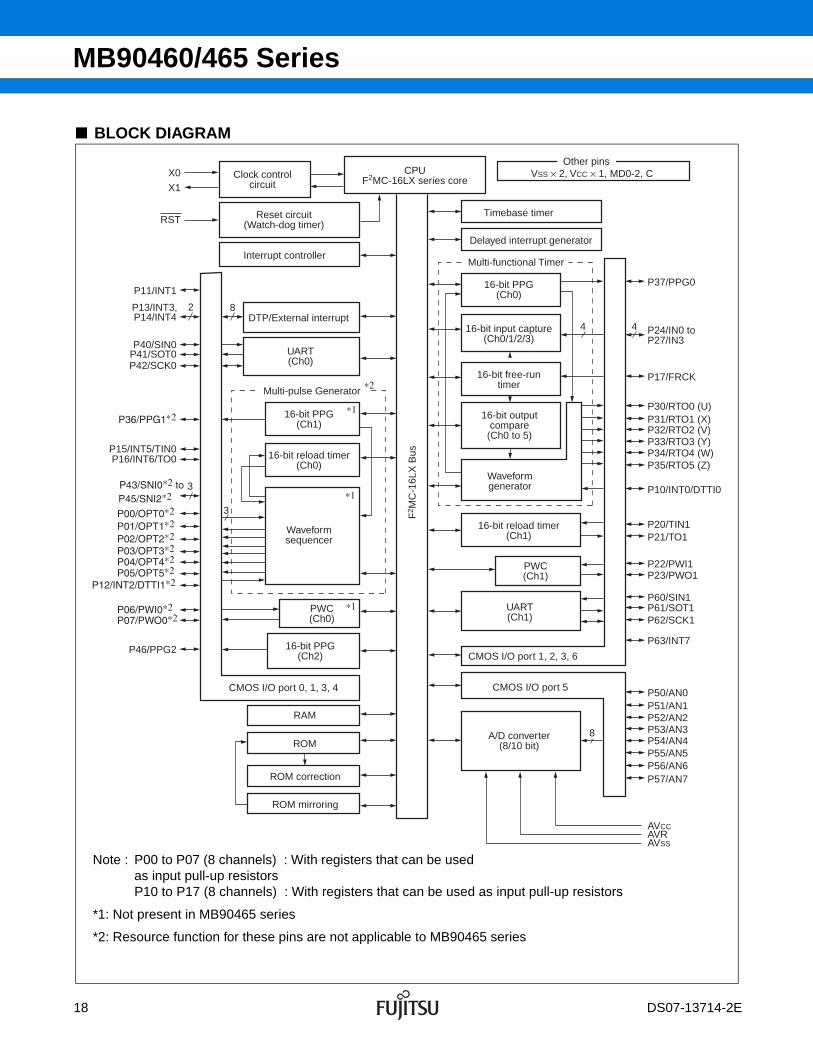
BLOCK DIAGRAM
X0
X1
RST
P11/INT1
P40/SIN0P41/SOT0P42/SCK0
P15/INT5/TIN0P16/INT6/TO0
P46/PPG2
P14/INT42
3
Clock controlcircuit
Reset circuit(Watch-dog timer)
Interrupt controller
DTP/External interrupt
UART(Ch0)
16-bit PPG(Ch1)
16-bit reload timer(Ch0)
Waveformsequencer
Multi-pulse Generator
3
8
PWC(Ch0)
16-bit PPG(Ch2)
CMOS I/O port 0, 1, 3, 4
RAM
ROM
ROM correction
ROM mirroring
F2 M
C-1
6LX
Bus
CPUF2MC-16LX series core
Other pinsVSS × 2, VCC × 1, MD0-2, C
Timebase timer
Delayed interrupt generator
Multi-functional Timer
4 4
16-bit PPG(Ch0)
16-bit input capture(Ch0/1/2/3)
16-bit free-runtimer
16-bit outputcompare
(Ch0 to 5)
Waveformgenerator
16-bit reload timer(Ch1)
PWC(Ch1)
UART(Ch1)
CMOS I/O port 1, 2, 3, 6
CMOS I/O port 5
A/D converter(8/10 bit)
P37/PPG0
P17/FRCK
P30/RTO0 (U)P31/RTO1 (X)P32/RTO2 (V)P33/RTO3 (Y)P34/RTO4 (W)P35/RTO5 (Z)
P10/INT0/DTTI0
P20/TIN1
P22/PWI1P23/PWO1
P60/SIN1P61/SOT1P62/SCK1
P63/INT7
P50/AN0P51/AN1P52/AN2P53/AN3P54/AN4P55/AN5P56/AN6P57/AN7
AVCCAVRAVSS
P21/TO1
P24/IN0 toP27/IN3
8
P13/INT3,
Note : P00 to P07 (8 channels) : With registers that can be used as input pull-up resistorsP10 to P17 (8 channels) : With registers that can be used as input pull-up resistors
*1: Not present in MB90465 series
*2: Resource function for these pins are not applicable to MB90465 series
18 DS07-13714-2E

MB90460/465 Series
MEMORY MAP
Note : The ROM data of bank FF is reflected in the upper address of bank 00, realizing effective use of the C compiler small model. The lower 16-bit is assigned to the same address, enabling reference of the table on the ROM without stating “far”. For example, if an attempt has been made to access 00C000H , the contents of the ROM at FFC000H are accessed actually. Since the ROM area of the FF bank exceeds 48 Kbytes, the whole area cannot be reflected in the image for the 00 bank. The ROM data at FF4000H to FFFFFFH looks, therefore, as if it were the image for 004000H to 00FFFFH. Thus, it is recommended that the ROM data table be stored in the area of FF4000H to FFFFFFH.
FFFFFFH
Address #1
Address #2
Address #3
FC0000H
010000H
004000H
003FE0H
000100H0000C0H
000000H
ROM area
Register
ROM area(FF bank image)
Peripheral area
Peripheral area
RAMarea
: Internal access memory
: Access not allowed
In Single chip modethe mirror functionis supported
Parts No. Address#1 Address#2 Address#3
MB90462/467 FF0000H 004000H 000900H
MB90F462 FF0000H 004000H 000900H
MB90F462A FF0000H 004000H 000900H
MB90F463A FE0000H 004000H 000900H
MB90V460 (FF0000H) 004000H 002100H
DS07-13714-2E 19

MB90460/465 Series
I/O MAP
(Continued)
Address Abbrevia-tion Register Byte
accessWord
accessResource
name Initial value
000000H PDR0 Port 0 data register R/W R/W Port 0 XXXXXXXXB
000001H PDR1 Port 1 data register R/W R/W Port 1 XXXXXXXXB
000002H PDR2 Port 2 data register R/W R/W Port 2 XXXXXXXXB
000003H PDR3 Port 3 data register R/W R/W Port 3 XXXXXXXXB
000004H PDR4 Port 4 data register R/W R/W Port 4 -XXXXXXXB
000005H PDR5 Port 5 data register R/W R/W Port 5 XXXXXXXXB
000006H PDR6 Port 6 data register R/W R/W Port 6 ----XXXXB
000007H Prohibited area
000008H PWCSL0PWC control status register CH0
R/W R/W
PWC timer* (CH0)
00000000B
000009H PWCSH0 R/W R/W 00000000B
00000AHPWC0 PWC data buffer register CH0 ⎯ R/W
XXXXXXXXB
00000BH XXXXXXXXB
00000CH DIV0 Divide ratio control register CH0 R/W R/W ------00B
00000DH to 0FH
Prohibited area
000010H DDR0 Port 0 direction register R/W R/W Port 0 00000000B
000011H DDR1 Port 1 direction register R/W R/W Port 1 00000000B
000012H DDR2 Port 2 direction register R/W R/W Port 2 00000000B
000013H DDR3 Port 3 direction register R/W R/W Port 3 00000000B
000014H DDR4 Port 4 direction register R/W R/W Port 4 -0000000B
000015H DDR5 Port 5 direction register R/W R/W Port 5 00000000B
000016H DDR6 Port 6 direction register R/W R/W Port 6 ----0000B
000017H ADER Analog input enable register R/W R/W Port 5, A/D 11111111B
000018H Prohibited area
000019H CDCR0 Clock division control register 0 R/W R/WCommunication
prescaler 00---0000B
00001AH Prohibited area
00001BH CDCR1 Clock division control register 1 R/W R/WCommunication
prescaler 10---0000B
00001CH RDR0 Port 0 pull-up resistor setting register R/W R/W Port 0 00000000B
00001DH RDR1 Port 1 pull-up resistor setting register R/W R/W Port 1 00000000B
00001EH to 1FH
Prohibited area
20 DS07-13714-2E

MB90460/465 Series
(Continued)
Address Abbrevia-tion Register Byte
accessWord
accessResource
name Initial value
000020H SMR0 Serial mode register 0 R/W R/W
UART0
00000000B
000021H SCR0 Serial control register 0 R/W R/W 00000100B
000022HSIDR0 / SODR0
Input data register 0 / output data register 0
R/W R/W XXXXXXXXB
000023H SSR0 Serial status register 0 R/W R/W 00001000B
000024H SMR1 Serial mode register 1 R/W R/W
UART1
00000000B
000025H SCR1 Serial control register 1 R/W R/W 00000100B
000026HSIDR1 / SODR1
Input data register 1 / output data register 1
R/W R/W XXXXXXXXB
000027H SSR1 Status register 1 R/W R/W 00001000B
000028H PWCSL1PWC control status register CH1
R/W R/W
PWC timer (CH1)
00000000B
000029H PWCSH1 R/W R/W 00000000B
00002AHPWC1 PWC data buffer register CH1 ⎯ R/W
XXXXXXXXB
00002BH XXXXXXXXB
00002CH DIV1 Divide ratio control register CH1 R/W R/W ------00B
00002DH to 2FH
Prohibited area
000030H ENIR Interrupt / DTP enable register R/W R/W
DTP/externalinterrupt
00000000B
000031H EIRR Interrupt / DTP cause register R/W R/W XXXXXXXXB
000032H ELVRLRequest level setting register (Lower Byte)
R/W R/W 00000000B
000033H ELVRHRequest level setting register (Higher Byte)
R/W R/W 00000000B
000034H ADCS0 A/D control status register 0 R/W R/W
8/10-bit A/Dconverter
00000000B
000035H ADCS1 A/D control status register 1 R/W R/W 00000000B
000036H ADCR0 A/D data register 0 R R XXXXXXXXB
000037H ADCR1 A/D data register 1 R/W R/W 00000-XXB
000038HPDCR0 PPG0 down counter register ⎯ R
16-bitPPG timer
(CH0)
11111111B
000039H 11111111B
00003AHPCSR0 PPG0 period setting register ⎯ W
XXXXXXXXB
00003BH XXXXXXXXB
00003CHPDUT0 PPG0 duty setting register ⎯ W
XXXXXXXXB
00003DH XXXXXXXXB
00003EH PCNTL0PPG0 control status register
R/W R/W --000000B
00003FH PCNTH0 R/W R/W 00000000B
DS07-13714-2E 21

MB90460/465 Series
(Continued)
Address Abbrevia-tion Register Byte
accessWord
accessResource
name Initial value
000040HPDCR1 PPG1 down counter register ⎯ R
16-bitPPG timer
(CH1) *
11111111B
000041H 11111111B
000042HPCSR1 PPG1 period setting register ⎯ W
XXXXXXXXB
000043H XXXXXXXXB
000044HPDUT1 PPG1 duty setting register ⎯ W
XXXXXXXXB
000045H XXXXXXXXB
000046H PCNTL1PPG1 control status register
R/W R/W --000000B
000047H PCNTH1 R/W R/W 00000000B
000048HPDCR2 PPG2 down counter register ⎯ R
16-bitPPG timer
(CH2)
11111111B
000049H 11111111B
00004AHPCSR2 PPG2 period setting register ⎯ W
XXXXXXXXB
00004BH XXXXXXXXB
00004CHPDUT2 PPG2 duty setting register ⎯ W
XXXXXXXXB
00004DH XXXXXXXXB
00004EH PCNTL2PPG2 control status register
R/W R/W --000000B
00004FH PCNTH2 R/W R/W 00000000B
000050HTMRR0 16-bit timer register 0 ⎯ R/W
Multi Function Timer (Wave-
form generator)
XXXXXXXXB
000051H XXXXXXXXB
000052HTMRR1 16-bit timer register 1 ⎯ R/W
XXXXXXXXB
000053H XXXXXXXXB
000054HTMRR2 16-bit timer register 2 ⎯ R/W
XXXXXXXXB
000055H XXXXXXXXB
000056H DTCR0 16-bit timer control register 0 R/W R/W 00000000B
000057H DTCR1 16-bit timer control register 1 R/W R/W 00000000B
000058H DTCR2 16-bit timer control register 2 R/W R/W 00000000B
000059H SIGCR Waveform control register R/W R/W 00000000B
00005AH CPCLRB /CPCLR
Compare clear buffer register /Compare clear register (lower)
⎯ R/W
16-bitfree-running
timer
11111111B
00005BH 11111111B
00005CHTCDT Timer data register (lower) ⎯ R/W
00000000B
00005DH 00000000B
00005EH TCCSL Timer control status register (lower) R/W R/W 00000000B
00005FH TCCSH Timer control status register (upper) R/W R/W -0000000B
22 DS07-13714-2E
MB90460/465 Series
(Continued)
Address Abbrevia-tion Register Byte
accessWord
accessResource
name Initial value
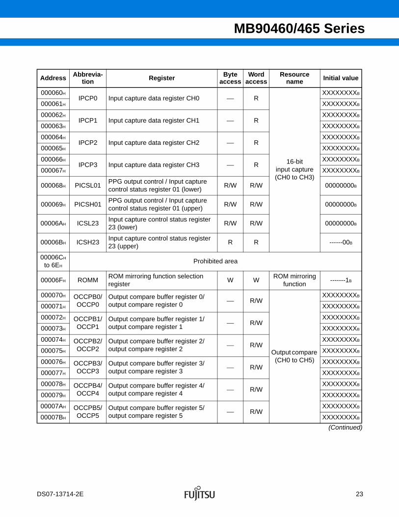
000060HIPCP0 Input capture data register CH0 ⎯ R
16-bitinput capture (CH0 to CH3)
XXXXXXXXB
000061H XXXXXXXXB
000062HIPCP1 Input capture data register CH1 ⎯ R
XXXXXXXXB
000063H XXXXXXXXB
000064HIPCP2 Input capture data register CH2 ⎯ R
XXXXXXXXB
000065H XXXXXXXXB
000066HIPCP3 Input capture data register CH3 ⎯ R
XXXXXXXXB
000067H XXXXXXXXB
000068H PICSL01PPG output control / Input capture control status register 01 (lower)
R/W R/W 00000000B
000069H PICSH01PPG output control / Input capture control status register 01 (upper)
R/W R/W 00000000B
00006AH ICSL23Input capture control status register 23 (lower)
R/W R/W 00000000B
00006BH ICSH23Input capture control status register 23 (upper)
R R ------00B
00006CH to 6EH
Prohibited area
00006FH ROMMROM mirroring function selection register
W WROM mirroring
function-------1B
000070H OCCPB0/OCCP0
Output compare buffer register 0/ output compare register 0
⎯ R/W
Output compare (CH0 to CH5)
XXXXXXXXB
000071H XXXXXXXXB
000072H OCCPB1/OCCP1
Output compare buffer register 1/ output compare register 1
⎯ R/WXXXXXXXXB
000073H XXXXXXXXB
000074H OCCPB2/OCCP2
Output compare buffer register 2/ output compare register 2
⎯ R/WXXXXXXXXB
000075H XXXXXXXXB
000076H OCCPB3/OCCP3
Output compare buffer register 3/ output compare register 3
⎯ R/WXXXXXXXXB
000077H XXXXXXXXB
000078H OCCPB4/OCCP4
Output compare buffer register 4/ output compare register 4
⎯ R/WXXXXXXXXB
000079H XXXXXXXXB
00007AH OCCPB5/OCCP5
Output compare buffer register 5/ output compare register 5
⎯ R/WXXXXXXXXB
00007BH XXXXXXXXB
DS07-13714-2E 23

MB90460/465 Series
(Continued)
Address Abbrevia-tion Register Byte
accessWord
accessResource
name Initial value
00007CH OCS0 Compare control register 0 R/W R/W
Output compare (CH0 to CH5)
00000000B
00007DH OCS1 Compare control register 1 R/W R/W -0000000B
00007EH OCS2 Compare control register 2 R/W R/W 00000000B
00007FH OCS3 Compare control register 3 R/W R/W -0000000B
000080H OCS4 Compare control register 4 R/W R/W 00000000B
000081H OCS5 Compare control register 5 R/W R/W -0000000B
000082H TMCSRL0Timer control status register CH0 (lower)
R/W R/W
16-bitreload timer
(CH0)
00000000B
000083H TMCSRH0Timer control status register CH0 (upper)
R/W R/W ----0000B
000084H TMR0 / TMRD0
16 bit timer register CH0 / 16-bit reload register CH0
⎯ R/WXXXXXXXXB
000085H XXXXXXXXB
000086H TMCSRL1Timer control status register CH1 (lower)
R/W R/W
16-bit reload timer (CH1)
00000000B
000087H TMCSRH1Timer control status register CH1 (upper)
R/W R/W ----0000B
000088H TMR1 / TMRD1
16 bit timer register CH1 / 16-bit reload register CH1
⎯ R/WXXXXXXXXB
000089H XXXXXXXXB
00008AH OPCLR Output control lower register R/W R/W
Waveform*sequencer
00000000B
00008BH OPCUR Output control upper register R/W R/W 00000000B
00008CH IPCLR Input control lower register R/W R/W 00000000B
00008DH IPCUR Input control upper register R/W R/W 00000000B
00008EH TCSR Timer control status register R/W R/W 00000000B
00008FH NCCR Noise cancellation control register R/W R/W 00000000B
000090H to 9DH
Prohibited area
00009EH PACSRProgram address detect control status register
R/W R/W Rom correction 00000000B
00009FH DIRRDelayed interrupt cause / clear register
R/W R/WDelayedinterrupt
-------0B
0000A0H LPMCRLow-power consumption mode register
R/W R/W Low-powerconsumption
control register
00011000B
0000A1H CKSCR Clock selection register R/W R/W 11111100B
0000A2H to A7H
Prohibited area
0000A8H WDTC Watchdog control register R/W R/W Watchdog timer X-XXX111B
0000A9H TBTC Timebase timer control register R/W R/W Timebase timer 1--00100B
24 DS07-13714-2E

MB90460/465 Series
(Continued)
Address Abbrevia-tion Register Byte
accessWord
accessResource
name Initial value
0000AAH to ADH
Prohibited area
0000AEH FMCSFlash memory control status register
R/W R/WFlash memory interface circuit
00010000B
0000AFH Prohibited area
0000B0H ICR00 Interrupt control register 00 R/W R/W
Interruptcontroller
00000111B
0000B1H ICR01 Interrupt control register 01 R/W R/W 00000111B
0000B2H ICR02 Interrupt control register 02 R/W R/W 00000111B
0000B3H ICR03 Interrupt control register 03 R/W R/W 00000111B
0000B4H ICR04 Interrupt control register 04 R/W R/W 00000111B
0000B5H ICR05 Interrupt control register 05 R/W R/W 00000111B
0000B6H ICR06 Interrupt control register 06 R/W R/W 00000111B
0000B7H ICR07 Interrupt control register 07 R/W R/W 00000111B
0000B8H ICR08 Interrupt control register 08 R/W R/W 00000111B
0000B9H ICR09 Interrupt control register 09 R/W R/W 00000111B
0000BAH ICR10 Interrupt control register 10 R/W R/W 00000111B
0000BBH ICR11 Interrupt control register 11 R/W R/W 00000111B
0000BCH ICR12 Interrupt control register 12 R/W R/W 00000111B
0000BDH ICR13 Interrupt control register 13 R/W R/W 00000111B
0000BEH ICR14 Interrupt control register 14 R/W R/W 00000111B
0000BFH ICR15 Interrupt control register 15 R/W R/W 00000111B
0000C0H to FFH
External area
001FF0H PADR0LProgram address detection register 0 (Lower Byte)
R/W R/W
Rom correction
XXXXXXXXB
001FF1H PADR0MProgram address detection register 0 (Middle Byte)
R/W R/W XXXXXXXXB
001FF2H PADR0HProgram address detection register 0 (Higher Byte)
R/W R/W XXXXXXXXB
001FF3H PADR1LProgram address detection register 1 (Lower Byte)
R/W R/W XXXXXXXXB
001FF4H PADR1MProgram address detection register 1 (Middle Byte)
R/W R/W XXXXXXXXB
001FF5H PADR1HProgram address detection register 1 (Higher Byte)
R/W R/W XXXXXXXXB
DS07-13714-2E 25

MB90460/465 Series
(Continued)
Address Abbrevia-tion Register Byte
accessWord
accessResource
name Initial value
003FE0HOPDBR0 Output data buffer register 0 ⎯ R/W
Waveform*sequencer
00000000B
003FE1H 00000000B
003FE2HOPDBR1 Output data buffer register 1 ⎯ R/W
00000000B
003FE3H 00000000B
003FE4HOPDBR2 Output data buffer register 2 ⎯ R/W
00000000B
003FE5H 00000000B
003FE6HOPDBR3 Output data buffer register 3 ⎯ R/W
00000000B
003FE7H 00000000B
003F78HOPDBR4 Output data buffer register 4 ⎯ R/W
00000000B
003FE9H 00000000B
003FEAHOPDBR5 Output data buffer register 5 ⎯ R/W
00000000B
003FEBH 00000000B
003FECHOPEBR6 Output data buffer register 6 ⎯ R/W
00000000B
003FEDH 00000000B
003FEEHOPEBR7 Output data buffer register 7 ⎯ R/W
00000000B
003FEFH 00000000B
003FF0HOPEBR8 Output data buffer register 8 ⎯ R/W
00000000B
003FF1H 00000000B
003FF2HOPEBR9 Output data buffer register 9 ⎯ R/W
00000000B
003FF3H 00000000B
003FF4HOPEBRA Output data buffer register A ⎯ R/W
00000000B
003FF5H 00000000B
003FF6HOPEBRB Output data buffer register B ⎯ R/W
00000000B
003FF7H 00000000B
003FF8HOPDR Output data register ⎯ R
XXXXXXXXB
003FF9H 0000XXXXB
003FFAHCPCR Compare clear register ⎯ R/W
XXXXXXXXB
003FFBH XXXXXXXXB
003FFCHTMBR Timer buffer register ⎯ R
00000000B
003FFDH 00000000B
003FFEH to
003FFFH
Prohibited area
26 DS07-13714-2E

MB90460/465 Series
• Meaning of abbreviations used for reading and writing
• Explanation of initial values
The Instruction using IO addressing e.g. MOV A, io, is not supported for registers area 003FE0H to 003FFFH.
Note : For bits that is initialized by an reset operation, the initial value set by the reset operation is listed as an initial value. Note that the values are different from reading results.For LPMCR/CKSCR/WDTC, there are cases where initialization is performed or not performed, depending on the types of the reset. However, initial value for resets that initializes the value is listed.
*: These registers are not present in MB90465 series
R/W : Read and write enabledR : Read onlyW : Write only
0 : The bit is initialized to 0.1 : The bit is initialized to 1.X : The initial value of the bit is undefined.- : The bit is not used. Its initial value is undefined.
DS07-13714-2E 27

MB90460/465 Series
INTERRUPT FACTORS, INTERRUPT VECTORS, INTERRUPT CONTROL REGISTER
(Continued)
Interrupt cause EI2OS support
Interrupt vector Interrupt control register Priority
*2
Number Address ICR Address
Reset #08 08H FFFFDCH ⎯ ⎯ High
INT9 instruction #09 09H FFFFD8H ⎯ ⎯
Exception processing #10 0AH FFFFD4H ⎯ ⎯
A/D converter conversion termination #11 0BH FFFFD0HICR00 0000B0H*1
Output compare channel 0 match #12 0CH FFFFCCH
End of measurement by PWC0 timer /PWC0 timer overflow*3 #13 0DH FFFFC8H
ICR01 0000B1H*1
16-bit PPG timer 0 #14 0EH FFFFC4H
Output compare channel 1 match3 #15 0FH FFFFC0HICR02 0000B2H*1
16-bit PPG timer 1*3 #16 10H FFFFBCH
Output compare channel 2 match #17 11H FFFFB8HICR03 0000B3H*1
16-bit reload timer 1 underflow #18 12H FFFFB4H
Output compare channel 3 match #19 13H FFFFB0H
ICR04 0000B4H*1DTP/ext. interrupt channels 0/1 detection#20 14H FFFFACH
DTTI0 ∆
Output compare channel 4 match #21 15H FFFFA8H
ICR05 0000B5H*2DTP/ext. interrupt channels 2/3 detection#22 16H FFFFA4H
DTTI1*3 ∆
Output compare channel 5 match #23 17H FFFFA0H
ICR06 0000B6H*1End of measurement by PWC1 timer /PWC1 timer overflow
#24 18H FFFF9CH
DTP/ext. interrupt channels 4/5 detection #25 19H FFFF98H
ICR07 0000B7H*1Waveform sequencer timer compare match / write timing*3 #26 1AH FFFF94H
DTP/ext. interrupt channels 6/7 detection #27 1BH FFFF90H
ICR08 0000B8H*1Waveform sequencer position detect /compare interrupt*3 #28 1CH FFFF8CH
Waveform generator 16-bit timer 0/1/2underflow
∆ #29 1DH FFFF88HICR09 0000B9H*1
16-bit reload timer 0 underflow #30 1EH FFFF84H
16-bit free-running timer zero detect ∆ #31 1FH FFFF80HICR10 0000BAH*1
16-bit PPG timer 2 #32 20H FFFF7CH
Input capture channels 0/1 #33 21H FFFF78HICR11 0000BBH*1
16-bit free-running timer compare clear ∆ #34 22H FFFF74H
×
×
×
28 DS07-13714-2E

MB90460/465 Series
(Continued)
: Can be used and support the EI2OS stop request. : Can be used and interrupt request flag is cleared by EI2OS interrupt clear signal. : Cannot be used.
∆ : Usable when an interrupt cause that shares the ICR is not used.
*1: - For peripheral functions that share the ICR register, the interrupt level will be the same. - If the extended intelligent I/O service is to be used with a peripheral function that shares the ICR register with
another peripheral function, the service can be started by either of the function. And if EI2OS clear is supported, both interrupt request flags for the two interrupt causes are cleared by EI2OS interrupt clear signal. It is recom-mended to mask either of the interrupt request during the use of EI2OS.
- EI2OS service cannot be started multiple times simultaneously. Interrupt other than the operating interrupt is masked during EI2OS operation. It is recommended to mask either of the interrupt requests during the use of EI2OS.
*2: This priority is applied when interrupts of the same level occur simultaneously.*3: In MB90465 series, these resources are not present, and therefore the interrupts are not available.
Interrupt cause EI2OS support
Interrupt vector Interrupt control register Priority
*2
Number Address ICR Address
Input capture channels 2/3 #35 23H FFFF70HICR12 0000BCH*1
Timebase timer ∆ #36 24H FFFF6CH
UART1 receive #37 25H FFFF68HICR13 0000BDH*1
UART1 send ∆ #38 26H FFFF64H
UART0 receive #39 27H FFFF60HICR14 0000BEH*1
UART0 send ∆ #40 28H FFFF5CH
Flash memory status ∆ #41 29H FFFF58HICR15 0000BFH*1
Delayed interrupt generator module ∆ #42 2AH FFFF54H Low
×
DS07-13714-2E 29

MB90460/465 Series
PERIPHERAL RESOURCES1. Low-Power Consumption Control Circuit
The MB90460/465 series has the following CPU operating mode configured by selection of an operating clockand clock operation control.• Clock mode
PLL clock mode : A PLL clock that is a multiple of the oscillation clock (HCLK) frequency is used to operatethe CPU and peripheral functions.Main clock mode : The main clock, with a frequency one-half that of the oscillation clock (HCLK) , is used tooperate the CPU and peripheral functions. In main clock mode, the PLL multiplier circuit is inactive.
• CPU intermittent operation modeCPU intermittent operation mode causes the CPU to operate intermittently, while high-speed clock pulses aresupplied to peripheral functions, reducing power consumption. In CPU intermittent operation mode, intermittentclock pulses are only applied to the CPU when it is accessing a register, internal memory, a peripheral function,or an external unit.
• Standby modeIn standby mode, the low power consumption control circuit stops supplying the clock to the CPU (sleep mode)or the CPU and peripheral functions (timebase timer mode) , or stops the oscillation clock itself (stop mode) , reducing power consumption.• PLL sleep mode
PLL sleep mode is activated to stop the CPU operating clock when the microcontroller enters PLL clockmode; other components continue to operate on the PLL clock.
• Main sleep modeMain sleep mode is activated to stop the CPU operating clock when the microcontroller enters main clockmode; other components continue to operate on the main clock.
• PLL timebase timer modePLL timebase timer mode causes microcontroller operation, with the exception of the oscillation clock, PLLclock and timebase timer, to stop. All functions other than the timebase timer are deactivated.
• Main timebase timer modeMain timebase timer mode causes microcontroller operation, with the exception of the oscillation clock, mainclock and the timebase timer, to stop. All functions other than the timebase timer are deactivated.
• Stop modeStop mode causes the source oscillation to stop. All functions are deactivated.
30 DS07-13714-2E

MB90460/465 Series
Block Diagram
RESV MCM WS1 WS0 RESV MCS CS1 CS0
STP
Pin
Pin
Pin
SLP SPL RST TMD CG1
CPU intermittentoperation selecter
Pin highimpedance
control circuit
Internal resetgeneration
circuit
CPU clockcontrol circuit
Peripheral clockcontrol circuit
CG0 RESV
2
2
X0
X1
RST
RSTRelease reset
Cancel interrupt
Clock generator
Low power mode control register (LPMCR)
Pin Hi-z control
Internal reset
CPU clock
Stop and sleep signals
Stop signal
Machine clock
Clock selector
Clock selection register (CKSCR)
Timebase timerSystem clockgeneration circuit
Oscillation stabilizationwait is passed
Peripheral clock
Oscillation stabilizationwait interval selector
Select intermittent cycles
Standby controlcircuit
PLL multipilercircuit
×1 ×2×3 ×4
Divide-by-4
Divide-by-4
Divide-by-4
Divide-by-2
Divide-by-512
Divide-by-2
Main clock
3
DS07-13714-2E 31

MB90460/465 Series
2. I/O Ports
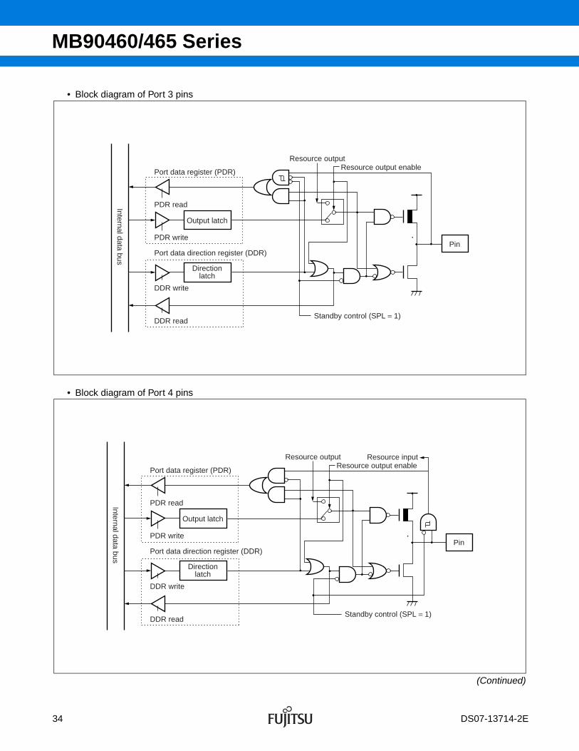
(1) Outline of I/O ports
When a data register serving for control output is read, the data output from it as a control output is read regardlessof the value in the direction register. Note that, if a read-modify-write instruction (such as a bit set instruction) isused to preset output data in the data register when changing its setting from input to output, the data read isnot the data register latched value but the input data from the pin.
Ports 0 to 4 and 6 are input/output ports which serve as inputs when the direction register value is “0” or asoutputs when the value is “1”.
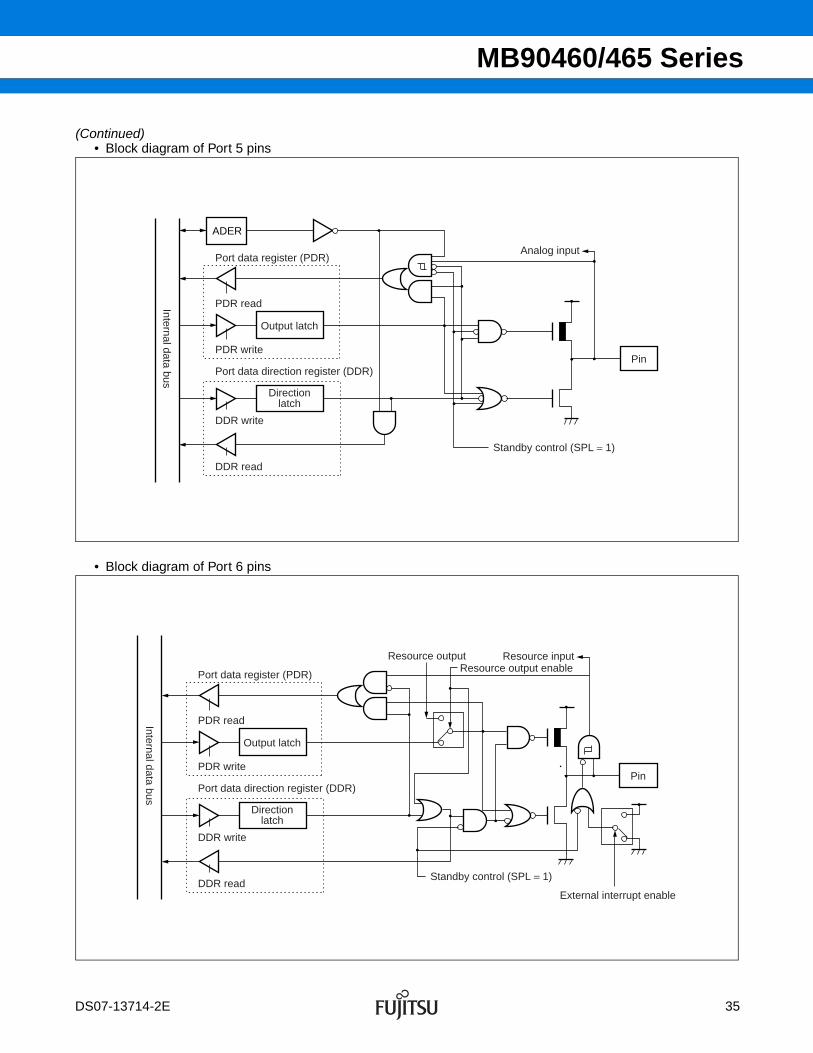
Port 5 are input/output ports as other port when ADER is 00H.
Block Diagram• Block diagram of Port 0 pins
(Continued)
RDR
Port data register (PDR)Resource output enable
Pull-up resistorAbout 50 KΩ
Standby control (SPL = 1)
PDR read
PDR write
DDR write
DDR read
Port data direction register (DDR)
Internal data bus
Output latch
Pin
Resource output
Directionlatch
Direct resource input
32 DS07-13714-2E

MB90460/465 Series
• Block diagram of Port 1 pins
• Block diagram of Port 2 pins
(Continued)
RDR
Port data register (PDR)Resource output enable
Pull-up resistorAbout 50 KΩ
Standby control (SPL = 1)
PDR read
PDR write
DDR write
DDR read
Port data direction register (DDR)
Internal data bus
Output latch
Pin
Resource output
Directionlatch
Resource input
Port data register (PDR)Resource output enable
Standby control (SPL = 1)
PDR read
PDR write
DDR write
DDR read
Port data direction register (DDR)
Internal data bus
Output latch
Pin
Resource output
Directionlatch
Resource input
DS07-13714-2E 33
MB90460/465 Series
• Block diagram of Port 3 pins
• Block diagram of Port 4 pins
(Continued)
Port data register (PDR)Resource output enable
Standby control (SPL = 1)
PDR read
PDR write
DDR write
DDR read
Port data direction register (DDR)
Internal data bus
Output latch
Pin
Resource output
Directionlatch
Port data register (PDR)Resource output enable
Standby control (SPL = 1)
PDR read
PDR write
DDR write
DDR read
Port data direction register (DDR)
Internal data bus
Output latch
Pin
Resource output
Directionlatch
Resource input
34 DS07-13714-2E
MB90460/465 Series
(Continued)• Block diagram of Port 5 pins
• Block diagram of Port 6 pins
ADER
Port data register (PDR)
Standby control (SPL = 1)
PDR read
PDR write
DDR write
DDR read
Port data direction register (DDR)
Internal data bus
Output latch
Pin
Directionlatch
Analog input
Port data register (PDR)Resource output enable
Standby control (SPL = 1)
PDR read
PDR write
DDR write
DDR read
Port data direction register (DDR)
Internal data bus
Output latch
Pin
Resource output
External interrupt enable
Directionlatch
Resource input
DS07-13714-2E 35

MB90460/465 Series
3. Timebase Timer
The timebase timer is an 18-bit free-running counter (timebase counter) that counts up in synchronization to theinternal count clock (main oscillator clock divided by 2) .
Features of timebase timer : • Interrupt generated when counter overflow• EI2OS supported• Interval timer function :
An interrupt generated at four different time intervals• Clock supply function :
Four different clocks can be selected as a watchdog timer’s count clockSupply clock for oscillation stabilization
Block Diagram
⎯ ⎯ ⎯ TBIE TBOF TBR TBC1 TBC0
× 21 × 22 × 23 × 28 × 29 × 210 × 211 × 212 × 213 × 214 × 215 × 216 × 218× 217
OF
Counterclear circuit
Intervaltimer selector
OF OF OF
Timebasetimer counter
Counter clear
Timebase timerinterrupt signal #36(24H)*2
TBOF clearTBOF set
Towatchdogtimer
To the oscillationsetting time selectorin the clock controlsection
Divide-by-two HCLK
Power-on reset
Stop mode start
CKSCR : MCS = 1 to 0 *1
Timebase timer interrptregister (TBTC)
OF : OverflowHCLK : Oscillation clock
*1 : Switching of the machine clock from the oscillation clock to the PLL clock
*2 : Interrupt number
36 DS07-13714-2E
MB90460/465 Series
4. Watchdog Timer
The watchdog timer is a 2-bit counter that uses the timebase timer’s supply clock as the count clock. Afteractivation, if the watchdog timer is not cleared within a given period, the CPU will be reset.• Features of Watchdog Timer :
Reset CPU at four different time intervalsStatus bits to indicate the reset causes
Block Diagram
PONR STBR WRST ERST SRST WTE WT1 WT0
× 21 × 22 × 28 × 29 × 210 × 211 × 212 × 213 × 214 × 215 × 216 × 217 × 218
2
4
Counterclear control
circuit
Countclock
selector
2-bitcounter
Watchdogreset generator
One-half of HCLK
Watchdog timer control register (WDTC)
Watchdog timer
Activationwith CLR
To theinternalresetgenerator
CLR
CLR
Clear
(Timebase timer counter)
Over-flow
Start of sleep mode
Start of hold status mode
Start of stop mode
HCLK : Oscillation clock
DS07-13714-2E 37

MB90460/465 Series
5. 16-bit reload timer ( × 2)
The 16-bit reload timer provides two operating mode, internal clock mode and event count mode. In eachoperating mode, the 16-bit down counter can be reloaded (reload mode) or stopped when underflow (one-shotmode) .
Output pins TO1 - TO0 are able to output different waveform accroding to the counter operating mode. TO1 -TO0 toggles when counter underflow if counter is operated as reload mode. TO1 - TO0 output specified level(H or L) when counter is counting if the counter is in one-shot mode.
Features of the 16 bit reload timer : • Interrupt generated when timer underflow• EI2OS supported• Internal clock operating mode :
Three internal count clocks can be selectedCounter can be activated by software or exteranl trigger (singal at TIN1 - TIN0 pin) Counter can be reloaded or stopped when underflow after activated
• Event count operating mode : Counter counts down by one when specified edge at TIN1 - TIN0 pinCounter can be reloaded or stopped when underflow
38 DS07-13714-2E
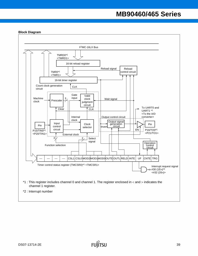
MB90460/465 Series
Block Diagram
TMRD0*1
<TMRD1>
Reload signal
Wait signal
Count clock generationcircuit
Machineclock
TMR0*1
<TMR1>
P15/TIN0*1
<P20/TIN1>
CLK
Gateinput
Clear
Internalclock
Selectsignal
EN
CLK
Invert
Output control circuit
To UART0 andUART1 *1
<To the A/Dconverter>
Interrupt request signal#30 (1EH)*2
<#32 (20H)>
P16/TO0*1
<P21/TO1>External clock
Function selection
Timer control status register (TMCSR0)*1 <TMCSR1>
3
3 2
⎯ ⎯ ⎯ ⎯ CSL1 CSL0 MOD2
F2MC-16LX Bus
16-bit reload register
16-bit timer register
Prescaler
Inputcontrolcircuit
Pin Pin
Validclock
judgmentcircuit
Clockselector
Output signalgeneration
circuit
Operationcontrolcircuit
Reloadcontrol circuit
MOD1MOD0OUTE OUTL RELD UFINTE CNTE TRG
*1 : This register includes channel 0 and channel 1. The register enclosed in < and > indicates the channel 1 register.
*2 : Interrupt number
DS07-13714-2E 39

MB90460/465 Series
6. 16-bit PPG Timer ( × 3, PPG1 is not present in MB90465 series)
The 16-bit PPG timer consists of a 16-bit down counter, prescaler, 16-bit period setting buffer register, 16-bitduty setting buffer register, 16-bit control register and a PPG output pin. This module can be used to outputpulses synchronized by software trigger or GATE signal from Multi-functional timer, refer to “Multi-functionalTimer”
Features of 16-bit PPG Timer : • Two operating mode : PWM and One-shot• 8 types of counter operation clock (φ, φ/2, φ/4, φ/8, φ/16, φ/32, φ/64, φ/128) can be selected• Interrupt generated when trigger signal arrived, or counter borrow, or change of PPG output• EI2OS supported
Block Diagram
Prescaler
CKS2 CKS1 CKS0
Period SettingBuffer Register 0/1/2
Duty SettingBuffer Register 0/1/2
Duty SettingRegister 0/1/2
Period SettingRegister 0/1/2
1/11/21/41/81/161/321/641/128
Machine clock φ
Dow
n C
ount
erR
egis
ter
0/1/
2
GATE-from multi-functionaltimer (for PPG ch. 0 only)
Edge detection
CLK LOAD
BORROWSTART
STOP
16-bitdown counter C
ompa
rato
r
S Q
R
MDSE PGMS OSEL POEN
Pin
P37/PPG0or
P36/PPG1or
P46/PPG2
PPG0 (multi-functional timer)or
PPG1 (multi-pulse generator)or
PPG2
Interruptselection Interrupt
#14/#16/#32
IRS1 IRS0 IRQFIREN
F2 M
C-1
6LX
Bus
(for PPG ch. 1 & 2)
STGR CNTE RTRG
40 DS07-13714-2E

MB90460/465 Series
7. Multi-functional Timer
The 16-bit multi-functional timer module consists of one 16-bit free-running timer, four input capture circuits, sixoutput comparators and one channel of 16-bit PPG timer. This module allows six independent waveformsgenerated by PPG timer or waveform generator to be outputted. With the 16-bit free-run timer and the inputcapture circuit, a input pulse width measurement and external clock cycle measurement can be done.
(1) 16-bit free-running timer (1 channel) • The 16-bit free-running timer consists of a 16-bit up/up-down counter, control register, 16-bit compare clear
register (with buffer register) and a prescaler.• 8 types of counter operation clock (φ, φ/2, φ/4, φ/8, φ/16, φ/32, φ/64, φ/128) can be selected. (φ is the machine
clock) • Two types of interrupt causes :
- Compare clear interrupt is generated when there is a comparing match with compare clear register and 16-bit free-run timer.- Zero detection interrupt is generated while 16-bit free-running timer is detected as zero in count value.
• EI2OS supported• The compare clear register has a selectable buffer register, into which data is written for transfer to the compare
clear register. When the timer is stopped, transfer occurs immediately when the data is written to the buffer.When the timer is operation, data transfer from the buffer occurs when the timer value is detected to be zero.
• Reset, software clear, compare match with compare clear register in up-count mode will reset the countervalue to “0000H”.
• Supply clock to output compare module : The prescaler ouptut is acted as the count clock of the output compare.
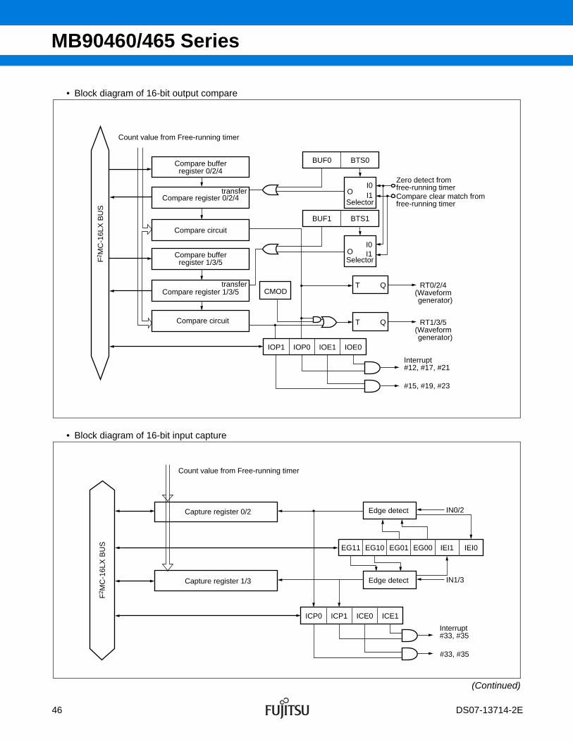
(2) Output compare module (6 channels) • The output compare module consists of six 16-bit compare registers (with selectable buffer register) , compare
output latch and compare control registers. An interrupt is generated and output level is inverted when thevalue of 16-bit free-running timer and compare register are matched.
• 6 compare registers can be operated independently.• Output pins and interrupt flag are corresponding to each compare register.• Inverts output pins by using 2 compare registers together. 2 compare registers can be paired to control the
output pins.• Setting the initial value for each output pin is possible.• Interrupt generated when there is a comparing match with output compare register and 16 bit free-run timer• EI2OS supported
(3) Input capture module (4 channels)
Input capture consists of 4 independent external input pins, the corresponding capture register and capturecontrol register. By detecting any edge of the input signal from the external pin, the value of the 16-bit free-running timer can be stored in the capture register and an interrupt is generated simultaneously.• Operation synchronized with the 16-bit free-run timer’s count clock.• 3 types of trigger edge (rising edge, falling edge and both edge) of the external input signal can be selected
and there is indication bit to show the trigger edge is rising or falling.• 4 input captures can be operated independently.• Two independent interrupts are generated when detecting a valid edge from external input.• EI2OS supported
(4) 16-bit PPG timer ( × 1)
The 16-bit PPG timer 0 is used to provide a PPG signal for waveform generator.
DS07-13714-2E 41
MB90460/465 Series
(5) Waveform Generator module
The waveform generator consists of three 16-bit timer registers, three timer control registers and 16-bit waveformcontrol register.
With waveform generator, it is possible to generate real time output, 16-bit PPG waveform output, non-overlap3-phase waveform output for inverter control and DC chopper waveform output.• It is possible to generate a non-overlap waveform output based on dead-time of 16-bit timer. (Dead-time timer
function) • It is possible to generate a non-overlap waveform output when realtime output is operated in 2-channel mode.
(Dead-time timer function) • By detecting realtime output compare match, GATE signal of the PPG timer operation will be generated to
start or stop PPG timer operation. (GATE function) • When a match is detected by realtime output compare, the 16-bit timer is activated. The PPG timer can be
started or stopped easily by generating a GATE signal for PPG operation until the 16-bit timer stops. (GATEfunction)
• Forced to stop output waveform using DTTI0 pin input• Interrupt generated when DTTI0 active or 16-bit tmer underflow• EI2OS supported
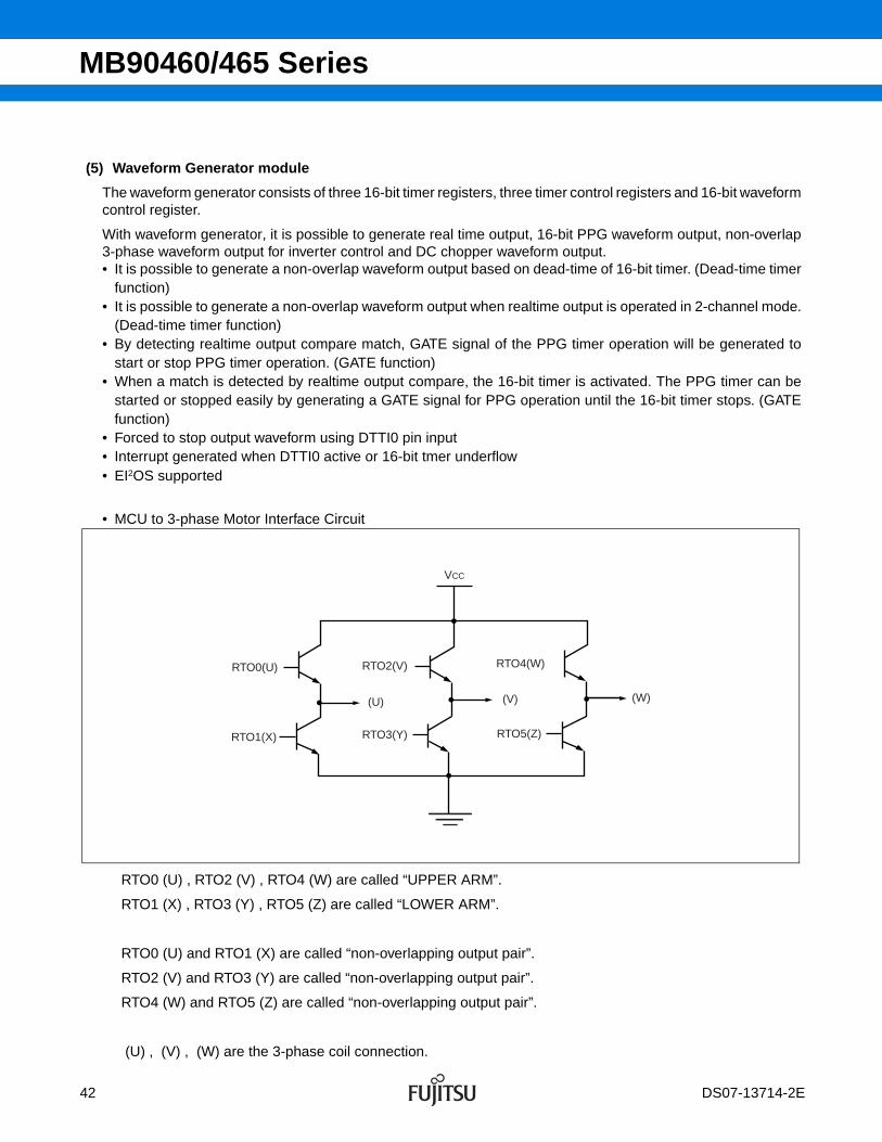
• MCU to 3-phase Motor Interface Circuit
RTO0 (U) , RTO2 (V) , RTO4 (W) are called “UPPER ARM”.
RTO1 (X) , RTO3 (Y) , RTO5 (Z) are called “LOWER ARM”.
RTO0 (U) and RTO1 (X) are called “non-overlapping output pair”.
RTO2 (V) and RTO3 (Y) are called “non-overlapping output pair”.
RTO4 (W) and RTO5 (Z) are called “non-overlapping output pair”.
(U) , (V) , (W) are the 3-phase coil connection.
RTO4(W)
(V)
RTO5(Z)
(W)
RTO2(V)
(U)
RTO3(Y)
RTO0(U)
RTO1(X)
VCC
42 DS07-13714-2E
MB90460/465 Series
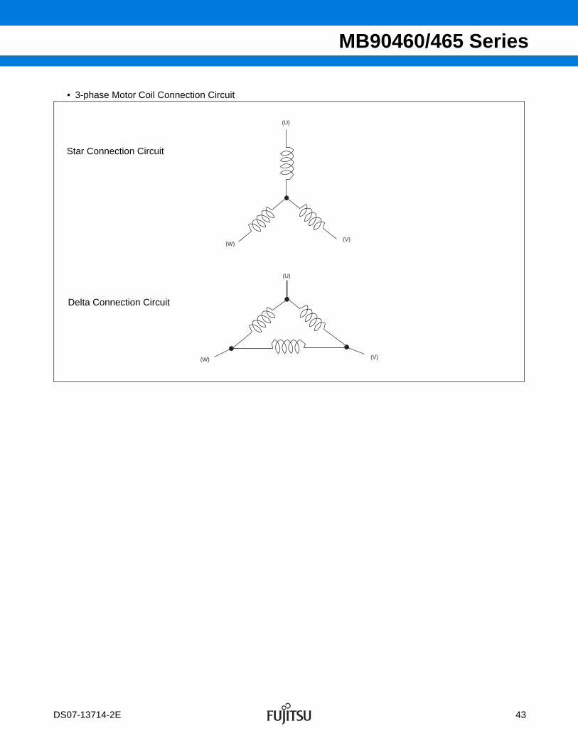
• 3-phase Motor Coil Connection Circuit
(U)
(V)(W)
(V)(W)
(U)
Star Connection Circuit
Delta Connection Circuit
DS07-13714-2E 43

MB90460/465 Series
Block Diagram• Block Diagram of Multi-functional Timer
(Continued)
Real time I/O
Interrupt#12Interrupt#15Interrupt#17Interrupt#19Interrupt#21Interrupt#23
output compare 0output compare 1output compare 2output compare 3output compare 4output compare 5
RT0 to 5
16-bit OutputCompare
buffertransfer
countervalue
16-bit free-running
timer
Interrupt#31Interrupt#34
A/D trigger A/D trigger
EXCK
Zero detectCompare clear
Input capture 0/1Input capture 2/3
countervalue Interrupt #33
Interrupt #35
16-bit InputCapture
IN0
IN1
IN2
IN3
RT0 to 5
Waveformgenerator
RTO0
RTO1
RTO2
RTO3
RTO4
RTO5
DTTI
PPG0 PPG0
GATE GATE
Interrupt#29 16-bit timer 0/1/2underflow
Interrupt#20 DTTI0 falling edge detect
Pin
Pin
Pin
Pin
Pin
Pin
Pin
Pin
Pin
Pin
Pin
Pin
P24/IN0
P17/FRCK
P10/INT0/DTTI0
P35/RTO5 (Z)
P34/RTO4 (W)
P33/RTO3 (Y)
P32/RTO2 (V)
P31/RTO1 (X)
P30/RTO0 (U)
P25/IN1
P26/IN2
P27/IN3
F2 M
C-1
6LX
Bus
44 DS07-13714-2E
MB90460/465 Series
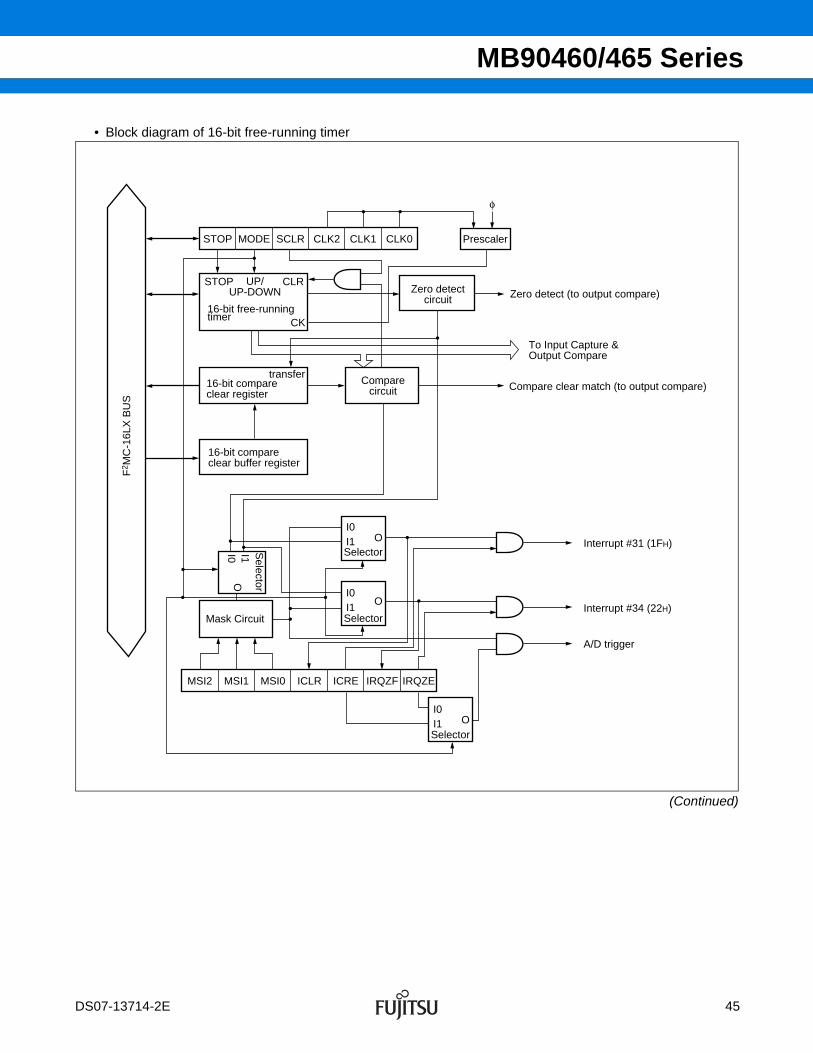
• Block diagram of 16-bit free-running timer
(Continued)
F2 M
C-1
6LX
BU
S
φ
PrescalerSTOP MODE SCLR CLK2 CLK1 CLK0
Zero detectcircuit Zero detect (to output compare)
STOP UP/UP-DOWN
CLR
16-bit free-runningtimer CK
transfer16-bit compareclear register
Comparecircuit
To Input Capture &Output Compare
Compare clear match (to output compare)
16-bit compareclear buffer register
Selector
I0 I1O
Mask Circuit Selector
Selector
I0I1
I0I1
O
O
Selector
I0I1 O
MSI2 MSI1 MSI0 ICLR ICRE IRQZF IRQZE
A/D trigger
Interrupt #34 (22H)
Interrupt #31 (1FH)
DS07-13714-2E 45
MB90460/465 Series
• Block diagram of 16-bit output compare
• Block diagram of 16-bit input capture
(Continued)
BUF0
BUF1
BTS0
BTS1
Selector
Selector
O
O
I0I1
I0I1
Zero detect fromfree-running timerCompare clear match fromfree-running timer
Count value from Free-running timer
Compare bufferregister 0/2/4
Compare register 0/2/4
Compare register 1/3/5
Compare circuit
Compare circuit
Compare bufferregister 1/3/5
transfer
transfer
CMOD
F2 M
C-1
6LX
BU
S
T Q
T Q RT0/2/4(Waveform generator)
RT1/3/5(Waveform generator)
IOP1 IOP0 IOE1 IOE0
Interrupt#12, #17, #21
#15, #19, #23
Count value from Free-running timer
Capture register 0/2
Capture register 1/3
F2 M
C-1
6LX
BU
S
Interrupt#33, #35
#33, #35
IN0/2
IN1/3
Edge detect
Edge detect
EG11 EG10 EG01 EG00 IEI1 IEI0
ICP0 ICP1 ICE0 ICE1
46 DS07-13714-2E

MB90460/465 Series
(Continued)• Block diagram of waveform generator
F2 M
C-1
6LX
BU
S
φ
Divider
DCK2 DCK1 DCK0 NRSL DTIF DTIE NWS1 NWS0 SIGCR
DTTI0Noise CancellationDTTI0 control circuit
GATE 0/1
GATE(to PPG0)TO0
TO1
TO2
TO3
TO4
TO5
U
X
V
Y
W
Z
Waveform control
Selector
Out
put C
ontr
olO
utpu
t Con
trol
Out
put C
ontr
ol
RTO0 (U)
RTO1 (X)
RTO2 (V)
RTO3 (Y)
RTO4 (W)
RTO5 (Z)
Selector
Selector
Selector
GATE 4/5
GATE 2/3
Dead time generator
Dead time generator
Dead time generator
Selector
Selector
Waveform control
Waveform control
PICSH01
DTCR0
RT0
RT1
RT2
RT3
RT4
RT5
16-bit timer 0
16-bit timer register 0
16-bit timer register 1
16-bit timer register 2
Compare circuit
16-bit timer 1 Compare circuit
16-bit timer 2 Compare circuit
DTCR1
DTCR2
PICSH01
PICSH01
PP
G0
TMD2 TMD1 TMD0 GTEN1 GTEN0
TMD2 TMD1 TMD0 GTEN1 GTEN0
TMD2 TMD1 TMD0 GTEN1 GTEN0
PGEN5 PGEN4
PGEN3 PGEN2
PGEN1 PGEN0
DS07-13714-2E 47

MB90460/465 Series
8. Multi-Pulse Generator (Not present in MB90465 series, but the 16-bit reload timer 0 can be used individually)
The Multi-pulse Generator consists of a 16-bit PPG timer, a 16-bit reload timer and a waveform sequencer. Byusing the waveform sequencer, 16-bit PPG timer output signal can be directed to Multi-pulse Generator output(OPT5 to 0) according to the input signal of Multi-pulse Generator (SNI2 to 0) . Meanwhile, the OPT5 to 0 outputsignal can be hardware terminated by DTTI input (DTTI1) in case of emergency. The OPT5 to 0 output signalsare synchronized with the PPG signal in order to eliminate the unwanted glitch.
The Multi-pulse generator has the following features : • Output Signal Control
- 12 output data buffer registers are provided- Output data register can be updated by any one of output data buffer registers when : 1. an effective edge detected at SNI2 - SNI0 pin2. 16-bit reload timer underflow3. output data buffer register OPDBR0 is written
• Output data register (OPDR) determines which OPT terminals (OPT5 - 0) output the 16-bit PPG waveform- Waveform sequencer is provided with a 16-bit timer to measure the speed of motor- The 16-bit timer can be used to disable the OPT output when the position detection is missing
• Input Position Detect Control- SNI2 - SNI0 input can be used to detect the rotor position- A controllable noise filter is provided to the SNI2 - SNI0 input
• PPG Synchronization for Output signal- OPT output is able to synchronize the edge of PPG waveform to avoid a short pulse (or glitch) appearance
• Vaious interrupt generation causes• EI2OS supported
(1) 16-bit PPG timer (x 1, not present in MB90465 series)
The 16-bit PPG timer 1 is used to provide a PPG signal for waveform sequencer.
(2) 16-bit reload timer (x 1)
The 16-bit reload timer 0 is used to provide signal to waveform sequencer.
(3) Waveform sequencer (not present in MB90465 series)
By using the waveform sequencer, 16-bit PPG timer output signal can be directed to Multi-pulse generator output(OPT5 ~ OPT0) according to the input signal of Multi-pulse generator (SNI2 ~ SNI0). Meanwhile, the OPT5 ~OPT0 outputsignal can be hardware terminated by DTTI input (DTTI1) in case of emergency. The OPT5 ~ OPT0output signalsare synchronized with the PPG signal in order to eliminate the unwanted glitch.
48 DS07-13714-2E

MB90460/465 Series
Block Diagram• Block diagram of Multi-pulse generator
(Continued)
F2 M
C-1
6LX
Bus
16-BIT PPG TIMER 1
16-BIT RELOAD TIMER 0TOUT
TIN
PPG1
DTTI
SNI2
SNI1
SNI0
TIN0
Pin
Pin
Pin
Pin
Pin
P12/INT2/DTTI1
P15/INT5/TIN0
P45/SNI2
P44/SNI1
P43/SNI0
PPG1
WIN0
TIN0O
WAVEFORMSEQUENCER
OPT5
OPT4
OPT3
OPT2
OPT1
OPT0
Pin
Pin
Pin
Pin
Pin
Pin
Pin
P05/OPT5
P04/OPT4
P03/OPT3
P02/OPT2
P01/OPT1
P00/OPT0
P16/INT6/TO0
INTERRUPT #22
INTERRUPT #26
INTERRUPT #28
Interrupt #22
Interrupt #26
Interrupt #28
Pin P15/INT5/TIN0
*
* : The dash line is the TIN0 path for MB90465 series. The 16-bit reload timer 0 can be used individually in MB90465 series.
DS07-13714-2E 49

MB90460/465 Series
(Continued)• Block diagram of waveform sequencer
Interrupt #22WRITE TIMING INTERRUPT
OPCR Register
POSITION DETECTION INTERRUPT
Interrupt#26
PDIRT
From PPG1WTS1WTS0
SYN Circuit
Pin
Pin
Pin
Pin
Pin
Pin
P00/OPT0
P01/OPT1
P02/OPT2
P03/OPT3
P04/OPT4
P05/OPT5
P12/INT2/DTTI1
Pin
D1D0
NoiseFilter
DTTI1 ControlCircuit
OUTPUTCONTROLCIRCUIT
DTIE DTIF NRSL OPS2 OPS1 OPS0 WTIF WTIE PDIF PDIE OPE5 OPE4 OPE3 OPE2 OPE1 OPE0
OP
DB
RB
to 0
Reg
iste
rs
OU
TP
UT
DA
TA
BU
FF
ER
RE
GIS
TE
R ×
12
DE
CO
DE
R
OP
DR
Reg
iste
r
OP
× 1
/OP
× 0
RD
A2
to 0
BN
KF
3 3
COMPARE CLEAR INTERRUPT
F2 M
C-1
6LX
Bus
16-BIT TIMERWTO
WTIN1CCIRT
Pin P15/INT5/TIN0
P43/SNI0
P44/SNI1
P45/SNI2
Pin
Pin
Pin
POSITIONDETECTCIRCUIT
WTIN1WTIN1
3OPS2OPS1OPS0
TIN0O
DATA WRITECONTROL UNIT
SELECTOR
TIN0O WTIN0
WTIN0
WTO
COMPARISON CIRCUIT
IPCR Register
NCCR Register
WTS1 WTS0 CPIF CPIE CPD2 CPD1 CPD0 CMPE CPE1 CPE0 SNC2 SNC1 SNC0 SEE2 SEE1 SEE0
PDIRT Interrupt #28
COMPARE MATCH INTERRUPT
D0D1S00S01S10S11S20S21
50 DS07-13714-2E
MB90460/465 Series
9. PWC Timer (x 2, PWC0 is not present in MB90465 series)
The PWC (pulse width count) timer is a 16-bit multi-function up-counter with reload timer functions and input-signal pulse-width count functions as well.
The PWC timer consists of a 16-bit counter, on input pulse divider, a divide ratio control register, a count inputpin, a pulse output pin, and a 16-bit control register.
The PWC timer has the following features : • Interrupt generated when timer overflow or end of PWC measurement.• EI2OS supported• Timer functions :
- Generates an interrupt request at set time intervals.- Outputs pulse signals synchronized with the timer cycle.- Selects the counter clock from among three internal clocks.
• Pulse-width count functions- Counts the time between external pulse input events.- Selects the counter clock from among three internal clocks.- Count mode• H pulse width (rising edge to falling edge) /L pulse width (falling edge to rising edge) • Rising-edge cycle (rising edge to falling edge) /Falling-edge cycle (falling edge to rising edge) • Count between edges (rising or falling edge to falling or rising edge) Capable of counting cycles by dividing input pulses by 22, 24, 26, 28 using an 8-bit input divider.Generates an interrupt request upon the completion of count operation.Selects single or consecutive count operation.
DS07-13714-2E 51

MB90460/465 Series
Block Diagram
ERRPWC read
PWC
Reload
Overflow
Data transfer
16
16
16
Errordetection
16
16-bit up count timer
Control circuit
Clock
F.F.
Clockdivider
Edgedetection
F2 M
C-1
6LX
bus
Writ
e en
able
d
15
ERRCKS0CKS1
PWCS
DIVR
8-bitdivider
2
22
23
P06/PWI0P22/PWI1
P07/PWO0P23/PWO1
Divisionrateselection
Start edgeselectionCount endedge
End edgeselection
Cou
nt b
itou
tput
Fla
g se
tting
Divider ON/OFF
Overflow
Timer clearCountenabled
Count start edge
Count end interrupt request
Overflow interrupt request
CKS1, CKS0,Divider clear
Internal clock(machine clock / 4)
52 DS07-13714-2E
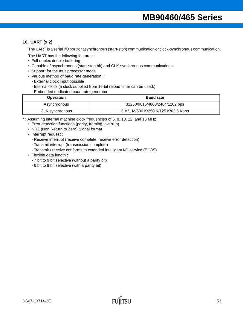
MB90460/465 Series
10. UART (x 2)
The UART is a serial I/O port for asynchronous (start-stop) communication or clock-synchronous communication.
The UART has the following features : • Full-duplex double buffering• Capable of asynchronous (start-stop bit) and CLK-synchronous communications• Support for the multiprocessor mode• Various method of baud rate generation :
- External clock input possible- Internal clock (a clock supplied from 16-bit reload timer can be used.) - Embedded dedicated baud rate generator
* : Assuming internal machine clock frequencies of 6, 8, 10, 12, and 16 MHz• Error detection functions (parity, framing, overrun) • NRZ (Non Return to Zero) Signal format• Interrupt request :
- Receive interrupt (receive complete, receive error detection) - Transmit interrupt (transmission complete) - Transmit / receive conforms to extended intelligent I/O service (EI2OS)
• Flexible data length : - 7 bit to 9 bit selective (without a parity bit) - 6 bit to 8 bit selective (with a parity bit)
Operation Baud rate
Asynchronous 31250/9615/4808/2404/1202 bps
CLK synchronous 2 M/1 M/500 K/250 K/125 K/62.5 Kbps
DS07-13714-2E 53

MB90460/465 Series
Block Diagram
PEOREFRERDRFTDREBDSRIETIE
MD1MD0CS2CS1CS0RSTSCKESOE
PENPSBLCLA/DRECRXETXE
MD
DIV2DIV1DIV0
SOT0, 1
SCK0, 1
SIN0, 1
Clockselector
Receptioncontrolcircuit
Reception clock
Reception bitcounter
Reception paritycounter
Start bit detection circuit
Send clock
send controlcircuit
Send start circuit
Send bit counter
Send parity counter
Reception interruptrequest output
Send interrupt request output
End
of r
ecep
tion
Sta
rt o
f tra
nsm
issi
on
Reception shift register
Send shift register
Reception statusdetermination circuit
16-bit reload timer
Dedicated baudrate generator
Control bus
Pin
Pin
Pin
Serial inputdata register (0, 1)
Serial outputdata register (0, 1)
receive error generation signal(to CPU)
2EI OS
Internal data bus
Serialstatusregister0, 1
Serial controlregister0, 1
Serialmoderegister0, 1
Communicationprescalercontrolregister
54 DS07-13714-2E

MB90460/465 Series
11. DTP/External Interrupts
The DTP/external interrupt circuit is activated by the signal supplied to a DTP/external interrupt pin. The CPUaccepts the signal using the same procedure it uses for normal hardware interrupts and generates externalinterrupts or activates the extended intelligent I/O service (EI2OS) .
Features of DTP/External Interrupt : • Total 8 external interrupt channels• Two request levels (“H” and “L”) are provided for the intelligent I/O service.• Four request levels (rising edge, falling edge, “H” level and “L” level) are provided for external interrupt requests.
Block Diagram
LB7
ER7 ER6 ER5 ER4 ER3 ER2 ER1 ER0
EN7 EN6 EN5 EN4 EN3 EN2 EN1 EN0
P63/INT7 P10/INT0/DTTI0
LA7 LB6 LA6 LB5 LA5 LB4 LA4 LB3 LA3 LB2 LA2 LB1 LA1 LB0 LA0
P16/INT6/TO0 P11/INT1
P12/INT2/DTTI1
P13/INT3
P15/INT5/TIN0
P14/INT4
Pin Pin
Pin Pin
Pin
Pin
Selector
Selector
Selector
Selector
Pin
Pin
Internal data bus
Selector
Selector
Selector
Selector
#20(14H)
Interrupt request number
Request level setting register (ELVR)
#22(16H)
#25(19H)
#27(1BH)
2 2 2 2 2 2 2 2
DS07-13714-2E 55

MB90460/465 Series
12. Delayed Interrupt Generation Module
The delayed interrupt generation module is used to generate a task switching interrupt. Interrupt requests to theF2MC-16LX CPU can be generated and cleared by software using this module.
Block Diagram
Delayed interrupt cause issuance/cancellation decoder
Interrupt cause latchF2 M
C-
16LX
bus
56 DS07-13714-2E

MB90460/465 Series
13. A/D Converter
The converter converts the analog voltage input to an analog input pin (input voltage) to a digital value. Theconverter has the following features : • The minimum conversion time is 6.13 µs (for a machine clock of 16 MHz; includes the sampling time) .• The minimum sampling time is 2.0 µs (for a machine clock of 16 MHz) .• The converter uses the RC-type successive approximation conversion method with a sample hold circuit.• A resolution of 10 bits or 8 bits can be selected.• Up to eight channels for analog input pins can be selected by a program.• Various conversion mode :
- Single conversion mode : Selectively convert one channel.- Scan conversion mode : Continuously convert multiple channels. Maximum of 8 program selectable channels.- Continuous conversion mode : Repeatedly convert specified channels.- Stop conversion mode : Convert one channel then halt until the next activation. (Enables synchronization ofthe conversion start timing.)
• At the end of A/D conversion, an interrupt request can be generated and EI2OS can be activated.• In the interrupt-enabled state, the conversion data protection function prevents any part of the data from being
lost through continuous conversion.• The conversion can be activated by software, 16-bit reload timer 1 (rising edge) and 16-bit free-running timer
zero detection edge.
DS07-13714-2E 57

MB90460/465 Series
Block Diagram
MPX
AVSSAVR
D/A converter
AVCC
AN0AN1AN2AN3AN4AN5AN6AN7
ADCS0/1
ADCR0/1
16-bit reload timer 1
16-bit free-running timer zero detection
φ
Sequential compare register
Data register
ComparatorInpu
t circ
uit
Sample and hold circuit
Prescaler
A/D control register 0
A/D control register 1
Operation clock
F2 M
C-1
6LX
bus
Dec
oder
φ : Machine clock
58 DS07-13714-2E

MB90460/465 Series
14. ROM Correction Function
In the case that the address of the instruction after the one that a program is currently processing matches theaddress configured in the detection address configuration register, the program forces the next instruction to beprocessed into an INT9 instruction, and branches to the interrupt process program. Since processing can beconducted using INT9 interrupts, programs can be repaired using batch processing.
•Overview of the Rom correction Function• The address of the instruction after the one that a program is currently processing is always stored in an
address latch via the internal data bus. Address match detection constantly compares the address stored inthe address latch with the one configured in the detection address configuration register. If the two comparedaddresses match, the CPU forcibly changes this instruction into an INT9 instruction, and executes an interruptprocessing program.
• There are two detection address configuration registers : PADR0 and PADR1. Each register provides aninterrupt enable bit. This allows you to individually configure each register to enable/prohibit the generation ofinterrupts when the address stored in the address latch matches the one configured in the detection addressconfiguration register.
Block Diagram
• Address latchStores value of address output to internal data bus.
• Address detection control register (PACSR) Set this register to enable/prohibit interrupt output when an address match is detected.
• Detection address configuration register (PADR0, PADR1) Configure an address with which to compare the address latch value.
PACSR
PADR0 (24 bit)
PADR1 (24 bit)
Address latch
Detection address configuration register 0
Detection address configuration register 1
Com
para
tor INT9 instruction
(INT9 interrupt generation)
Re-served
Re-served
Re-servedAD0ERe-
servedAD1ERe-served
Re-served
Inte
rnal
dat
a bu
s
Address detection control register (PACSR)
Reserved : Make sure this is always set to “01”
DS07-13714-2E 59

MB90460/465 Series
15. ROM Mirroring Function Selection Module
The ROM mirroring function selection module can select what the FF bank allocated the ROM and see throughthe 00 bank according to register settings.
Block Diagram
ROM
ROM mirroring register
Address area
FF bank 00 bank
F2 M
C-1
6LX
bus
60 DS07-13714-2E

MB90460/465 Series
16. 512/1024 Kbit Flash Memory
The 512 Kbit (MB90F462 and MB90F462A) or 1024 Kbit (MB90F463A) flash memory is allocated in the FEHtoFFH banks on the CPU memory map. Like masked ROM, flash memory is read-accessible and program-accessible to the CPU using the flash memory interface circuit.
The flash memory can be programmed/erased by the instruction from the CPU via the flash memory interfacecircuit. The flash memory can therefore be reprogrammed (updated) while still on the circuit board under inte-grated CPU control, allowing program code and data to be improved efficiently.
Note that sector operations such as “enable sector protect” cannot be used.
Features of 512/1024 Kbit flash memory• 64K words x 8 bits/32K words x 16 bits (16K+8K+8K+32K) sector configuration for MB90F462/F462A• 128K words x 8 bits/64K words x 16 bits (64K+16K+8K+8K+32K) sector configuration for MB90F463A• 64 kwords × 8 bits/32 kwords × 16 bits (16 k + 8 k + 8 k + 32 k) sector configuration• Automatic program algorithm (same as the Embedded Algorithm : MBM29F400TA) • Installation of the deletion temporary stop/delete restart function• Write/delete completion detected by the data polling or toggle bit• Write/delete completion detected by the CPU interrupt• Compatibility with the JEDEC standard-type command• Each sector deletion can be executed (Sectors can be freely combined) .• Flash security feature• Number of write/delete operations 10,000 times guaranteed.• Flash reading cycle time (Min) 2 machine cycles
DS07-13714-2E 61

MB90460/465 Series
(1) Sector configuration of 512Kbit flash memory
The flash memory has the sector configuration illustrated below. The addresses in the illustration are the upperand lower addresses of each sector.
When 512 Kbit flash memory is accessed from the CPU, SA0 to SA3 are allocated in the FF bank registers,respectively.
When 1024 Kbit flash memory is accessed from the CPU, SA0 and SA1 to SA4 are allocated in the FE andFFbank registers, respectively.
FFFFFFH
FFC000H
FFBFFFH
FFA000H
FF9FFFH
FF8000H
FF7FFFH
FF0000H
7FFFFH
7C000H
7BFFFH
7A000H
79FFFH
78000H
77FFFH
70000H
SA3 (16 Kbytes)
SA2 (8 Kbytes)
SA1 (8 Kbytes)
SA0 (32 Kbytes)
Flash memory CPU address *Writer address
FFFFFFH
FFC000H
FFBFFFH
FFA000H
FF9FFFH
FF8000H
FF7FFFH
FF0000H
7FFFFH
7C000H
7BFFFH
7A000H
79FFFH
78000H
77FFFH
70000H
SA4 (16 Kbytes)
SA3 (8 Kbytes)
SA2 (8 Kbytes)
SA1 (32 Kbytes)
Flash memory CPU address *Writer address
FEFFFFH
FE0000H
6FFFFH
60000H
SA0 (64 Kbytes)
62 DS07-13714-2E
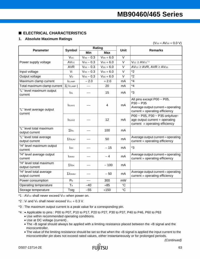
MB90460/465 Series
ELECTRICAL CHARACTERISTICS1. Absolute Maximum Ratings
(VSS = AVSS = 0.0 V)
*1 : AVCC shall never exceed VCC when power on.
*2 : VI and VO shall never exceed VCC + 0.3 V.
*3 : The maximum output current is a peak value for a corresponding pin.
*4 : • Applicable to pins : P00 to P07, P10 to P17, P20 to P27, P30 to P37, P40 to P46, P60 to P63• Use within recommended operating conditions.• Use at DC voltage (current) .• The +B signal should always be applied with a limiting resistance placed between the +B signal and the
microcontroller.• The value of the limiting resistance should be set so that when the +B signal is applied the input current to the
microcontroller pin does not exceed rated values, either instantaneously or for prolonged periods.(Continued)
Parameter SymbolRating
Unit RemarksMin Max
Power supply voltage
VCC VSS − 0.3 VSS + 6.0 V
AVCC VSS − 0.3 VSS + 6.0 V VCC ≥ AVCC* 1
AVR VSS − 0.3 VSS + 6.0 V AVCC ≥ AVR, AVR ≥ AVSS
Input voltage VI VSS − 0.3 VSS + 6.0 V *2
Output voltage VO VSS − 0.3 VSS + 6.0 V *2
Maximum clamp current ICLAMP − 2.0 + 2.0 mA *4
Total maximum clamp current Σ| ICLAMP | ⎯ 20 mA *4
“L” level maximum output current
IOL ⎯ 15 mA *3
“L” level average output current
IOLAV1 ⎯ 4 mA
All pins except P00 ~ P05, P30 ~ P35Average output current = operating current × operating efficiency
IOLAV2 ⎯ 12 mAP00 ~ P05, P30 ~ P35 onlyAver-age output current = operating current × operating efficiency
“L” level total maximum output current
ΣIOL ⎯ 100 mA
“L” level total average output current
Σ IOLAV ⎯ 50 mAAverage output current = operating current × operating efficiency
“H” level maximum output current
IOH ⎯ − 15 mA *3
“H” level average outputcurrent
IOHAV ⎯ − 4 mAAverage output current = operating current × operating efficiency
“H” level total maximum output current
ΣIOH ⎯ − 100 mA
“H” level total average output current
ΣIOHAV ⎯ − 50 mAAverage output current = operating current × operating efficiency
Power consumption PD ⎯ 300 mW
Operating temperature TA −40 +85 °CStorage temperature Tstg −55 +150 °C
DS07-13714-2E 63
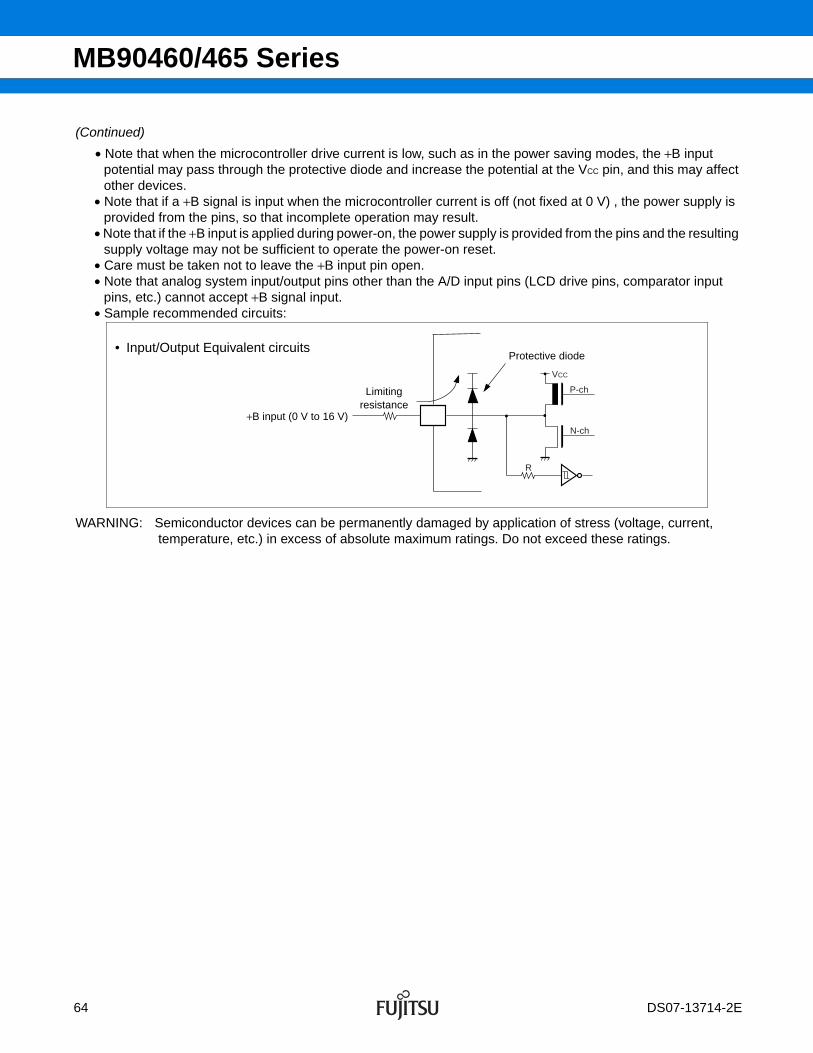
MB90460/465 Series
(Continued)
• Note that when the microcontroller drive current is low, such as in the power saving modes, the +B inputpotential may pass through the protective diode and increase the potential at the VCC pin, and this may affectother devices.
• Note that if a +B signal is input when the microcontroller current is off (not fixed at 0 V) , the power supply isprovided from the pins, so that incomplete operation may result.
• Note that if the +B input is applied during power-on, the power supply is provided from the pins and the resultingsupply voltage may not be sufficient to operate the power-on reset.
• Care must be taken not to leave the +B input pin open.• Note that analog system input/output pins other than the A/D input pins (LCD drive pins, comparator input
pins, etc.) cannot accept +B signal input.• Sample recommended circuits:
WARNING: Semiconductor devices can be permanently damaged by application of stress (voltage, current, temperature, etc.) in excess of absolute maximum ratings. Do not exceed these ratings.
P-ch
N-ch
VCC
R
• Input/Output Equivalent circuits
+B input (0 V to 16 V)
Limitingresistance
Protective diode
64 DS07-13714-2E

MB90460/465 Series
2. Recommended Operating Conditions (VSS = AVSS = 0.0 V)
WARNING: The recommended operating conditions are required in order to ensure the normal operation of the semiconductor device. All of the device's electrical characteristics are warranted when the device is operated within these ranges.
Always use semiconductor devices within their recommended operating condition ranges. Operation outside these ranges may adversely affect reliability and could result in device failure.No warranty is made with respect to uses, operating conditions, or combinations not represented on the data sheet. Users considering application outside the listed conditions are advised to contact their representatives beforehand.
Parameter Sym-bol
ValueUnit Remarks
Min Max
Power supply voltage
VCC
3.0 5.5 V Normal operation (MB90462, MB90467, MB90V460)
4.5 5.5 VNormal operation (MB90F462, MB90F462A, MB90F463A)
VCC 3.0 5.5 V Retains status at the time of operation stop
Smoothingcapacitor
CS 0.1 1.0 µF
Use a ceramic capacitor or a capacitor with equiva-lent frequency characteristics. The smoothing capac-itor to be connected to the VCC pin must have a capacitance value higher than CS.
Operating temperature
TA −40 +85 °C
C
CS
• C pin connection circuit
DS07-13714-2E 65

MB90460/465 Series
3. DC Characteristics (VCC = 5.0 V ± 10%, VSS = AVSS = 0.0 V, TA = −40 °C to +85 °C)
(Continued)
Parameter Sym-bol Pin name Condition
ValueUnit Remarks
Min Typ Max
“H” level output voltage
VOH All output pinsVCC = 4.5 V, IOH = − 4.0 mA
VCC − 0.5 ⎯ ⎯ V
“L” level output voltage
VOL
All pins except P00 to P05 and P30 to P35
VCC = 4.5 V, IOL = 4.0 mA
⎯ ⎯ 0.4 V
P00 to P05, P30 to P35
VCC = 4.5 V, IOL = 12.0 mA
⎯ ⎯ 0.4 V
“H” level input voltage
VIH
P00 to P07P30 to P37P50 to P57
VCC = 3.0 V to 5.5 V (MB90462, MB90467)
VCC = 4.5 V to 5.5 V (MB90F463, MB90F462A, MB90F463A)
0.7 VCC ⎯ VCC + 0.3 VCMOS input pin
VIHS
P10 to P17P20 to P27P40 to P46P60 to P63, RST
0.8 VCC ⎯ VCC + 0.3 VCMOS hyster-esis input pin
VIHM MD0 to MD2 VCC − 0.3 ⎯ VCC + 0.3 V MD pin input
“L” level input voltage
VIL
P00 to P07P30 to P37P50 to P57
VSS − 0.3 ⎯ 0.3 VCC VCMOS input pin
VILS
P10 to P17P20 to P27P40 to P46P60 to P63, RST
VSS − 0.3 ⎯ 0.2 VCC VCMOS hyster-esis input pin
VILM MD0 to MD2 VSS − 0.3 ⎯ VSS + 0.3 V MD pin input
Input leakage current
IIL All input pinsVCC = 5.5 V, VSS < VI < VCC
− 5 ⎯ 5 µA
66 DS07-13714-2E

MB90460/465 Series
(Continued) (VCC = 5.0 V ± 10%, VSS = AVSS = 0.0 V, TA = −40 °C to +85 °C)
* : The current value is preliminary value and may be subject to change for enhanced characteristics without previous notice. The power supply current is measured with an external clock.
Parameter Sym-bol Pin name Condition
ValueUnit Remarks
Min Typ Max
Power supply current*
ICC
VCC
VCC = 5.0 V, Internal opera-tion at 16 MHz, Normal operation
⎯ 40 50 mAMB90462, MB90467
⎯ 30 50 mAMB90F462, MB90F462A, MB90F463A
VCC = 5.0 V, Internal opera-tion at 16 MHz, When data writ-ten in flash mode programming of erasing
⎯ 45 60 mAMB90F462, MB90F462A, MB90F463A
ICCS
VCC = 5.0 V, Internal opera-tion at 16 MHz, In sleep mode
⎯ 15 20 mA
MB90462, MB90467,MB90F462, MB90F462A, MB90F463A
ICTS
VCC = 5.0 V, Internal opera-tion at 16 MHz, In Timer mode, TA = 25 °C
⎯ 2.5 5.0 mA
MB90462, MB90467,MB90F462, MB90F462A, MB90F463A
ICCHIn stop mode, TA = 25 °C ⎯ 5 20 µA
MB90462, MB90467,MB90F462, MB90F462A, MB90F463A
Input capacitance
CIN
Except AVCC, AVSS, C, VCC and VSS
⎯ ⎯ 10 80 pF
Pull-up resistance
RUP
P00 to P07 P10 to P17 RST
⎯ 25 50 100 kΩ
Pull-down resistance
RDOWN MD2 ⎯ 25 50 100 kΩ
DS07-13714-2E 67

MB90460/465 Series
4. AC Characteristics
(1) Clock Timings (VCC = 5.0 V ± 10%, VSS = AVSS = 0.0 V, TA = −40 °C to +85 °C)
*1 : The frequency fluctuation rate is the maximum deviation rate of the preset center frequency when the multiplied PLL signal is locked.
*2 : Internal operating clock frequency must not be over 16 MHz.
Parameter Symbol Pin name
ValueUnit Remarks
Min Typ Max
Clock frequency fC X0, X13 ⎯ 16
MHzCrystal oscillator
3 ⎯ 32 External clock *2
Clock cycle time tHCYL X0, X162.5 ⎯ 333 ns Crystal oscillator
31.25 ⎯ 333 ns External clock
Frequency fluctuation rate locked*1 ∆f ⎯ ⎯ ⎯ 5 %
Input clock pulse width PWH PWL X0 10 ⎯ ⎯ nsRecommened duty ratio of 30% to 70%
Input clock rise/fall timetCR
tCFX0 ⎯ ⎯ 5 ns External clock operation
Internal operating clock fCP ⎯ 1.5 ⎯ 16 MHz Main clock operation
Internal operating clock cycle time
tCP ⎯ 62.5 ⎯ 666 ns Main clock operation
+α⎥ α ⎥
fofo
−α
∆f = × 100 (%)Center
frequency
0.8 VCC
0.2 VCC
tCF tCR
tHCYL
PWH PWL
X0
68 DS07-13714-2E

MB90460/465 Series
The AC ratings are measured for the following measurement reference voltages
Relationship between internal operating clock frequency and power supply voltage
Relationship between oscillating frequency and internal operating clock frequency
5.5
4.5
3.03.3
8
Internal clock fCP (MHz)
Pow
er s
uppl
y vo
ltage
VC
C (
V)
1 3 12 16
Operation guarantee range of MB90F462MB90F462A, MB90F463A
Operation guarantee range of PLLOperation guarantee rangeof MB90462, MB90467, MB90V460
16
12
89
4
3 4 8
Oscillation clock fC (MHz)
Inte
rnal
clo
ck fC
P (
MH
z)
16
Multiplied-by-4
Multiplied-by-3
Multiplied-by-2
Multiplied-by-1
Not multiplied
0.8 VCC
0.2 VCC
2.4 V
0.8 V
0.7 VCC
0.3 VCC
• Input signal waveform
Hysteresis Input Pin
Pin other than hysteresis input/MD input
• Output signal waveform
Output Pin
DS07-13714-2E 69

MB90460/465 Series
(2) Reset Input Timing (VCC = 5.0 V ± 10%, VSS = AVSS = 0.0 V, TA = −40 °C to +85 °C)
* : Oscillation time of oscillator is time that amplitude reached the 90%. In the crystal oscillator, the oscillation time is between several ms to tens of ms. In ceramic oscillator, the oscillation time is between handreds µs to several ms. In the external clock, the oscillation time is 0 ms.
Parameter Symbol Pin ConditionValue
Units RemarksMin Max
Reset input time tRSTL RST ⎯4 tCP ⎯ ns Under normal operation
Oscillation time of oscillator + 4 tCP* ⎯ ms In stop mode
tRSTL
0.2 VCC 0.2 VCC
4 tCP
RST
X0
Internal operation clock
Internal reset
90% ofamplitude
Oscillation time ofoscillator Oscillation setting time
Instruction execution
• In stop mode
70 DS07-13714-2E
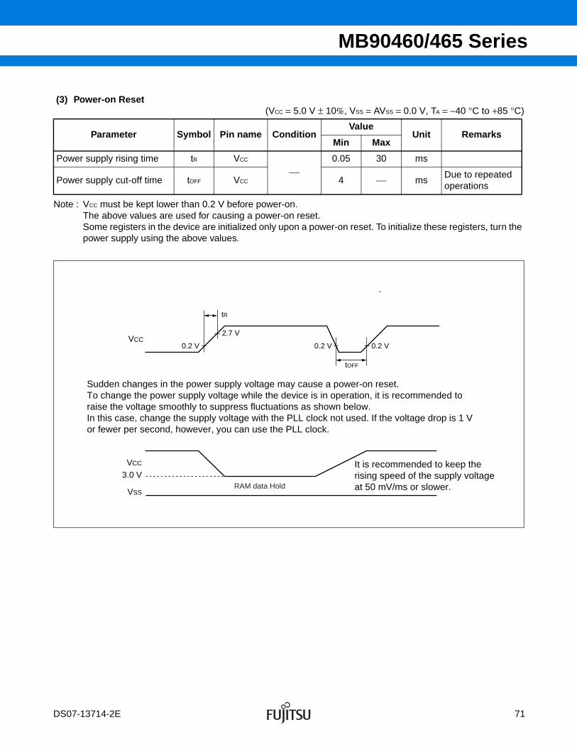
MB90460/465 Series
(3) Power-on Reset (VCC = 5.0 V ± 10%, VSS = AVSS = 0.0 V, TA = −40 °C to +85 °C)
Note : VCC must be kept lower than 0.2 V before power-on.The above values are used for causing a power-on reset. Some registers in the device are initialized only upon a power-on reset. To initialize these registers, turn the power supply using the above values.
Parameter Symbol Pin name ConditionValue
Unit RemarksMin Max
Power supply rising time tR VCC
⎯0.05 30 ms
Power supply cut-off time tOFF VCC 4 ⎯ msDue to repeated operations
VCC
VCC
VSS
3.0 V
tR
tOFF
2.7 V
0.2 V 0.2 V0.2 V
RAM data Hold
Sudden changes in the power supply voltage may cause a power-on reset.To change the power supply voltage while the device is in operation, it is recommended to raise the voltage smoothly to suppress fluctuations as shown below.In this case, change the supply voltage with the PLL clock not used. If the voltage drop is 1 V or fewer per second, however, you can use the PLL clock.
It is recommended to keep the rising speed of the supply voltage at 50 mV/ms or slower.
DS07-13714-2E 71
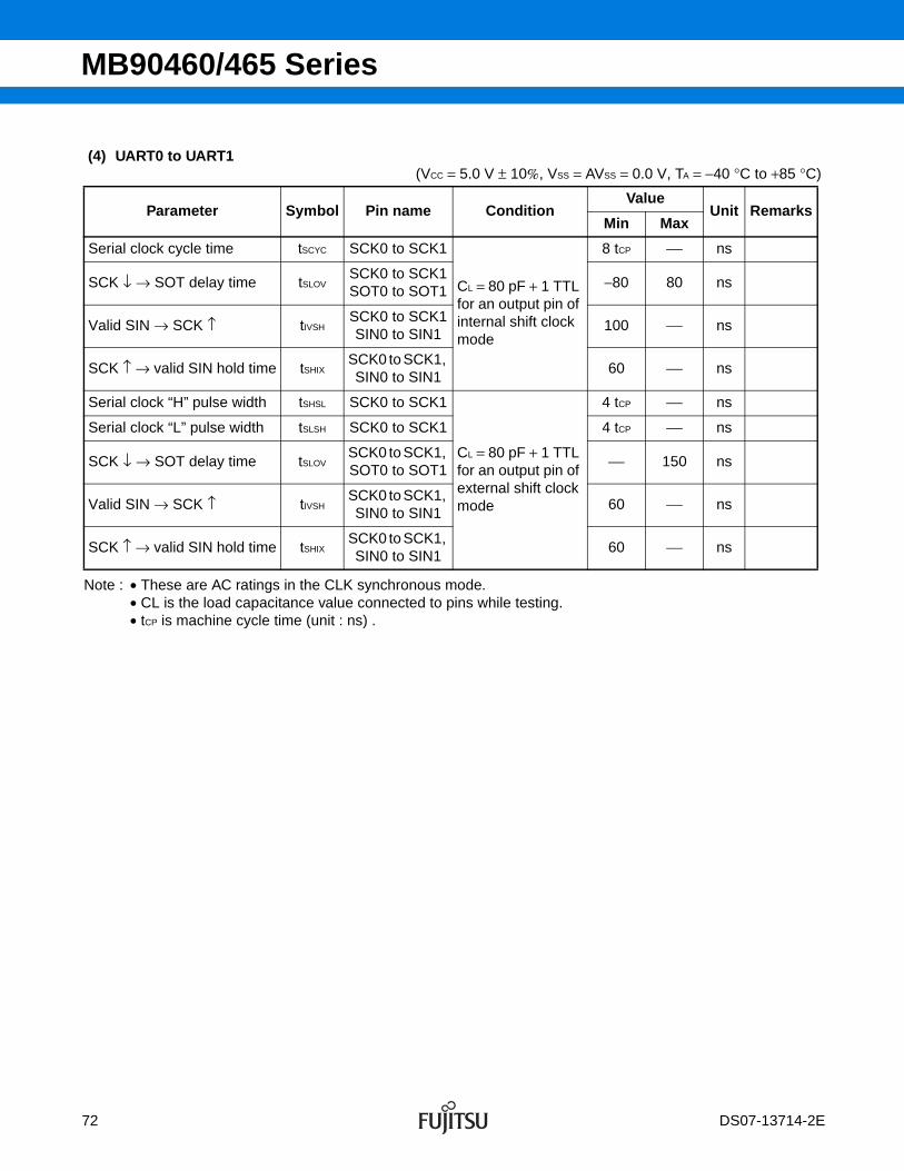
MB90460/465 Series
(4) UART0 to UART1 (VCC = 5.0 V ± 10%, VSS = AVSS = 0.0 V, TA = −40 °C to +85 °C)
Note : • These are AC ratings in the CLK synchronous mode.• CL is the load capacitance value connected to pins while testing.• tCP is machine cycle time (unit : ns) .
Parameter Symbol Pin name ConditionValue
Unit RemarksMin Max
Serial clock cycle time tSCYC SCK0 to SCK1
CL = 80 pF + 1 TTL for an output pin of internal shift clock mode
8 tCP ⎯ ns
SCK ↓ → SOT delay time tSLOVSCK0 to SCK1SOT0 to SOT1
−80 80 ns
Valid SIN → SCK ↑ tIVSHSCK0 to SCK1SIN0 to SIN1
100 ⎯ ns
SCK ↑ → valid SIN hold time tSHIXSCK0 to SCK1, SIN0 to SIN1
60 ⎯ ns
Serial clock “H” pulse width tSHSL SCK0 to SCK1
CL = 80 pF + 1 TTL for an output pin of external shift clock mode
4 tCP ⎯ ns
Serial clock “L” pulse width tSLSH SCK0 to SCK1 4 tCP ⎯ ns
SCK ↓ → SOT delay time tSLOVSCK0 to SCK1, SOT0 to SOT1
⎯ 150 ns
Valid SIN → SCK ↑ tIVSHSCK0 to SCK1, SIN0 to SIN1
60 ⎯ ns
SCK ↑ → valid SIN hold time tSHIXSCK0 to SCK1, SIN0 to SIN1
60 ⎯ ns
72 DS07-13714-2E

MB90460/465 Series
• Internal shift clock mode
• External shift clock mode
SCK
SOT
SIN
tSCYC
tSLOV
tIVSH tSHIX
0.8 V 0.8 V
2.4 V
2.4 V
0.8 V
0.8 VCC
0.2 VCC
0.8 VCC
0.2 VCC
SCK
SOT
SIN
tSLSH tSHSL
tSLOV
tIVSH tSHIX
0.2 VCC 0.2 VCC
0.8 VCC 0.8 VCC
2.4 V
0.8 V
0.8 VCC
0.2 VCC
0.8 VCC
0.2 VCC
DS07-13714-2E 73
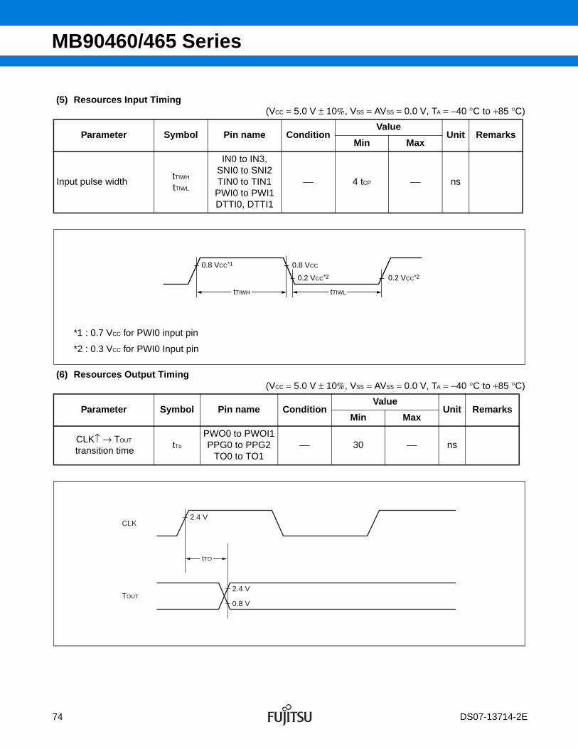
MB90460/465 Series
(5) Resources Input Timing (VCC = 5.0 V ± 10%, VSS = AVSS = 0.0 V, TA = −40 °C to +85 °C)
(6) Resources Output Timing (VCC = 5.0 V ± 10%, VSS = AVSS = 0.0 V, TA = −40 °C to +85 °C)
Parameter Symbol Pin name ConditionValue
Unit RemarksMin Max
Input pulse widthtTIWH
tTIWL
IN0 to IN3, SNI0 to SNI2TIN0 to TIN1PWI0 to PWI1DTTI0, DTTI1
⎯ 4 tCP ⎯ ns
Parameter Symbol Pin name ConditionValue
Unit RemarksMin Max
CLK↑ → TOUT
transition timetTo
PWO0 to PWOI1PPG0 to PPG2
TO0 to TO1⎯ 30 ⎯ ns
0.8 VCC*1 0.8 VCC
0.2 VCC*2 0.2 VCC*2
tTIWH tTIWL
*1 : 0.7 VCC for PWI0 input pin
*2 : 0.3 VCC for PWI0 Input pin
2.4 VCLK
TOUT0.8 V
2.4 V
tTO
74 DS07-13714-2E
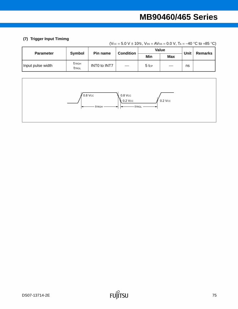
MB90460/465 Series
(7) Trigger Input Timimg (VCC = 5.0 V ± 10%, VSS = AVSS = 0.0 V, TA = −40 °C to +85 °C)
Parameter Symbol Pin name ConditionValue
Unit RemarksMin Max
Input pulse width tTRGH
tTRGLINT0 to INT7 ⎯ 5 tCP ⎯ ns
0.8 VCC 0.8 VCC
0.2 VCC 0.2 VCC
tTRGH tTRGL
DS07-13714-2E 75

MB90460/465 Series
5. A/D Converter Electrical Characteristics (3.0 V ≤ AVR − AVSS, VCC = AVCC = 5.0 V ± 10%, VSS = AVSS = 0.0 V, TA = −40 °C to +85 °C)
* : The current when the A/D converter is not operating or the CPU is in stop mode (for VCC = AVCC = AVR = 5.0 V)
Parameter Sym-bol
Pin name
ValueUnit Remarks
Min Typ Max
Resolution ⎯ ⎯ ⎯ 10 ⎯ bit
Total error⎯ ⎯ ⎯ ⎯ ±3.0 LSB
For MB90F462, MB90462, MB90F462A, MB90F463A, MB90467
⎯ ⎯ ⎯ ⎯ ±5.0 LSB For MB90V460
Non-linear error ⎯ ⎯ ⎯ ⎯ ±2.5 LSB
Differentiallinearityerror
⎯ ⎯ ⎯ ⎯ ±1.9 LSB
Zero transitionvoltage
VOTAN0 to
AN7
AVSS − 1.5 LSB
AVSS + 0.5 LSB
AVSS + 2.5 LSB
VFor MB90F462, MB90462, MB90F462A, MB90F463A, MB90467
AVSS − 3.5 LSB
AVSS + 0.5 LSB
AVSS + 4.5 LSB
V For MB90V460
Full-scale transitionvoltage
VFSTAN0 to
AN7
AVR − 3.5 LSB
AVR − 1.5 LSB
AVR + 0.5 LSB
VFor MB90F462, MB90462, MB90F462A, MB90F463A,MB90467
AVR − 6.5 LSB
AVR − 1.5 LSB
AVR + 1.5 LSB
V For MB90V460
Conversion time ⎯ ⎯ 6.125 ⎯ 1000 µs
Actual value is specified as a sum of values specified in ADCR0 : CT1, CT0 and ADCR0 : ST1, ST0. Be sure that the setting value is greater than the min value
Sampling period ⎯ ⎯ 2 ⎯ ⎯ µsActual value is specified in ADCR0 : ST1, ST0 bits. Be sure that the setting value is greater than the min value
Analog port inputcurrent
IAINAN0 to
AN7⎯ ⎯ 10 µA
Analog input voltage
VAINAN0 to
AN7AVSS ⎯ AVR V
Reference voltage ⎯ AVRAVSS +
2.7⎯ AVCC V
Power supply current
IAAVCC
⎯ 2.3 6 mAFor MB90F462, MB90F462A, MB90F463A, MB90462, MB90467
⎯ 2 5 mA For MB90V460
IAH* ⎯ ⎯ 5 µA *
Reference voltagesupply current
IRAVR
⎯ 140 260 µA For MB90F462, MB90462, MB90467
⎯ 600 900 µA For MB90F462A, MB90F463A
⎯ 0.9 1.3 mA For MB90V460
IRH* ⎯ ⎯ 5 µA *
Offset betweenchannels
⎯ AN0 to AN7
⎯ ⎯ 4 LSB
76 DS07-13714-2E

MB90460/465 Series
6. A/D Converter Glossary
(Continued)
Resolution : Analog changes that are identifiable with the A/D converterLinearity error : The deviation of the straight line connecting the zero transition point
(“00 0000 0000” ←→ “000000 0001”) with the full-scale transition point (“11 1111 1110” ←→ “11 1111 1111”) from actual conversion characteristics
Differential linearity error : The deviation of input voltage needed to change the output code by 1 LSB from the theoretical value
Total error : The total error is defined as a difference between the actual value and the theoretical value, which includes zero-transition error/full-scale transition error and linearity error.
3FF
3FE
3FD
004
003
002
001
AVss
Dig
ital o
utpu
t
AVRAnalog input
1.5 LSB
0.5 LSB
1 LSB × (N − 1) + 0.5 LSB
Actual conversionvalue
Actual conversionvalue
Theoreticalcharacteristics
VNT
(Measured value)
Total error
Total error for digital output N = VNT − 1 LSB × (N − 1) + 0.5 LSB
[LSB]1 LSB
1 LSB = (Theoretical value) AVR − AVSS
[V]1024
VOT (Theoretical value) = AVSS + 0.5 LSB [V]VFST (Theoretical value) = AVR − 1.5 LSB [V]VNT : Voltage at a transition of digital output from (N − 1) to N
DS07-13714-2E 77

MB90460/465 Series
(Continued)
3FF
3FE
3FD
004
003
002
001
AVss AVR AVss AVR
N + 1
N
N − 1
N − 2
VNT
V (N + 1) T
VOT (Measured value)
VFST
1 LSB × (N − 1) + VOT
Dig
ital o
utpu
t
Dig
ital o
utpu
t
Analog input Analog input
Actual conversionvalue
(Measuredvalue)
Actual conversionvalue
Theoreticalcharacteristics
(measured value)
Theoretical characteristics
Actual conversionvalue
(Measured value)
Actual conversionvalue
VNT
(Measured value)
Differential linearity errorLinearity error
Linearity error ofdigital output N
VNT − 1 LSB × (N − 1) + VOT =
1 LSB [LSB]
Differential linearity errorof digital output N
V (N + 1) T − VNT =
1 LSB −1 [LSB]
VFST − VOT =
1022 [V]1 LSB
VOT : Voltage at transition of digital output from “000H” to “001H”VFST : Voltage at transition of digital output from “3FEH” to “3FFH”
78 DS07-13714-2E
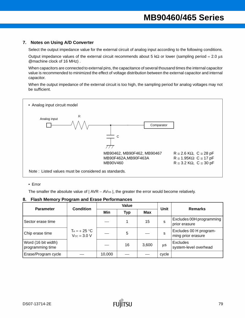
MB90460/465 Series
7. Notes on Using A/D Converter
Select the output impedance value for the external circuit of analog input according to the following conditions.
Output impedance values of the external circuit recommends about 5 kΩ or lower (sampling period = 2.0 µs@machine clock of 16 MHz) .
When capacitors are connected to external pins, the capacitance of several thousand times the internal capacitorvalue is recommended to minimized the effect of voltage distribution between the external capacitor and internalcapacitor.
When the output impedance of the external circuit is too high, the sampling period for analog voltages may notbe sufficient.
• Error
The smaller the absolute value of | AVR − AVSS |, the greater the error would become relatively.
8. Flash Memory Program and Erase Performances
Parameter ConditionValue
Unit RemarksMin Typ Max
Sector erase time
TA = + 25 °CVCC = 3.0 V
⎯ 1 15 sExcludes 00H programming prior erasure
Chip erase time ⎯ 5 ⎯ sExcludes 00 H program-ming prior erasure
Word (16 bit width) programming time
⎯ 16 3,600 µsExcludessystem-level overhead
Erase/Program cycle ⎯ 10,000 ⎯ ⎯ cycle
C
Comparator
Analog inputR
• Analog input circuit model
Note : Listed values must be considered as standards.
MB90462, MB90F462, MB90467MB90F462A,MB90F463A
R ≅ 2.6 KΩ, C ≅ 28 pFR ≅ 1.95KΩ C ≅ 17 pF
MB90V460 R ≅ 3.2 KΩ, C ≅ 30 pF
DS07-13714-2E 79

MB90460/465 Series
EXAMPLE CHARACTERISTICS• Power Suppy Current of MB90462, MB90467
40
35
30
25
20
15
10
5
02 3 4 5 6
ICC
H (
mA
)
FC = 16 [MHz]
FC = 12 [MHz]
FC = 10 [MHz]
FC = 8 [MHz]
FC = 4 [MHz]
FC = 2 [MHz]
VCC (V)
ICC
S (
mA
)2 3 4 5 6
FC = 4 [MHz]
FC = 12 [MHz]
FC = 16 [MHz]
FC = 10 [MHz]
FC = 8 [MHz]
FC = 2 [MHz]
20
18
16
14
12
10
8
6
4
2
0
VCC (V)
VC
C −
VO
H (
mV
)
IOH (mA)
1000
900
800
700
600
500
400
300
200
100
00 2 4 6 8 10 12− − − − − −
VO
L (V
)
IOL (mA)
1000
900
800
700
600
500
400
300
200
100
00 2 4 6 8 10 12
ICCH vs. VCC
TA = 25 °C, external clock inputICCS vs. VCC
TA = 25 °C, external clock input
VCC − VOH vs. IOH
TA = 25 °C, VCC = 4.5 VVOL vs. IOL
TA = 25 °C, VCC = 4.5 V
80 DS07-13714-2E
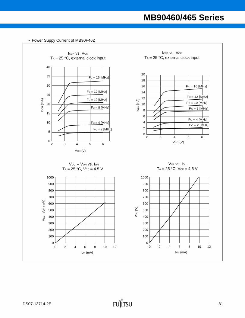
MB90460/465 Series
• Power Suppy Current of MB90F462
40
35
30
25
20
15
10
5
02 3 4 5 6
ICC
H (
mA
)
FC = 16 [MHz]
FC = 12 [MHz]
FC = 10 [MHz]
FC = 8 [MHz]
FC = 4 [MHz]
FC = 2 [MHz]
VCC (V)
ICC
S (m
A)
2 3 4 5 6
FC = 4 [MHz]
FC = 12 [MHz]
FC = 10 [MHz]
FC = 8 [MHz]
FC = 2 [MHz]
20
18
16
14
12
10
8
6
4
2
0
FC = 16 [MHz]
VCC (V)
VC
C -
VO
H (
mV
)
IOH (mA)
1000
900
800
700
600
500
400
300
200
100
00 2 4 6 8 10 12
VO
L (V
)
IOL (mA)
1000
900
800
700
600
500
400
300
200
100
00 2 4 6 8 10 12
ICCH vs. VCC
TA = 25 °C, external clock inputICCS vs. VCC
TA = 25 °C, external clock input
VCC − VOH vs. IOH
TA = 25 °C, VCC = 4.5 VVOL vs. IOL
TA = 25 °C, VCC = 4.5 V
DS07-13714-2E 81

MB90460/465 Series
• Power Suppy Current of MB90F462A/F463A
• Output Voltage of MB90F462A/F463A
0.0
5.0
10.0
15.0
20.0
25.0
30.0
35.0
40.0
1.0 2.0 3.0 4.0 5.0 6.0 7.0Vcc[V]
ICC [mA]Ta=25[ ]
FCH =16.0[MHz]
FCH =12.0[MHz]
FCH =10.0[MHz]
FCH =8.0[MHz]
FCH =4.0[MHz]
FCH =2.0[MHz]
0.0
2.0
4.0
6.0
8.0
10.0
12.0
14.0
16.0
18.0
20.0
1.0 2.0 3.0 4.0 5.0 6.0 7.0Vcc[V]
ICCS [mA]Ta=25[ ]
FCH =16.0[MHz]
FCH =12.0[MHz]
FCH =10.0[MHz]
FCH =8.0[MHz]
FCH =4.0[MHz]
FCH =2.0[MHz]
0.0
0.2
0.4
0.6
0.8
1.0
-10-8-6-4-20
VCC-VOH [V]Ta=25[ ]
IOH[mA]
Vcc=3.0[V]
Vcc=3.5[V]
Vcc=4.0[V]
Vcc=4.5[V]Vcc=5.0[V]Vcc=5.5[V]
Vcc=6.0[V]
0.0
0.2
0.4
0.6
0.8
0 2 4 6 8 10
VOL1 [V]Ta=25[ ]
IOL [mA]
cVcc=4.0[V]
Vcc=4.5[V]Vcc=5.0[V]Vcc=5.5[V]Vcc=6.0[V]
Vcc=3.0[V] Vcc=3.5[V]
0.00
0.05
0.10
0.15
0.20
0.25
0.30
0 2 4 6 8 10IOL [mA]
VOL2 [V]Ta=25[ ]
Vcc=3.0[V]
Vcc=3.5[V]
Vcc=4.5[V]Vcc=5.0[V]
Vcc=5.5[V]Vcc=6.0[V]
Vcc=4.0[V]
82 DS07-13714-2E

MB90460/465 Series
ORDERING INFORMATION
Part number Package Remarks
MB90F462PMCMB90F462APMCMB90F463APMCMB90462PMCMB90467PMC
64-pin Plastic LQFP (FPT-64P-M23)
MB90F462PFMB90F462APFMB90F463APFMB90462PFMB90467PF
64-pin Plastic QFP (FPT-64P-M06)
MB90F462P-SHMB90F462AP-SHMB90F463AP-SHMB90462P-SHMB90467P-SH
64-pin Plastic SH-DIP (DIP-64P-M01)
DS07-13714-2E 83

MB90460/465 Series
PACKAGE DIMENSIONS
Please confirm the latest Package dimension by following URL.http://edevice.fujitsu.com/package/en-search/
(Continued)
64-pin plastic QFP Lead pitch 1.00 mm
Package width ×package length
14 × 20 mm
Lead shape Gullwing
Sealing method Plastic mold
Mounting height 3.35 mm MAX
Code(Reference)
P-QFP64-14×20-1.00
64-pin plastic QFP(FPT-64P-M06)
(FPT-64P-M06)
C 2003-2008 FUJITSU MICROELECTRONICS LIMITED F64013S-c-5-6
0.20(.008) M
18.70±0.40(.736±.016)
14.00±0.20(.551±.008)
1.00(.039)
INDEX
0.10(.004)
1 19
20
3252
64
3351
20.00±0.20(.787±.008)
24.70±0.40(.972±.016)
0.42±0.08(.017±.003)
0.17±0.06(.007±.002)
0~8°
1.20±0.20(.047±.008)
3.00+0.35–0.20
(Mounting height).118
+.014–.008
0.25+0.15–0.20
.010+.006–.008
(Stand off)
Details of "A" part
"A"0.10(.004)
*
*
Dimensions in mm (inches).Note: The values in parentheses are reference values.
Note 1) * : These dimensions do not include resin protrusion.Note 2) Pins width and pins thickness include plating thickness.Note 3) Pins width do not include tie bar cutting remainder.
84 DS07-13714-2E
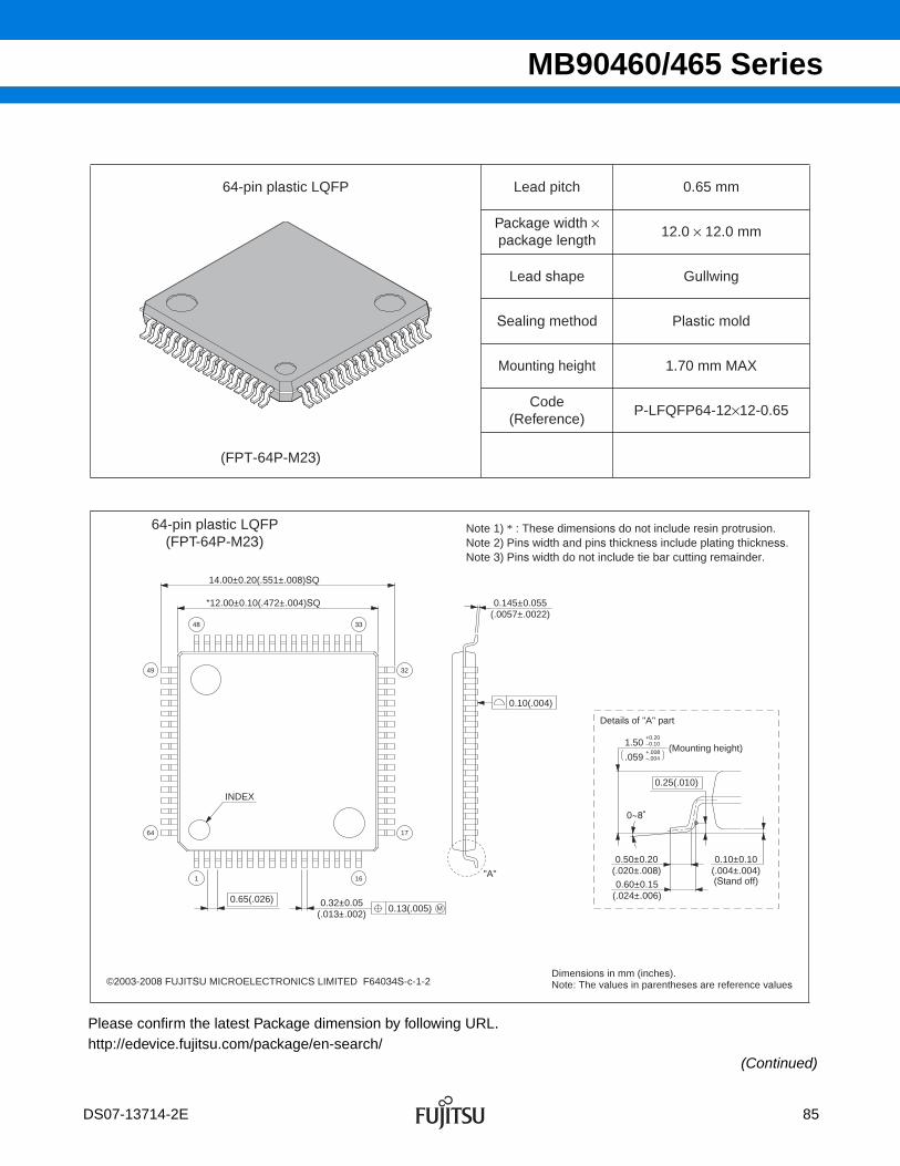
MB90460/465 Series
Please confirm the latest Package dimension by following URL.http://edevice.fujitsu.com/package/en-search/
(Continued)
64-pin plastic LQFP Lead pitch 0.65 mm
Package width ×package length
12.0 × 12.0 mm
Lead shape Gullwing
Sealing method Plastic mold
Mounting height 1.70 mm MAX
Code(Reference)
P-LFQFP64-12×12-0.65
64-pin plastic LQFP(FPT-64P-M23)
(FPT-64P-M23)
C 2003 FUJITSU LIMITED F64034S-c-1-1
0.65(.026)
0.10(.004)
1 16
17
3249
64
3348
*12.00±0.10(.472±.004)SQ
14.00±0.20(.551±.008)SQ
INDEX
0.32±0.05(.013±.002)
M0.13(.005)
0.145±0.055(.0057±.0022)
"A"
.059 –.004+.008
–0.10+0.20
1.50
0~8˚
0.25(.010)
(Mounting height)
0.50±0.20(.020±.008)0.60±0.15
(.024±.006)
0.10±0.10(.004±.004)
Details of "A" part
(Stand off)
Dimensions in mm (inches).Note: The values in parentheses are reference values©2003-2008 FUJITSU MICROELECTRONICS LIMITED F64034S-c-1-2
Note 1) * : These dimensions do not include resin protrusion.Note 2) Pins width and pins thickness include plating thickness.Note 3) Pins width do not include tie bar cutting remainder.
DS07-13714-2E 85

MB90460/465 Series
(Continued)
Please confirm the latest Package dimension by following URL.http://edevice.fujitsu.com/package/en-search/
64-pin plastic SH-DIP Lead pitch 1.778mm(70mil)
Package width ×package length
17 × 58 mm
Sealing method Plastic mold
Mounting height 5.65 mm MAX
64-pin plastic SH-DIP(DIP-64P-M01)
(DIP-64P-M01)
C 2001-2008 FUJITSU MICROELECTRONICS LIMITED D64001S-c-4-6
58.00+0.22–0.55
+.009–.0222.283
17.00±0.25(.669±.010)
3.30+0.20–0.30
.130 –.012+.008
+.028–.008.195
–0.20+0.70
4.95
+.016–.008.0543
–0.20+0.40
1.378 1.778(.0700) 0.47±0.10(.019±.004)
1.00+0.50–0
.039 –.0+.020
+.020–.007.028
–0.19+0.50
0.70
19.05(.750)(.011±.004)0.27±0.10
0~15
INDEX-2
INDEX-1
M0.25(.010)
Dimensions in mm (inches).Note: The values in parentheses are reference values.
Note: Pins width and pins thickness include plating thickness.
86 DS07-13714-2E

MB90460/465 Series
MAIN CHANGES IN THIS EDITION
The vertical lines marked in the left side of the page show the changes.
Page Section Change Results
⎯ ⎯ Changed the series name;MB90460 series→MB90460/465 series
⎯ ⎯ Added the part number;MB90F462A, MB90F463A
⎯ ⎯ Changed the package.(FPT-64P-M09 →FPT-64P-M23)
61, 62 PERIPHERAL RESOURCES16. 512/1024 Kbit Flash Memory
Added the 1024 Kbit flash memory.
74 ELECTRICAL CHARACTERISTICS4. AC Characteristics
Added the “(6) Resources Output Timing”
76 ELECTRICAL CHARACTERISTICS5. A/D Converter Electrical Characteristics
Changed the unit of “Zero transition voltage” and “Full-scale transition voltage”;mV → V
83
ORDERING INFORMATION Changed the part number; MB90462PFM →MB90462PMC MB90467PFM →MB90467PMC MB90F462PFM →MB90F462PMC
85 PACKAGE DIMENSIONS Changed the figure of package.
FPT-64P-M09 →FPT-64P-M23
DS07-13714-2E 87
MB90460/465 Series
FUJITSU MICROELECTRONICS LIMITED7-1, Nishishinjuku 2-chome, Shinjuku Dai-Ichi Seimei Bldg.,Shinjuku-ku, Tokyo 163-0722, JAPANTel: +81-3-5322-3347 Fax: +81-3-5322-3387http://jp.fujitsu.com/fml/en/
For further information please contact:
North and South AmericaFUJITSU MICROELECTRONICS AMERICA, INC.1250 E. Arques Avenue, M/S 333Sunnyvale, CA 94085-5401, U.S.A.Tel: +1-408-737-5600 Fax: +1-408-737-5999http://www.fma.fujitsu.com/
EuropeFUJITSU MICROELECTRONICS EUROPE GmbHPittlerstrasse 47, 63225 Langen, F. R. GERMANY Tel: +49-6103-690-0 Fax: +49-6103-690-122http://emea.fujitsu.com/microelectronics/
KoreaFUJITSU MICROELECTRONICS KOREA LTD.1002 Daechi-Dong, 206 KOSMO TOWER, Kangnam-Gu, Seoul 135-280, KOREATel: +82-2-3484-7100 Fax: +82-2-3484-7111http://www.fmk.fujitsu.com/
Asia PacificFUJITSU MICROELECTRONICS ASIA PTE LTD.151 Lorong Chuan, #05-08 New Tech Park,Singapore 556741, SINGAPORETel: +65-6281-0770 Fax: +65-6281-0220http://www.fujitsu.com/sg/services/micro/semiconductor/
FUJITSU MICROELECTRONICS SHANGHAI CO., LTD.No.222 Yan An Road(E), Rm.3102, Bund Center, Shanghai 200002, P. R. CHINATel: +86-21-6335-1560 Fax: +86-21-6335-1605http://cn.fujitsu.com/fmc/
FUJITSU MICROELECTRONICS PACIFIC ASIA LTD.11 Canton Road, 10/F., World Commerce Centre, Tsimshatsui, Kowloon, HONG KONGTel: +852-2377-0226 Fax: +852-2376-3269http://cn.fujitsu.com/fmc/tw
All Rights Reserved.
The contents of this document are subject to change without notice. Customers are advised to consult with sales representatives before ordering.The information, such as descriptions of function and application circuit examples, in this document are presented solely for the purposeof reference to show examples of operations and uses of FUJITSU MICROELECTRONICS device; FUJITSU MICROELECTRONICSdoes not warrant proper operation of the device with respect to use based on such information. When you develop equipment incorporat-ing the device based on such information, you must assume any responsibility arising out of such use of the information. FUJITSU MICROELECTRONICS assumes no liability for any damages whatsoever arising out of the use of the information.Any information in this document, including descriptions of function and schematic diagrams, shall not be construed as license of the useor exercise of any intellectual property right, such as patent right or copyright, or any other right of FUJITSU MICROELECTRONICSor any third party or does FUJITSU MICROELECTRONICS warrant non-infringement of any third-party's intellectual property right orother right by using such information. FUJITSU MICROELECTRONICS assumes no liability for any infringement of the intellectualproperty rights or other rights of third parties which would result from the use of information contained herein.The products described in this document are designed, developed and manufactured as contemplated for general use, including withoutlimitation, ordinary industrial use, general office use, personal use, and household use, but are not designed, developed and manufacturedas contemplated (1) for use accompanying fatal risks or dangers that, unless extremely high safety is secured, could have a serious effectto the public, and could lead directly to death, personal injury, severe physical damage or other loss (i.e., nuclear reaction control in nuclear facility, aircraft flight control, air traffic control, mass transport control, medical life support system, missile launch control inweapon system), or (2) for use requiring extremely high reliability (i.e., submersible repeater and artificial satellite).Please note that FUJITSU MICROELECTRONICS will not be liable against you and/or any third party for any claims or damages arisingin connection with above-mentioned uses of the products.Any semiconductor devices have an inherent chance of failure. You must protect against injury, damage or loss from such failures byincorporating safety design measures into your facility and equipment such as redundancy, fire protection, and prevention of over-currentlevels and other abnormal operating conditions.Exportation/release of any products described in this document may require necessary procedures in accordance with the regulations ofthe Foreign Exchange and Foreign Trade Control Law of Japan and/or US export control laws.The company names and brand names herein are the trademarks or registered trademarks of their respective owners.
Edited Business & Media Promotion Dept.