federal university of santa catarina - ufsc post-graduation in electrical engineering - ppgeel study...
TRANSCRIPT

Federal Federal UniversityUniversity of Santa of Santa Catarina - UFSCCatarina - UFSCPost-graduation in Electrical Engineering - PPGEELPost-graduation in Electrical Engineering - PPGEEL
Study and Design of a Voltage Line Conditioner Study and Design of a Voltage Line Conditioner with Serial Compensation and Fed by Load Sidewith Serial Compensation and Fed by Load Side
July, 2007
Master Thesis PresentationMaster Thesis Presentation::
Power Electronics Institute - INEPPower Electronics Institute - INEP
Eng. MSc Thiago Batista Soeiro
Presentation ContentsPresentation Contents
• • IntroductionIntroduction
• • Voltage Line Conditioner: Power StageVoltage Line Conditioner: Power Stage
• • Voltage Line Conditioner: Control StageVoltage Line Conditioner: Control Stage
• • Experimental ResultsExperimental Results
• • ConclusionsConclusions
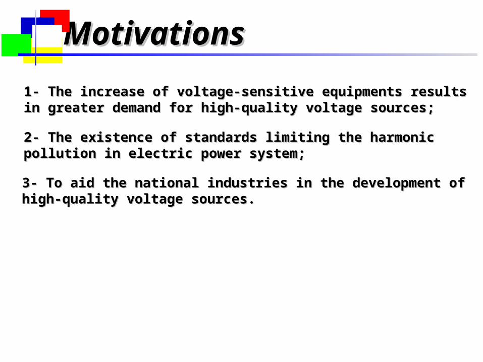
MotivationsMotivations
2- 2- The existence of standards limiting the harmonic pollution in The existence of standards limiting the harmonic pollution in electric power systemelectric power system;;
1- 1- The increase of voltage-sensitive equipments results in greater The increase of voltage-sensitive equipments results in greater demand for high-quality voltage sources;demand for high-quality voltage sources;
3- 3- To aid the national industries in the development of high-quality To aid the national industries in the development of high-quality voltage sources.voltage sources.

3- 3- To evaluate the performance of the topology proposed under To evaluate the performance of the topology proposed under unbalanced and distorted system voltagesunbalanced and distorted system voltages;;
Main ObjectivesMain Objectives
4- 4- To study and formulate control techniques to provide the To study and formulate control techniques to provide the conditioning of the load voltage conditioning of the load voltage
5- 5- To develop and test a voltage line conditioner prototype to To develop and test a voltage line conditioner prototype to validate the analysis.validate the analysis.
2- 2- To establish general voltage compensation methods to be applied To establish general voltage compensation methods to be applied in voltage line conditionersin voltage line conditioners;;
1- 1- To study concepts and topologies of voltage line conditionersTo study concepts and topologies of voltage line conditioners;;
1S
2S
3S
4S
5S
6S
7S
8S
oL
oC
a b
riv
dsv
Inverter
Rectifier
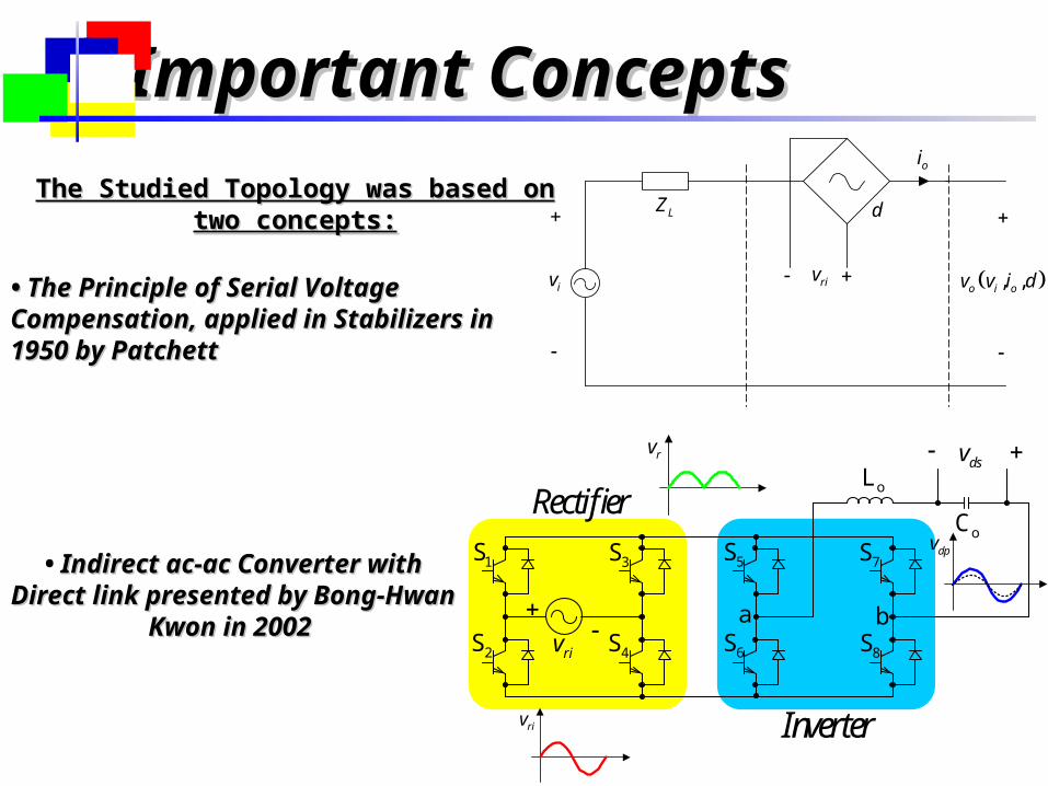
• • The The Principle of Serial Voltage Principle of Serial Voltage CompensationCompensation, applied in Stabilizers in , applied in Stabilizers in 1950 by Patchett 1950 by Patchett
The Studied Topology was based on two The Studied Topology was based on two concepts:concepts:
• Indirect ac-ac Converter with Indirect ac-ac Converter with Direct link presented by Bong-Direct link presented by Bong-
Hwan Kwon in 2002Hwan Kwon in 2002
riv
rv
dpv
Important ConceptsImportant Concepts
iv
oi
riv
, ,o i ov v i d
LZ d

The Voltage Line Conditioner Operation Principle:The Voltage Line Conditioner Operation Principle:
Important ConceptsImportant Concepts
i F Hv v v
o F Hi i i
riv
ov
iv dsv
ds dsF dsHv v v
ov
iv
SZ

Voltage Line Conditioner:Voltage Line Conditioner: Power StagePower Stage
+
-
1S
iv
2S
3S
4S6S
7S
8SoC
1T
a b
dsv
oL
S dsL L
5S
rv
Inverter Rectifier
Loiov
oi
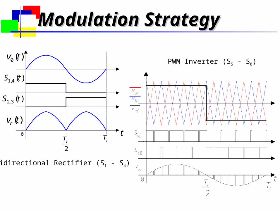
Modulation StrategyModulation Strategy
0
2rT rT
t
0( )v t
( )rv t
1,4 ( )S t
2,3 ( )S t
Bidirectional Rectifier (S1 - S4)
rT2rT
t0
abv
refv
Srrv
7,8S
5,6S
Srrv
PWM Inverter (S5 - S8)

Main WaveformsMain Waveforms
3 Level PWM Modulation
Rectifier
Inverter
iv
Adding voltage Subtracting voltage
0 2 0 2
1,4gv
2,3gv
rv
cv
abv
dsv
ov
iv
2sTd
2sT0
t t
ov
Rectifier input voltage Rectifier input voltage

Main Analytical ExpressionMain Analytical Expression
( )
Ng t
N d t
0 1
2Leqs eq
V d t d tI
N f L
2 1
16 4 1Leq o
CoS o S o Leq
I N d t I d t d tV
N f C f C I N d t N
Converter’s Static Gain
Voltage ripple
Transformation ratio
Current ripple
1N d t

Voltage Line Conditioner: Voltage Line Conditioner: Control StageControl Stage
T
a
6D
5D
b7D
8D 4D
3D
1D
D
0( )v t()iv t
1S 2S 3S 4S
_o refv5S 6S 7S 8S
SrrvSrrv
2
vC (s)
Sensorde
Tensão
Red
e de
Ene
rgia
SR SLdPL
Car
ga
Compensador de TensãoModulador
Modulador
5S
6S
7S
8S
1S
2S
3S
4S0C
Comando

Mathematical ModelMathematical Model
• • Small signals model:Small signals model: • G(s), Transfer Function of output voltage vs. duty cycle; • F(s), Transfer Function of output voltage vs. input voltage .
2
222 2
eq oo
Lo
eqeq o
L
s L N VV N D
Z N DvG s
s L Nds L C N N D
Z
2
22 2
o
eqieq o
L
N N DvF s
s L Nvs L C N N D
Z
0 iv s F s v s G s d s

Conditioner Analytical StudyConditioner Analytical Study
• • Load Influence over circuit’s dynamic responseLoad Influence over circuit’s dynamic response::

There are some strategies to damp the voltage oscillation or compensate the absence of load:
• • To damp voltage oscillation with virtual resistance control strategy;To damp voltage oscillation with virtual resistance control strategy;
• • To insert a control loop to compensate abrupt voltage drop;To insert a control loop to compensate abrupt voltage drop;
• To insert input filter topologiesTo insert input filter topologies;;
Conditioner Analytical StudyConditioner Analytical Study