downloads.semi.orgdownloads.semi.org/.../$file/5333.docx · web viewsemiconductor equipment and...
TRANSCRIPT
Background Statement for SEMI Draft Document 5333NEW STANDARD: TEST METHOD FOR IN-LINE MEASUREMENT OF WAVINESS OF PV SILICON WAFERS BY A LIGHT SECTIONING TECHNIQUE USING MULTIPLE LINE SEGMENTSNotice: This background statement is not part of the balloted item. It is provided solely to assist the recipient in reaching an informed decision based on the rationale of the activity that preceded the creation of this Document.
Notice: Recipients of this Document are invited to submit, with their comments, notification of any relevant patented technology or copyrighted items of which they are aware and to provide supporting documentation. In this context, “patented technology” is defined as technology for which a patent has issued or has been applied for. In the latter case, only publicly available information on the contents of the patent application is to be provided.
Today the dominant technology for slicing bricks to produce silicon wafers for photovoltaic solar cells is multiple wire sawing. With this technology it is possible to reliably produce wafers with thicknesses between 100 – 300 µm. Wire sawing is a mechanical process where steel wires with a diameter between 100 and 160 um are used to transport slurry into the cutting zone of the silicon brick or, in the case of diamond wire saws, cut the silicon directly using only a lubricant but not slurry. The slurry typically contains SiC particles, which remove the silicon material in an abrasive process. In case of a diamond wire small diamond pieces are attached to the steel wire. In both cases the abrasive process generates grooves and steps along the wire direction as well as waviness in the surface of the Si wafers. Saw marks and waviness negatively impact the quality of the wafers and subsequently the quality of the solar cell made from these wafers. Document 5333 focuses on the measurement of waviness and includes results of a Measurement System Analysis on a set of wafers.
Note: Measurement of saw marks is the topic of a related standard that was balloted successfully in June 2012.
The corresponding SNARF was approved by the PV Committee in its meeting in Dresden on October 11, 2011. The draft document was approved for yellow letter ballot in cycle 5 of 2012 by the PV Committee in its meeting in Munich on June 13, 2012, to be adjudicated in Dresden in October 2012.
Review and Adjudication InformationTask Force Review Committee Adjudication
Group: PV Silicon Materials TF Europe PV Materials CommitteeDate: Tuesday, October 9, 2012 Tuesday, October 9, 2012Time & Timezone: 10:00 to 12:00 CET 13:00 to 15:00 CETLocation: Messe Dresden Messe DresdenCity, State/Country: Dresden, Germany Dresden, GermanyLeader(s): Peter Wagner Peter Wagner
Hubert Aulich (PV Crystalox)Standards Staff: Yann Guillou
+33 4 3878 [email protected]
Yann Guillou+33 4 3878 [email protected]
This meeting’s details are subject to change, and additional review sessions may be scheduled if necessary. Contact the task force leaders or Standards staff for confirmation.
Check www.semi.org/standards under Calendar of Events for the latest update.

DRAFTDocument Number: 5333
Date: 5/6/23
SEMI Draft Document 5333NEW STANDARD: TEST METHOD FOR IN-LINE MEASUREMENT OF WAVINESS OF PV SILICON WAFERS BY A LIGHT SECTIONING TECHNIQUE USING MULTIPLE LINE SEGMENTS1 Purpose 1.1 Si wafers for PV applications cut from a Si ingot or Si brick by multiple wire sawing contain surface undulations/ripples characteristic for this cutting process, so called waviness.1.2 This waviness is a surface feature where the peaks and valleys of the waves are parallel to the wires of the saw and the direction of the wave is perpendicular to those wires.1.3 Waviness may significantly impact the quality of solar wafers.1.4 Waviness is frequently specified for Si wafers for solar cells as a maximum peak-to valley range.1.5 Therefore process and quality control during manufacturing of wafers requires continuous monitoring of saw marks and waviness with a method that provides reproducible values.
1.6 Process and quality control during manufacturing of wafers requires continuous monitoring of waviness with a non-contact method that supports high throughput.
2 Scope2.1 This test method determines the maximum peak-to-valley of waviness of multi or single crystal Si wafers that typically runs across the entire wafer surface and along the wire direction.2.2 This test method employs an in-line, non-contacting and non-destructive method for measuring the waviness of clean, dry as-cut silicon wafers supported by two belts that move the test specimen through the measurement equipment.2.3 This test method covers square and pseudo-square PV Si wafers, with a nominal edge length ≥ 125 mm and a nominal thickness ≥ 100 µm. It applies to both single-crystalline and multi-crystalline Si wafers.2.4 The test method is intended for in-line high throughput measurements. Therefore it is mandatory to operate the measurement system under statistical process control (SPC, e.g. ISO 11462) in order to obtain reliable, repeatable and reproducible measurement data.2.5 The test method is based on a light sectioning technique (see R1) where patterns of line segments or spots of light are projected onto a wafer surface and saw marks as well as the waviness peaks and valleys are oriented perpendicular to the direction of wafer transport.2.6 Other measurement techniques may also provide similar information about the waviness of a wafer as compared to this test method, but they are not the subject of this test method.
NOTICE: SEMI Standards and Safety Guidelines do not purport to address all safety issues associated with their use. It is the responsibility of the users of the Documents to establish appropriate safety and health practices, and determine the applicability of regulatory or other limitations prior to use.
3 Limitations3.1 Loading of wafers onto the measurement system must ensure that the waviness crests/valleys are transverse, not parallel, to the direction of travel through the measurement system. Measurements made on wafers loaded with waviness parallel to the direction of travel will not be suitable for characterizing the wafers’ surface topography.3.2 Wafer surface height vibration caused by transport during measurement may adversely impact measurements.3.3 The transverse locations where the measurements are taken on the wafer surface are critical. When comparing measurement results obtained by different equipment or by subsequent measurements on the same equipment it should be verified that the measurements are taken at the same transverse locations on the wafer surface.3.4 Measurement of waviness height variations depends on the physical setup of the measurement equipment, its opto-electronic noise level, and the calibration of measured signal to height.3.5 Variations of the projected light line image due to optical imperfections, including those of the wafer surface (such as grain boundaries or stains), may affect the measurement result.
This is a Draft Document of the SEMI International Standards program. No material on this page is to be construed as an official or adopted Standard or Safety Guideline. Permission is granted to reproduce and/or distribute this document, in whole or in part, only within the scope of SEMI International Standards committee (document development) activity. All other reproduction and/or distribution without the prior written consent of SEMI is prohibited.
Page 1 Doc. 5333 SEMI
Semiconductor Equipment and Materials International3081 Zanker RoadSan Jose, CA 95134-2127Phone: 408.943.6900, Fax: 408.943.7943
DRAFTDocument Number: 5333
Date: 5/6/23
3.6 Wafer saw marks may impact the waviness measurement results.
4 Referenced Standards and Document4.1 SEMI Standards and Safety Guidelines
SEMI E89 –– Guide for Measurement System Analysis (MSA)
SEMI M59 –– Terminology for Silicon Technology
SEMI MF1569 –– Guide for Generation of Consensus Reference Materials for Semiconductor Technology
4.2 ISO Standards1
ISO 11462-1 — Guidelines for implementation of statistical process control (SPC) – Part 1: Elements of SPC
ISO 11462-2 –– Guidelines for implementation of statistical process control (SPC) – Part 2: Catalogue of tools and techniques
NOTICE: Unless otherwise indicated, all documents cited shall be the latest published versions.
5 Terminology1: Refer to SEMI’s Compilation of Terms (COT) for a list of the most current terms and their definitions.
5.1 Terms and acronyms relating to silicon and other semiconductor technology are defined in SEMI M59.5.2 Other Abbreviations and Acronyms5.2.1 AOI –– angle of incidence5.2.2 COB –– center of brightness
5.3 Other Terms Used in this Standard
5.3.1 angle of incidence, of projected light line –– the angle between the line of sight of the projector and the surface normal (of the wafer).
5.3.2 center line, CL — an imaginary straight line bisecting a square or pseudo-square wafer surface. It is equidistant from opposing edges of the wafer surface.
5.3.3 center-of-brightness (COB) line –– a line fitted through a multiple pixel image representing the weighted average of the pixel values transverse to the projected line direction.5.3.4 pixel width and height, effective –– the distances on the wafer surface imaged by one picture element, or pixel, of the image sensor in perpendicular directions.5.3.5 saw mark –– a topographic step or groove along the sawing wire direction on the surface of a wafer, generated by the wire of the multiple wire saw.5.3.6 scan line –– an imaginary line parallel to a wafer edge and parallel to the wafer transport direction along which measurements are performed.5.3.7 waviness –– the more widely spaced component of surface texture (SEMI M59).
6 Summary of Test Method6.1 Four patterns of light line segments are projected on the wafer surface at an AOI as the wafer, resting on belts, is moved along in the x- direction, the direction of belt travel. These segments provide illumination for image acquisition along four scan lines.
6.1.1 The four scan lines are front-left (FL), back-left (BL), front-right (FR) and back-right (BR).
6.1.2 Each of these four projected light patterns are used identically to sample wafer topography at discrete transverse locations y, the direction perpendicular to the x-direction, ultimately producing N times four surface height variation profiles: H(x, yFL), H(x, yBL), H(x, yFR) and H(x, yBR), where N is the number of line segments in a pattern.
1 International Organization for Standardization, ISO Central Secretariat, 1 rue de Varembé, Case postale 56, CH-1211 Geneva 20, Switzerland; Telephone: 41.22.749.01.11, Fax: 41.22.733.34.30, http://www.iso.ch
This is a Draft Document of the SEMI International Standards program. No material on this page is to be construed as an official or adopted Standard or Safety Guideline. Permission is granted to reproduce and/or distribute this document, in whole or in part, only within the scope of SEMI International Standards committee (document development) activity. All other reproduction and/or distribution without the prior written consent of SEMI is prohibited.
Page 2 Doc. 5333 SEMI
Semiconductor Equipment and Materials International3081 Zanker RoadSan Jose, CA 95134-2127Phone: 408.943.6900, Fax: 408.943.7943
DRAFTDocument Number: 5333
Date: 5/6/23
6.2 When loaded onto the conveyor belt system the wafer is oriented such that:
6.2.1 The wafer’s waviness crests/valleys are perpendicular to the direction of belt travel.
6.2.2 Each projected light pattern illuminates the wafer surface at a distance from the nearest wafer edge.
6.3 Each projected pattern’s scattered light from the wafer surface is imaged by a camera system viewing the wafer surface at normal incidence. Alternatively the positions of projector and camera may be interchanged.6.4 Overlapping images of the projected light pattern scattered from the wafer surface are acquired during wafer transit.6.5 Height deviations from planar, along each scan line of the wafer surface, due to steps, grooves or waviness result in small transverse translations of the projected light pattern on the wafer surface that are recorded by the image of the projected light line segment (see R1).6.6 The images are processed and evaluated by an algorithm according to § 14 .
6.6.1 A calibration factor for each of the four projected light patterns image acquisition systems is determined using reference material with known step heights.
6.6.1.1 Small variations in the optical systems, such as the AOI of the projection and the actual viewing angle of the camera being slightly off-normal, make a purely geometrical calculation based on AOI less precise than is possible through calibration.
6.6.1.2 Calibration factors therefore are used to more precisely quantify surface height variation and reduce system-to-system measurement variation.
7 Interferences7.1 Vibrations of the test specimen relative to the probe-measuring axis may produce errors. Internal system monitoring may also be used to detect non-repetitive and repetitive system mechanical translations.7.2 Substantial variations in wafer surface properties may negatively impact the measurement result or possibly prevent measurement of some wafers.
7.2.1 Wafer surface roughness variation, along a scan line within a single wafer or between wafers, may impose signal to noise constraints on the optical system when imaging the light scatter from a nominally diffuse scattering surface.
7.3 Variation of pixel height and width within a camera system may not be corrected through the calibration.7.4 Mechanical variations in equipment adjustment may introduce errors.7.5 Temperature gradients across the measurement set-up may affect the measurement performance.7.6 Large surface defects, such as pits or chips, or contamination, such as slurry residue or particles, also may impact the measurement result.
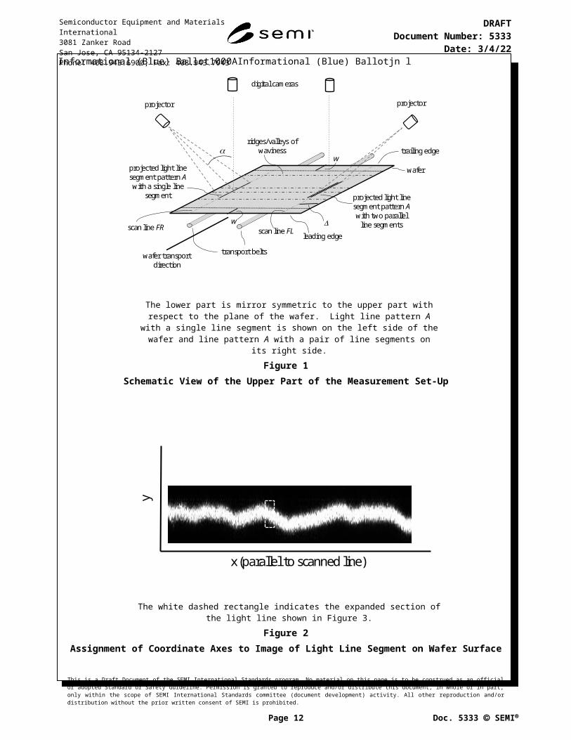
8 Apparatus (see Figure 1)8.1 Wafer transport device –– consisting of two belts, which transport the wafer continuously through the measurement apparatus without obstructing the projected light line or the line of sight of the cameras. The material of the belts shall not leave traces or residue on the wafer surface.8.2 Projector –– projecting one of the following patterns at an AOI onto the wafer surface at a distance from the wafer edge during transport.
8.2.1 Pattern A: N closely adjacent and equidistant parallel line segments that are oriented nominally parallel to the direction of belt travel. Typically N = 1 or N = 2, but more are possible. The distance between two adjacent line segments is denoted as .
8.2.2 Pattern B: N adjacent light spots (to be understood as limit of short line segments). Typically N = 1 or N = 2, but more are possible. The distance between two adjacent spots is denoted as .
8.2.3 The distance is measured from the wafer edges to the outmost part of the pattern.
8.3 In total four projectors are used, two above the wafer and two below the wafer.
This is a Draft Document of the SEMI International Standards program. No material on this page is to be construed as an official or adopted Standard or Safety Guideline. Permission is granted to reproduce and/or distribute this document, in whole or in part, only within the scope of SEMI International Standards committee (document development) activity. All other reproduction and/or distribution without the prior written consent of SEMI is prohibited.
Page 3 Doc. 5333 SEMI
Semiconductor Equipment and Materials International3081 Zanker RoadSan Jose, CA 95134-2127Phone: 408.943.6900, Fax: 408.943.7943
DRAFTDocument Number: 5333
Date: 5/6/23
8.4 Sensor –– an imaging digital camera system with an effective pixel width sw and an effective pixel height sh. It is set-up with its line of sight normal to the wafer surface, recording images of the projected light pattern on the wafer surface while in transit. In total four cameras are used, two above the wafer and two below the wafer.8.5 Computer –– for controlling the measurement system and equipped with software for synchronously acquiring and processing the camera images according to § 14.8.6 The positions of projectors and corresponding cameras may be interchanged, meaning that the projector AOI is normal and the camera views the wafer surface at an oblique angle.
9 Test Specimen9.1 Clean, dry Si wafers with an as-cut surface condition.
10 Safety Precautions10.1 The entire equipment has to be placed in a closed housing and has to be secured with a safety lock that stops the belts and safely switches the tool off when the housing is opened.10.2 If required by local, national or international safety requirements, eye protection goggles have to be used by operators and maintenance personnel.
11 Preparation of Apparatus11.1 The suitability of the equipment is determined by performing statistically based instrument repeatability and reproducibility study to ascertain whether the equipment is operating within the manufacture’s stated specification, e.g. according to SEMI E89.11.2 Align line pattern projectors and digital cameras with respect to the wafers to be measured according to the manual of the supplier of the equipment.11.3 Adjust the sensitivity of the camera and the light intensity of projected light pattern so that the intensity profile of the image of the light pattern in the camera extends over at least three digital intensity levels above the noise level of the camera while avoiding saturation and image bloom.11.4 Define the control limits for SPC for the measurement equipment with a set of selected wafers.
2: As this test method is intended for a high throughput, high volume measurement the equipment cannot be calibrated for measuring each individual wafer. Therefore careful SPC has to be performed.
12 Calibration and Standardization12.1 Each projection and camera imaging system is calibrated by using one or more reference wafers.12.2 The reference wafers shall contain topographic surface features with known step height.
12.2.1 Care has to be taken selecting a tool for establishing the surface feature heights or depths of the reference wafers. This tool has to be calibrated with traceable reference materials and be non-destructive, typically non-contact.
12.3 Measure the reference wafer(s) according to the procedure given in § 13, but omitting steps ¶¶ 14.4 and 14.5.12.4 Determine for each reference mark k the calibration factor fk by dividing the known step height/groove depth by the corresponding tk.12.5 Determine the mean calibration factor f for that imaging system for several surface features k from one or several wafers.
13 Procedure13.1 Adjust the equipment and calibrate it according to the instructions of the supplier.13.2 Determine the calibration factors f for each projection and camera imaging system.13.3 Verify the equipment is within SPC limits.13.4 Measure the wafer.13.4.1 Place a wafer horizontally on the transport belts.
This is a Draft Document of the SEMI International Standards program. No material on this page is to be construed as an official or adopted Standard or Safety Guideline. Permission is granted to reproduce and/or distribute this document, in whole or in part, only within the scope of SEMI International Standards committee (document development) activity. All other reproduction and/or distribution without the prior written consent of SEMI is prohibited.
Page 4 Doc. 5333 SEMI
Semiconductor Equipment and Materials International3081 Zanker RoadSan Jose, CA 95134-2127Phone: 408.943.6900, Fax: 408.943.7943
DRAFTDocument Number: 5333
Date: 5/6/23
13.4.1.1 Align the wafer so that two of its edges are parallel to, and the waviness crests/valleys are oriented perpendicular to, the direction of transport so that is within the range of 5 mm to 1/6 of wafer side length with a tolerance of ± 2 mm.
13.4.2 Move the wafer through the measurement set-up.13.4.3 Scan the entire length of the wafer.
13.4.4 For pattern A record successive, overlapping images Hj(x, yi,) of each projected pattern during the scan so that 100% wafer coverage across the four scan lines is ensured, where i denotes the scan line (FL, FR, BL and BR), j denotes the image recorded. The length of each Hj(x, yi) has to be much less than the length of the measured wafers.
13.4.5 For pattern B, combine successive images of the spot pattern so that images of line segments Hj(x, yi,) are obtained that cover 100 % of the wafer across the four scan lines.13.4.6 Process each Hj(x, yi) from all four projection and camera imaging systems according to § 14.13.4.7 Report the maximum peak-to-valley value of waviness of the wafer according to § 15.13.5 Repeat with the next wafer.
14 Calculations14.1 The following calculations are performed automatically within the instrument. An outline of the calculation structure is provided here to indicate the nature of the procedure. 14.2 The projected light pattern and its image recorded by the digital camera have a finite width extending over several pixels. Therefore the image of the light pattern consists of an array of pixels that has to be processed to generate a line representing the surface profile that can be evaluated with respect to saw marks.14.3 Define sampling points as follows for each line segment in Hj(x, yi) in order to calculate the waviness from the scanned measurement points.
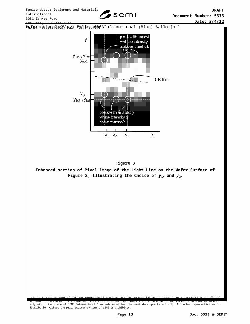
14.3.1 Assign a rectangular coordinate system to each Hj(x, yi) so that the x-axis is along the length of the line image(s) and the y-axis is perpendicular to the x-axis (Figure 2).
14.3.2 For each line image in a light pattern identify each pixel by a pair (x, yi) of integer index numbers, e.g. (215, 30), corresponding to the indices of the pixel in line 30 of column 215 of the pixel array.
14.3.3 Identify the gray-scale image brightness of the pixel at (x, yi) by In(x, yi) with n denoting the number of lines in the light pattern.
14.3.4 Image values typically range from 0 to 2M– 1, where M is the bit-depth of the image. Typical cameras use 8-bit images in unsigned integer format. In this case image brightness values span the range from 0 to 255 and use only 1 byte of data storage.
14.3.5 For each x-index value determine three yi-index values for each line image as follows:
14.3.5.1 Select a brightness threshold Ith that defines the signal level threshold clearly above noise level.
14.3.5.2 Determine ym,n(x) where In(x,yi) has its maximum.
14.3.5.3 Determine yl,n(x), the last y-index value where In(x ,yi) > Ith starting at ym,n(x) and going to increasing y-values.
14.3.5.4 Determine yu,n(x), the last y-index value where In(x, yi) > Ith starting at ym,n(x) and going to decreasing y-values.
14.3.6 Calculate the COB lines yCOB,n(x) for each line in the pattern by
yCOB , n( x )=∑ yl.n(x )
yu ,n (x )yi In ( x , yi )
∑ y l ,n( x)
yu ,n ( x)I n( x , y i)
(1)
This is a Draft Document of the SEMI International Standards program. No material on this page is to be construed as an official or adopted Standard or Safety Guideline. Permission is granted to reproduce and/or distribute this document, in whole or in part, only within the scope of SEMI International Standards committee (document development) activity. All other reproduction and/or distribution without the prior written consent of SEMI is prohibited.
Page 5 Doc. 5333 SEMI
Semiconductor Equipment and Materials International3081 Zanker RoadSan Jose, CA 95134-2127Phone: 408.943.6900, Fax: 408.943.7943
DRAFTDocument Number: 5333
Date: 5/6/23
with array indices x and yi, and the image brightness In(x, yi) at point (x, yi) of line n in the pattern with N lines in total.
14.4 Fit a straight line to each COB line (Figure 4).14.5 Subtract the fitted line from each COB line (Figure 4).14.6 Apply a moving-average filter of a fixed width of q sampling points to this line to smooth the resulting line2 (Figure 4).14.7 Calculate the peak-to-valley values ti,j,n(x) within a sliding window of a width of r sampling points for the smoothed line (Figure 4).NOTE 1: The following values for q and r have been found to provide stable and reproducible waviness results for wafers containing saw marks: q ≥ 1600 µm / sw, r ≥ 2 to 3·q, with sw in micrometers. For wafers without saw marks a smaller q may be sufficient.14.8 Calculate the height/depth hi,j,n(x) of the waviness by
(2)
14.9 Assign to hi,j(x) the maximum of all lines of a pattern by
(3)
14.10 Determine hmax as
(4)
and report it.
14.11 Optionally the waviness within a distance of w pixels from the leading and trailing edges, respectively, as well as the waviness between the boundaries of these regions of a wafer may be separately evaluated according to 14.3 to 14.10 (see Figure 1).
14.12 In this case, three values for the maximum waviness are reported: hmax,le, hmax,te and hmax,wi, with le, te and wi denoting leading edge, trailing edge and wafer interior, respectively.
15 Report15.1 The report shall contain the following elements.
15.1.1 Date and time of test.
15.1.2 Identification number of measurement equipment.
15.1.3 Software revision.
15.1.4 Calibration and SPC status of measurement equipment.
15.1.5 Ambient temperature.
15.1.6 Lot identification, including each wafer ID if available
15.1.7 Angle of incidence (AOI)
15.1.8 Line segment pattern used, A or B.
15.1.9 Number of lines segments or spots used.
2 See e.g. E.L. Church et al., Optical Engineering 24 (1985) 388 for theory of filtering.
This is a Draft Document of the SEMI International Standards program. No material on this page is to be construed as an official or adopted Standard or Safety Guideline. Permission is granted to reproduce and/or distribute this document, in whole or in part, only within the scope of SEMI International Standards committee (document development) activity. All other reproduction and/or distribution without the prior written consent of SEMI is prohibited.
Page 6 Doc. 5333 SEMI
Semiconductor Equipment and Materials International3081 Zanker RoadSan Jose, CA 95134-2127Phone: 408.943.6900, Fax: 408.943.7943
hi , j ,n( x )=t i , j , n( x ) f
hi , j( x )=max( hi , j , n( x ) )
hmax=max (h i , j )

DRAFTDocument Number: 5333
Date: 5/6/23
15.1.10 Distance , if multiple line segments of spots are used.
15.1.11 Effective pixel width sw and height sh.
15.1.12 Smoothing filter length q.
15.1.13 Evaluation window width r.
15.1.14 Distance w.
15.1.15 Maximum waviness hmax in micrometers, or hmax,le, hmax,te and hmax,wi in micrometers, if the option of ¶ 14.11 is used.
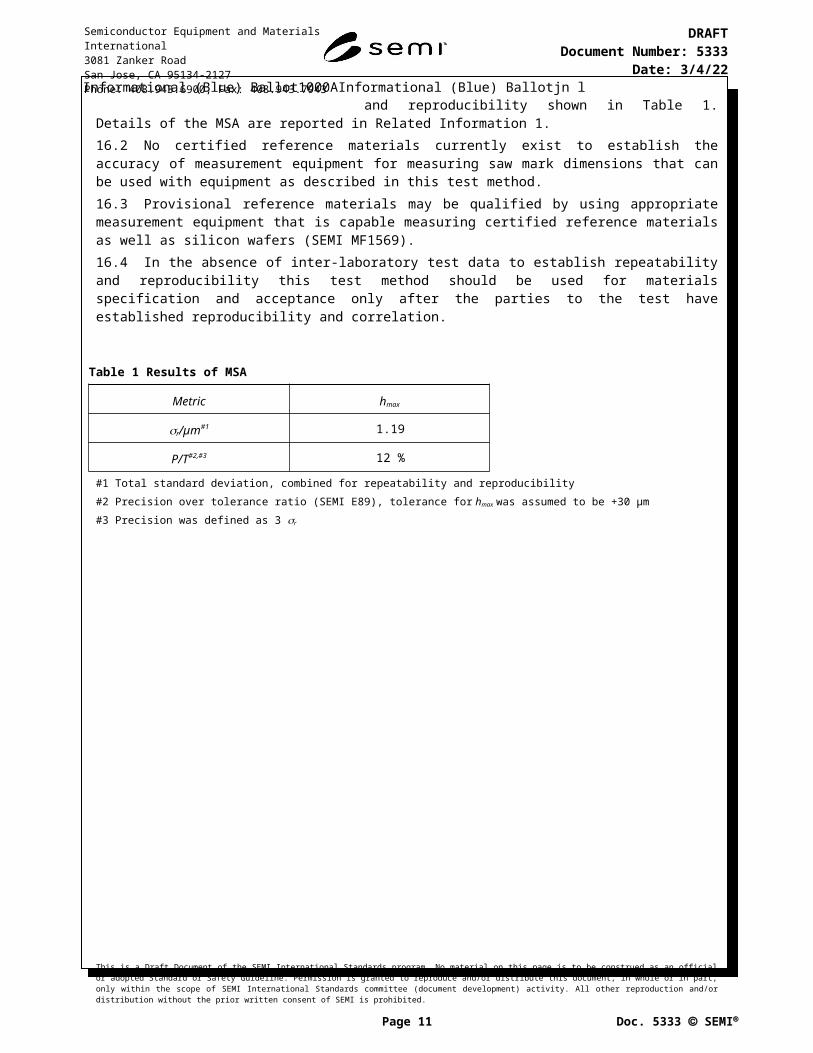
16 Precision and Accuracy16.1 The precision of the method has been determined experimentally by performing a MSA that provided the summarized results regarding repeatability and reproducibility shown in Table 1. Details of the MSA are reported in Related Information 1. 16.2 No certified reference materials currently exist to establish the accuracy of measurement equipment for measuring saw mark dimensions that can be used with equipment as described in this test method.16.3 Provisional reference materials may be qualified by using appropriate measurement equipment that is capable measuring certified reference materials as well as silicon wafers (SEMI MF1569).16.4 In the absence of inter-laboratory test data to establish repeatability and reproducibility this test method should be used for materials specification and acceptance only after the parties to the test have established reproducibility and correlation.
Table 1 Results of MSA
Metric hmax
r/µm#1 1.19
P/T#2,#3 12 %
#1 Total standard deviation, combined for repeatability and reproducibility#2 Precision over tolerance ratio (SEMI E89), tolerance for hmax was assumed to be +30 µm#3 Precision was defined as 3 r
This is a Draft Document of the SEMI International Standards program. No material on this page is to be construed as an official or adopted Standard or Safety Guideline. Permission is granted to reproduce and/or distribute this document, in whole or in part, only within the scope of SEMI International Standards committee (document development) activity. All other reproduction and/or distribution without the prior written consent of SEMI is prohibited.
Page 7 Doc. 5333 SEMI
Semiconductor Equipment and Materials International3081 Zanker RoadSan Jose, CA 95134-2127Phone: 408.943.6900, Fax: 408.943.7943

DRAFTDocument Number: 5333
Date: 5/6/23
NOTE: The lower part is mirror symmetric to the upper part with respect to the plane of the wafer. Light line pattern A with a single line segment is shown on the left side of
the wafer and line pattern A with a pair of line segments on its right side.Figure 1
Schematic View of the Upper Part of the Measurement Set-Up
NOTE: The white dashed rectangle indicates the expanded section of the light line shown in Figure 3.Figure 2
Assignment of Coordinate Axes to Image of Light Line Segment on Wafer Surface
This is a Draft Document of the SEMI International Standards program. No material on this page is to be construed as an official or adopted Standard or Safety Guideline. Permission is granted to reproduce and/or distribute this document, in whole or in part, only within the scope of SEMI International Standards committee (document development) activity. All other reproduction and/or distribution without the prior written consent of SEMI is prohibited.
Page 8 Doc. 5333 SEMI
x (parallel to scanned line)
y
digital cameras
wafer transport direction
projector
wafer
projector
projected light line segment pattern A with two parallel
line segments
projected light line segment pattern A with a single line
segment
ridges/valleys of waviness
scan line FLscan line FR
transport belts
w
w
leading edge
trailing edge
Semiconductor Equipment and Materials International3081 Zanker RoadSan Jose, CA 95134-2127Phone: 408.943.6900, Fax: 408.943.7943
DRAFTDocument Number: 5333
Date: 5/6/23
Figure 3Enhanced section of Pixel Image of the Light Line on the Wafer Surface of Figure 2, Illustrating the Choice of
yu,x and yl,x.
This is a Draft Document of the SEMI International Standards program. No material on this page is to be construed as an official or adopted Standard or Safety Guideline. Permission is granted to reproduce and/or distribute this document, in whole or in part, only within the scope of SEMI International Standards committee (document development) activity. All other reproduction and/or distribution without the prior written consent of SEMI is prohibited.
Page 9 Doc. 5333 SEMI
yu,x1
yu,x2 , yu,x3
yl,x1yl,x2 , yl,x3
x1 x2 x3 x
y pixels with largest y where intensity is above threshold
pixels with smallest y where intensity is above threshold
COB line
Semiconductor Equipment and Materials International3081 Zanker RoadSan Jose, CA 95134-2127Phone: 408.943.6900, Fax: 408.943.7943
DRAFTDocument Number: 5333
Date: 5/6/23
Figure 4Illustration of the Processing Steps for Evaluating the Peak-to-valley Value from the Digital Image of the
Light Line Trace
This is a Draft Document of the SEMI International Standards program. No material on this page is to be construed as an official or adopted Standard or Safety Guideline. Permission is granted to reproduce and/or distribute this document, in whole or in part, only within the scope of SEMI International Standards committee (document development) activity. All other reproduction and/or distribution without the prior written consent of SEMI is prohibited.
Page 10 Doc. 5333 SEMI
y/a.
u.Image of light line trace
COB line and line fit (dashed)
subtraction of fit from COB line
moving average filter
peak-to-valley evaluation
maximum peak-to-valley
x/a.u.
Semiconductor Equipment and Materials International3081 Zanker RoadSan Jose, CA 95134-2127Phone: 408.943.6900, Fax: 408.943.7943
DRAFTDocument Number: 5333
Date: 5/6/23
RELATED INFORMATION 1 RECOMMENDED PARAMETER SETTINGS AND MSANOTICE: This Related Information is not an official part of SEMI doc. 5333 and was derived from the work of the global PV Materials Technical Committee. This Related Information was approved for publication by full letter ballot procedures on [A&R approval date].
R1-1 PurposeR1-1.1 The settings of parameters , q, r, s, w significantly impact the outcome of a waviness measurement. Therefore a set of parameters is provided that enables reproducible measurements and that is widely used.
R1-2 Parameter SettingsR1-2.1 The following settings for the parameters are recommended:
= 76° q = 40 r = 230 sh = 20 µm w = 200
R1-3 Geometrical ResolutionR1-3.1 The fundamental relation between the waviness height/depth (h), the AOI (with respect to surface normal) and the measured offset a of the light trace due to the higher/lower surface of the waviness as compared to the adjacent surface is as follows (see Figure R1-1):
a=h tan α . (R1-1)
R1-3.2 A change in height/depth (h) results then in a change a based on equation R1-1 and assuming a constant angle :
Δa=Δh tan α . (R1-2)
R1-3.3 Assuming that the minimum a that can be detected by the system equals the effective pixel height sh one obtains with the parameters settings of R1-2.1 a height/depth resolution of the measurement set-up of
Δh=sh
tan α=20 µm
tan76 °=5.0 µm
. (R1-3)
This is a Draft Document of the SEMI International Standards program. No material on this page is to be construed as an official or adopted Standard or Safety Guideline. Permission is granted to reproduce and/or distribute this document, in whole or in part, only within the scope of SEMI International Standards committee (document development) activity. All other reproduction and/or distribution without the prior written consent of SEMI is prohibited.
Page 11 Doc. 5333 SEMI
Semiconductor Equipment and Materials International3081 Zanker RoadSan Jose, CA 95134-2127Phone: 408.943.6900, Fax: 408.943.7943
DRAFTDocument Number: 5333
Date: 5/6/23
h
a
projector
camera
projected line
projected line
wafer surface
Figure R1-1 Schematic Drawing of Basics of Light Sectioning Technique
R1-3.4 Therefore the minimum surface height variation that can be detected based on geometrical considerations is 5.0 µm.R1-3.5 However, the light trace on the wafer surface is a line the image of which is several pixels wide in the y-direction (see Figures 3 and 4) displaying an intensity profile. Therefore smaller height changes may be detected with the techniques as described in §14 by evaluating the intensity profile of the line image.
R1-4 Results of MSAR1-4.1 Test specimen –– 3 wafers 156 × 156 mm2.R1-4.2 Test conditions –– 30 repeats twice per day on 4 days, performed with the settings as described in R1-2.1.R1-4.3 Light pattern used –– Pattern A with a single line segment.R1-4.4 Results –– in Table R1-1 the mean values and standard deviations per day and per wafer are reported for hmax. The mean and the standard deviation per wafer (over 4 days) are reported in Table R1-2. The results of the individual measurements per day and per repeat are displayed in Figure R1-2.
Table R1-1 Results of MSA, mean and standard deviation per wafer and per day
Wafer Day hmax mean/µm hmax std.dev./µm
1 1 11.5 0.771 2 11.1 0.951 3 10.0 0.601 4 10.8 0.562 1 31.7 1.062 2 32.3 0.762 3 32.0 1.252 4 30.9 0.863 1 67.1 1.323 2 68.3 1.003 3 68.9 1.173 4 68.3 1.10
This is a Draft Document of the SEMI International Standards program. No material on this page is to be construed as an official or adopted Standard or Safety Guideline. Permission is granted to reproduce and/or distribute this document, in whole or in part, only within the scope of SEMI International Standards committee (document development) activity. All other reproduction and/or distribution without the prior written consent of SEMI is prohibited.
Page 12 Doc. 5333 SEMI
Semiconductor Equipment and Materials International3081 Zanker RoadSan Jose, CA 95134-2127Phone: 408.943.6900, Fax: 408.943.7943
DRAFTDocument Number: 5333
Date: 5/6/23
Table R1-2 Results of MSA, mean and standard deviation per wafer
Wafer hmax mean/µm hmax std.dev./µm
1 11.1 0.782 31.0 1.263 68.1 1.32
Figure R1-2 Results of Daily Measurements of Waviness
NOTICE: Semiconductor Equipment and Materials International (SEMI) makes no warranties or representations as to the suitability of the Standards and Safety Guidelines set forth herein for any particular application. The determination of the suitability of the Standard or Safety Guideline is solely the responsibility of the user. Users are cautioned to refer to manufacturer’s instructions, product labels, product data sheets, and other relevant literature, respecting any materials or equipment mentioned herein. Standards and Safety Guidelines are subject to change without notice.
By publication of this Standard or Safety Guideline, SEMI takes no position respecting the validity of any patent rights or copyrights asserted in connection with any items mentioned in this Standard or Safety Guideline. Users of this Standard or Safety Guideline are expressly advised that determination of any such patent rights or copyrights, and the risk of infringement of such rights are entirely their own responsibility.
This is a Draft Document of the SEMI International Standards program. No material on this page is to be construed as an official or adopted Standard or Safety Guideline. Permission is granted to reproduce and/or distribute this document, in whole or in part, only within the scope of SEMI International Standards committee (document development) activity. All other reproduction and/or distribution without the prior written consent of SEMI is prohibited.
Page 13 Doc. 5333 SEMI
5
10
15
20
25
30
35
40
45
50
55
60
65
70
75
1 11 21 1 11 21 1 11 21 1 11 21 1 11 21 1 11 21 1 11 21 1 11 21
h max
/μm
Day and RepeatsWafer_1 Wafer_2 Wafer_3
Day 1Meas. 1
Day 1Meas. 2
Day 2Meas. 1
Day 2Meas. 2
Day 3Meas. 1
Day 3Meas. 2
Day 4Meas. 1
Day 4Meas. 2
Semiconductor Equipment and Materials International3081 Zanker RoadSan Jose, CA 95134-2127Phone: 408.943.6900, Fax: 408.943.7943