final technical progress report/67531/metadc878844/m2/1/high_res... · polymer oled white light...
TRANSCRIPT

Polymer OLED White Light Development Program – (#DE-FC26-04NT41947) | Final Report page 1 of 111
Final Technical Progress Report Polymer OLED White Light Development Program – (#DE-FC26-04NT41947)
Submitted to: US Department of Energy (DOE) National Energy Technology Laboratory (NETL) Submitted by: OSRAM Opto-Semiconductors, Inc.
Program Director: Dr. Homer Antoniadis
Project/Task Managers and Key Contributors: Dr. Vi-En Choong (Task 1 Manager) Dr. Stelios Choulis (Task 1) Dr. Brian Cumpston (Task 2 Manager and Head of Process Development Group) Dr. Rahul Gupta (Task 3 Manager) Dr. Mathew Mathai (Task 1) Mr. Michael Moyer (Task 4 Manager) Dr. Franky So (Head of Materials and Device Group)
Submission date: 19 December 2005

Polymer OLED White Light Development Program – (#DE-FC26-04NT41947) | Final Report page 2 of 111
Table of Contents
1. EXECUTIVE SUMMARY ............................................................................................................. 5
2. EXPERIMENTAL........................................................................................................................ 9 2.1. Materials and Devices........................................................................................................9 2.2. White Tile Fabrication........................................................................................................9 2.3. RGB Tile Fabrication........................................................................................................11 2.4. Tile Testing .......................................................................................................................11 2.5. Reliability Testing ............................................................................................................12 3. TASK 1: WHITE EMITTING DEVICE DEVELOPMENT............................................................... 13 3.1. Introduction ........................................................................................................................13 3.2. Findings ..............................................................................................................................13 3.3. Year 1 Summary.................................................................................................................14 3.4. Year 2 Summary.................................................................................................................17 3.5. Year 2 Report Outline ........................................................................................................18 3.6. Experimental ......................................................................................................................19 3.7. Green PHOLEDs.................................................................................................................19
3.7.1. Improving Hole Injection Properties: .........................................................................................................20 3.7.2. Improving Electron Injection......................................................................................................................22
3.8. Yellow PHOLED..................................................................................................................24 3.9. Red PHOLEDs ....................................................................................................................24 3.10. Blue PHOLEDs .................................................................................................................25 3.11. Single layer White PHOLEDs ..........................................................................................27
3.11.1. Single layer RGB White PHOLEDs.........................................................................................................27 3.11.2. Single Layer RYB White PHOLEDs .......................................................................................................28
3.12. Generation of White Light by the Means of Down-conversion....................................30 3.12.1. Cool white light emitting device based on blue PHOLED .......................................................................31 3.12.2. Novel Approach to Generate Illumination Quality Light Based on Bluish-Green Emitting OLEDs .......34
3.12.2.1. Example: White Light Emitting Device Based on a Bluish-Green Emitting PHOLED ...................34 3.13. Light Extraction................................................................................................................35
3.13.1. Effect of Charge Balance and Micro-cavity Effects in Resultant Efficiency of OLEDs ..........................36 3.13.2. Brightness Enhancement Film..................................................................................................................37
3.14. Improving Emission Rate................................................................................................38 3.15. Future Work: Strategy for 40 lm/W White Source.........................................................39 3.16. Conclusions .....................................................................................................................39 4. TASK 2: WHITE TILE DESIGN, FABRICATION, AND TEST ....................................................... 40 4.1. Summary Description........................................................................................................40 4.2. Detailed Description ..........................................................................................................40

Polymer OLED White Light Development Program – (#DE-FC26-04NT41947) | Final Report page 3 of 111
4.2.1. Tile Fabrication ..........................................................................................................................................40 4.2.2. Designs .......................................................................................................................................................41 4.2.3. White Emitter Process Development..........................................................................................................43 4.2.4. Efficiency ...................................................................................................................................................45 4.2.5. Demonstration Panels .................................................................................................................................46
4.3. Characterization of Electrically Leaky Lighting Devices ...............................................47 4.3.1. The Origin of Leaky Paths..........................................................................................................................47 4.3.2. Correlation between IR Signature and I-V Characteristics.........................................................................47 4.3.3. Luminance Lifetime Behavior on OLED Lighting Devices with Electrically Leaky Paths .......................48 4.3.4. Methods to Avoid Leaky Paths During Manufacturing..............................................................................49 4.3.5. Burn-in Methods to Suppress Electrically Leaky Paths .............................................................................50
5. TASK 3: COLOR TUNABLE TILE DESIGN, FABRICATION, AND TEST....................................... 51 5.1. Introduction and Summary of Results ...........................................................................51 5.2. Experimental Results and Discussions .........................................................................52
5.2.1. Substrate Design ........................................................................................................................................52 5.2.2. Equipment Requirements to Achieve the Goals ........................................................................................53 5.2.3. Test set and Driver Design and Development ...........................................................................................54 5.2.4. Ink Development .......................................................................................................................................54
4.3.5.1. LEP Inks .............................................................................................................................................55 4.3.5.1. Jetting Stability of Inks .......................................................................................................................57 4.3.5.1. Shelf Life of Inks ................................................................................................................................57
5.2.5. Inkjet Process Development ......................................................................................................................58 4.3.5.1. Plasma Process....................................................................................................................................58 4.3.5.1. PEDOT Printing: ................................................................................................................................58 4.3.5.1. LEP Printing .......................................................................................................................................59
5.2.6. Year 1 Deliverable: Green Monochrome Tile ...........................................................................................60 5.2.7. End of Year 1 status and Goals for Year 2 ................................................................................................61 5.2.8. Scaling Up to 200 mm Plates.....................................................................................................................61
4.3.5.1. Plasma Process....................................................................................................................................61 4.3.5.1. PEDOT Printing..................................................................................................................................63
5.2.9. Optimization of RGB Printing...................................................................................................................63 4.3.5.1. Drying Stains ......................................................................................................................................63 4.3.5.1. Pixel Filling ........................................................................................................................................64 4.3.5.1. Baking of LEP ....................................................................................................................................65 4.3.5.1. Improving Fill Factor..........................................................................................................................66
5.2.10. Choosing the Best Ink ..........................................................................................................................66 5.2.11. RGB Demonstrators .............................................................................................................................67
4.3.5.1. Horizontal Intensity Drop: Resistive Drop in the Anode....................................................................68 4.3.5.1. Vertical Intensity Drop: Leakage Currents .........................................................................................70 4.3.5.1. Bright Lines ........................................................................................................................................70 4.3.5.1. Color Gamut of RGB Tiles and Efficiency of White..........................................................................71
5.2.12. Leakage Currents..................................................................................................................................72 4.3.5.1. Source of Leakage: Bulk Leakage vs. Point Defects ..........................................................................73 4.3.5.1. Identifying the Source of Bulk Leakage .............................................................................................74 4.3.5.1. Reduction of Point Defects .................................................................................................................75
5.2.13. Improving the Fill Factor .....................................................................................................................75 5.3. Conclusions......................................................................................................................77 6. Task 4: LIGHT MODULE AND DRIVER DESIGN DEVELOPMENT............................................. 78 6.1. Year 1 Lighting Module Driver Designs ...........................................................................78
6.1.1. AC Driver Scheme Investigation................................................................................................................78 6.1.2. Driver Design for Single Pixel Tile Light Source ......................................................................................79 6.1.3. Driver Design of Stripped Light Source .....................................................................................................80

Polymer OLED White Light Development Program – (#DE-FC26-04NT41947) | Final Report page 4 of 111
6.2. Year 2 Lighting Module Driver Designs ...........................................................................80 6.2.1. AC Drive Scheme Investigation .................................................................................................................80 6.2.2. Design of the Color Tunable Light Source.................................................................................................82
7. CONCLUSIONS ........................................................................................................................ 84
8. References............................................................................................................................. 85
9. LIST OF PUBLICATIONS.......................................................................................................... 86 9.1. Patents Filed.......................................................................................................................86 9.2. Refereed Journal Publications .........................................................................................87 9.3. Refereed Conference Proceedings papers .....................................................................87 9.4. Conference Presentations ................................................................................................88 Appendix A: Optical Effects and Location of Excitons in Blue devices..............................89 Appendix B: Effect of Charge Balance and Micro-cavity......................................................90
Appendix B.2 Micro-cavity Theory and Optical Modeling..................................................................................90 Appendix B.3 Results and Discussion..................................................................................................................92
Appendix C: General Method to Evaluate Substrate Surface Modification Techniques for Light Extraction Enhancement of OLEDs...............................................................................97
Appendix C.2 Fabrication of OLEDs ...................................................................................................................97 Appendix C.3 Brightness Enhancement Film ......................................................................................................98 Appendix C.4 Measurement of Substrate Mode and External Mode Intensity ....................................................98 Appendix C.5 Results and Discussion..................................................................................................................98
Appendix D: Improving Emission Rate.................................................................................101 List of Figures .........................................................................................................................105 List of Tables...........................................................................................................................111

Polymer OLED White Light Development Program – (#DE-FC26-04NT41947) | Final Report page 5 of 111
1. EXECUTIVE SUMMARY OSRAM Opto Semiconductors (OSRAM) successfully completed development, fabrication and characterization of the large area, polymer based white light OLED prototype at their OLED Research and Development (R&D) facility in San Jose, CA. The program, funded by the Department of Energy (DOE), consisted of three key objectives:
Develop new polymer materials and device architectures – in order to improve the performance of organic light emitters.
Develop processing techniques – in order to demonstrate and enable the manufacturing of large area, white light and color tunable, solid state light sources.
Develop new electronics and driving schemes for organic light sources, including color-tunable light sources.
The key performance goals are listed in Table 1.1 below.
Year 1 Year 2
Luminous Efficacy (lm/W) 7 20
Luminance Level (nits) 250 400
Operating Life (hrs @ 25 C) 2,000 3,000
Shelf Life at ambient (years) 5 5
CRI >80 >85
Major milestones (light module) 3”x5” - 2 tiles 6”x10”- 8 tiles
Table 1.1: Summary of milestones and deliverables.
A world record efficiency of 25 lm/W was established for the solution processed white organic device from the significant improvements made during the project. However, the challenges to transfer this technology from an R&D level to a large tile format such as, the robustness of the device and the coating uniformity of large area panels, remain. In this regard, the purity and the blend nature of the materials are two factors that need to be addressed in future work.
During the first year, OSRAM’s Materials and Device group (M&D) worked closely with the major polymer material suppliers to develop the polymer emissive technology. M&D was successful in demonstrating a 7-8 lm/W white light source which was based on fluorescent materials. However, it became apparent that the major gains in efficiency could only be made if phosphorescent materials were utilized. Thus, in order to improve the performance of the resulting devices, the focus of the project shifted towards development of solution-processable phosphorescent light emitting diodes (PHOLEDs) and device architectures. The result is a higher efficiency than the outlined project milestone. (See Table 1.2)

Polymer OLED White Light Development Program – (#DE-FC26-04NT41947) | Final Report page 6 of 111
G reen (hybrid) 50 55 0.33 0.60
Red 7 7 0.66 0.33
B lue 14 25 0.17 0.37
W hite s ingle layer 16 (20 w ith ligh t extraction) 27 0.29 0.43
W hite by down convers ion 25 39 0.26 0.40
Effic iency Lm /W Cd/A
CIE Coord inates x y
Table 1.2: Summary of the device performance achieved using PHOLEDs.
The progress in material performance can only be achieved by developing a deep understanding of charge transport, injection, trapping, energy-transfer and quenching mechanisms in PHOLEDs. Furthermore, techniques were developed to improve light extraction and enhance the external quantum efficiency. This included using other well known methods of the field, such as nano-particles at the interfaces of organic layers and brightness enhancing films. (See Section 3)
While the M&D group was improving the basic device performance of materials, the Process Development group was scaling up the fabrication processes to make large area light sources. Some of their objectives were to explore different design possibilities of a large-area OLED lighting tile, as well as, optimize the uniformity, efficiency, and reliability. Additionally, they were to optimize the processing conditions for working with the materials identified by the M&D group. Process Development was also tasked with making the demonstrators for the DOE.
During the first year, two designs were evaluated for use in lighting applications, and were used to scale up the processes identified in Task 1 to our 8" pilot line. These designs were both 2"x3" size; one using a striped pattern and one using a single, unpatterned emissive area. Each 8” plate comprised of six 2”x3” lighting tiles; processing conditions were optimized to achieve maximum efficiency, CRI, and uniformity. Tiles with uniform illumination single “pixel” designs were used in the demonstrators DOE received at the end of the first year. However, during that time, the non-uniformities in the lighting tile emission still existed and could not be completely eliminated.
The second year, the strategy to develop large panels was refined. The decision was made to use arrays of smaller, square, tiles to improve uniformity and yields. The small tiles were then used to make a 6”x10” demonstrator (Figure 1.1), which the DOE will receive with this report. These demonstrators are proof of the OLED manufacturing process scalability and the technological ability to deliver a variety of lighting panel sizes. Although most of the work was focused on fluorescent polymers, resulting in a luminous efficacy of 7-8 lm/W, a process was developed to create devices using the phosphorescent materials made by the M&D group. The challenge will be to transfer the research performance of a single layer white PHOLED achieved to a larger tile format in the Process Development Line.

Polymer OLED White Light Development Program – (#DE-FC26-04NT41947) | Final Report page 7 of 111
Figure 1.1: Image of a 6”x10” demonstrator, along with a 3”x5” demonstrator from first year.
In addition to making white emitting tiles, the Process Development group explored an approach to make color tunable light sources utilizing sub-millimeter striping and ink-jet printing technology. Inkjet printing was used to pattern the red, green and blue polymers at a sub-millimeter scale. Major efforts were focused to develop the tools for plasma processing and ink-jet printing necessary to create a process on 8” plates. Several new inks were developed to achieve the required film uniformity and process reliability on 8” plates. To improve the device performance they faced the challenge of reducing the print defects. The ink and process development was necessary to move inkjet printing from the realm of pictures and documents to the realm of thin film based optoelectronic devices. A color tunable demonstrator was made using fluorescent RGB polymers, as shown in Figure 1.2.
Figure 1.2: Image of an inkjet printed 3”x5” color tunable demonstrator.
The Product Development group created electronic boards and driving schemes for these demonstrators. Both AC and DC driving architectures were investigated and the best design was implemented. It was discovered, large area OLED light sources could be cost effectively driven by connecting them directly into the electrical wall plug. In addition, electronics were developed to obtain the feature of Color Rendering Index on-demand for ink-jet printed designs.
World record efficiencies have been demonstrated due to significant improvements in the materials performance and device structures. Tools and processes have been developed to make large area light sources and enable new features, including the ability for consumers to tune colors on-demand. Simple electronics and drive schemes to operate these light sources were created to enable this technology to be used in a cost sensitive market. The combined innovations of OSRAM bring the world one step closer to achieving low cost, energy efficient, scalable, solid state lighting sources. Although the desired material efficiency goals of the Polymer OLED White Light Development Program were successfully achieved, the challenge still remains to attain the reliability and large tile format targets.

Polymer OLED White Light Development Program – (#DE-FC26-04NT41947) | Final Report page 8 of 111
Recommendations for future R&D
In the materials and devices area, more work is required to support development of novel red, green and blue emitting phosphorescent polymers based on efficient phosphorescent materials. Emphasis should be given to identifying synthetic routes for polymerizing phosphorescent molecules into a single polymer component. The synthesis efforts should be supported with materials purification techniques to establish long lived and durable devices.
Novel electrodes and device structures should be developed to reduce operating voltage and further increase luminous efficacy.
Single layer white emitting OLED devices with efficacies of 40-50 lm/W, based on the above novel phosphorescent polymers, should be realizable.
In the area of process development and light source fabrication, emphasis should be given in developing R, G, B patterning techniques - like inkjet printing, spraying, screen printing, and other similar techniques. This will support process compatibility with high throughput tools and achieve very low manufacturing costs.
The high throughput processes and the subsequent scalability with large substrates will only work if the right materials solutions and formulations are developed.
In another process development area, encapsulation techniques and tools should be developed to support low-cost packaging schemes for protecting the light sources from water and oxygen. Current schemes are cost prohibitive and do not scale over large areas.
New processes to support defect tolerant devices should be developed. Current approaches and device architectures are very sensitive to catastrophic failures, due to the propensity of OLED devices to develop electrically leaky paths.
In the area of light source system integration, it is very important to develop schemes for connecting lighting tiles together. Novel serial and/or parallel tile connections should be used in such a way to support low-cost wall-plug driving schemes. In the same area, defect tolerant electrical connections should be developed to support light source systems with long term durability, even if few tiles are failed. Thin, low-cost optical systems also need to be developed to homogenize the light output from the interconnected tiles.
Finally, identifying low-cost electronic driving schemes is essential for delivering power-efficient and reliable color-tunable lighting systems.

Polymer OLED White Light Development Program – (#DE-FC26-04NT41947) | Final Report page 9 of 111
2. EXPERIMENTAL 2.1. Materials and Devices
The fabricated OLED devices consisted of a light-emitting polymer (LEP) layers sandwiched between two electrodes. The bottom anode electrode is a patterned layer of indium-tin-oxide (ITO) deposited on glass and coated with a layer of poly(3,4-ethylenedioxythiophene)/polystyrenesulphonic acid (PEDOT:PSS). Prior to coating with the PEDOT:PSS layer, ITO substrates were subjected to oxygen plasma cleaning step (200W, 3 min), a process that is also known to increase the work function of ITO. After the plasma-cleaning step, PEDOT:PSS (BAYTRON® P CH8000) was spin-coated onto ITO. Then the substrate was transferred into the nitrogen glove box (O2 < 0.1 ppm, H2O < 0.1 ppm) where the layer was annealed at 200oC for 30 min. Films of the LEP were subsequently spin-coated inside the glove-box. Following the spin-coating step, the films were transferred into the thermal evaporator without exposing them to air. Subsequently, a top electrode, Ba, LiF/Ca or CsF/Ca capped with Al, was evaporated at a base pressure less than 10-6 mbar. The resulting device surface area was 4 mm2. Following the evaporation, the entire device was encapsulated with a glass lid and a getter, and removed from the glove box for testing. The glove box assembly is shown in Figure 2.1.
Current-Voltage (IV) characteristics were recorded using a computer-controlled Keithley 238 source-measure unit. Electroluminescence (EL) spectra were measured with the Photoresearch SpectraScan 650.
Figure 2.1: Inter-connected glove boxes; used for fabricating multiple small area OLED device for materials characterization and device testing.
2.2. White Tile Fabrication All tiles produced for Task 2 and Task 3 were made in the OLED Process Development Line in San Jose. The line is contained in a class 1000 clean-room that is divided into individual bays based upon process type.
Incoming ITO-coated glass is first cleaned using brushes, high pressure DI water spray, and megasonic treatment in a cassette-to-cassette cleaning tool. Once clean, the substrates go through a vapor priming step and are then coated with photoresist. The photoresist is exposed using a Karl Suss MA8 proximity mask aligner. Exposure is followed by development of the pattern, etching of the ITO, and stripping of the photoresist in standard batch wet sinks. A picture of this lab area is shown in Figure 2.2.

Polymer OLED White Light Development Program – (#DE-FC26-04NT41947) | Final Report page 10 of 111
Figure 2.2: Photolithography 200 mm line.
Following ITO patterning, the substrate is metallized using a Kurdex Corp. RF-sputtering system. Three metal layers are used to provide the contact metallization for addressing the tile. Photolithographic patterning of the metal layers is then done as described above.
After all of the photolithographic pattering is complete, the tiles go through a final high pressure spray clean and are ready for application of the active polymer materials. Using RC-13 spin-coaters from Karl Suss, the PEDOT:PSS and light-emitting polymer (LEP) layers are applied. Before the LEP is applied the PEDOT:PSS film is baked under vacuum at 200 °C. After applying the LEP it is baked to completely dry the film.
Laser patterning of the active polymer layers is necessary to open via holes for cathode contact and to clean the perimeter for encapsulation. This patterning is achieved using a Resonetics micromachining system with a Kr:F excimer laser operating at 248 nm.
The cathode metal is deposited on the substrate using thermal evaporation in an Ulvac Satella system. This tool is equipped with two deposition chambers, each having two temperature controlled crucibles for low work function metals and a wire-fed Al boat.
After cathode deposition, encapsulation of the substrate is performed in an MBraun nitrogen glove box operating at less than 1 ppm water and oxygen. The process involves laminating the substrate glass to a cap glass which has an etched cavity for each tile. Absorbent getter materials are glued inside each cavity to protect the active materials from moisture that permeates through the adhesive over time. The adhesive is dispensed around the perimeter of each tile; afterward, the two glass plates are aligned in a custom-built alignment and press fixture. Then the adhesive is cured by exposure to UV light. (These processing steps are completed in the lab area shown in Figure 2.3.) The laminated plate is then scribed and broken into individual tiles using a Villa Precision Inc. scribing tool and broken manually, which completes the process.

Polymer OLED White Light Development Program – (#DE-FC26-04NT41947) | Final Report page 11 of 111
Figure 2.3: Polymer coating, cathode evaporation and encapsulation 200 mm line.
2.3. RGB Tile Fabrication The red, green and blue light emitting stripes, in the RGB tiles, were printed with inkjet printing tools. Patterned substrates used for inkjet printing were made in the photolithography line using processes described in section 4. Following the patterning of the ITO, the plates are cleaned and undergo a surface treatment by means of a plasma treatment tool. Uniformity of plasma treatment is critical to achieve good printing and the Tepla 4011 plasma tool (cf. Figure 2.4) was identified to be the most suitable tool for this process. The plasma process is followed by the deposition of the conducting polymer (PEDOT:PSS) using a Litrex 80L inkjet printing tool. After the PEDOT:PSS layer is dry; the LEP is deposited using a Litrex 140P tool, also shown in Figure 2.4. Beginning with the LEP bake step, the tiles were processed in the process development line as described in Section 2.2.
Figure 2.4: Tepla 4011 Plasma tool (left); Litrex 140P industrial inkjet printer (right).
2.4. Tile Testing Initial screening of tile devices was done by measuring Current Voltage Luminance (LIV) characteristics (constant voltage/current power supply and Minolta CS100A for luminance and CIE measurements). To quantify the luminance uniformity of the device, a luminance imaging system was used (LumiCam 1300 by Instrument Systems, Germany). A commercially available lock-in infra-red thermal imaging system was employed to detect hotspots cause by film defects. From the EL spectra and using a standard reference, we calculated the color rendering index (CRI).

Polymer OLED White Light Development Program – (#DE-FC26-04NT41947) | Final Report page 12 of 111
2.5. Reliability Testing For the electrical characterization a HP4155 semiconductor parameter analyzer with a suitable low noise setup was used. The infrared (IR) investigations are made with the IR system model TDL 384 M from Thermosensorik GmbH (Figure 2.5). This system visualizes the leaky path with a 2-dimensional contour plot and allows consequently the determination of electrically leaky “hot” spots. For the luminance lifetime investigations, a home made computer controlled acquisition system was used, which enables the simultaneous monitoring of luminance for 36 devices.
Figure 2.5: Infra-red imaging system (left) and Luminance Lifetime measurement system (right) used for reliability testing.
Polymer OLED White Light Development Program – (#DE-FC26-04NT41947) | Final Report page 13 of 111
3. TASK 1: WHITE EMITTING DEVICE DEVELOPMENT 3.1. Introduction
In the first year, work was focused on fluorescence based emitters for white polymer organic light emitting diodes (OLEDs). Two main families of light emitting polymers from Dow Chemicals Inc. and Covion Organic Semiconductors GmbH were evaluated. The choice was made on the basis of the promising nature of both of the polymer-types for this application. These polymers have good transport properties, and demonstrated good single color efficiencies, e.g. 20 cd/A for green. By optimizing the device architecture and transport properties of the polymer materials, the first year goals of 7lm/W were achieved. However, based on the understanding gained in the first year, the need to move to more efficient phosphorescent emitters, and to separate the different device parameters involving charge transport and light emission so as to afford greater control over the device performance became very apparent. These ideas were implemented in the second year of the project. Phosphorescent emitters can develop highly efficient OLEDs since they are able to achieve emission from both singlet and triplet excited states [1]. The field of organic electronics is divided in two broad categories: thermally deposited small molecules (low molecular weight materials) and solution processing polymer based OLEDs. Of the two, the small molecule technology is the more mature, and have produced high efficiencies, up to 77lm/W for green phosphorescence based OLEDS (PHOLEDs) [2]. This particular device structure consists of several stacked layers, each one optimized to perform functions including charge confinement, electron and hole injection/transport/blocking and exciton recombination. However, such complicated structures do increase fabrication complexity, and may not be suitable for low cost, high volume manufacturing. Thus, there remains interests in investigating solution processed OLEDs as these fabrication techniques are more scalable and have better potential for low cost high volume processing. To this end, our work in the second year was focused on the development of highly efficient solution processed PHOLEDs utilizing a phosphorescent dye and a non-conjugated polymer host, molecularly doped with electron transporting molecules. Our results demonstrate that simple solution processed devices can have efficiencies similar to those published to date for small molecule multilayer PHOLEDs, based on the same emitter.
To understand the device physics of solution processed PHOLEDs, the initial part of the second year work was focused on the performance of a single layer green emitting based PHOLED. The findings of this work applied to single layer yellow, red and more importantly blue PHOLEDs. Adequate combination of red-green-blue (RGB) or red-yellow-blue (RYB) on a single emitting layer was used to produce a white emitting PHOLED. Furthermore the development of an efficient blue PHOLED was used as the basic component to produce white light source by down-conversion methods.
The ultimate goal of the year 2 work was to develop solution processed white emitting single layer PHOLEDs with luminous efficacy of 20lm/W. The development of discrete efficient Red, Green and Blue PHOLEDs is also very important for delivering highly efficient tunable light sources.
3.2. Findings The most important findings are listed below:
• Improve charge injection to lower the operation voltage by incorporating interfacial layers to provide direct injection to the phosphorescence compounds.
• Achieve a charge balanced light emitting layer by the application of molecular doping.
• Identify phosphorescence compounds with capability to transport carriers and eliminate quenching mechanisms.

Polymer OLED White Light Development Program – (#DE-FC26-04NT41947) | Final Report page 14 of 111
• Establish compatibility of materials within the single emitting layer.
• Carefully select charge injecting contacts and buffer layers.
• Interface conditioning by metal nano-particles to accelerate phosphorescence emission properties.
• Discover several methods to improve light extraction properties.
3.3. Year 1 Summary In the first year of the project, two main families of light emitting polymers from Dow Chemicals Inc. and Covion Organic Semiconductors GmbH were evaluated. The approach with the polymers is to use polymers with red, green and blue chromophores to obtain white Ref [3,4]. By adjusting the blue, green and red group concentration, one can tune the color to obtain spectra with good CRI values, shown in Figure 3.1. However, our studies have found that “doping” with green and red chromophores affects the color of emission and it’s CRI; it also affects device performance, such as current density-voltage (J-V) characteristics (as shown in Figure 3.2) and the lifetime performance. Based on the results of the studies, the best polymer/device structure combination produced efficiency as high as 8.4 lm/W with larger than 2000 hr lifetime but the CRI of the most efficient device was about 70. Tweaking the color to obtain a CRI of 80 dropped the efficiency to 6.3 lm/W. The polymer/device structure that shows the best combination values of CRI, efficiency and lifetime, are summarized in Table 3.1.
0.0
0.1
0.2
0.3
0.4
0.5
0.6
0.7
0.8
0.9
1.0
380 480 580 680 780Wavelength (nm)
Wat
ts (n
orm
aliz
ed)
86
84
71
0.0
0.1
0.2
0.3
0.4
0.5
0.6
0.7
0.8
0.9
1.0
380 480 580 680 780Wavelength (nm)
Wat
ts (n
orm
aliz
ed)
86
84
71
Figure 3.1: EL spectra of various OLED device structures and their corresponding CRI values.

Polymer OLED White Light Development Program – (#DE-FC26-04NT41947) | Final Report page 15 of 111
0
50
100
150
200
250
300
0 2 4 6 8Voltage
Cur
rent
den
sity
mA/
cm2 P-1
P-2
P-3
Figure 3.2: J-V characteristics of three polymers with varying compositions.
Year 1 target Polymer A Polymer B Polymer C
Efficiency (lm/W) 7 7 6.4 8.4
CRI >80 79 84 70
Lifetime (hours) @ Lo = 250 nits 2000 >1500 2000 >2000
Table 3.1: Summary of CRI, efficiency and lifetime values for best co-polymer devices.
Improvement in Polymer OLED performances as summarized above derived from a systematic application of device engineering principles. These are summarized below:
• Control of the hole injection and transport in these devices - this was achieved by variation in
composition and choice of hole injecting contact layer and also by choice of polymer with varying compositions.
• Investigation of transport properties to understand the factors that are limiting the efficiency for various polymers.
• Variation of OLED driving conditions as well statistical variation of polymer composition in order to tune the color of the OLED to attain the CRI values given above.
• Interfacial cathode/anode engineering to ensure high power conversion efficiency • Optimization of device structure geared towards increasing transport and reducing device
operating voltage. • Consideration of processability of polymer/device structures for large area coating

Polymer OLED White Light Development Program – (#DE-FC26-04NT41947) | Final Report page 16 of 111
As charge transport and injection are among key parameters affecting the efficiency of PLEDs, charge transport and mobility studies were carried out to determine the factors that may be limiting efficiency in the polymer systems. If traps are not present in the polymer and the carrier injection is ohmic, the maximum current density that can be sustained is the so-called space-charge-limited (SCL) current. If the carrier mobility has a Poole-Frenkel field-dependence, µ = µ0⋅exp(γ(V-VBI)1/2), then the SCL current density can be approximated by:
3
2
00)()(
89.0exp89
dVV
dVV
J BIBISCL
−⋅⎟⎟⎠
⎞⎜⎜⎝
⎛ −⋅⋅= γµεε , (1)
Where ε is the dielectric constant of the material (ε ~ 3 for conjugated polymers), VBI is the built-in voltage, and d is the film thickness. While Eq. (1) represents the maximum current density, the presence of traps will generally result in a greatly reduced current. Assuming that trap energies E have exponential distributions, ( )tBct TkEENN )(exp0 −⋅= , (2) where N0 is the density of traps at the conduction band edge, or some transport level, Ec. This distribution of traps leads to the following J-V characteristic:
)12(
)1()(+
+−⋅∝ l
lBI
dVVJ µ , (3)
Where l=Tt/T. Typically, studies of charge transport in organic semi-conducting materials are done by transient techniques such as time-of-flight (TOF), transient electroluminescence (EL) and dark injection methods Ref [5,6,7]. Implementation of the dark injection method for studying mobility and trapping processes in Lumation 1300 green emitting polymer has been reported by the OSRAM group [8]. Studies conducted on the blue and white polymers indicate that the presence of lower band-gap green and red emitters in the polymer introduces trap states for electrons, graphically illustrated in Figure 3.3.
e-e-
Figure 3.3: Energy level diagram illustrating electron trapping by red and green emitters.

Polymer OLED White Light Development Program – (#DE-FC26-04NT41947) | Final Report page 17 of 111
As shown in the J-V graph, Figure 3.4, introducing traps (even luminescent ones) reduces the current densities. This has been ascribed to the population of the traps not only by excitons, but also by charge carriers, resulting in the accumulation of space charge which limits transport properties. This occurs in spite of improvements made at the electrode/organic layer interfaces. Mobility measurements also indicate that trapping in the white polymers is severe, typically having mobilities an order of magnitude lower than that of the blue polymer. While the red and green emissive traps might not have a negative impact on device efficiency, their presence decreases the carrier mobilities and hence increases the device operating voltages. Improving bulk transport by altering the morphological characteristics of the LEP thin films yielded better results; these however, represent the upper limit of efficiencies intrinsic to these polymer systems. While the efforts over the past year have resulted in white polymer OLEDs with good performance as shown in the table above, the inter-dependency of the color and the J-V characteristics can hinder improvements in device efficiencies while maintaining suitable CRI values.
0
50
100
150
200
250
300
350
400
0 2 4 6 8Voltage
Cur
rent
den
sity
mA
/cm
2
Blue
White
Figure 3.4: J-V of blue and white polymer devices.
One issue faced in further developing this technology is the fact that unless there is a way devised to have multiple emissive layers in polymer-processed thin film devices, it is challenging to overcome the limitations resulting from trapping in the case of mixed-emitter based materials. However, there is another approach which is expected to yield higher efficiencies while circumventing the problem of charge carrier trapping. This is described next.
3.4. Year 2 Summary By understanding the material and device physics of solution processed PHOLEDs we gain the knowledge of selecting the adequate combination of materials and device structures and developed highly efficient solution processed PHOLEDs. We have developed green, yellow, blue and red electrophosphorescence emitting devices with device performance of 55 cd/A (50 lm/W), 30 cd/A (23 lm/W), 25 cd/A (14 lm/W) and 7 cd/A (7 lm/W) respectively. Furthermore, a cool white source with luminous efficacy of 25 lm/W and luminance efficiency of 39 cd/A obtained via the down conversion approach, and a single white emitting layer light source with luminous efficacy of 20 lm/W and luminance efficiency of 27 cd/A was demonstrated. Table 1 below summarizes the peak efficiencies obtained with solution processed PHOLEDs. Though the peak efficiencies are obtained at relatively low luminance, 1-30 cd/m2, the cd/A is maintained to luminance more than 2000 cd/m2. This indicates that the lm/W values can be further improved thru schemes to reduce the operating voltage.

Polymer OLED White Light Development Program – (#DE-FC26-04NT41947) | Final Report page 18 of 111
Emitting color Solution Processed PHOLEDs
OSRAM Opto Semiconductors Inc, San Jose CA
Green 41 lm/W, 50 Cd/A @ 7 cd/m2
CIE (X=0.33, Y=0.60)
Green (hybrid) 50 lm/W, 55 Cd/A @ 5 cd/m2
CIE (X=0.33, Y=0.60)
Yellow 23 lm/W, 30 Cd/A @ 4 cd/m2
CIE (X=0.50, Y=0.49)
Red 7 lm/W, 7 Cd/A, @ 1 cd/m2
CIE (X=0.66, Y=0.33)
Blue 14 lm/W, 25 Cd/A @ 26 cd/m2
CIE (X=0.17, Y=0.37)
Cool White (by down conversion)
25 lm/W, 39 cd/A @ 30 cd/m2
CIE (X=0.26, Y=0.40)
White single layer (RGB)
16 lm/W, 20 lm/W (with light extraction), 27 Cd/A
@ 5 cd/m2
CIE (X=0.29, Y=0.43)
White single layer (RYB)
15 lm/W, 21 Cd/A @ 3 cd/m2
CIE (X=0.43, Y=0.42)
CRI of 87
Table 3.2: Summary of device performance for the solution processed PHOLEDs developed this year under DOE funding.
3.5. Year 2 Report Outline
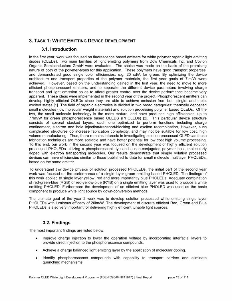
Section 3.6 gives details for the experimental conditions used including material providers. The section 3.7 reports improvement on injection properties by incorporation of interfacial layers, to assist direct electron and hole injection to the phosphorescence compound, and is based on our work on single emitting layer green PHOLEDs. Improvement in injection properties can reduce the operation voltage and thus can be used to achieve high luminous efficacy PHOLEDs. A similar approach (incorporation of hole injecting interfacial layer) was used to obtain a highly efficient yellow PHOLED, section 3.8. In the case of a red PHOLED the energy transfer approach from the green to the red phosphorescence emitter was used to obtain an efficient saturated pure red emitting PHOLED (section 3.9). The results reported for blue PHOLEDs, section 3.10, are obtained based on the modulation of the charge transport within the phosphorescence light emitting layer to achieve optimum charge balanced and optimization of the location of the exciton formation zone within the light emitting layer. The development of single layer white PHOLEDs are described in section 3.11 and show the importance of the compatibility and compositions of the selected materials used within the light emitting layer. The section 3.12 describes the development of a cool white source by phosphor down conversion. Work on light extraction methods is presented in section 3.13. The improvement in the phosphorescence emission rate due to incorporation of metal nano-particles in the interfaces of a green PHOLED is described in section 3.14. Finally, section 3.15 describes our suggestions for future work to exceed a 40 lm/W white emitting OLED and section 3.16 conclude our work.

Polymer OLED White Light Development Program – (#DE-FC26-04NT41947) | Final Report page 19 of 111
3.6. Experimental For PHOLEDs, the triplet energy levels of the materials involved are of crucial importance since luminescence quenching effects are likely to occur and deteriorate the device efficiency. High band-gap host materials with higher triplet energy than that of the phosphorescence dye are needed to minimize quenching. In particular poly(N-vinylcarbazole) (PVK) polymer has been shown to provide adequate confinement of the triplet excited state in the guest molecules and thus reducing luminescence quenching effects [9,10]. The non conjugated polymer PVK was used as a host for all the PHOLEDs reported in this report. The phosphorescence emitters and the Poly(9,9-dioctyl-fluorene-co-N-(4-butylphenyl)-diphenylamine) (TFB) used as an interfacial layer for green and yellow PHOLEDs were purchased from American Dye Sources. Poly(3,4-ethylenedioxy thiophene) doped with poly(styrene sulfonate) (PEDOT:PSS) used for buffer layer was purchased from H. C. Starck. PVK, N,N’-diphenyl-N-N’-(bis(3-methylphenyl)-[1,1-biphenyl]-4-4’-diamine (TPD), tri(p-tolyl) amine(TPTA) and 2-(4-biphenyllyl)-5-(4-tert-butylphenyl)-1,3,4-oxadiazole (PBD) were purchased from Sigma-Aldrich. The 1,3,4-oxadiazole, 2,2'-(1,3-phenylene)bis(5-(4-(1,1-dimethylethyl)phenyl) (OXD-7) was provided by Sensient. All the materials were used without any further purification. The gold nanoparticles with size of 1-10 nm dispersed in toluene solution were purchased from Mellorium Technologies. The concentration of the nano-particles used was in the range of 1.2 percent by weight.
The light emitting layer consists of a PVK host, blended with phosphorescence emitter/s, electron (PBD or OXD-7) and hole transporting molecules (TPD or TPTA). The emitting layer is then sandwiched between two injecting electrodes. The anode consists of indium-tin-oxide (ITO)/glass substrates pre-coated with PEDOT:PSS buffer layer. Prior to spin coating with the PEDOT:PSS buffer layer, the ITO was pre-cleaned and UV ozone treated. Then a 60 nm PEDOT:PSS layer was spin coated onto the ITO, and baked in a nitrogen environment at 200 ˚C for 30 min. The light emitting solution was prepared in chlorobenzene and spin coated on top of PEDOT:PSS layer inside a glove box to obtain a layer thickness of 70 nm. The light emitting layer was then annealed at 80 C for 30 min. The samples were then transferred into a thermal evaporator for cathode deposition. A typical cathode consist of CsF (1 nm) and aluminum (200nm) deposited at a typical pressure of 10-6 mbar. Incorporation of CsF has been reported to strongly improve electron injection [3]. Following evaporation, the devices were encapsulated with a glass lid and getter. For the green PHOLED TFB and PBD were used as interfacial layers between PEDOT:PSS and the light emitting layer. Spin coating from toluene solution at 2000 rpm/60 sec and baking at 130 C for 10 min produces a layer thickness of around 10 nm. To achieve an interfacial layer TFB and prevent mixing of the TFB with the light emitting layer, a toluene wash step was introduced prior to spin coating the emitting layer.
The PBD interfacial layer was thermally evaporated on top of the light emitting layer (LEP). The thickness for both hole and electron injecting interfacial layers were ≤ 3 nm. Incorporation of gold nano-particles into the device structure, was performed by spin-coating gold nano-particles dispersed in toluene at 1000 rpm for 30 seconds on top of the PEDOT:PSS buffer layer.
3.7. Green PHOLEDs Recently Yang, et al developed a single layer highly efficient PHOLED by using Tris(2-4(4-toltyl)phenylpyridine)iridium (Ir(mppy)3) doped into a PVK polymer host. The PVK: Ir(mppy)3 matrix was co-doped with PBD and TPD as the electron and hole transporting moieties respectively [11]. Incorporation of small molecules (molecular doping) into the phosphorescence emissive region was used to achieve a charge balanced state within the light emitting layer. Devices with luminous efficacy up to 24 lm/W at efficiencies exceeding 30 cd/A were reported [11]. During this year, we improved on this result by focusing on the device injection properties.

Polymer OLED White Light Development Program – (#DE-FC26-04NT41947) | Final Report page 20 of 111
3.7.1. Improving Hole Injection Properties:
A polymer based TFB interfacial layer was incorporated between the PEDOT:PSS layer and the light emitting layer to improve hole injection properties. The device architectures studied are described as follows. The control device is based on ITO/ CH8000 PEDOT:PSS / LEP / CsF / Al. To investigate the effect of the interfacial layer on the hole injection properties of the device, a TFB interfacial layer was inserted between the PEDOT:PSS and the LEP layer (ITO/ CH8000 PEDOT:PSS / Interfacial TFB / LEP /CsF/Al). The LEP composition was [61% PVK + 24% PBD + 9% TPD + 6% Ir(mppy)3]. The concentrations are given by weight.
TFB is particularly suitable for interfacial layer in green electrophosphorescence devices since its HOMO level is aligned with the HOMO level of TPD and Ir(mppy)3 at around 5.4 eV, as shown in Figure 3.5. We discuss this point further later in the text.
Figure 3.5: The HOMO and LUMO energy levels of TFB used for interfacial layers and Ir(mppy)3, PVK, TPD, PBD components of the LEP compared to the work function of PEDOT:PSS (all referenced with respect to vacuum). The vector in the scheme indicates the direct injection from the TFB interfacial layer into Ir(mppy)3 phosphorescence organo-metallic compound within the LEP.
Figure 3.6 shows the current density - voltage (J-V) properties (left plot) and the luminance-voltage properties (right plot) of the devices under study. From the J-V characteristics, it is clear that the current density is much larger for the device with an interfacial layer compared to the control device. In J-V measurements, the cause of the increase in the current density cannot be distinguished between injection and bulk transport properties. In fact, quite often both injection and transport contributes to it. In this case, however, we have shown elsewhere that the ultra-thin TFB interfacial layer does not affect the bulk transport properties. Consequently, the improvement in the current density is due to improved hole injection.
PEDOT:PSS
-5.1 eV
HOMO
TFB
-5.3 eV
PVK
-5.4 eV
TPD
PBD
-6.2 eV
-2.4 eV
-2.2 eV
LUMO
CsF/Al
Ir(mppy)3
-5.5 eV
-2.3 eV
LEP
-2.4 eV

Polymer OLED White Light Development Program – (#DE-FC26-04NT41947) | Final Report page 21 of 111
0 2 4 6 80
5
10
15
20
Control deviceTFB interfacial layer
Cur
rent
den
sity
(mA
/cm
2 )
Voltage (V)
0 1 2 3 4 5 6 7 8 9
2,000
4,000
6,000
8,000
Control device TFB interfacial layer
Lum
inan
ce (c
d/m
2 )
Voltage (V) Figure 3.6: Left plot: Current density-voltage characteristics of the solution processed electrophosphorescence OLEDs under study. Right plot: Luminance-voltage characteristics of the solution processed electrophosphorescence OLEDs under study. The control device is represented with open squares, the devices incorporating a TFB and PFO interfacial layer between PEDOT:PPS represented with solid squares and solid circles respectively. For all cases the light emitting layer contains [61% PVK + 24% PBD + 9% TPD + 6% Ir(mppy)3].
Further proof for the improvement in hole injection by incorporation of TFB interfacial layer can be seen in the luminance-voltage properties of the devices shown in the right plot of Figure 3.6. The luminance of the device with the interfacial layer is higher through the whole voltage range compared to the control device, indicating a lower driving voltage for devices with an interfacial layer. This is another indication that the TFB interfacial layer improves hole injection properties. The increase in device current and luminance observed with interfacial TFB layer is attributed to the matching of HOMO levels for hole injection from the interfacial layer into the LEP.
Figure 3.7, left plot shows the efficiency versus current density and the luminous efficacy versus current density (right plot) for the devices under study. The peak luminous efficacy (PCE) of the control device was 30 lm/W with an efficiency reaching 40 cd/A.
Finally devices with TFB interfacial layer show the highest PCE of 38 lm/W at device efficiencies exceeding 45 cd/A. The PCE achieved by incorporating TFB interfacial layer into the device architecture can be as high as 41 lm/W at luminescence efficiencies reaching 50 cd/A. This indicates that incorporation of the TFB interfacial layer can be used to achieve high efficiency PHOLED devices.

Polymer OLED White Light Development Program – (#DE-FC26-04NT41947) | Final Report page 22 of 111
0.01 0.1 1 100
10
20
30
40
50
Control device TFB interfacial layer
Lum
inan
ce e
ffic
ienc
y(cd
/A)
Current density (mA/cm2)
0.01 0.1 10
5
10
15
20
25
30
35
40
Control device TFB interfacial layer
Lum
inou
s eff
icac
y (lm
/W)
Current density (mA/cm2) Figure 3.7: Left plot- Luminance efficiency-current density characteristics of the solution processed electrophosphorescence OLEDs under study. Right plot: Luminous efficacy- current density characteristics of the solution processed electrophosphorescence OLEDs under study. The control device is represented with open squares, the devices incorporating a TFB and PFO interfacial layer between PEDOT:PPS represented with solid squares and solid circles respectively. For all cases the light emitting layer contains [61% PVK + 24% PBD + 9% TPD + 6% Ir(mppy)3].
Due to their similar HOMO levels, the TFB interfacial layer acts as a bridge for efficient hole injection into Ir(mppy)3 dye and TPD. The present results indicate that direct injection into the HOMO level of the phosphorescence organo-metallic compound is of high importance to obtain an efficient PHOLED. It should be noted here that the triplet energy levels of TFB are in the range of 2.2-2.3 eV, much lower than the triplet energy level estimated from the peak photoluminescence emission maximum of Ir(mppy)3 at 2.44 eV. Thus, one might expect that TFB can quench the light emission of the PHOLED [12,13]. In this case, quenching effects were not seen because the improved hole injection resulted in the moving of the recombination zone away from the anode.
In summary, incorporation of a TFB interfacial layer (with a HOMO energy level similar to that of the phosphorescence dye used within the LEP) between the PEDOT:PSS hole transporting layer and LEP can be used to assist direct hole injection into the phosphorescence compound without introducing additional strong luminance quenching effects, independent of the triplet energy levels of the materials involved. By introducing TFB interfacial layer into Ir(mppy)3/PVK/TPD/PBD solution processed PHOLED the driving voltage was reduced and a high PCE was achieved. The same technique can be applied to fluorescence based OLEDs, where the interfacial layer should be chosen such that the HOMO energy level of the interfacial layer lies between the HOMO energy level of the light emitting layer and the work function of the anode [14].
3.7.2. Improving Electron Injection
Further improvement in the device performance was achieved by improving electron injection properties thru the use of a small molecule electron injecting interfacial layer deposited on the cathode side of the device. The device architectures studied are described as follows. The control device is again based on ITO/ CH8000 PEDOT:PSS / LEP / CsF/Al. First improved device incorporates a PBD interfacial layer between the LEP layer and the cathode; ITO/ CH8000 PEDOT:PSS / LEP / PBD / CsF/Al. Second device architecture incorporates both TFB and PBD interfacial layers; ITO/ CH8000 PEDOT:PSS / TFB/ LEP / PBD / CsF/Al. The LEP for all the devices studied contains [61% PVK + 24% PBD + 9% TPD + 6% Ir(mppy)3]. The concentrations are given by weight. Figure 4 shows the device architecture incorporating the interfacial layers and the HOMO and LUMO energetic levels of the materials involved, as reported in the literature.

Polymer OLED White Light Development Program – (#DE-FC26-04NT41947) | Final Report page 23 of 111
Figure 3.8: The device architecture for optimized charge injection. Incorporating an electron (PBD) and hole (TFB) interfacial layers. The LUMO energy levels of PBD and the HOMO energy level of TFB are similar to that of the Ir(mppy)3 phosphorescence compound. The arrows in the scheme indicates the electron/hole injection from the PBD/TFB interfacial layers into Ir(mppy)3 phosphorescence compound.
An important point to draw from Figure 3.8 is that the LUMO level of PBD is well aligned to the LUMO level of Ir(mppy)3 and PBD in the LEP. The same is true for the HOMO level of TFB being aligned to the HOMO level of TPD and Ir(mppy)3. This good alignment of energy levels are important to facilitate carrier injection into Ir(mppy)3. Figure 3.9 upper plot shows the luminance efficiency versus current density and the lower plot shows the luminous efficacy versus current density for the devices under study. The peak luminous efficacy of the control device was 29 lm/W with a luminance efficiency reaching 40 cd/A. Devices with PBD interfacial layer show an improvement in the device performance, with luminous efficacy of 35 lm/W at luminance efficiencies exceeding 45 cd/A. Since the molecularly doped LEP is well charge balanced, incorporation of thicker electron transporting layers (6-10 nm) with hole blocking properties did not improve device efficiency [15]. When both PBD and TFB interfacial layers were used, the highest peak luminous efficacy of 50 lm/W with luminance efficiencies reaching 55 cd/A was achieved. This incorporation of interfacial layers can alternatively be described as a method of conditioning interfaces within organic electronic devices. As noted above, the interfacial layers act as a bridge for efficient electron/hole injection into the Ir(mppy)3 phosphorescent compound. This result indicates that though the control device is charge balanced, efficiencies can still be improved by increasing the number of carriers injected.
0.01 0.1 1 1020
30
40
50
60
Control Device PBD interfacial layer PBD and TFB interfacial layers
Lum
inan
ce e
ffic
ienc
y (c
d/A
)
Current density (mA/cm2)
0.01 0.1 1 10
0
10
20
30
40
50
Control DevicePBD interfacial layer PBD and TFB interfacial layers
Lum
inou
s eff
icac
y (lm
/W)
Current density (mA/cm2) Figure 3.9: Left plot: Luminance efficiency-current density characteristics Right plot: luminous efficacy- current density characteristics of the PHOLEDs under study. The control device is represented with open squares, the devices incorporating a PBD electron injecting layer represented with solid circles and the devices incorporating both PBD and TPD electron and hole injecting layers respectively represented with solid squares and solid circles respectively.
PEDOT:PS
HOMO
TFB
-5.3 eV
LEP
-5.4 eV
-2.4 eV
LUMO CsF/Al
Ir(mppy)3
PBD
-2.4 eV
h h
e e

Polymer OLED White Light Development Program – (#DE-FC26-04NT41947) | Final Report page 24 of 111
These results show that complicated multilayer PHOLED structures may not be necessary to obtain good efficiencies. Even when incorporation of thick transport/blocking layers into these complicated multilayer structures improve the luminance efficiency, the cost in operating voltage increase may be too high. We have demonstrated here that the increase in efficiency can be achieved even with simple structures that control charge balance and injection.
In summary, we have described a novel device architecture incorporating hole injecting interfacial layer with its HOMO level aligning with that of the phosphorescent dyes and the electron injecting interfacial layer with its LUMO level aligning to that of the phosphorescence dye. This hybrid device architecture can simplify the fabrication process, reduce the manufacture cost, and increase device efficiency while maintaining or even lowering the device operating voltage. By improving charge injection, a single emitting layer green PHOLED with luminous efficacy of 50lm/W, at luminance efficiency reaching 55cd/A, was achieved.
3.8. Yellow PHOLED Incorporation of TFB interfacial layer was also used to produce a highly efficient yellow PHOLED, ITO/ CH8000 PEDOT:PSS / Interfacial TFB / LEP /CsF/Al. The LEP contains [70% PVK + 15% PBD or 15 % OXD-7 + 15% yellow dyes]. The concentrations are given by weight. The yellow dye used here is Bis(2-(9,9-dihexylfluorenyl)-1-pyridine) (acetylacetonate) Iridium (III). The results indicate that the HOMO level of the yellow dye is in close alignment with the HOMO level of TFB. Thus, by improving hole injection properties we have obtain a yellow PHOLED (X=0.66, Y=0.49) with peak luminous efficacy of 23 lm/W at luminance efficiencies reaching 30 cd/A (Figure 3.10).
0.01 0.1 10
5
10
15
20
25
30
Yellow PHOLED
Current Density (mA/cm2)
Lum
inan
ce e
ffic
ienc
y (C
d/A
)
0
5
10
15
20
25
Luminous efficacy (lm
/W)
400 500 600 700 800
0.0
0.2
0.4
0.6
0.8
1.0
Nor
m E
L (a
.u)
Wavelength (nm)
X=0.50 Y=0.49
Figure 3.10: Luminance efficiency vs. current density and electroluminescence spectrum for the green PHOLED under study.
3.9. Red PHOLEDs By using a sensitizer green for red phosphorescence emission we have obtain a saturated red PHOLED (X=0.66, Y=0.33) with peak luminous efficiency of 7 lm/W at luminance efficiencies reaching 7 cd/A (Figure 3.11). The red dye used here is Bis(2-(2’-benzo-thienyl)pyridinato N,C3) (acetyl-acetonate) Iridium (III). The device structure is (ITO/ CH8000 PEDOT:PSS/ LEP /CsF/Al). The LEP contains [65% PVK + 15% PBD +15 % Ir(mppy)3+5 % red dye]. The concentrations are given by weight.

Polymer OLED White Light Development Program – (#DE-FC26-04NT41947) | Final Report page 25 of 111
0.01 0.1 10
2
4
6
8
10
Red PHOLED
Current Density (mA/cm2)
Lum
inan
ce e
ffic
ienc
y (C
d/A
)
0
2
4
6
8
10
Luminous efficacy (lm
/W)
400 500 600 700 800
0.0
0.2
0.4
0.6
0.8
1.0
Nor
m E
L (a
.u)
Wavelength (nm)
X=0.66 Y=0.33
Figure 3.11: Luminance efficiency vs. current density and electroluminescence spectrum for the red PHOLED under study.
3.10. Blue PHOLEDs The approach used for the control green PHOLED viz., molecularly doping a non-conjugated polymer host with phosphorescent emitters and small molecule transport moieties was similarly applied to the development of a blue PHOLED. By varying the composition of the LEP, two factors were identified to affect the device efficiency; 1) the charge (electron and hole) balance in the device, and 2) the location of the recombination zone within the LEP which affects the out-coupling of light from the device. Optimizing for both factors produce a luminous efficacy of 14 lm/W and luminance efficiency of 22 cd/A, comparable to efficiency values of small molecule systems that utilize the same phosphorescent emitter. This demonstrates that solution processed devices can have as high an efficiency as small molecule multilayer PHOLEDs in spite of their simple bi-layer device architecture, which is an important requirement in reducing manufacture cost for lighting applications
The LEP in these PHOLEDs are comprised of PVK as the hole transporting matrix, OXD-7 as the electron transporter and the blue phosphorescent dye Iridium (III)bis[(4,6-di-fluorophenyl)-pyridinato-N,C2]picolinate (Firpic). The amount of Firpic in the LEP is kept constant at 10% by weight, while the relative concentrations of PVK and OXD-7 are changed in order to vary the hole and electron transport within the LEP. The device structure and LEP composition with device labeling is shown in Figure 3.12.
Device A B C D
% OXD-7 0 10 20 30
0 2 4 6 8 100
5
10
15
20
25OXD- 7 content
0 % (A) 10 % (B) 20 % (C) 30 % (D) PVK device
Cur
rent
den
sity
(mA
/cm
2 )
Voltage (V) Figure 3.12: The table contains the device nomenclature based on the composition of the LEP. The schematic shows the device architecture along with the distance between the emission zone location (X) and the cathode. Also shown is the variation in current density vs. voltage for the different devices.

Polymer OLED White Light Development Program – (#DE-FC26-04NT41947) | Final Report page 26 of 111
The J-V data for the devices as a function of OXD-7 concentration is shown in
Figure 3.12. For comparison, the J-V data for a device with identical charge injecting electrodes where the LEP is comprised of neat PVK (henceforth referred to as the PVK device) is also shown. While PVK is a well known hole transporter, the presence of electrons in the neat PVK device using a CsF/Al cathode is confirmed, with pristine PVK-based electroluminescence with an intensity of 144 cd/m2 being observed at 10V. Compared to the PVK device, device A with only Firpic and no OXD-7 in the LEP has a very low current density. In order to explain this, we considered the values reported for the HOMO and LUMO of PVK and Firpic. The HOMO values reported for PVK and Firpic are relatively close to each other, suggesting that Firpic is unlikely to act as a hole trap. At the same time, the LUMO values for PVK (2.2 eV) and FIrpic (3.1 eV) indicate that FIrpic can act as a deep electron trap in a PVK matrix. Noting that the measured electron mobility of neat FIrpic is comparable to that of the other organic materials typically used as electron transporters in OLEDs, viz., Aluminum tris(8-hydroxyquinoline), Firpic would only act as an electron trap if it’s concentration is lower than the percolation threshold. The introduction of OXD-7 as an electron transporting moiety into the LEP for devices B-D results in an immediate rise in current density at any given voltage (Fig. 8). The rise in current density is most likely due to better electron transport within the LEP due to the presence of OXD-7. For all devices, the electroluminescence (EL) spectra are seen to be entirely due to FIrpic emission with CIE coordinates of (0.17, 0.37) at 1 mA/cm2 for device D.
In Figure 3.13, the luminous efficiency is plotted as a function of current density in the devices. Device efficiency is observed to rise with increasing OXD-7 concentration in the LEP between devices A-D. The efficiency of device D as a function of luminance is plotted as an inset within Figure 9 where peak device efficiencies of 22 cd/A and 14.5 lm/W are obtained at a luminance of 26 cd/m2. This compares favorably with published results for similar small molecule devices fabricated by high vacuum thin film coating methodology.8 Furthermore, the luminous efficiency of 20-22cd/A is observed to persist up to a device luminance as high as 800cd/m2. From the J-V data discussed above and optical simulation work described in Appendix A, it is evident that the improvement in device efficiency with increasing OXD-7 concentration is due to better electron transport in the device.
1 10 100 10000
5
10
15
20
25
10-6 10-5 10-4 10-3 10-2 10-1 100 101
5
10
15
20
25
Device A B C D
Current density (mA/cm2)
Lum
inan
ce e
ffic
ienc
y (c
d/A
)
cd/
A, l
m/W
Luminance (cd/m2)
cd/A lm/W
Figure 3.13: Luminance efficiency (cd/A) versus current density for devices with varying OXD-7 concentration in the light emitting spin coated layer. The inset shows cd/A and luminous efficacy (lm/W) data for device D plotted against of device luminance (cd/m2). Axes should be labeled the same way in all figures.

Polymer OLED White Light Development Program – (#DE-FC26-04NT41947) | Final Report page 27 of 111
The performance of the blue PHOLED was further improved by incorporating a new suitable hole transporting molecule named tri(p-tolyl) amine (TPTA) to achieve better charge balance. A blue PHOLED with peak luminous efficacy of 14 lm/W at luminance efficiencies reaching 25 cd/A was achieved (Figure 3.14). The device structure is (ITO/ CH8000 PEDOT:PSS/ LEP /CsF/Al). The LEP contains [60% PVK + 6 % TPTA+4 % Firpic+30 % OXD-7]. The concentrations are given by weight.
0.01 0.1 10
5
10
15
20
25
Current density (mA/cm2)
Lum
inan
ce e
ffic
ienc
y (C
d/A
)
-2
0
2
4
6
8
10
12
14
Luminous efficacy (lm
/W)
Figure 3.14: Luminance efficiency (cd/A) and luminous efficacy (lm/W) data versus current density for the blue PHOLEDs incorporating TPTA.
In conclusion, a simple approach to harvest triplets and singlets for blue electrophosphorescent devices was demonstrated. The results are obtained based on the judicious choice of charge injecting contacts, the modulation of the charge transport within the LEP and optimization of the location of the exciton formation zone within the light emitting layer. However, challenges such as the robustness of the device and the coating uniformity of large area panels remain. In this regard, the purity and the blend nature of the materials are two factors that need to be addressed in future work.
3.11. Single layer White PHOLEDs The development of an efficient blue PHOLED as described before further enabled the fabrication of white-emitting solution processed PHOLEDs, where the basic device architecture is comprised of ITO/ PEDOT/ LEP/ Cathode. The challenges mentioned above for the blue PHOLED, also apply to these white PHOLEDs.
3.11.1. Single layer RGB White PHOLEDs
In the first phase of developing a white emitting device, the emitters used for the optimized red, green and blue devices were utilized. The basic bi-layer device architecture utilized for the high efficiency blue PHOLED reported above was maintained, with the emitters in the LEP composed of 10% blue phosphorescent dye (Firpic), 0.05% green phosphorescent dye Ir(mppy)3 and 0.1% red phosphorescent dye bis(2-(2’-benzo-thienyl)pyridinato N,C
3)(acetyl-acetonate) Iridium(III). The device luminous efficacy
obtained was 16 lm/W. The efficiency was further improved to 20 lm/W and 27 cd/A using a light out-coupling foil. Thus the target of obtaining 20 lm/W solution processed white emitting devices was achieved (Figure 3.15). The emission spectrum of the device corresponded to a cool white color with CIE coordinates of (0.29, 0.43).

Polymer OLED White Light Development Program – (#DE-FC26-04NT41947) | Final Report page 28 of 111
10-3 10-2 10-1 100 1010
10
20
30
40
50
60
No Light Outcoupling With Light Outcoupling
Current density (mA/cm2)
Lum
inan
ce e
ffic
ienc
y (c
d/A
)
0
5
10
15
20
Luminous efficacy (lm
/W)
Figure 3.15: 20 lm/W single emitting layer cool white phosphorescence device.
In order to further improve the color coordinates of the device, and more importantly the Color Rendering Index (CRI), EL spectral simulations performed with the phosphorescent dyes available to us indicated that a higher CRI can be obtained if the green dye is replaced by our yellow dye.
3.11.2. Single Layer RYB White PHOLEDs
The base blue LEP is comprised of 60% PVK (host and hole transport), 30% OXD-7 (electron transport) and 10% Firpic (blue emitter).5 To this base LEP composition, a yellow phosphorescent dye- Bis (2-(9,9-dihexylfluorenyl)-1-pyridine) (acetylacetonate) Iridium(III) and a red phosphorescent dye bis(2-(2’-benzo-thienyl)pyridinato N,C
3)(acetyl-acetonate) Iridium(III) are added in varying concentrations, as given in
Table 2.
Table 3.3: Performance of the different devices as a function of the dye concentrations in the LEP. The large improvement in luminous efficacy (Devices A, B, E) is not only due to the better overlap of the emission spectrum of the yellow dye with the Photopic response of the eye, but also due to improved device quantum efficiency, as indicated in the Table. The addition of the red dye reduces both the quantum efficiency as well as the luminous efficacy.
Luminous Efficacy (lm/W) Device % Yellow dye,
% Red dye Peak @ 100 cd/m2
Ext. Quantum Efficiency (%)
CIE (x, y)
A Y(0.0) R(0.0) 14 12 9.5 0.17, 0.37
B Y(0.1) R(0.0) 24 17 12.2 0.30, 0.45
C Y(0.1) R(0.1) 18 15 11.3 0.33, 0.43
D Y(0.1) R(0.3) 15 10 10.1 0.43, 0.42
E Y(0.2) R(0.0) 28 22 15.2 0.35, 0.47
F Y(0.2) R(0.1) 20 16 12.6 0.41, 0.46
G Y(0.2) R(0.2) 18 13 11.4 0.42, 0.46

Polymer OLED White Light Development Program – (#DE-FC26-04NT41947) | Final Report page 29 of 111
400 450 500 550 600 650 700 750
B- Y(0.1) R(0.0) C- Y(0.1) R(0.1) D- Y(0.1) R(0.3) E- Y(0.2) R(0.0) F- Y(0.2) R(0.1) G- Y(0.2) R(0.2)
Wavelength (nm) Figure 3.16: Electroluminescence spectra of devices reported in this study. The spectra shaded grey are for devices which contain 0.1% of the yellow dye while the un-shaded spectra are for devices with 0.2% yellow dye.
Figure 3.16 shows the EL spectra of the devices containing yellow and red dyes at a fixed current density of 0.3 mA/cm2, normalized with respect to the area under the curve of each spectrum. The addition of the yellow dye increases the contribution to the emission at 550nm as determined from EL spectra for devices B and E. At the same time it is interesting to note the effect of increasing red dye concentration for the two yellow dye concentrations considered. While in all cases there is an increase in the EL intensity at 614nm corresponding to the peak emission from the red dye, there is a clear difference seen in the extent to which the blue emission is reduced at the expense of the red emission for devices B-D and devices E-G. Analysis of the EL spectra by de-convolution of the individual emitting components enabled us to draw the conclusion that direct exciton formation on the red dye was circumventing the usual mechanism of step-wise transfer of the excitons. This is an important result as it indicates that careful engineering of the energy levels of the red dye can prevent trapping related limitations on the luminous efficacy of the devices.
Figure 3.17 shows the luminous efficacy of device D as a function of current density. The device has a peak luminous efficacy of 15 lm/W and a color rendering index (CRI) of 87 (highlighted in table 2). On the CIE diagram, the color co-ordinates of device D place it very close to those of Illuminant A, which is a standard simulating an incandescent bulb. While the peak luminous efficacy is lower than that reported for small molecule multilayer devices, it is evident that the utilization of direct injection to the dye molecules can enable losses due to multiple band gap materials in a single layer to be minimized. Furthermore, we note that device D has a very high red component in the spectrum which also contributes to a warmer white. Further optimization to obtain a cooler white with less red and yellow dye in the LEP along with optimization of charge balance by tuning the OXD-7 concentration can further improve device performance. The use of interfacial layers reported above can also enable a further lowering of the operating voltage.

Polymer OLED White Light Development Program – (#DE-FC26-04NT41947) | Final Report page 30 of 111
10-3 10-2 10-1 100 101
0
5
10
15
20
Single Layer White
Current density (mA/cm2)
Lum
inou
s eff
icac
y (lm
/W)
Figure 3.17: Luminous efficacy (lm/W) performance of device D with a high CRI of 87.
3.12. Generation of White Light by the Means of Down-conversion White light emitting OLEDs can be generated by four approaches, schematically shown in Figure 3.18.
1. A single white emitting stack where the white emission is achieved by using a combination of different emissive components providing red, green and blue light from a single emitting layer. This device architecture offers easy processing but it is not easy to tune the color without affecting device performance.
2. A vertical red-green-blue (RGB) stack where the output spectrum of such a device is determined by the three light emitting components. This device architecture leads to color homogeneity over the active area but relies on complex processing methods.
3. A horizontal RGB stack where the output spectrum of a horizontal stack can be changed while operating the device when addressing the patterns separately. Current methods to manufacture a device in this way rely on sequential inkjet printing and patterning of the R, G and B emitting polymers. For all the above mentioned methods, color stability is difficult to be achieved due to different lifetime aging rates of the emitters involved.
4. A single color emitting OLED in combination with a down-conversion layer. This approach can be implemented by easy fabrication techniques and can provide better color stability as the aging rate is determined by only one emitter. White light emitting devices by the means of luminescence conversion based on an inorganic blue light emitting LED and down-conversion are widely used in existing LED products. Duggal et al. were the first to implement the idea to the field of OLEDs generating white light by combining a blue OLED with a down-conversion phosphor system [16,17]. Based on this approach an illumination quality lighting panel with an efficacy of 15 lm/W at 1000 cd/m2 was demonstrated.

Polymer OLED White Light Development Program – (#DE-FC26-04NT41947) | Final Report page 31 of 111
Below, two white light emitting devices based on luminescence conversion are presented:
Figure 3.18: Schemes of the 4 general approaches to generate white light based on organic light emitting devices.
3.12.1. Cool white light emitting device based on blue PHOLED
The efficiency of a white source developed by down-conversion method is determined by the underlying blue diode. As discussed in section 3.10 a highly efficient single-layer blue PHOLED with peak luminous efficacy of 14 lm/W at luminance efficiency reaching 22 cd/A at a luminance of 26 cd/m2 had been obtained. The CIE-coordinates of the blue emission are x = 0.17 and y = 0.37. This PHOLED will be used to demonstrate the down-conversion approach.
Simulations using the EL spectra of the blue PHOLED were performed to screen for phosphors that would be suitable to generate white light. A few phosphors were identified, but the one chosen was based on a nitridosilicate phosphor ([Sr,Ba,Ca]2Si5N8:Eu2+) [18,19]. The phosphor material is an internal product of OSRAM with a quantum yield of about 90 % of typical YAG:Ce. Figure 3.19 shows the excitation spectrum and the emission spectrum of the phosphor used in our experiment. As can be seen from the excitation and emission spectra, the phosphor will absorb a fraction of the photons emitted by the blue PHOLED and reemit them at wavelengths corresponding to the orange range of the visible spectrum. The resulting output spectrum of the device is the superposition of non-absorbed blue light and phosphor re-emission.

Polymer OLED White Light Development Program – (#DE-FC26-04NT41947) | Final Report page 32 of 111
200 300 400 5000
20
40
60
80
100
500 600 7000.0
0.2
0.4
0.6
0.8
1.0
emis
sion
[%]
excitation wavelength (nm)
inte
nsity
(nor
m.)
wavelength [nm]
Figure 3.19: Excitation and emission spectrum of the nitridosilicate phosphor used in the down-conversion layer.
Using a masticator, the phosphor particles were thoroughly dispersed in a silicone matrix (refractive index 1.47), in order to prevent aggregation quenching. This mixture was then applied on the substrate using the doctor blade technique. The down-conversion layer was cured at 70 C for 24 h. The thickness of the cured layer was 90 micrometers as measured by profilometry.
The photo in Figure 3.20 shows the white source developed by down-converting our blue PHOLED with the OSRAM phosphor. The graph in Figure 16 shows the normalized output spectrum of the device, and the corresponding C.I.E. coordinates of this cool white light source (x= 0.26, y = 0.40). By down-converting a blue PHOLED with efficiencies of 14 lm/W and 22 cd/A with an OSRAM phosphor, a highly efficient white light emitting source with luminous efficacy of 25 lm/W at luminance efficiency reaching 39 cd/A was obtained. This translates into a conversion efficiency of 180%.
400 450 500 550 600 650 700 7500.0
0.2
0.4
0.6
0.8
1.0
CIE x/y = 0.26/0.40
inte
nsity
(nor
m.)
wavelength [nm]
measurement model
Figure 3.20: Normalized output spectrum of the white light emitting down-conversion device. The spectrum was fitted according a simple down-conversion model, in order to calculate the expected efficiency of the device without consideration of light extraction enhancement. The picture shows the white light emitting device.

Polymer OLED White Light Development Program – (#DE-FC26-04NT41947) | Final Report page 33 of 111
This value is much higher than that predicted by the down-conversion model previously proposed by Duggal et al [16]. The model takes into account the absorption and emission spectra of the phosphor, a self-absorption correction of the down-conversion layer, the EL-spectrum of the blue PHOLED and the quantum yield of the phosphor. The effective optical path length of the light in the phosphor layer is used as the only fitting parameter and was varied in order to obtain the best fit of the output spectrum. The calculations for the expected efficiency include parameters related to the sensitivity of the human eye and the Stokes shift between the energy of absorbed and reemitted photons. After determining the fitting parameter, a factor that relates the efficiency of the blue PHOLED and the efficiency of the resultant white device is obtained. This factor, we define as the conversion efficiency, such that a conversion efficiency of 50 % will yield a white device that is half as efficient as the original blue PHOLED. The calculated conversion efficiency is only 94%, far lower than the 180% seen experimentally. This difference may be attributed to light extraction effects due to light scattering by the phosphor particles, which is not considered by the model.
Volumetric light scattering due to particles embedded in a coating on the substrate surface has been reported to enhance light extraction [20]. The introduction of volumetric scattering mechanisms due to ZrO2 particles embedded in a coating on the substrate surface has been reported to increase the output of OLEDs by as much as 40%. However, the light extraction value that is reported is still much lower than what we observe.
The difference in the values may be caused by the fact that our phosphors do not only scatter, but also get excited and emit. In order to separate the difference between light extraction enhancement due to volumetric light scattering and enhancement due to absorption/re-emission mechanism of our OSRAM phosphor, the efficiency enhancement of an orange light emitting OLED due to the same down-conversion layer described above was compared to the enhancement of the blue PHOLED in our white device. The conversion layer in the orange OLED functions as a volumetric scattering layer as the phosphor does not absorb in the orange. To ensure a fair comparison, the extraction efficiency based on the fraction of light that is lost in the substrate for both OLEDs when uncoated has to be considered.
The emission intensity of the uncoated orange OLED and of the uncoated blue PHOLED was measured with a Si photodiode. The distance between the Si photodiode and the OLED substrate’s surface was kept at <0.5 mm. Measurements were carried out alternatively with an air gap and an optical gel whose refractive index was 1.56 [21]. When the air gap was filled with gel, total internal reflection at the glass/air interface disappeared, enabling the emitted light of the external and substrate wave-guided modes to be measured by the Si photodiode simultaneously. For the orange and for the blue PHOLED, about 50 % of the light, which is generated in the device stack and coupled into the substrate, is extracted to air. After applying the same down-conversion layer on the substrate surface of the orange light emitting OLED, its light output was measured again. The output of the orange OLED was increased by 30%, which is lower than the 88 % seen with the blue PHOLED. This confirms that pure volumetric scattering cannot account for the light extraction enhancement seen in our white device. This difference is due to the phosphor particles being excited and re-emit. Re-emission by the phosphor particles is isotropic, while the radiation patterns of scattering media is not. Furthermore, previous work has shown a dependence of the light extraction enhancement on the radiation pattern of the particles [20]. Thus, in the case of the down-conversion layer presented here, we propose, that a more isotropic radiation pattern of the particles leads to a higher light extraction enhancement due to the excitation/reemission mechanism.
In conclusion, it has been demonstrated a highly efficient white light emitting device based on a blue PHOLED down-converted with an appropriate phosphor layer. Such a device can be fabricated cheaply, due to the solution based production process of the PHOLED and due to the simple application technique of the down-conversion layer. Extraordinary enhancement of the device’s external light output was observed, resulting in a 25 lm/W white light emitting diode performance. This strong enhancement has been attributed to the isotropic radiation pattern of the excited phosphor particles.

Polymer OLED White Light Development Program – (#DE-FC26-04NT41947) | Final Report page 34 of 111
3.12.2. Novel Approach to Generate Illumination Quality Light Based on Bluish-Green Emitting OLEDs
The basic disadvantage of approach 1 to generate white light (ref. to introduction of 3.12) is a lower efficiency due to electron trapping caused by the red organic emitter. The shortcoming of approach 4 is the blue emitter, which usually offers lower quantum efficiency compared to a green emitter.
Here we propose a novel approach, which eliminates the disadvantages of approach (1) and (4) but keeps theirs advantages. This approach makes use of a bluish green emitting OLED coated with a down-conversion layer. The down-conversion layer absorbs a part of the green light and emits red light. The advantages of this method are:
The device is based on a bluish green OLED, which possess a higher quantum efficiency than a blue OLED.
There is no red light emitting component, which might lead to electron trapping, in the EL-active part of the device. Thus a lower operating voltage of the device can be achieved. Color tuning almost always affects the efficiency.
Processing of the device is much easier than using approach 1, because there are only two EL-active components in the device (green and small amount of blue).
3.12.2.1. Example: White Light Emitting Device Based on a Bluish-Green Emitting PHOLED
The device is based on a bluish green emitting PHOLED. A down-conversion system is applied on the substrate surface. The system consists of two down conversion layers, which contain an orange and a red emitting perylene dye (Lumogen Red/Orange obtained by BASF fluorescence quantum yield = 95%) dissolved in a PMMA-matrix. The down-conversion system mainly absorbs the green light emitted by the PHOLED. Figure 3.21 shows the emission spectrum of the PHOLED, the absorption and reemission spectra of the fluorescent dyes and the resulting white spectrum. Based on the device performance achieved for the bluish green emitting PHOLED with luminous efficacy of 18 lm/W a peak efficiency of 13 lm/W can be achieved for the resulting white device (without light extraction enhancement). The CIE color coordinates are x/y = 0.40/0.40 (corresponding color temperature = 3750 K). The CRI of the light generated by the device is 77.

Polymer OLED White Light Development Program – (#DE-FC26-04NT41947) | Final Report page 35 of 111
400 500 600 7000.0
0.2
0.4
0.6
0.8
1.0
inte
nsity
(nor
m.)
wavelength (nm) 400 500 600 700
0.0
0.2
0.4
0.6
0.8
1.0
inte
nsity
(nor
m.)
wavelength (nm) (a) (b)
400 500 600 7000.0
0.2
0.4
0.6
0.8
1.0
0.0
0.2
0.4
0.6
0.8
1.0
Abs
orpt
ion
(nor
m.)
wavelength (nm)
Flu
ores
cenc
e (n
orm
.)
400 500 600 7000.0
0.2
0.4
0.6
0.8
1.0
0.0
0.2
0.4
0.6
0.8
1.0
Abs
orpt
ion
(nor
m.)
wavelength (nm)
Flu
ores
cenc
e (n
orm
.)
(c) (d) Figure 3.21: (a) EL-spectrum of bluish-green emitter. (b) Resulting output spectrum of the device. (c) Absorption and re-emission spectra of the orange perylene dye. (d) Absorption and re-emission spectra of the red perylene dye.
3.13. Light Extraction One evident drawback of OLEDs is still the low light out-coupling efficiency. The internal device efficiency is related to the rate of emission. The external device efficiency is determined by the fraction of light, which is generated in the device stack and extracted to air. The mismatch of the refractive index between air and the OLED reduces the light output due to poor extraction of generated light. Total internal reflection (TIR) into wave guiding modes and self absorption are two mechanisms responsible for this reduction.
Many approaches have been utilized to increase the out-coupling efficiency. These can be divided into six generic schemes:
(1) The patterning of polymer microlens array on the substrate surface, or placing a large size index matching hemispherical lens on top of the substrate.
(2) Introducing scattering effects at the substrate surface by means of techniques such as applying a transparent coating on the substrate with embedded small particles, or texturing the substrate surface.
(3) Incorporating the light emitting diode in a reflecting mesa structure.

Polymer OLED White Light Development Program – (#DE-FC26-04NT41947) | Final Report page 36 of 111
(4) Inserting an extremely low refractive index (n ≈ 1.03) silica aerogel porous layer between the ITO transparent anode and the glass substrate.
(5) Increasing light out-coupling efficiency by means of micro-cavity effects due to the double mirror structure of the organic light emitting device given by both electrodes and the organic layers embedded in between.
(6) Application of lateral periodic nano structures on the substrate leading to increase of light out-coupling through Bragg scattering.
Two studies were conducted, in order to develop a deeper understanding of light extraction. In the first study we investigated optical effects in the OLED micro-cavity due to change of the location of the emission zone as a result of improved charge balance. In the second study a general method to valuate light extraction enhancement due to substrate surface modification was developed.
3.13.1. Effect of Charge Balance and Micro-cavity Effects in Resultant Efficiency of OLEDs
The OLED stack is a micro-cavity albeit a weak one, due to the double mirror structure given by both electrodes and the organic layers embedded in between. The external and internal device efficiency is influenced by micro-cavity effects. Electrons and holes injected from the respective contacts recombine in the emission zone (EMZ) to form emissive excitons. Because these excitons are optically close to the highly reflective cathode, the rate and the direction of emission are strongly modified by optical interference effects. The internal device efficiency is related to the rate of emission. The external device efficiency is determined by the fraction of light, which is generated in the device stack and extracted to air. The mismatch of the refractive index between air and the OLED reduces the light output due to poor extraction of generated light. Total internal reflection (TIR) into wave guiding modes and self absorption are two mechanisms responsible for this reduction. As indicated in Figure 3.22 light emitted by the device can be classified into three modes: the external mode, the substrate wave-guided mode and the anode/organic wave-guided mode. Depending on the emission angle of the light to the substrate normal, the generated photons are out-coupled or wave-guided into the substrate and the active layers respectively.
device stack
substrate Θ
air
anode/organic wave guided mode
substrate wave guided mode
external mode
Figure 3.22: The external mode, the substrate wave-guided mode and the anode/organic wave-guided mode in an organic EL device. Dependent on the emission angle θ the generated photons are out-coupled or wave-guided.
The internal device efficiency of OLEDs can be increased by improving charge balance in OLED devices. At the same time a modification of charge balance leads to a change in the location of the emission zone (EMZ). The optical effects in the OLED micro-cavity are determined by the location of the EMZ. Thus the resultant change in device efficiency is a superposition of improved charge balance and optical effects.
This effect can be illustrated using the blue PHOLEDs discussed in section 3.10. A detailed description of the experimental procedures and treatment is given in Appendix B. Here, we will only summarize the results, represented graphically in Figure 3.23. By increasing the OXD-7 content of the LEP from device A to D, electron transport is enhanced. Since the PVK host is hole transporting, an increase in electron transport improves the charge balance of the device, and an increase in device efficiency is expected.

Polymer OLED White Light Development Program – (#DE-FC26-04NT41947) | Final Report page 37 of 111
From Figure 3.23, an increase in efficiency by a factor of 8.5 is recorded. Thru the use of optical simulation models, the optical effect due to the recombination zone movement in a micro-cavity was determined. For device D, the optical effect resulted in an improvement by a factor of 2. Consequently, the improvement due to charge balance is only 4.25X. Furthermore, as evident in Figure 3.23, the ratio of the optical and charge balance effect is not constant. This illustrates that even for an OLED which is considered to be a weak cavity, the optical effects can be significant, and cannot be ignored a priori and that care needs to be taken in interpreting device performance results. In the same vein, a general method that takes these effects into account in order to more accurately determine the effectiveness of light extraction techniques is presented in Appendix C.
0 10 20 30 400123456789
10
∆1
A DCB E
light
out
put (
norm
.)
OXD7 conc. [%]
+ = measured light output improvement due to cavity effect ∆2
Figure 3.23: The external light output of the devices used in this study normalized on the output of device A. The cross hatched area represents the efficiency improvement compared to device A due to the micro-cavity effect. The improvement in internal device efficiency is marked by the double ended arrows.
3.13.2. Brightness Enhancement Film
A Brightness Enhancement Film (BEF) prepared from 3M (Vikuiti BEF II 90/50) was evaluated for its effectiveness as a light extraction technique for our PHOLEDs using the technique described in Appendix C. The BEF film consists of an acrylic resin with prismatic features on its surface coated on a polyester substrate. The prism angle is 90° and the prism pitch is 50 µm. The BEF film was optically coupled to the glass substrate with optical laminating tape (3M No. 8141, n = 1.49).
Figure 3.24 shows the external light output of the devices before and after applying the BEF film as a function of the Alq3 thickness. It is observed that with increasing Alq3 thickness the light output in both cases (i.e., without and with the BEF film) decreases. However, the effect of light out-coupling enhancement due to the BEF film is increased. With the technique described in Appendix C, it was determined that with the BEF film, about 60 % of the light, which is coupled into the substrate, is extracted out of each modified device. Thus, the extraction efficiency of the BEF film was 60%.

Polymer OLED White Light Development Program – (#DE-FC26-04NT41947) | Final Report page 38 of 111
1 2 3 4 50.0
0.5
1.0
1.5 without BEF with BEF
30 7050100
Inte
nsity
(nor
m.)
Thickness of Alq3 layer [nm] Figure 3.24: Light output of the devices before and after applying the Brightness Enhancement Film. The intensities are normalized on the output of the light output of the device with an Alq-layer thickness of 10 nm. The error bars represent the standard deviations of the measured values.
3.14. Improving Emission Rate The use of metallic nano-particles in organic host materials to accelerate the emission rates has attracted interest from the research community [24, 26]. The acceleration of the radiative processes is achieved by the interaction of the light emitting species with surface plasmon resonances in the vicinity of metal nano-particles resulting in an improvement of efficiency for triplet emitters. In the case of fluorescence based OLEDs, improvement in efficiency is indirectly achieved when triplet non-radiative excited states are quenched, thus suppressing photo-oxidation and other singlet radiation quenching pathways [25].
However, direct incorporation of metal nano-particles into the active region or other layers within the OLED can have negative effects. For example, incorporation of a gold nano-particle even at low volume fraction of 3 x 10⁻⁵ within a light emitting fluorescence polymer layer introduces strong hole blocking effects and a large increase in operating voltage [27]. The metal nano-particles can also quench the excitons Forster-type energy transfer between the emitter and the metal nano-particle. Encasing nano-particles in organic capping molecules has been tried to achieve an optimum balance between quenching and acceleration of the radiative processes of the emissive states. A nearly two fold increase of luminance efficiency of slow phosphorescence (2,3,7,8,12,13,17,18-Octaethyl-21H,23H-porphine platinum (II) based OLEDs (around 10 microsecond emission lifetime) has been reported by blending into the PHOLED LEP thiol-capped gold nano-particles [26]. However accelerating the radiative properties of faster phosphorescence emitters such as the currently used Iridium based compounds with 1 microsecond emission lifetime, is not straightforward and capping of the metal nano-particles is not a well known procedure.
In this section, we summarize work on a novel method to introduce these metal nano-particles into the PHOLED while minimizing the adverse effects mentioned above. The detailed description of the work is presented in Appendix D. Gold nanoparticles with a diameter of 1-10nm were used as their optical absorption band overlaps with the energy level of the triplet excitons of our Ir(mppy)3 emitter. By conditioning the surface of the Pedot:PSS layer, and hence sandwiching the gold nanoparticles between the Pedot:PSS and LEP, we hope to minimize the adverse effects of the nanoparticles while making use of the rate acceleration effect. The efficiency of the PHOLED was increased by 33% from 27 cd/A to 36 cd/A (Figure 3.25). The strong enhancement in the luminance efficiency for the phosphorescence devices incorporating gold nano-particle in the interface between LEP and adjacent layers is a product of an increased radiative decay rate due to modification in the local density of states caused via an interaction of the phosphorescence emitter with the metal nano-particles surface plasmons [26,28].
Polymer OLED White Light Development Program – (#DE-FC26-04NT41947) | Final Report page 39 of 111
-200 0 200 400 600 800 1000 1200 1400-5
0
5
10
15
20
25
30
35
40
Lum
inan
ce e
ffic
ienc
y (c
d/A
)
Luminance (cd/m2)
Control Device Device with gold nanopartcles
Figure 3.25: Luminance efficiency-luminance characteristics of the phosphorescence OLEDs under study. The control device is represented with open squares, the devices incorporating gold nano-particles in the interface between buffer layer and LEP represented with solid squares.
3.15. Future Work: Strategy for 40 lm/W White Source The results presented above indicate that a 40 lm/W white PHOLED can be developed. This can be achieved by incorporation of suitable interfacial layers into white PHOLED structure (see section 3.7.1 and 3.7.2). A 66% improvement in the luminance efficacy of Green PHOLED was obtained by incorporation of interfacial layers to improve electron and hole injection and a similar concept can be applied to white PHOLEDs. Furthermore, doping at both electrode interfaces can further improve injection and thus further reduce the operation voltage, improving the luminous efficacy. Optimization of the processing conditions used to incorporate gold nano-particles in the interfaces of OLEDs can also be used to increase the luminance efficacy. Finally, challenges such as the robustness of the device and the coating uniformity of large area panels need to be addressed. The main approaches will focus on the purity of the material, and integration of a phosphorescent-emitting blend material into a single polymer.
3.16. Conclusions In conclusion we have demonstrated the parameters determining the device performance of PHOLEDs. By understanding the material and device physics of solution processed PHOLEDs we gain the knowledge of selecting the adequate combination of materials and device structures to developed highly efficient devices. We have developed green, yellow, blue and red PHOLEDs exhibited luminance efficacy of 50 lm/W, 23 lm/W, 14 lm/W and 7 lm/W respectively. Furthermore a cool white source by down conversion system with a luminous efficacy of 25 lm/W and a single white emitting layer light source with a luminous efficacy of 20 lm/W were demonstrated. To our knowledge the PHOLEDs device performances, for all the different emitting color presented here, are the highest reported in the literature by solution processed techniques and in several cases rivaling those of published multilayer small molecule PHOLEDs. In the field of general lighting the realization of high performance organic electronic devices, based on simple cost-effective fabrication procedures, will enable PHOLEDs to be major contributors in the quest to reduce energy consumption. The key challenge will be to transfer this high luminous efficacy from an R&D level to a large tile format.

Polymer OLED White Light Development Program – (#DE-FC26-04NT41947) | Final Report page 40 of 111
4. TASK 2: WHITE TILE DESIGN, FABRICATION, AND TEST
4.1. Summary Description The objective of this task was to explore different design possibilities and to optimize the uniformity, efficiency, and reliability of a large-area OLED lighting tiles. Additionally, this task was to optimize the device structure and processing conditions for working with the materials identified in Task 1. Finally, this task included the preparation of 6”x10” demonstration lighting panels which generated white light meeting the performance specifications for the project.
Objectives achieved during the year 1 of the project were:
• Completed the design of both a striped and uniform, single “pixel” design. • Transferred the process and materials from Task 1 into the Process Development Line for scale-
up. • Troubleshooting of design issues specifically related to this design. • Optimized the processing conditions for maximum efficiency, CRI, and uniformity. • Prepared tiles for use in the Year 1 demonstrators.
During the course of the year 2 the following major accomplishments were achieved:
• Refined the strategy of producing large-area panels to use smaller tiles. This was necessary due to the low yields of producing the original 2”x3” single pixel tile.
• Demonstrated the new strategy using an existing OSRAM design, not optimized for fill factor. • Produced white light panels comprised of a) white emitting single pixel tiles and b) individual red,
green and blue emitting single pixel tiles. • Redesigned the small tile to double the fill factor of the final panel (Polaris design). • Used the Polaris design to successfully demonstrate the scale up of a high efficiency
phosphorescent LEP process, transferred from Task 1.
4.2. Detailed Description
4.2.1. Tile Fabrication
All tiles produced for this task (as also described in Section 2.2) were made in the OLED Process Development Line in San Jose. The line is contained in a class 1000 cleanroom that is divided into individual bays based upon process type.
Incoming ITO-coated glass is first cleaned using brushes, high pressure DI water spray, and megasonic treatment in an SSEC Trillenium cassette-to-cassette cleaning tool. Once clean, the substrates go through a vapor priming step and are then coated with photoresist. The photoresist is exposed using a Karl Suss MA8 proximity mask aligner. Exposure is followed by development of the pattern, etching of the ITO, and stripping of the photoresist in standard batch wet sinks.
Following ITO patterning, the substrate is metallized using a Kurdex Corp. RF-sputtering system. Three metal layers are used to provide the contact metallization for addressing the tile. Photolithographic patterning of the metal layers is then done as described above. To complete this part of the processing, a sacrificial resist material is patterned on the perimeter of the tile to improve the integrity of the encapsulation seal.

Polymer OLED White Light Development Program – (#DE-FC26-04NT41947) | Final Report page 41 of 111
After all of the photolithographic pattering is complete, the tiles go through a final high pressure spray clean and are ready for application of the active polymer materials. Using RC-13 spincoaters from Karl Suss, the PEDOT:PSS and light-emitting polymer (LEP) layers are applied. Before the LEP is applied the PEDOT:PSS film is baked under vacuum at 200 °C. After applying the LEP it is baked to completely dry the film.
Laser patterning of the active polymer layers is necessary to open via holes for cathode contact and to clean the perimeter for encapsulation. This patterning is achieved using a Resonetics micromachining system with a Kr:F excimer laser operating at 248 nm.
The cathode metal is deposited on the substrate using thermal evaporation in an Ulvac Satella system. This tool is equipped with two deposition chambers, each having two temperature controlled crucibles for low work function metals and a wire-fed Al boat.
After cathode deposition, encapsulation of the substrate is performed in an MBraun nitrogen glove-box operating at less than 1 ppm water and oxygen. The process involves laminating the substrate glass to a cap glass which has an etched cavity for each tile. Absorbent getter materials are glued inside each cavity to protect the active materials from moisture that permeates through the adhesive over time. Finally, adhesive is dispensed around the perimeter of each tile, the two glass plates are aligned in a custom-built alignment and press fixture, and then cured by exposure to UV light.
The laminated plate is then scribed and broken into individual tiles using a Villa Precision Inc. scribing tool and broken manually.
4.2.2. Designs
The Year 2 deliverable for this task is to produce a lighting panel that is approximately 6”x10” in size. In the San Jose Process Development Line, processing is done on glass that is 200x200 mm. The original design, used for the Year 1 demonstrators, was for relatively large 2”x3” tiles. Using this design, six lighting tiles could be produced on each substrate (Figure 4.1)
Figure 4.1: 200 x 200 mm substrate with six Year 1 lighting tiles (left) and details of the layout of the tile (right).

Polymer OLED White Light Development Program – (#DE-FC26-04NT41947) | Final Report page 42 of 111
The original tile design utilized a striped pattern, i.e. light was emitted from 96 discrete lines. The reason for this design was to build in fault tolerance. If one line of the display shorted, it could be turned off and have only about a 1% effect on the tile performance as a whole.
However, even without defining the striped pattern, it was noticed that none of the tiles exhibited early pixel short failures. At that time, it was decided to pursue the uniform single “pixel” tile approach in order to simplify the design and improve the spin coating uniformity of the light emitting polymer. The risk of this approach was the formation of pixel shorts during extended operation and a task was undertaken to characterize this risk. The details of this study are reported later in this section (see Page 47).
After freezing the design for the single “pixel” approach, final optimization of the luminance uniformity began. It was found that tiles had a wavy non-uniformity that was eventually determined to form during the drying of the light emitting polymer layer. Experiments were conducted varying the drying parameters of this film and a condition was determined which minimizes the luminance non-uniformity (see Figure 4.2).
Figure 4.2: Wavy pattern in luminance due to non-uniformity in the light emitting polymer layer (left). Improved uniformity achieved by optimizing drying conditions (right).
The approach used for encapsulation involves the lamination of a “cap glass” to the active OLED substrate. This cap glass has a cavity to accommodate getter materials used to improve the shelf life of the tile. Our existing display process uses a cap glass that is 1.1 mm thick and has a cavity of 0.45 mm. Initial concerns about the possibility of the cap glass deflecting or breaking led us to design for a 2.0 mm thick cap glass with a cavity depth of 0.70 mm in order to provide better mechanical strength. It was found, however, that the thicker cap glass caused stress on the adhesive bond during the scribe and break process used to singulate the tiles.
In order to improve the process, two actions were taken. First, a photoresist layer was added to the seal area to improve the integrity of the bond during the singulation process. Second, 1.1 mm cap glass was obtained for trials. Using the thinner cap glass resulted in inward deflection in the center of the tile. In combination with inward deflection of the 0.7 mm substrate glass, the two pieces touch, resulting in shorting at the center of the tile.
For the final demonstrators, we have again used the 2.0 mm cap glass together with the photoresist adhesion layer. In this configuration, only the substrate glass deflects, but not enough to result in contact with the cap glass.
In spite of the improvements made to the uniformity and encapsulation process, these two issues still remained significant. With only six of the large area tiles on a substrate, the yield for producing high quality tiles was near zero. In order to improve yield, it was decided to use a smaller building tile (approximately 1.0”x1.1”). Using this size tile, there are 42 units on each substrate; thus greatly improving the yield.
In order to quickly prove the concept of assembling small tiles into a large-area panel, we used an existing design. In this design, the light emitting area of the tile was circular in shape and thus the fill factor of the tile was only 40%. Nonetheless, using a driving scheme developed in Task 4, we demonstrated that we could assemble 40 of these tiles in a 4x10 array without great difficulty.

Polymer OLED White Light Development Program – (#DE-FC26-04NT41947) | Final Report page 43 of 111
In order to improve the overall efficiency of the panel, we had to increase the fill factor of the individual tiles. In order to accomplish this, we converted the light emitting area to a more square shape and challenged our existing design rules. A key challenge in the success of the Polaris design was the decision to decrease the encapsulation seal width from our standard 1.8 mm to 1.0 mm. In doing so, we can minimize the non-emissive, “dead” area in the tile.
The layout of 42 tiles on our 200 mm substrate coupled with the details of the tile design is shown in Figure 4.3 (below). By using this Polaris design, the fill factor of the tile was increased to 66%.
Figure 4.3: Design for the 200 x 200 mm substrate with 42 Polaris lighting tiles (left) and detail of the layout of the tile (right).
4.2.3. White Emitter Process Development
During the first year of the program, we developed an optimized structure and process using a polymer from Covion, a division of Merck, resulting in an average efficiency of 6.0 lm/W and a CRI of 77 (see Figure 4.4). These conditions were used to prepare the Year 1 tiles for demonstration.
2.00
2.50
3.00
3.50
4.00
4.50
5.00
5.50
6.00
6.50
7.00
OLED Structure
lm/W
70.00
71.00
72.00
73.00
74.00
75.00
76.00
77.00
78.00
CR
I
lm/W at 100 mACRI
Figure 4.4: Efficiency and CRI as a function of OLED device structure.
Optimized structure

Polymer OLED White Light Development Program – (#DE-FC26-04NT41947) | Final Report page 44 of 111
During the course of the second year of the program, however, our materials suppliers were unable to provide materials whose performance surpassed that of the white polymer used in Year 1. A few materials from Covion were screened but were not found to be suitable replacements.
The lifetime of the materials evaluated during Year 2 also did not show any improvement. The lifetime of the panels produced in Year 2 will remain about 700 hours (Figure 4.5)
Figure 4.5: Lifetime of tiles from an initial luminance of 250 cd/m2. Tiles 1 and 3 developed shorts near the end of the test.
One of the deficiencies of the equipment used to produce these tiles is that the processing must be performed in air. We have shown in other experiments that the lifetime of the class of polymers used in this task is sensitive to air exposure during processing. Plans to install new equipment that would allow processing in nitrogen were delayed until October 2005, and were ultimately cancelled.
One of the targets in the second year for this task was to begin processing the phosphorescent materials developed in Task 1 on the Polaris design in the pilot line. The first and only such material that was processed was the green phosphorescent LEP. The ultimate performance of this material is only achieved when using a CsF cathode, as demonstrated in Task 1. However, due to process compatibility issues with other processes running in the pilot line, we were not able to use CsF and had to use LiF. The choice to first process the green material with LiF cathode was made to allow for a quick check of performance versus that obtained in Task 1 and to allow for some process debugging. Ultimately, the plan for year 2 was to introduce CsF into the pilot line and to process Polaris tiles using the best white phosphorescent emitter.
Task 1 results for the green phosphorescent LEP with LiF cathode showed a peak efficiency of about 13 lm/W versus 30 lm/W using a CsF cathode. For the Polaris devices, the peak efficiency obtained was about 14 lm/W (35 cd/A) (see Figure 4.6). These results compare very favorably with the Task 1 results for devices processed completely inside a nitrogen glovebox.
05
10152025303540
0 200 400 600 800
Lumninance (cd/m2)
cd/A
02468
10121416
0 2 4 6 8 10
Voltage (V)
lm/W
Figure 4.6: Efficiency performance of the green phosphorescent LEP on the Polaris design, fabricated in the pilot line (need to label the y-axes).
0
50
100
150
200
250
300
0 100 200 300 400 500 600 700 800
lifetime / hours
lum
inan
ce /
nits
plate 1plate 2plate 3

Polymer OLED White Light Development Program – (#DE-FC26-04NT41947) | Final Report page 45 of 111
In terms of lifetime performance, however, the performance of the Polaris tiles was much worse than the results obtained in Task 1. While the lifetime from 100 cd/m2 achieved in Task 1 was several hundred hours, the lifetime of the Polaris tiles was only about 5 hours. (See Figure 4.7)
50
60
70
80
90
100
110
0 100 200 300
Time (min)
Lum
inac
e (c
d/m
2 )
7.8
8
8.2
8.4
8.6
8.8
9
9.2
0 100 200 300
Time (min)
Volta
ge (V
)
Figure 4.7: Luminance decay (left) and voltage rise (right) for the green phosphorescent LEP fabricated in the Materials and Device Line.
As is the case with the fluorescent, conjugated white emitter, it is suspected that exposure to air during the processing of the phosphorescent material will seriously degrade lifetime performance. Again, if equipment designed to allow processing in nitrogen were used to produce devices, a much improved lifetime would have been expected.
4.2.4. Efficiency
The ultimate efficiency achieved by the tile is about 6 lm/W. This falls slightly short of the year 1 target value of 7 lm/W. Based upon the results from Task 1, this appears to be a limitation of the material, and is not determined by the design of the tile.
As discussed above, the original design used involved striping and we investigated the use of a diffusing film to help blur the stripes and make a more uniform light source. We found that these diffusing films also helped to extract light that gets trapped in the glass substrates by wave-guiding effects due to the significant change of the refractive index at the substrate-air-crossing.
The use of special brightness enhancing films (BEFs) resulted in widening or splitting of the light which is emitted by the individual stripes sources. The images of the individual stripes will run together or even overlap generating a more uniform lit area. For further applications, especially color-tunable lighting using alternating RGB striped tiles, this method could be applied to blend the three color components.
Figure 4.8: Diffusion effects of Brightness Enhancement Film.
With Diffuser
Without Diffuser
(Blank)

Polymer OLED White Light Development Program – (#DE-FC26-04NT41947) | Final Report page 46 of 111
0
100
200
300
400
500
600
64 90 116
142
168
194
220
246
272
298
324
350
376
402
428
454
pixel colum
lum
inan
ce
Diffuser blank
0
100
200
300
400
500
600
64 90 116
142
168
194
220
246
272
298
324
350
376
402
428
454
pixel colum
lum
inan
ce
Diffuser blank
Figure 4.9: Luminance diffusing effects of Brightness Enhancement Film.
The BEF film also has light redirecting properties due to its structure. Measurements on the striped tile show that the average luminance of the emissive area can be increased by approximately 30 percent compared to the bare tile.
The yellow line shows how the chosen diffuser changes the emission profile. The peaks get smaller and are being split. In addition, the average luminance increases because of improved out coupling. So, even though the striping approach was not used in the demonstrators, the diffusing film is still in place to help improve the external efficiency and has negligible effects on CRI. With the diffuser, the total efficiency of the tile is increased by approximately 30% and was measured to be 7.8 lm/W in the forward direction.
4.2.5. Demonstration Panels
As described above, this year’s panels were produced using smaller building block tiles in order to improve our yield of demo quality devices. These small tiles were arrayed in a 4x10 matrix to produce the large area panel as shown in the Figure 4.10. On the left side of the figure white emitting tiles were used where on the right side Red, Green and Blue tiles were arranged to deliver the desire color balance. As discussed earlier in this design, the light emitting area of the tile was circular in shape and thus the fill factor of the tile was only 40%.
Figure 4.10: Large area lighting panel consisted of 4x10 white emitting (LHS) and RGB emitting (RHS) small tiles.
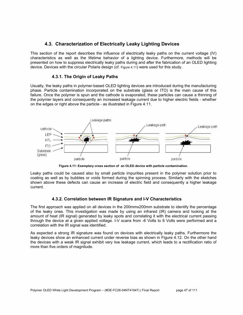
Polymer OLED White Light Development Program – (#DE-FC26-04NT41947) | Final Report page 47 of 111
4.3. Characterization of Electrically Leaky Lighting Devices
This section of the report describes the influence of electrically leaky paths on the current voltage (IV) characteristics as well as the lifetime behavior of a lighting device. Furthermore, methods will be presented on how to suppress electrically leaky paths during and after the fabrication of an OLED lighting device. Devices with the circular Polaris design (cf. Figure 4.11) were used for this study.
4.3.1. The Origin of Leaky Paths
Usually, the leaky paths in polymer-based OLED lighting devices are introduced during the manufacturing phase. Particle contamination incorporated on the substrate (glass or ITO) is the main cause of this failure. Once the polymer is spun and the cathode is evaporated, these particles can cause a thinning of the polymer layers and consequently an increased leakage current due to higher electric fields - whether on the edges or right above the particle - as illustrated in Figure 4.11.
Figure 4.11: Exemplary cross section of an OLED device with particle contamination.
Leaky paths could be caused also by small particle impurities present in the polymer solution prior to coating as well as by bubbles or voids formed during the spinning process. Similarly with the sketches shown above these defects can cause an increase of electric field and consequently a higher leakage current.
4.3.2. Correlation between IR Signature and I-V Characteristics
The first approach was applied on all devices in the 200mmx200mm substrate to identify the percentage of the leaky ones. This investigation was made by using an infrared (IR) camera and looking at the amount of heat (IR signal) generated by leaky spots and correlating it with the electrical current passing through the device at a given applied voltage. I-V scans from -6 Volts to 6 Volts were performed and a correlation with the IR signal was identified.
As expected a strong IR signature was found on devices with electrically leaky paths. Furthermore the leaky devices show an enhanced current under reverse bias as shown in Figure 4.12. On the other hand the devices with a weak IR signal exhibit very low leakage current, which leads to a rectification ratio of more than five orders of magnitude.

Polymer OLED White Light Development Program – (#DE-FC26-04NT41947) | Final Report page 48 of 111
Figure 4.12: I-V curve comparison for two OLED lighting devices with and w/o leaky paths.
A very good correlation between the IR signal and the reverse bias current was found as shown in Figure 4.13. This is expected as high leakage current will generate higher thermal energy through the leaky path “resistor”.
Figure 4.13: Correlation between IR intensity and leakage current.
4.3.3. Luminance Lifetime Behavior on OLED Lighting Devices with Electrically Leaky Paths
The effects of the leakage current on the luminance lifetime were also investigated. The lifetime experiment was set up at constant current conditions with the same initial luminance of 800cd/m2 for all devices. To monitor the behavior of the leakage paths over lifetime, IR measurements and leakage current measurements at a reverse bias of -5 Volts were performed before and after the lifetime run. Interestingly (as shown in Figure 4.14) no device shorted electrically during the duration of the constant current stress testing. A sample of 25 devices was used for this study. The difference in the decay rate between different devices is due to the different constant currents used to establish the same initial luminance (800 cd/m2).

Polymer OLED White Light Development Program – (#DE-FC26-04NT41947) | Final Report page 49 of 111
Figure 4.14: Lifetime progression of white polymer OLED lighting device with and w/o leaky paths.
However, after comparing the leakage current before and after the lifetime at 70 hours, a clear trend was observed. All devices with a leakage current less than 10-2 mA/cm2 showed no increase in the leakage current. However devices with a leakage current larger than 10-2 mA/cm2 showed a tenfold enhancement in the leakage current. Such devices will eventually develop an electrical short and a premature, most probably catastrophic, failure will occur.
4.3.4. Methods to Avoid Leaky Paths During Manufacturing
We designed an experiment to explore the effects of the polymer layer thickness on the magnitude of the leakage current. Two substrates with similar particle contaminations were manufactured with a normal PEDOT thickness (120nm) or an increased PEDOT thickness (400nm). Due to process limitations, however, the 400nm PEDOT layer was applied through two subsequent 200nm layers with in-between annealing step. After the device manufacturing, a complete characterization was made to show the influence of the increased layer thickness.
The IR analysis (as shown in Figure 4.15) demonstrated conclusively that on the plate made with thin PEDOT almost 50% of the devices showed one or more hot spots caused by electrically leakage paths, whereas the plate with the thick PEDOT showed no evidence of leaky paths in almost all devices.
Figure 4.15: IR signature (bright spots) comparison of OLED lighting panel plates with different process conditions.

Polymer OLED White Light Development Program – (#DE-FC26-04NT41947) | Final Report page 50 of 111
Finally devices with thicker PEDOT showed luminance non-uniformities attributed to thickness non-uniformities and an increase in operating voltage by a factor of two. These two issues can easily be addressed by optimizing the coating process to establish more uniform films and also using a more conducting PEDOT layer to minimize the voltage drop across this polymer layer.
4.3.5. Burn-in Methods to Suppress Electrically Leaky Paths
A “burn-in” step with a high reverse bias voltage is expected to reduce the amount of electrically leaky spots. According to this, the devices with leakage paths were put under a reverse bias condition of -30 Volts for 5 minutes. For the observation of the effects, an IR analysis before and after the burn-in was performed. Additionally, the leakage current was measured at a reverse bias of -5 Volts. To make sure that this burn-in does not affect the luminance lifetime the preconditioned devices were compared with unconditioned devices in a lifetime experiment.
After the pre-conditioning with -30 Volts, a clear difference in the IR signature as well as in the leakage current was observed. On 80% of the leaky devices the “hot” IR signatures were removed and in addition, the leakage current was also reduced. Spikes in the monitored current during the burn-in processing step, leads us to assume that the high electric field causes an increase in the current through the leaky path in a way that the generated heat “burns-out” the leakage paths.
This burn-in step, however, could cause optical defects (small specks) on the active area of the lighting device. Some of which are visible only in the illuminated state and others can be seen in the “off” state (possibly related to a burned-out cathode). However these small defects could be tolerable for lighting applications due to several reasons:
• Lighting devices are usually viewed from a distance, where these defects may not be noticeable. • Lighting devices are usually lighted up at pretty high luminance and the human eye usually avoids
looking straight into the source. • Diffuser films in front of the panel will also obscure these small defects.

Polymer OLED White Light Development Program – (#DE-FC26-04NT41947) | Final Report page 51 of 111
5. TASK 3: COLOR TUNABLE TILE DESIGN, FABRICATION, AND TEST 5.1. Introduction and Summary of Results
The major goal of the task was to make tiles where the color of the light emission could be tuned. This can be achieved by using three different light emitting polymers that emit in red, green and blue respectively. The electrical design had to be such that the relative intensities of the three colors could be individually controlled to tune the color of emission from the tile. As the design requires the use of three different polymers to be patterned on the same substrate, spin coating of the samples can not be used. Ink-jet printing was identified as the process of choice to make these tiles. The major milestones achieved in this task were as follows:
1. Design the substrate to achieve the goals of the task
2. Design a test setup to test the samples
3. Develop inks for each color polymer exhibiting good jet performance, result in flat films and good device performance
4. Develop a process to reliably print these inks on the substrate
5. Scale up the process to 200mm plates, including installation of new inkjet printing tool and plasma treatment tool
6. Optimize process and device structure to maximize device performance
When we started the process in early 2004, we were using 1”x1” samples. By the end of the project in October 2005, we had successfully developed a process to print color tunable samples on 200mm x 200mm plates. This involved identifying, buying and installing new equipment and developing the process to make the samples. One of the biggest challenges faced during the task was developing an ink formulation and printing process combination that allowed the printing of red, green and blue light emitting polymers into large 200mm x 200mm samples with less than 10 defects per plate. Achieving low leakage currents was also a major issue. This issue was resolved by developing a new ink for the hole-transporting layer and reducing the defect density from printing. High rectification ratios were demonstrated with the green and red polymers. Due to lack of time, the improved process to reduce the leakage current could not be applied to the blue polymer. We have made inkjet printed devices with performance close to that of comparable spin coated devices. The device performance achieved with inkjet printed samples is summarized in the table below; for comparison, the efficiencies of spin coated devices are also summarized in Table 5.1.
Color Efficiency IJ Samples (Cd/A)
Luminance (Cd/m2)
Volts (V)
Rectification Ratio (6V)
Efficiency of spin coated samples (Cd/A)
Red 1.25 130 4 >10,000 1.5-1.8
Green 9.16 1200 7 >10,000 10-12
Blue 1.85 260 7 N/A 3
Table 5.1: Characteristics of inkjet-printed tiles.
We have put together a demonstrator that comprises of two tiles, each 2”x3”, assembled with the drivers designed to control the intensity and color of light emission from these light sources. The pictures below show an image of such a demonstrator. The color tunability can be seen in Figure 5.1 below.
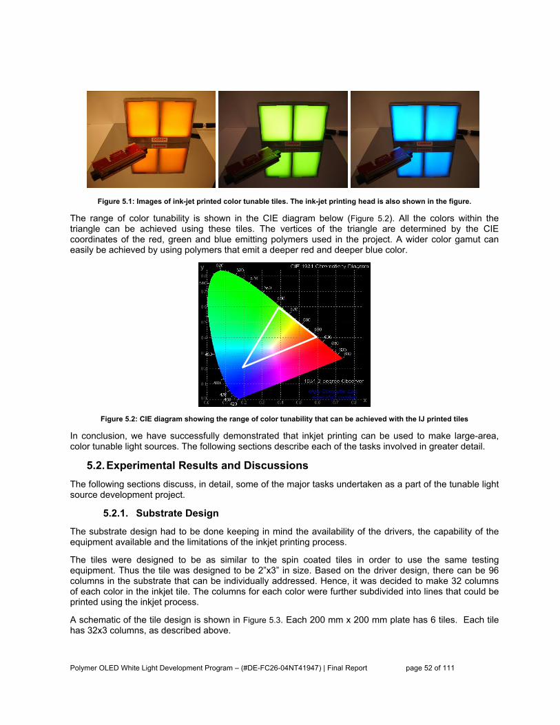
Polymer OLED White Light Development Program – (#DE-FC26-04NT41947) | Final Report page 52 of 111
Figure 5.1: Images of ink-jet printed color tunable tiles. The ink-jet printing head is also shown in the figure.
The range of color tunability is shown in the CIE diagram below (Figure 5.2). All the colors within the triangle can be achieved using these tiles. The vertices of the triangle are determined by the CIE coordinates of the red, green and blue emitting polymers used in the project. A wider color gamut can easily be achieved by using polymers that emit a deeper red and deeper blue color.
Figure 5.2: CIE diagram showing the range of color tunability that can be achieved with the IJ printed tiles
In conclusion, we have successfully demonstrated that inkjet printing can be used to make large-area, color tunable light sources. The following sections describe each of the tasks involved in greater detail.
5.2. Experimental Results and Discussions The following sections discuss, in detail, some of the major tasks undertaken as a part of the tunable light source development project.
5.2.1. Substrate Design
The substrate design had to be done keeping in mind the availability of the drivers, the capability of the equipment available and the limitations of the inkjet printing process.
The tiles were designed to be as similar to the spin coated tiles in order to use the same testing equipment. Thus the tile was designed to be 2”x3” in size. Based on the driver design, there can be 96 columns in the substrate that can be individually addressed. Hence, it was decided to make 32 columns of each color in the inkjet tile. The columns for each color were further subdivided into lines that could be printed using the inkjet process.
A schematic of the tile design is shown in Figure 5.3. Each 200 mm x 200 mm plate has 6 tiles. Each tile has 32x3 columns, as described above.

Polymer OLED White Light Development Program – (#DE-FC26-04NT41947) | Final Report page 53 of 111
Figure 5.3: 200 mm x200 mm plate with 6 tiles (left), and single tile showing the 96 columns and anode and cathode contacts (right).
5.2.2. Equipment Requirements to Achieve the Goals
In order to make the RGB tiles using inkjet, it was necessary to buy some new equipment. Before the inkjet plates can be printed, the plates have to undergo a surface treatment. The uniformity requirements for such large tiles meant, a bigger plasma treatment tool was needed to perform the surface treatment of the tiles before inkjet printing. In order to do this, several plasma tools were identified and preliminary testing carried out with the vendors. Based on the initial tests, the Tepla 4011 tool (Figure 5.4) was identified to be the most suitable tool for the process. The tool was ordered and to be delivered in October 2004. However, the tool was delivered in early January 2005.
In addition to the plasma tool, a new printer was needed to handle the large sized substrates (200mmx200mm) to be printed for the DOE project. The Litrex 140P tool (Figure 5.4) was ordered in March 2004. The acceptance testing of the tool, at the vendor site, was carried out in August/September 2004 and the tool installation, in September 2004, was followed by a final acceptance test. Industrial inkjet tools for the precision printing are still an active area of development; this is evident in the performance of the tool which leaves much to be desired. As there are no alternatives at present in the market, it was decided to use this tool and work with the manufacturer to further improve the tool for lighting and display applications.
As will be discussed later, the long lead time for delivery of the plasma tool and issues with the Litrex 140P printer greatly limited what we could achieve in the first year of the project.

Polymer OLED White Light Development Program – (#DE-FC26-04NT41947) | Final Report page 54 of 111
Figure 5.4: Tepla 4011 Plasma tool (left), and Litrex 140P industrial inkjet printer (right).
As the process is scaled up to 200 mm plates, we also need to use more uniform hot plates than the ones we had been using at the time; the cathode deposition and encapsulation process needed to be optimized as well. We decided to use the existing infrastructure in the pilot line for these tasks.
5.2.3. Test set and Driver Design and Development
A new test jig to test the tiles was developed and delivered in the first week of October 2004. In addition, drivers for the RGB tiles have been developed. These two tasks are described in more detail in the next section of this report.
5.2.4. Ink Development
One of the major goals of this task was to develop inks for PEDOT and the red, green and blue polymers that would result in:
1. Good jetting performance
2. Inks that are stable with time (shelf life)
3. Flat uniform films
4. High efficiency and long lifetimes for devices
In this section we describe the process and results of developing a PEDOT and LEP inks.
5.2.4.1. PEDOT Inks A strong effort was put into this process to develop the PEDOT and LEP inks as this is the basis of all inkjet printing. In order to achieve stable printing the inks must have a stable jetting behavior. To be compatible with the multi-nozzle Spectra printheads, the inks must have certain physical properties like viscosity in the range of 8-14 cPs and a low surface tension to get good wetting of the ink on the substrate. The PEDOT ink was formulated to meet the above specifications and its jetting properties were tested with the spectra SX-128 printhead. The films achieved with the new PEDOT formulations are flat and uniform (>90% of the area of the film has a thickness variation of less than 5%).

Polymer OLED White Light Development Program – (#DE-FC26-04NT41947) | Final Report page 55 of 111
-5000
5000
15000
25000
35000
45000
55000
0 50 100 150 200 250 300
Distance (um)
Heig
ht (A
)
Figure 5.5: Optical micrograph of a printed PEDOT sample. The films are uniform and repeatable. The graph on the right shows a Dektak profile of the film which confirms that the films are flat.
Peak to Valley Roughness <±10 nm
Uniformity of thickness 94% at ± 5% of
Latency time for Jetting >1 hr
Dwell time for Jetting >2 hours
Viscosity of ink 14 cP
Surface Tension of ink 47 dynes/cm
Conductivity of printed PEDOT film 10 Ω/cm
Shelf Life of ink >30 days
Table 5.2: Summary of Jetability and film formation of PEDOT.
Table 5.2 summarizes the jetting and film formation of the PEDOT ink. The ink performs extremely well and meets all the requirements for making lighting tiles. Latency time and Dwell time are parameters that are extremely important for the stability and reliability of inkjet process. The longer the latency and dwell times, the better is the reliability of printing. In the case of PEDOT the inks are very reliable and reproducible.
4.3.5.1. LEP Inks
Inks were also developed for each of the red, green and blue polymers. The LEP inks are made using organic solvents which have high evaporation rates and these result in the relatively low latency and dwell times for these inks. In comparison, PEDOT ink is water based and is much more stable due to the lower evaporation rate of water compared to organic solvents.

Polymer OLED White Light Development Program – (#DE-FC26-04NT41947) | Final Report page 56 of 111
Achieving flat and uniform LEP inks is considerably more difficult and a lot of work had to be done to develop these inks. The inks that we have developed now result in films that are much more uniform than we could achieve at the beginning of this project. This has been achieved by using combinations of multiple solvents that result in the good jetting of the inks by controlling its interactions with the print-head as well as optimal drying properties that result in flat and uniform films on the substrate. Figure 5.6 shows the photoluminescence image of the films before and after optimization. It is evident from the pictures that the films obtained now are much more uniform.
Figure 5.6: PL image of printed inks. Inks were optimized for spin coating (left), and PL image of printed inks. Inks were optimized for inkjet printing (right).
The importance of achieving flat films can be seen clearly when the devices are electrically operated to emit light. Figure 5.7 shows the Electroluminescence images of devices made with different green inks. The picture on the left is from devices made with inks optimized for spin coating while the picture on the right has been printed with inks optimized for inkjet printing. With the inks that are optimized for spin coating only a small part of each pixel is emitting light. This would require that the device be run at higher current densities to achieve the same level of brightness as a device where a large fraction of the pixel is emitting light. The higher “fill-factor” of the pixel can be achieved with the optimized inks as seen in Figure 5.7. This will allow the device to be operated at lower voltages resulting in both higher efficiencies as well as leading to longer lifetimes as the devices are now operating at lower current densities.
Figure 5.7: Electroluminescence image of device made with inks optimized for spin-coating (left), and Electroluminescence image of device made with inks optimized for IJ printing (right)

Polymer OLED White Light Development Program – (#DE-FC26-04NT41947) | Final Report page 57 of 111
4.3.5.1. Jetting Stability of Inks
The inks have been developed keeping in mind the production requirements. Thus the inks have to be printable at high frequencies. The jettability studies show that the PEDOT ink can be used up to 7 kHz while the LEP inks have been shown to be usable up to ~4 kHz. It is clear from Figure 5.8 that the PEDOT ink developed can be used to jet at high frequencies up to at least 7000 Hz which is the limit of the electronics in the printer. In order to achieve the high frequencies, we had to modify the Litrex 80L printer and add a pressure control system to control the pressure in the printhead during jetting. Adding the pressure control increases the frequencies at which we can print PEDOT by at least a factor of 2. In addition, the new tool, the Litrex 140P, was ordered with a similar pressure control system that was developed by the vendor. In order to obtain stable jetting several parameters had to be optimized, including the drive waveforms used to create the drops in the printhead and the pressure used for jetting. Figure 5.8 shows the effect of various parameters on the jetting properties of the ink. The drive waveform must be optimized to get the most energy efficient drop generation.
Velocity at different frequencies with different back pressure
0
1
2
3
4
5
6
7
8
9
0 2000 4000 6000 8000frequency in Hz
velo
city
in m
/s
-0.35 psi -0.40 psi-0.45 psi
Velocity at different pulsewidthes with different voltages
0
2
4
6
8
10
12
4.5 5.5 6.5 7.5 8.5
pulsewidth in us
velo
city
in m
/s60V/65V80V/85V100V/105V
Figure 5.8: Jetting stability of the PEDOT ink. PEDOT can be printed at high frequencies up to at least 7000 Hz (left), and Effect of the drive parameters for PEDOT. The pulse width should be chosen to achieve maximum velocity (right).
4.3.5.1. Shelf Life of Inks
The inks also had to meet shelf life requirements. The shelf life has been tested at various temperatures to study the accelerated degradation of the inks. Initially we faced several problems with the shelf life of the inks. These issues were resolved with a change in the process of making the inks and with the new process the inks have been found to be stable for several weeks. Fig. 7 shows the stability of viscosity of the ink over time at different temperatures.
-5.0
0.0
5.0
10.0
0 5 10 15 20 25 30 35 40 45 50
Days
Visc
., %
cha
nge
% 70 C% 50C% room% 8C
Figure 5.9: Shelf life studies of red ink. The viscosity of the ink is stable for several weeks.

Polymer OLED White Light Development Program – (#DE-FC26-04NT41947) | Final Report page 58 of 111
5.2.5. Inkjet Process Development
4.3.5.1. Plasma Process
The plasma process is used to control the surface properties of the substrate. The surface properties play a major role in controlling the spreading of drops and the confinement of the ink in the desired locations. In addition the plasma process is necessary to have a flat and uniform film that is necessary to achieve the high fill factors as explained in the previous section. Thus it is very important to have a uniform and reproducible plasma process. The data in Figure 5.10 shows the results of this optimization; a process was developed that was stable and had a large process window, thus resulting in a repeatable process. A thorough characterization of our plasma system shows that there is a very small 3”x3” area where the plasma process is uniform. Thus, although the process is repeatable, the process can only be used for single tiles, 2”x3” in size, due to the limitations of the uniformity of the plasma chamber.
In order to process larger plates we have carried out tests and identified a new plasma tool (Tepla 4011). A process was developed with the vendor that would result in the desired surface modifications and result in a process that is uniform across large substrates, much greater in size than the 200 mm x 200 mm. Figure 5.10 shows the map of the uniformity of the new tool. As the tool met our needs and specifications, the tool was ordered and was expected to be delivered in September, but the delivery was delayed significantly. The tool was delivered in early January 2005. In order to process one tile at a time we had to develop a makeshift encapsulation setup as well. The plasma process using the current tool was optimized to achieve the required surface properties reproducibly. It is evident that the new tool would have a large effect on the uniformity of the process and is expected to enable the printing of 200mmx200mm plates in one shot. Thus all the samples processed in Year 1 of the project were made with single tiles, while larger samples were made in the second year of the project beginning in January 2005.
50.0
60.0
70.0
80.0
90.0
100.0
110.0
0 200 400 600 800 1000Plasma treatment duration in seconds
Con
tact
ang
le o
f Bay
tron
on re
sist
new processOld process
Figure 5.10: Developing a stable process window for the plasma process in San Jose (left) and Uniformity of surface properties of across a 350mm x350 mm substrate using the new Tepla plasma chamber (right).
4.3.5.1. PEDOT Printing:
The plasma, ink and processing conditions had to be optimized to achieve flat and uniform films of PEDOT on the substrate. The process involved optimizing the number of drops per unit length as well as the placement positions of the drops to make sure we have completely filled lines as well as the right thickness for the film. Figure 5.11 (left) shows some pictures with the different drops per pocket as well as the different positions of the drop placement. If there are too few drops per pocket, the lines are not completely filled. The films achieved with the optimized PEDOT formulations and processes are flat and uniform as shown in Figure 5.11 (right).
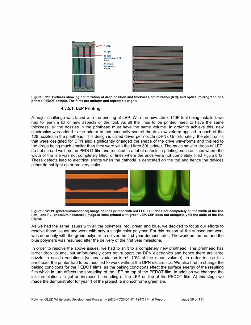
Polymer OLED White Light Development Program – (#DE-FC26-04NT41947) | Final Report page 59 of 111
1 dpp
34 dpp
45 dppnecessary to fill linesAverage thickness: 90nm
Figure 5.11: Pictures showing optimization of drop position and thickness optimization (left), and optical micrograph of a printed PEDOT sample. The films are uniform and repeatable (right).
4.3.5.1. LEP Printing
A major challenge was faced with the printing of LEP. With the new Litrex 140P tool being installed, we had to learn a lot of new aspects of the tool. As all the lines to be printed need to have the same thickness, all the nozzles in the printhead must have the same volume. In order to achieve this, new electronics was added to the printer to independently control the drive waveform applied to each of the 128 nozzles in the printhead. This design is called driver per nozzle (DPN). Unfortunately, the electronics that were designed for DPN also significantly changed the shape of the drive waveforms and this led to the drops being much smaller than they were with the Litrex 80L printer. The much smaller drops of LEP, do not spread well on the PEDOT film and resulted in a lot of defects in printing, such as lines where the width of the line was not completely filled, or lines where the ends were not completely filled Figure 5.12. These defects lead to electrical shorts when the cathode is deposited on the top and hence the devices either do not light up or are very leaky.
Figure 5.12: PL (photoluminescence) image of lines printed with red LEP. LEP does not completely fill the width of the line (left), and PL (photoluminescence) image of lines printed with green LEP. LEP does not completely fill the ends of the line (right).
As we had the same issues with all the polymers, red, green and blue, we decided to focus our efforts to resolve these issues and work with only a single color polymer. For this reason all the subsequent work was done only with the green polymer to deliver the first year demonstrator. The work on the red and the blue polymers was resumed after the delivery of the first year milestone.
In order to resolve the above issues, we had to shift to a completely new printhead. This printhead has larger drop volume, but unfortunately does not support the DPN electronics and hence there are large nozzle to nozzle variations (volume variation is +/- 10% of the mean volume). In order to use this printhead, the printer had to be modified to work without the DPN electronics. We also had to change the baking conditions for the PEDOT films, as the baking conditions effect the surface energy of the resulting film which in turn effects the spreading of the LEP on top of the PEDOT film. In addition we changed the ink formulations to get an increased spreading of the LEP on top of the PEDOT film. At this stage we made the demonstrator for year 1 of the project, a monochrome green tile.

Polymer OLED White Light Development Program – (#DE-FC26-04NT41947) | Final Report page 60 of 111
5.2.6. Year 1 Deliverable: Green Monochrome Tile
With the new head, inks and new process we managed to make some working samples in December 2004. Figure 5.13 shows pictures of these tiles under operation. It is evident that there are several defects in the tile. There are some missing lines that are caused by printing defects. There are line to line non-uniformities due to the difference in thickness of the lines printed using different nozzles. In addition we have seen some issues with shorting of the lines due to the wicking of the polymer next to the mushroom resist. The strong capillary forces next to the mushroom layer make it essential for us to have a very good control of the drop placement accuracy which we do not have with the printheads used to make these devices. It is also evident that we can individually address each of the lines, which confirms that the tile design and the electronics are functioning as designed.
Figure 5.13: Electroluminescence picture of a tile printed with the green polymer. Some defects are clearly visible (left); and green tile with every third line addressed (right).
The I-V characteristic of the green tile was measured and is shown in Figure 5.14. The maximum efficiency achieved is 5.75 lm/W (7.6 Cd/A) at 300 Cd/m2 luminance and the efficiency is 4.2 lm/W (7.4 Cd/A) at ~1200 Cd/m2.
0.000
0.004
0.008
0.012
0.016
0.020
0 2 4 6 8
Voltage (V)
Cur
rent
(A)
0
200
400
600
800
1000
1200
1400
1600
Lum
inan
ce (C
d/m
2)
CurrentLuminance
0.0
1.02.0
3.0
4.05.0
6.0
7.08.0
9.0
0.0 2.0 4.0 6.0 8.0
Voltage (V)
Effi
cien
cy (C
d/A
)
Efficiancy(Cd/A)Power Efficiency (Lm/W)
Figure 5.14: Current, Voltage, Luminance curve (left), and Efficiency vs. Voltage curves for a green tile

Polymer OLED White Light Development Program – (#DE-FC26-04NT41947) | Final Report page 61 of 111
5.2.7. End of Year 1 status and Goals for Year 2
We demonstrated, with the year 1 demo tile, that inkjet printing can be used to make tiles for lighting; however, there were several issues that needed to be resolved at that point. These issues drove the work that we performed starting January 2005. We focused on developing a stable and reproducible process on 200mm plates to produce RGB tiles and work on improving the efficiency of the device. As a milestone we set up a target of making RGB demonstrators by July 2005.
5.2.8. Scaling Up to 200 mm Plates
Our main goal for this year was to move away from processing single tiles and scale up the process to larger plates. The logical next step was to scale up the process to 200mm plates as the pilot line in San Jose is equipped to run 200 mm plates. This would allow processes such as cathode deposition and encapsulation to be carried out by the technicians and engineers focusing on these processes and free up the inkjet team to focus on developing the plasma and inkjet processes.
The major tasks the inkjet group focused on are listed below:
1. Optimization of plasma process
2. PEDOT printing process development
3. Printing process, including ink development, for each of the red, green and blue LEP’s
4. Making the RGB demonstrator
Each one of these tasks is described in detail below.
4.3.5.1. Plasma Process
In order to achieve this goal OSRAM purchased a Litrex 140P printer in August 2004. This printer is capable of handling large plates, up to 270mm x370 mm. However, we could not process 200 mm plates till the plasma treatment tool from Tepla was delivered and installed in the clean room in January of 2005.
After initial testing confirmed that the plasma tool was performing according to specifications we focused on developing the process. The plasma treatment is used to increase the surface energy of ITO, while reducing the surface energy of the photo-resist in order to confine the inks in the active regions of the device. The major process requirements are described in Table 5.3.
ITO Photo-resist
Contact Angle target with PEDOT (time = 0) 17° 93°
Uniformity of contact angle ±1.5° ±1.0°
Contact angle after 30 minutes <20° 93 ± 2°
Table 5.3: Requirements of the surface properties after plasma process.

Polymer OLED White Light Development Program – (#DE-FC26-04NT41947) | Final Report page 62 of 111
In the initial set of experiments, Design of Experiments (DoE) was used to identify the major factors that influence the surface energies of the two surfaces after plasma treatment. The factors that were varied were: pressure, process time, gases used, gas flow rates, and power. As shown in Figure 5.15 below, the major factor by far was the pressure at which the process is carried out. Other important factors were the flow rates of the different gases used. These factors were then optimized to achieve the targeted contact angle as well as the stability of the surface energies.
The uniformity of the contact angle is measured across a 400mm x 400 mm area as shown in Figure 5.16 below. Four 200 mm plates were used to carry out this test and the positions used for measurements are depicted in Figure 5.16 below. The results of the uniformity are also shown in the Figure 5.16. The data shows that the contact angle on ITO is quite uniform over a large area. Based on these results, we selected a 200mm x 200 mm area that would result in the best uniformity for future work.
Pressure Time Power Gas1 Gas2
Pressure Time Power Gas1 Gas2 Figure 5.15: Relative impact of various factors on the contact angles of PEDOT on ITO (left), and photo-resist (right).
151617181920
1 2 3 4 5 6 7 8arbitrary positions of plate
ITO
con
tact
ang
le
with
Ped
ot
Figure 5.16: Schematic showing locations of contact angle measurements (left), and the actual contact angle data (right).
After completing the plasma treatment, the next step in the process is PEDOT printing. The surface profile and uniformity of the resulting PEDOT film are strongly dependent on the surface energies of ITO and photo-resist. Thus, in addition to meeting the target contact angle and uniformity at time zero, the surface energies also need to be stable during the time the PEDOT is being printed to ensure that the PEDOT printed in the first pixels to be printed on the plate is the same as the PEDOT that is printed in the last pixels. As it takes us about 15 minutes to print the PEDOT, the surface energy needs to be stable for 30 minutes to allow for any process variations.
While it is relatively easy to stabilize the surface energy of the photo-resist, it is quite challenging to find process conditions that result in a stable surface energy of ITO. We increase the surface energy of ITO in order to improve the spreading of PEDOT on ITO; this makes the ITO surface highly reactive and inherently unstable. However, we have identified process conditions that result in an ITO surface stable enough to meet our process needs. Figure 5.17 shows the change in contact angle of PEDOT on ITO with time.

Polymer OLED White Light Development Program – (#DE-FC26-04NT41947) | Final Report page 63 of 111
151617181920
0 5 10 15 20 25Time (min)
ITO
Con
tact
Ang
le
with
Ped
ot
Figure 5.17: Figure showing the stability of the surface energy of ITO with time.
4.3.5.1. PEDOT Printing
After the plasma process was developed we confirmed that the PEDOT printing process met our requirements. A process was developed to print uniform films with the required thickness of PEDOT on 200 mm plates. The PEDOT process scaled up to the 200 mm plates without any major issues.
5.2.9. Optimization of RGB Printing
To optimize RGB printing we decided to work on monochrome tiles to optimize the printing for each of the three LEP’s. Based on experience in December, we knew that our biggest challenge would be to find a process to completely fill all the pixels. As we had a lot of issues filling lines, we decided to print into pockets.
4.3.5.1. Drying Stains
As we started printing in 200 mm plates, we noticed drying patterns on the cells. This resulted in non-uniform emission from the samples. Figure 5.18 illustrates the non-uniformity within a display as well as shows another display from the same plate that is fairly uniform. A pattern is clearly visible in the picture on the right, while the picture in the left is an extreme case where a major portion of the device does not light up.
Figure 5.18: Non-uniformity in electroluminescence due to drying stains.

Polymer OLED White Light Development Program – (#DE-FC26-04NT41947) | Final Report page 64 of 111
Figure 5.19 below shows the non-uniformity of luminance within a 5x6 array of devices on a 200mm plate that resulted from the drying effects.
Figure 5.19: Distribution of emission intensity in samples across a plate.
The “drying stains” are a result of non-uniform drying of the LEP layers. In order to resolve this issue, we had to change the printing conditions as well as the drying conditions for LEP printing in order to control the drying of the LEP. With these changes, we could obtain a uniform drying across the whole 200 mm plate.
4.3.5.1. Pixel Filling
As mentioned earlier, we expected that it would be difficult to fill all the pixels in a sample and this indeed was a major challenge we had to resolve. Each of the 2”x3” lighting tile has >150,000 pockets and we had to develop a process such that none of the pockets was incompletely filled.
By changing the baking conditions of PEDOT we were able to completely fill the pockets with the LEP. This is illustrated in Figure 5.20 below which shows two samples printed in the same way, except for the different baking conditions used for PEDOT.
Figure 5.20: Photoluminescence images showing pockets with mouse-bites (left), and pockets without mouse-bites (right) printed with the new optimized process.
After optimizing the process for the green polymer, we repeated the process with the red and the blue polymers as well. To our surprise with inks made using the same solvents as the green polymer, we could not completely fill the pockets with the red and the blue polymers. We had to develop new inks for both of these polymers in order to completely fill the pockets.
1 2 3 4 5 61
2
3
4
5
Rown Number
Col
umn
Num
ber 120-140
100-12080-10060-8040-6020-400-20

Polymer OLED White Light Development Program – (#DE-FC26-04NT41947) | Final Report page 65 of 111
In order to better understand the root cause of the drying effects we decided to make videos of the drying of these layers. This process led us to realize that the incomplete filling of the pixel was not a filling issue, but rather an effect of mass transport during the process of drying of the liquid to form a film. This is illustrated in the pictures in Figure 5.21 below. The picture on the left shows an image of the pixel right after the drops are deposited in the pocket. It is evident that the pocket is completely filled with the liquid. However, as the liquid dries to form a film, it also starts to recede from one of the edges (the bottom edge in this case) and finally when the film is dry, there is a gap between the edge of the pocket and the edge of the dried film.
Figure 5.21: Pictures of a pocket after the deposition of the liquid (left), and after the liquid dries into a solid film (right).
With our recent efforts to understand this issue we have concluded that the incomplete filling of the pixels is a complex process that is a combination of surface tension gradients (Marangoni effect) that develop at the edges of drying patterns and other forces that develop when mixtures of two or more solvents are drying. Unfortunately we were not able to address this issue completely to gain a full understanding of the issue. However, we did develop inks for both blue and red polymers where we could significantly reduce these effects however we could not completely eliminate them.
4.3.5.1. Baking of LEP
As mentioned earlier, on scaling up to a 200mm sample, we needed to use new hot plates that were large enough to handle the samples. When the first few plates were made, we noticed some bright and dark spots on the device. An image illustrating this is depicted below (Figure 5.22). The origin of these spots was traced to the vacuum holes and the lift pins on the hot plate used to bake the LEP. We had to develop a new process and modify the position of the lift pins in order to eliminate these patterns on the sample.
Figure 5.22: Picture showing bright spots due to the vacuum holes in the hot plate.

Polymer OLED White Light Development Program – (#DE-FC26-04NT41947) | Final Report page 66 of 111
4.3.5.1. Improving Fill Factor
Another challenge that we faced was to improve the fill factor of the tiles. The fill factor is defined as the percent of available area that is emitting light. Initially we had a very poor fill factor due to the non-uniformity of the LEP layer. Although we had developed inks and process to improve the fill factor for making the single 2”x3” tiles used to make the demonstrators in the first year, the issue resurfaced when we scaled up to 200 mm plates with the same inks and process. As seen in the pictures below (Figure 5.23) initially only the edges of the pockets were emitting light, since then we have managed to improve the fill factor significantly. This was done through a combination of process and ink changes.
Figure 5.23: EL picture showing poor fill factor (left), and EL picture with improved fill factor (right).
5.2.10. Choosing the Best Ink
In the ink development part of the project we ended up developing several inks that met jetting and pixel filling requirements mentioned above. However the final decision on the best ink could only be made after we made working devices using all these inks and evaluated the device performance. We decided to make devices with different inks and for each ink with different thicknesses of the LEP layer to optimize the operating voltage and efficiency. The results of these tests are summarized in Figure 5.24 below. Each bar in the figure represents the average performance of devices on one plate; each of the plates has six 2”x3” tiles. Based on this data we picked the best ink and LEP thickness for printing each color.
Figure 5.24: Summary of the performance of devices made with different inks.
0
0.2
0.4
0.6
0.8
1
1.2
Forw
ard
Curr
ent (
A)
00.1
0.20.30.40.5
0.60.7
Reve
rse
Cur
rent
(A)
0
2
4
6
8
10
12
Rec
Ratio
0.11
10100
100010000
5699 5701 5735 5736 5737 5738 5739 5898 5900 5903 5904 5901 5902 5909 5910 5911 5913 5914 5915 5916 5917 5918 5919
IJL02 IJL03 IJL04 IJL05 IJL06 IJL07 IJL08 IJL09
Lum
inan
ce (5
V)
COLOR OF BAR ==> COLOR OF LEP
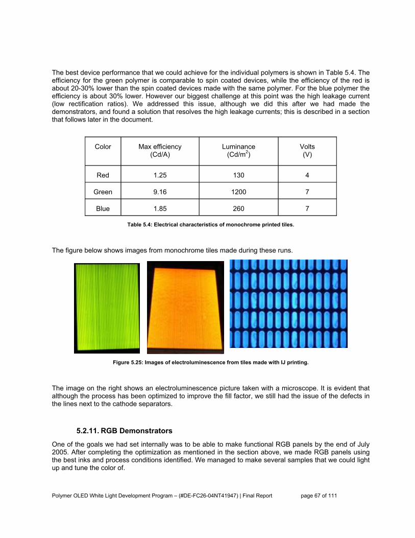
Polymer OLED White Light Development Program – (#DE-FC26-04NT41947) | Final Report page 67 of 111
The best device performance that we could achieve for the individual polymers is shown in Table 5.4. The efficiency for the green polymer is comparable to spin coated devices, while the efficiency of the red is about 20-30% lower than the spin coated devices made with the same polymer. For the blue polymer the efficiency is about 30% lower. However our biggest challenge at this point was the high leakage current (low rectification ratios). We addressed this issue, although we did this after we had made the demonstrators, and found a solution that resolves the high leakage currents; this is described in a section that follows later in the document.
Color Max efficiency (Cd/A)
Luminance (Cd/m2)
Volts (V)
Red 1.25 130 4
Green 9.16 1200 7
Blue 1.85 260 7
Table 5.4: Electrical characteristics of monochrome printed tiles.
The figure below shows images from monochrome tiles made during these runs.
Figure 5.25: Images of electroluminescence from tiles made with IJ printing.
The image on the right shows an electroluminescence picture taken with a microscope. It is evident that although the process has been optimized to improve the fill factor, we still had the issue of the defects in the lines next to the cathode separators.
5.2.11. RGB Demonstrators
One of the goals we had set internally was to be able to make functional RGB panels by the end of July 2005. After completing the optimization as mentioned in the section above, we made RGB panels using the best inks and process conditions identified. We managed to make several samples that we could light up and tune the color of.

Polymer OLED White Light Development Program – (#DE-FC26-04NT41947) | Final Report page 68 of 111
Tiles were then put together in the form of a demonstrator by integrating them with the drivers that were developed by the product development group as part of a separate task under the DOE project. Each board is capable of driving two tiles at the same time. The details of the drivers are described in a different section in this report. We also identified the best diffusers to use with the inkjet printed lighting tiles to make sure that the tiles appeared uniform and that the individual lines for each color were not visible to the user while ensuring that there is a minimal loss in the intensity of out-coupled light. The demonstrator had an intensity of ~200 nits after the diffuser; the loss in intensity due to the diffuser is measured to be close to 5%. Figure 5.26 below shows the demonstrator that we put together and demonstrate the color tunability of the light source.
Figure 5.26: Images showing the demonstrators made with the tunable R,G,B light source.
Although the above images look quite nice and uniform, these were achieved by choosing the best available tiles that we had. We faced few issues when we made most of the RGB tiles:
1. There was a lateral non uniformity within the tiles (horizontal direction in the pictures above). As we go from the left of the tile to the center and then to the right, the intensity first falls and then rises again. The intensity is the lowest in the central vertical section of the tile.
2. The intensity falls as we go farther away from the contacts (vertical direction in picture above). This shows up as a decrease in intensity as we go from the bottom to the top of the tiles. This drop is clearly evident in the red emitter, but is not significant for the green and the blue polymers which result in fairly uniform emission.
3. In some of the samples, we notice bright lines. This is a manifestation of the fact that the columns with pockets next to the cathode separator are brighter than the rest of the columns.
The first non-uniformity is a result of the resistive drop in the anode, while the second non-uniformity is due to the high leakage currents. The third issue is a result of a tile design that is linked to processing tolerances. These issues are discussed in more details below.
4.3.5.1. Horizontal Intensity Drop: Resistive Drop in the Anode
As seen in the Figure 5.27 below, a gradient can be seen in the emission intensity with the highest intensity at the left and right edges of the lighting tile. The middle of the tile is darker. This is a result of the tile design. We are using a common anode design in the tile. In the left schematic below, the dark blue boxes are the ITO regions. The light blue regions represent the metallization for the contacts. The metal lines run along the left and right edges of the tile to reduce any voltage drops going from top to bottom. The anode is electrically connected to the power supply via two contacts at the left and right bottom edges as shown in the schematic below. The schematic on the right shows the cathode separator layers that are used to define individual lines for each of the three colors.

Polymer OLED White Light Development Program – (#DE-FC26-04NT41947) | Final Report page 69 of 111
Figure 5.27: Picture showing the gradients in emission intensity across a tile and the schematics of the tile.
The schematic below is a zoomed image of the bottom right corner of the tile and shows the individual cathode contacts (light blue) connecting to each of the 96 lines. On the right bottom corner we can see the anode contact.
The lines are addressed by using individual cathodes for each of the lines as shown in the schematic below. However, due to this design, there is a potential drop as we go from the right or left edge of the tile (next to the anode contact) to the middle of the tile. As the current has to flow from the anode to the middle of the tile and then out through the cathode, there is a larger voltage drop for lines in the middle than for the lines closer to the anode. This results in the lines near the edges of the tiles being brighter than the lines in the middle of the tile. Due to the large size of the active area, the current densities needed are high, and as a result the resistive voltage drop, V= I2*R, is fairly significant and results in a visible intensity variation.
Figure 5.28: Schematic showing the individual cathode lines and the anode contacts.
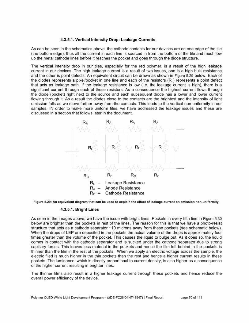
Polymer OLED White Light Development Program – (#DE-FC26-04NT41947) | Final Report page 70 of 111
4.3.5.1. Vertical Intensity Drop: Leakage Currents
As can be seen in the schematics above, the cathode contacts for our devices are on one edge of the tile (the bottom edge); thus all the current in each line is sourced in from the bottom of the tile and must flow up the metal cathode lines before it reaches the pocket and goes through the diode structure.
The vertical intensity drop in our tiles, especially for the red polymer, is a result of the high leakage current in our devices. The high leakage current is a result of two issues, one is a high bulk resistance and the other is point defects. An equivalent circuit can be drawn as shown in Figure 5.29 below. Each of the diodes represents a pixel/pocket in one line and each of the resistors (RL) represents a point defect that acts as leakage path. If the leakage resistance is low (i.e. the leakage current is high), there is a significant current through each of these resistors. As a consequence the highest current flows through the diode (pocket) right next to the source and each subsequent diode has a lower and lower current flowing through it. As a result the diodes close to the contacts are the brightest and the intensity of light emission falls as we move farther away from the contacts. This leads to the vertical non-uniformity in our samples. IN order to make more uniform tiles, we have addressed the leakage issues and these are discussed in a section that follows later in the document.
RL -- Leakage ResistanceRA -- Anode ResistanceRC -- Cathode Resistance
RL RL RL RL
RA RA RA RA
RC RC RC RC
Figure 5.29: An equivalent diagram that can be used to explain the effect of leakage current on emission non-uniformity.
4.3.5.1. Bright Lines
As seen in the images above, we have the issue with bright lines. Pockets in every fifth line in Figure 5.30 below are brighter than the pockets in rest of the lines. The reason for this is that we have a photo-resist structure that acts as a cathode separator ~10 microns away from these pockets (see schematic below). When the drops of LEP are deposited in the pockets the actual volume of the drops is approximately four times greater than the volume of the pocket. This causes the liquid to bulge out. As it does so, the liquid comes in contact with the cathode separator and is sucked under the cathode separator due to strong capillary forces. This leaves less material in the pockets and hence the film left behind in the pockets is thinner than the film in the rest of the pockets. When we apply an electric voltage across the sample, the electric filed is much higher in the thin pockets than the rest and hence a higher current results in these pockets. The luminance, which is directly proportional to current density, is also higher as a consequence of the higher current resulting in brighter lines.
The thinner films also result in a higher leakage current through these pockets and hence reduce the overall power efficiency of the device.

Polymer OLED White Light Development Program – (#DE-FC26-04NT41947) | Final Report page 71 of 111
Figure 5.30: EL pictures depicting the bright lines observed in the tiles (left), and a schematic of the tile layout showing the mushroom and the pockets (right).
This issue can be resolved by increasing the distance between the cathode separator and the pockets right next to it. We implemented this solution in a design with smaller tiles and have confirmed that we can eliminate this issue. However, we did not have the opportunity to implement this solution to the 2”x3” tiles before the project ended.
4.3.5.1. Color Gamut of RGB Tiles and Efficiency of White
One of the reasons we are pursuing RGB tiles is the ability to tune colors using such a lighting structure. The range of color tunability of the tiles is referred to as the “Color-Gamut” of the tile. The color gamut is determined by the color coordinates of the individual red, green and blue emitters and is represented by the triangle that joins the three points on a CIE diagram. The image below shows the color coordinates of the three polymers we are using and the range of color tunability with these polymers.
One of the things to notice on the CIE diagram (Figure 5.31) is the fact that the red polymer we use, is more orange than red. The reason for using this polymer was that this had the highest efficiency of all the available red polymers. Any color in the color triangle can be achieved by using the right intensities of the three different emission colors. An unfortunate consequence of the selection of this set of three polymers is that in order to achieve a white color, we need to use a less than 20% of green and about 40% each of red and blue. As a result, the efficiency of the white light source is rather poor as both the red and blue have low efficiencies and the higher efficiency of the green polymer can not be exploited to achieve higher efficiencies in the white. Based on the efficiencies we have achieved with the red, green and blue polymers, the highest efficiency we can achieve in white is 3 Cd/A, which falls far short of the specification for the project.
Figure 5.31: The range of color tunabililty of the tiles as depicted on a CIE diagram.

Polymer OLED White Light Development Program – (#DE-FC26-04NT41947) | Final Report page 72 of 111
In order to achieve higher efficiency, we can do one of the following:
1. Use a combination of RGB polymers such that we use a much higher fraction of the high intensity green material to achieve white. This can be done by using a deeper red, even if the deeper red polymer has a lower efficiency.
2. Using a Blue and high efficiency orange combination to make white. Although this would result in a high efficiency white, we would loose the ability to tune the color over a wide range as we would only be able to tune the colors along the line joining the blue and the orange material (see Figure 5.32 below).
3. Use higher efficiency phosphorescent emitters for red, green and blue.
Figure 5.32: CIE diagram used to depict how white color can be achieved by using two polymers.
As our materials group was developing highly efficient R, G, B phosphorescent emitters, we were working on developing inks and process to print these materials. This is explained in detail in a later section. However, this was a slightly longer term activity and we decided to focus on choosing the best combination RGB polymers to improve the efficiency of white..
5.2.12. Leakage Currents
Once we had developed the process to reproducibly print the devices, we decided to take a serious look at the device performance. We realized that one of the major challenges we face is the high leakage currents in our devices. Figure 5.33 below shows the J-V characteristics of an inkjet printed device. It is evident that the leakage current is very high and the rectification ratio is <10. For comparison, for spin coated devices made with similar polymers, rectification ratios of 1000-10,000 can be achieved. Thus the reason for high leakage current must be related to ink-jet printing, either the process or the inks that we use.

Polymer OLED White Light Development Program – (#DE-FC26-04NT41947) | Final Report page 73 of 111
1.E-04
1.E-03
1.E-02
1.E-01
1.E+00
1.E+01
1.E+02
-8 -6 -4 -2 0 2 4 6 8
Voltage (V)C
urre
nt-D
ensi
ty (m
A/c
m2)
Figure 5.33: Current-Voltage-Light (IVL) curve for a printed tile showing the high leakage currents.
4.3.5.1. Source of Leakage: Bulk Leakage vs. Point Defects
In order to find the root cause of the leakage current, it was important for us to identify if the leakage was a result of localized defects or if it was the result of some bulk properties of the materials we were using. We decided to use Infra-Red (IR) imaging techniques to image the samples to look into the characteristics of leakage current in our samples. The IR imaging technique can be used to spatially resolve the temperature of the sample when a reverse bias is applied to it (no light is emitted in the reverse bias). As described in section 4.3, an increased temperature is the result of resistive heating and higher the leakage current, higher the temperature of the sample would be. If the leakage is caused by point defects, the high currents are localized and they would show up as “hot-spots” in the IR image. On the other hand, if leakage is a bulk phenomenon then the whole active region in the sample would have a higher temperature.
The two images below (Figure 5.34) show an IR image of a spin coated sample on the left, and an IR image of an inkjet printed sample on the right. We can immediately notice a few differences. On the image on the left, we can not identify the edges of the display; this indicates that the temperature rise of the active region of the display is below the detection limit of the tool. However on the image on the left, we see a few point defects. This is quite typical of the samples and the point defects are usually caused by the presence of particles in the sample.
Figure 5.34: IR images of a spin coated (left) and printed sample (right). Bright spots are seen at points of high leakage.
However in the IR image of the inkjet printed sample, the active region clearly has a much higher temperature than the rest of the sample. This indicates that we have an issue with bulk leakage. In addition, there are several point defects in the inkjet printed samples. Thus we have two causes of leakage in inkjet printed samples, point defects as well as bulk leakage. In order to find the cause of the point defects, we identified the pixels where the hot spots could be seen in IR imaging and inspected the

Polymer OLED White Light Development Program – (#DE-FC26-04NT41947) | Final Report page 74 of 111
samples using bright-field microscopy and fluorescence microscopy. Following the inspection, we realized that each hot spot in the IR image corresponds to either (a) a particle, or (b) a pixel filling defect we refer to as “mouse-bites”. These two defects are illustrated in Figure 5.35 below that shows fluorescence images of these pixels.
Thus for inkjet printed samples we had an issue with both bulk leakage as well as point defects. We needed to identify and find a solution to both these causes of leakage.
Figure 5.35: Photo-luminescence image illustrating the two types of defects in inkjet printed samples: particles (left) and incompletely filled pockets or mouse-bites (right).
4.3.5.1. Identifying the Source of Bulk Leakage
Once we realized that we had high bulk-leakage in our printed devices, we started looking into the major possible causes. One major difference between the spin coated samples and our inkjet printed samples was the PEDOT. We had developed a special formulation of PEDOT that improved the reliability of the inks being printed as well as resulted in flat PEDOT films. However, this also reduced the resistivity of the resulting PEDOT film by 3 orders of magnitude. The physical properties of the inkjet ink and the standard PEDOT used for spin coating are compared in the table below.
Viscosity pH Resistivity (kOhms/cm)
Standard PEDOT used for spin coating 7.8 1.7 75
Inkjet Formulation of PEDOT 14 2.2 0.01
Table 5.5: Table comparing properties of PEDOT used for spin coating to the properties of PEDOT used for inkjet printing.
In order to find out if this was the real cause of the high bulk leakage currents, we made samples with the PEDOT that is used for spin coating. The IR image of one of these samples is shown in the figure below. From the image it is clear that although we had several point defects in the sample, the overall background temperature in the device was now low. This provided us with the proof that the bulk leakage was caused by PEDOT. The IV data, shown in Figure 5.36 below, confirmed this conclusion as we now had increased the rectification ratio to over 100. In order to further improve the device performance we then concentrated on optimizing the processing conditions with the new PEDOT.

Polymer OLED White Light Development Program – (#DE-FC26-04NT41947) | Final Report page 75 of 111
1.E-06
1.E-05
1.E-04
1.E-03
1.E-02
1.E-01
1.E+00
1.E+01
1.E+02
-8 -6 -4 -2 0 2 4 6 8
Voltage (V)
Cur
rent
-Den
sity
(mA
/cm
2 )
Figure 5.36: IR image of a sample with low bulk leakage and the IVL curve for the same samples depicting the lower leakage current.
4.3.5.1. Reduction of Point Defects
In order to reduce the frequency of point defects we had to optimize the process further. As mentioned earlier the point defects either originate from particles, or are caused by printing defects called “mouse-bites”. The printing defects are much more numerous than the particle defects as we process the plates in a class 100 clean-room environment. In order to reduce the “mouse bites” we had to change the baking temperature of our PEDOT. In addition, we had to change the solvent combinations used in our inks that would reduce the driving force for the formation of such defects. We also optimized the concentrations of the polymer in the ink to result in the correct thickness of the polymer layers.
Upon further optimization of the printing process, we managed to make devices that were almost free of defects. The IR image and IV characteristics of one such device are shown in Figure 5.37 below. With this we had developed a process to achieve rectification ratios >10,000, this was similar to or better than the spin coated devices made with these samples.
Figure 5.37: IR image of printed sample illustrating the reduction in the density of point defects and the corresponding IVL curve show in very low leakage current.
5.2.13. Improving the Fill Factor
In order to improve the fill factor of the devices further, we have to maximize the active area of the device. The highest fill factors achievable with the current design in which we use pockets ~54% if the whole pocket lights up. This is quite low. The design with pockets can not be optimized further to improve the fill factor far beyond what we have achieved. However in order to achieve higher fill factors, we would need to move to designs that use lines instead of pockets. With lines, we can go up to a fill factor of ~70%. In a further redesign, we can move to a design where the width of the lines is as wide as the strip of the each color. In this case fill factors as high as 90% can be achieved.
1.E-061.E-051.E-04
1.E-031.E-021.E-01
1.E+00
1.E+011.E+02
-8 -6 -4 -2 0 2 4 6 8
Voltage (V)
Curr
ent-D
ensi
ty (m
A/cm
2)

Polymer OLED White Light Development Program – (#DE-FC26-04NT41947) | Final Report page 76 of 111
Thus as a first step to improving fill factors, we decided to print into lines. The major concern here was to ensure that the whole line is completely filled with LEP to minimize any leakage paths and defects that we saw in Year 1. In order to achieve these results, we used a new kind of print head in combination with different processing conditions and inks. We were successful in finding a process to make defect free samples with these changes. The main focus was to find the optimal volume of liquid to be deposited that would completely fill the lines. If the volume of liquid is too low, we can not fill the line completely; on the other hand if the volume is too high the liquids in adjacent lines coalesce and lead to defects. The figure below shows a photoluminescence image of an under-filled line on the left and defects due to over filling on the right.
Figure 5.38: Pictures illustrating the two types of printing defects due to under-filling (left) and overfilling (right).
Once the range of drop volumes that can be deposited without either incompletely filling or over-filling the lines was determined, we optimized the concentration of the LEP in the ink to achieve the required thickness of the film. Figure 5.39 below shows the photoluminescence image of one such sample.
Figure 5.39: Picture of a sample that is optimally filled with no defects.
The lines in the samples above were 65 micron wide and result in a fill factor of ~65%. In order to further improve the fill factor, we decided to determine the width of the widest line that we could print into reliably. We decided to try printing lines that were 475 micron wide, which would result in a fill factor >90%. The results of our first set of tests were quite surprising and disappointing. We could not fill the wider lines with PEDOT without defects. The micrograph below shows some of the defects in the PEDOT layer.
Figure 5.40: PEDOT printing defects in samples with 500 micron wide lines.

Polymer OLED White Light Development Program – (#DE-FC26-04NT41947) | Final Report page 77 of 111
We could not eliminate these defects by changing the processing conditions. Thus we decided to modify the composition of the PEDOT ink that we used. By changing the ink formulation, we managed to completely fill the lines without any defects. After successfully printing the lines with PEDOT, we developed a process to successfully fill the wider lines completely with LEP as well. The photoluminescence image of a sample with LEP printed on top of PEDOT is shown below. Thus we have demonstrated that it is possible to reach fill factors that are >90% successfully.
Figure 5.41: A sample with very high fill factor (>90%) with optimal PEDOT and LEP printing.
5.3. Conclusions During the course of this project we have managed to develop ink-jet printing as a viable technique to make tunable light sources. The major milestones that were achieved by the inkjet team are listed below:
1. Identified, installed and used new tools necessary to make large area samples for lighting applications
2. Developed ink formulations and processes necessary to make defect free ink-jet printed lighting samples
3. Demonstrated that ink-jet printed devices can be nearly as efficient as spin coated samples
4. Identified the root causes of leakage and developed methods to reduce leakage currents to match performance of spin coated devices
5. Demonstrated that relatively high fill factors (>90%) can be achieved by ink-jet printing to make tunable light sources
6. Demonstrated a color tunable light source where the color can be tuned on demand and a wide color gamut can be achieved.

Polymer OLED White Light Development Program – (#DE-FC26-04NT41947) | Final Report page 78 of 111
6. Task 4: LIGHT MODULE AND DRIVER DESIGN DEVELOPMENT The objectives in this task were to investigate and analyze both AC and DC drive architectures. Implementing complex and expensive constant current (DC) drivers are required for OLED display systems in order to establish good image quality. However we discovered that in lighting systems, such stringent requirements are not necessary and low cost AC driving schemes can be applicable.
6.1. Year 1 Lighting Module Driver Designs The OLED device is electrically similar to a diode and will only emit light in forward biased conditions. In such an OLED device the measured luminance output is directly proportional to the current passing through. If voltage remains constant, the amount of current passing through the device will decrease with age. Thus, efforts in the first year concentrated on constant current schemes.
One of the biggest challenges is dealing with OLED device shorts (discussion in the last section). This failure mode causes the device to electrically short and not emit light. Several concepts were considered but in the final design a standard “commercial off the shelf” LED driver was identified as the most elegant and cheapest approach. During the course of the first year the following accomplishments were achieved:
• AC Drive scheme investigation
• Driver design for single pixel tile light source
• Driver design of stripped tile source
6.1.1. AC Driver Scheme Investigation
We started with investigations of AC driving schemes with circuits as shown below. Since the OLED will not emit light in the reverse direction, we also experimented with two OLED devices connected as shown in Figure 6.1.
Figure 6.1: Circuit designs showing AC driving schemes.
The OLED pixel will respond well and light up with an AC signal. However the off time in the reverse direction significantly affects the overall brightness. In addition the device is not a true diode and leakage resistance cause power consumption in reverse bias with no light emission. To counter this effect, two devices where used as shown on the right above. In the configuration on the right, Luminance efficiency was comparable to DC driving schemes with frequencies up to 100Hz. But, the parasitic impedance begins to take over after 100Hz and luminance efficiency drops drastically. Testing was done up to 1MHz. Since luminance is directly proportional to current through an OLED device, constant current AC electronics would need to be incorporated. By adding the required constant current circuitry, there is no tangible net advantage in using an AC driving scheme. Therefore we did not implement this scheme in year 1 but later in year 2 we discovered that such complexity was not required.

Polymer OLED White Light Development Program – (#DE-FC26-04NT41947) | Final Report page 79 of 111
6.1.2. Driver Design for Single Pixel Tile Light Source
The single pixel tile light source is similar to an LED and was treated as one big 2”x3” diode. The single pixel light source has only one cathode and one anode. Because of the simplicity of the light source, an 8-pin high current LED driver from ON Semiconductor called NUD4001 is utilized to drive the single pixel. Hardware cost and board space was also reduced because the need for microcontroller unit (MCU) was eliminated. To adjust the current gain and voltage of the driver, an external resistor and adjustable input voltage from a regulator is required. The features of the single tile light source are shown below:
• Adjustable single tile voltage from 1.2V to 20V.
• Used only one high current driver (for each single tile).
• Supplies constant current for varying input voltage.
An external resistor allows circuit designer to set the drive current up to 500 mA. This allows brightness control.
The block diagram and pictures of the constant current driver PCB for driving the two-tile single pixel lighting module are shown in Figures 6.2 and 6.3 respectively.
SINGLE PIXEL TILE
ON SemiNUD4001
ADJUSTABLEREGULATOR
LM1963
R-EXT
SINGLE PIXELTILE
Figure 6.2: Single pixel lighting module block diagram.
Figure 6.3: Front and back view of the constant current driver PCB for driving the two-tile single pixel lighting module.
The assembly of two single pixel glass tiles framed by a stainless steel bezel including the constant current driver board is shown on the right side of the Figure 6.4 below.

Polymer OLED White Light Development Program – (#DE-FC26-04NT41947) | Final Report page 80 of 111
Figure 6.4: Final first year deliverable consisted of two white emitting tiles driven by the single pixel driver board and framed by a stainless steel bezel.
6.1.3. Driver Design of Stripped Light Source
This concept “strips” a 2”x3” OLED panel into 96 long narrow pixels. Each pixel or stripe requires a sensing circuit to monitor over current conditions with a threshold of approximately 15mA. The display screen has 96 common anodes and a constant current output from a driver connects to each strip. The module requires a total of six drivers (Macroblock Part # MBI5029) per display, each of which controls 16 stripes. An MCU (MicroChip Part # PIC16F87) with onboard Enhanced FLASH is part of the display module and allows brightness adjustability. The PIC MCU provides serial data and a common clock to the drivers. The MCU input data serially to the drivers.
PIC MCU CONSTANT CURRENTDRIVERS
96 STRIPESDOE RGB DISPLAYSPI Driver Output Chnl.
Figure 6.5: Block diagram showing the driving scheme concept used in striped tiles.
Some uniformity issues existed in our first production modules as well complexities in attaching all the stripe leads on the glass. However as our process development improved (improved polymer uniformity and minimized leaky spots), we no longer considered this approach and continued with single pixel tile design. However this approach was served as a baseline for our RGB design discussed later.
6.2. Year 2 Lighting Module Driver Designs This year Task 4 had two main sub tasks. The first was to further investigate and implement AC drive architectures. The second was to implement a “color tunable” light source using individual Red, Green, and Blue elements (stripes). The AC sub task was limited to only the spin coated devices and the color tunable implementations was limited to the ink jet printed devices. Both implementations presented different challenges for the electronic requirements as will be discussed below.
6.2.1. AC Drive Scheme Investigation
In this task we explored a driving scheme where 12 OLED devices were connected in series and biased by a standard 110VAC wall outlet, as show in Fig 6.8.

Polymer OLED White Light Development Program – (#DE-FC26-04NT41947) | Final Report page 81 of 111
Figure 6.6: Schematic showing the serial connection of 12 devices.
This approach had some fundamental problems related to the 60 Hz flicker similar with those discussed in the previous section. Since the devices behave as diodes, light is emitted only during the forward bias condition and thus a major flicker is apparent during operation. In addition, this scheme consumes too much power as under reverse bias the device will not produce any light. Various types of schemes were investigated to improve this problem including using capacitors and inductors as loads to increase on-time and reduce flicker. Constructing the OLED devices as a “full wave bridge” was also investigated. This significantly reduced flicker, but noticeable amounts of flicker remained even with the addition of capacitors and inductors.
In the final analysis, the best approach was to use an “off-the-shelf” full wave bridge rectifier connected directly to 110VAC outlet with the OLED devices connected as a load. The circuit is shown in Figure 6.7 below.
Figure 6.7: Full wave bridge rectifier scheme connected directly to 110VAC.
The full wave bridge was purchased from Fairchild Semiconductors (Part # KBU4D). It is quite small, about the size of a quarter, cost effective, and consumed very little power. In addition its rectified output places no reverse bias across the OLED thus there is no power loss due to device leakage. In addition, the rectified output is 120 Hz and there is no visible flicker. No additional components are required.
This approach was used to demonstrate an OLED lighting scheme driven from a standard 110 VAC outlet without complex solid state components, large transformer devices, or expensive ballasts. Thus no losses in power consumption due to step up or step down voltage conversions are present. The drawing of this concept is shown in the left hand side of Fig. 6.8 together with the picture of the final demonstrator driven according to the electrical scheme discussed above. The drawing in the Figure 6.8 shows a conceptual drawing including 50 connected tiles. In reality only 40 tiles were used and a diffuser was integrated to even-out and the gaps between adjacent tiles as shown in the right had side of the figure.

Polymer OLED White Light Development Program – (#DE-FC26-04NT41947) | Final Report page 82 of 111
Figure 6.8: Drawing of the Orion design (LHS); actual demonstrator.
6.2.2. Design of the Color Tunable Light Source
To gain a color tunable light source, a “stripped” approach was implemented. The display screen was divided into 96 common anode stripes or elements. A constant current driver connects to each Red, Green and Blue element giving independent control. The different RGB current levels are gained by using a (MCU) and 3 user controlled rotating switches.
Figure 6.9: RGB Lighting Module Block Diagram.
The block diagram of this approach is shown in Figure 6.9. This lighting module requires a total of six IC drivers. These drivers are manufactured by Macro block and the model number is MBI5029. An MCU utilizing the PIC16F87 manufactured by Microchip, has onboard FLASH memory. The PIC MCU provides serial data and clock to the Macro block drivers and it conforms to SPI described below. The PIC MCU also connects to brightness control switch that gives users independent control of the Red, Green, and Blue stripes.

Polymer OLED White Light Development Program – (#DE-FC26-04NT41947) | Final Report page 83 of 111
SPI is a synchronous protocol that allows a master device such as PIC MCU to initiate communication with a slave device (e.g. Macro block MBI5029 Constant Current Driver). SPI protocol is built into the PIC MCU device by hardware called the Master Synchronous Serial Port. It allows serial communication between two devices at a high speed, is reasonably easy to implement, and reduces board density.
The PCB is the same size as the glass (as shown below) and attaches directly to the display. The Macroblock drivers also incorporate over current protection and will automatically shut down if a stripe fails and shorts. Each driver output is capable of driving 90mA and is adjusted with the brightness control switch. The PCB (without the soldered components) is shown in Figure 6.10. A photo of the completed module is shown in the executive summary and at the end of the task 3.
Figure 6.10: Front and back view of the (un-stuffed) PCB used to drive the RGB tiles.
This implementation is perhaps overly complex in view of the AC implementation. Variations in current versus voltage are not as consistent for ink jet printed tiles. Therefore a constant current drive scheme was required to maintain a more uniform luminance. As manufacturing processes improve, a more simplistic AC drive scheme can be implemented.

Polymer OLED White Light Development Program – (#DE-FC26-04NT41947) | Final Report page 84 of 111
7. CONCLUSIONS OSRAM-OS has successfully completed work on a program to develop, fabricate, and fully characterize large area polymer based OLED white light prototypes. Progress was made in improving the performance of the materials and devices, developing new tools and processes to manufacture solid state light sources, and finally design and fabricate electronics to drive color tunable light sources. All these innovations have been brought together to successfully make technology demonstrators. The progress made during this program is summarized below:
1. Improved device performance: World record device efficiencies of 25 lm/W have been demonstrated with solution processable phosphorescent OLED’s. In addition, efficiencies as high as 50 lm/W have been demonstrated with green materials.
2. Tools and processes have been developed to fabricate tiles with high yields.
3. Product demonstrator designs have been optimized to produce, with high yield, uniform white light sources.
4. Color tunable light sources have been demonstrated by using two innovative approaches: inkjet printing of red, green and blue emitting polymers on a single tile, as well as using an assembly of individual spin coated single color (red, green and blue) tiles.
5. Low cost electronics have been developed to drive the light sources directly from the wall plugs.
6. Constant current driver electronics have been developed to tune the color and CRI index on demand.
In summary, this has been a very successful program; most of the milestones were either met or exceeded. Several patents have been filed and numerous publications have resulted from the research and development activities funded by this program. All these innovations put together have brought us a step closer to achieving the goal of making low cost, energy efficient and scalable OLED solid-state light sources in the future.
Polymer OLED White Light Development Program – (#DE-FC26-04NT41947) | Final Report page 85 of 111
8. References [1] M. A. Baldo, D. F. O’ Brien, Y. You, A. Shoustikov, S. Sibley, M. E. Thompson and S. R. Forrest, Nature
(London) 395, 151, (1998).
[2] M. Ikai, S. Tokito, Y. Sakamoto, T Suzuki and Y. Taga, Applied Physics Letters, 79, 156, (2001); C.
Adachi, M. A. Baldo, M. E. Thompson and J. R, Forrest, J. Appl. Phys., 90, 5048, (2001); G. He, M.
Pfeiffer, K. Leo, M. Hofmann, J. Birnstock, R. Pudzich and J. Salbeck, Applied Physics Letters, 85, 3911,
(2004).
[3] H. Becker . et al; SID’02 DIGEST, p. 780.
[4] D. Buchhauser, et al; Proceedings of the SPIE: 5517-19, 2004.
[5] A. Many and G. Rakavy, Phys. Rev. vol 126, 1980 (1962)
[6] J. C. Scott, S. Ramos and G. G. Malliaras, J. Imaging Sci. Technol. vol 43, 234 (1999)
[7] W. Brütting, S. Berleb, A. G. Mückl, Organic Electronics vol 2, 1-36 (2001)
[8] D. Poplavskyy, W. Su, F. Pschenitzka, and F. So, “Charge injection and transport in a green emitting
polyfluorene”, Invited paper, Proceedings of SPIE vol. 5519, 110 (2004).
[9] X. H. Yang, D. Neher, D. Hertel and T. K. Daubler, Advanced Materials, 16, 161, (2004)
[10] Pina, J. S de Melo JS, H.D Burrows, A. P Monkman, S. Navaratnam, Chemical Physics letters, 400,
441, (2004)
[11] X. H. Yang,., D. Neher, Applied Physics Letters, 84 ,2476, (2004)
[12] Ying Wang, Applied Physics Letters, 85 , 4848, (2004)
[13] M. Sudhakar, P. I. Djurovich, T. E. Hogen-Esch and M. E. Thompson, J. Am. Chem. Soc., 125, 7796,
(2003).
[14] S. A. Choulis, V. Choong, A. Patwardhan, M. K. Mathai and F. So, submitted to Advanced Functional
Materials, (2005).
[15] M. K. Mathai, V-E Choong, S. A. Choulis and F. So, SPIE proceedings, 5937, 59370C (2005).
[16] A.Duggal, J. Shiang, C. Heller and D. Foust, Appl. Phys. Lett., 80, 19, 3470, (2002)
[17] A.Duggal, J. Shiang, D. Foust, L. Turner, W. Nealon and J. Bortscheller, SID 05 Digest, 28, (2005)
[18] F. Jermann, T. Fiedler, F. Zwaschka and M. Zachau, Conference Proceedings of Intertech's Global
Phosphor Summit 2004.
[19] European Patent Specification, EP 1 238 041 B1, published 2005.

Polymer OLED White Light Development Program – (#DE-FC26-04NT41947) | Final Report page 86 of 111
[20] J. Shiang, T. Faircloth and A. Duggal, J. Appl. Phys. 95, 5, 2889, (2004)
[21] T. Nakamura, N. Tsutsumi, N. Juni, and H. Fujii, J. Appl. Phys. 96, 6016, (2004).
[22] www.unicadinc.com
[23] Z. Wu, L. Wang, G. Lei and Y. Qiu, J. App. Phys. 97, 103105-1 (2005).
[24] F. Tam and N. Halas, Progress in organic coating 47, 275, (2003)
[25] J. H. Park, Y. T. Lim, O. Ok Park and Y. C. Kim, Macromol. Rapid Commun., 24, 331, 2003
[26] A. Mikhailovsky, J. Ostrowski and G. C. Bazan, IEEE LEOS, 2004
[27] J. H. Park, Y. T. Lim, O. Ok Park, J. K. Kim, J-W Yu and Y. C. Kim, Chem. Mater. 16, 688, 2004
[28] J. R Lakowicz, Anal. Biochem, 1, 298, (2001).
9. LIST OF PUBLICATIONS Part of the work presented here has been disclosed in patents, published/submitted to scientific Journal and presented in several international Conferences.
9.1. Patents Filed 1. B. C. Krummacher, M. K. Mathai, V-E Choong and S. A. Choulis; Novel Method to Generate High
Efficient Device, which Emit high quality light for illumination (Filed, US2005E03536).
2. S. A. Choulis M. K. Mathai and V-E Choong; Interface modification to improve efficiency and lifetime of Organic Electroluminescence Devices (Filed, US 2005E07240).
3. S. A. Choulis M. K. Mathai and V-E Choong and F. So; Organic Electrophoshorescence Device (Filed US 2005E10469).
4. Florian Pschenitzka; Integrated Fuses for OLED Lighting Application (Filed, US 2004E03804).
5. Homer Antoniadis, Reza Stegamat; OLEDs with Phosphors (Filed, US 2004E04851).
6. Vi-En Choong, Dmtry Poplavskyy; White Organic Electroluminescent Device (Filed, US 2004E10424).

Polymer OLED White Light Development Program – (#DE-FC26-04NT41947) | Final Report page 87 of 111
9.2. Refereed Journal Publications 1. S. A. Choulis, V-E Choong, M. K. Mathai and F. So; The effect of interfacial layer on the
performance of organic light-emitting diodes, Applied Physics Letters, 87, 113503, (2005).
2. S. A. Choulis, A. Patwardhan, M. K. Mathai, V-E Choong and F. So ; Interface modification to improve hole injection properties in organic electronic devices, Submitted Advanced Functional Materials, (2005).
3. M. K. Mathai, V-E Choong, S. A. Choulis and F. So; 14 lm/W blue organic electrophosphorescence device by solution processing, submitted to Applied Physics Letters, Sept (2005).
4. B. C. Krummacher, M. K. Mathai, V. Choong , S. A. Choulis, F. So and A. Winnacker ; General method to evaluate substrate surface modification techniques for light extraction enhancement of organic light emitting diodes, submitted to Journal of Applied Physics Sept (2005).
5. B. C. Krummacher, M. K. Mathai, V. Choong , S. A. Choulis, F. So, F. Jermann, T. Fiedler and M. Zachau; “ Highly efficient white organic light emitting diode” submitted to Applied Physics Letters, Oct (2005).
6. S. A. Choulis, M. K. Mathai, F. So and V-E Choong; Highly efficient Hybrid organic Electrophosphorescence Device, submitted to Applied Physics Letters, (2005).
7. M. K. Mathai, V. Choong, S. A. Choulis and B. C. Krummacher; White solution processed light source, submitted to Applied Physics Letters, (2005).
8. Benjamin C. Krummacher, Mathew K. Mathai, Vi-En Choong, Stelios A. Choulis, Franky So and Albrecht Winnacker ; Effect of Charge balance and Micro-cavity Effects in Resultant Efficiency of Organic Light Emitting Devices, submitted to Journal of Applied Physics, (2005).
9. S. A. Choulis, M. K. Mathai and V-E Choong; Nanoparticle interface conditioning to improve efficiency of organic electrophosphorescence devices, submitted to Applied Physics Letters, Oct (2005).
9.3. Refereed Conference Proceedings papers 1. M. K. Mathai, V-E Choong, S. A. Choulis and F. So; High-Efficiency Solution Processed
Electrophosphorescent Organic Light Emitting Diodes Based on a Simple Bi-layer Device Architecture, 2005 SPIE optical society meeting, accepted.
2. Franky So, Rahul Gupta, Andrew Ingle and Sriram Natarajan, “Flexible OLEDs by Ink Jet Printing”, Invited paper, Material Research Society Symposium on Flexible Electronics, MRS Spring Meetings, April, 2004.
3. D. Poplavskyy, W. Su, F. Pschenitzka, and F. So, “Charge injection and transport in a green emitting polyfluorene”, Invited paper, Proceedings of SPIE vol. 5519, 110-119 (2004).
4. R. Gupta, A. Ingle, S. Natarajan and F. So; Ink Jet Printed Organic Displays, SID Symposium Digest 35, 1281, (2004).

Polymer OLED White Light Development Program – (#DE-FC26-04NT41947) | Final Report page 88 of 111
9.4. Conference Presentations 1. S. A. Choulis, M. K. Mathai, V-E Choong, and F. So; High Efficiency Solution Processed
Electrophosphorescence Devices, 63 rd Device Research Conference (DRC), Santa Barbara USA June 2005 (late news talk).
2. F. So, V-E Choong, S. A. Choulis and M. K. Mathai; Solution Processable Polymer based Phosphorescent OLEDs for Solid State Lighting IEEE meeting, Special Topic on Solid State Lighting, San Diego USA July 25-27 2005 (oral presentation).
3. M. K. Mathai, V-E Choong, S. A. Choulis and F. So; High-Efficiency Solution Processed Electrophosphorescent Organic Light Emitting Diodes Based on a Simple Bi-layer Device Architecture, SPIE optical society meeting, San Diego USA Aug 2005 (oral presentation).
4. F. So, S. A. Choulis, M. K. Mathai and V-E Choong; High Efficiency Phosphorescence Devices based on solution Process, Frontiers in optics 89 th OSA annual meeting, Arizona USA , Oct 2005 (Invited talk).
5. F. So, V-E Choong, M. K. Mathai and S. A. Choulis; Solution processed Single layer Electrophosphorescent Devices for solid state lighting, MRS Boston USA , 2005 (Invited talk).
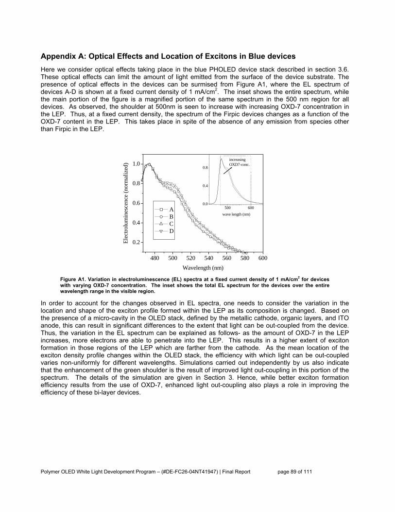
Polymer OLED White Light Development Program – (#DE-FC26-04NT41947) | Final Report page 89 of 111
Appendix A: Optical Effects and Location of Excitons in Blue devices Here we consider optical effects taking place in the blue PHOLED device stack described in section 3.6. These optical effects can limit the amount of light emitted from the surface of the device substrate. The presence of optical effects in the devices can be surmised from Figure A1, where the EL spectrum of devices A-D is shown at a fixed current density of 1 mA/cm2. The inset shows the entire spectrum, while the main portion of the figure is a magnified portion of the same spectrum in the 500 nm region for all devices. As observed, the shoulder at 500nm is seen to increase with increasing OXD-7 concentration in the LEP. Thus, at a fixed current density, the spectrum of the Firpic devices changes as a function of the OXD-7 content in the LEP. This takes place in spite of the absence of any emission from species other than Firpic in the LEP.
480 500 520 540 560 580 600
0.2
0.4
0.6
0.8
1.0
500 6000.0
0.4
0.8
A B C D
Elec
trolu
min
esce
nce
(nor
mal
ized
)
Wavelength (nm)
increasingOXD7-conc.
wave length (nm)
Figure A1. Variation in electroluminescence (EL) spectra at a fixed current density of 1 mA/cm2 for devices with varying OXD-7 concentration. The inset shows the total EL spectrum for the devices over the entire wavelength range in the visible region.
In order to account for the changes observed in EL spectra, one needs to consider the variation in the location and shape of the exciton profile formed within the LEP as its composition is changed. Based on the presence of a micro-cavity in the OLED stack, defined by the metallic cathode, organic layers, and ITO anode, this can result in significant differences to the extent that light can be out-coupled from the device. Thus, the variation in the EL spectrum can be explained as follows- as the amount of OXD-7 in the LEP increases, more electrons are able to penetrate into the LEP. This results in a higher extent of exciton formation in those regions of the LEP which are farther from the cathode. As the mean location of the exciton density profile changes within the OLED stack, the efficiency with which light can be out-coupled varies non-uniformly for different wavelengths. Simulations carried out independently by us also indicate that the enhancement of the green shoulder is the result of improved light out-coupling in this portion of the spectrum. The details of the simulation are given in Section 3. Hence, while better exciton formation efficiency results from the use of OXD-7, enhanced light out-coupling also plays a role in improving the efficiency of these bi-layer devices.

Polymer OLED White Light Development Program – (#DE-FC26-04NT41947) | Final Report page 90 of 111
Appendix B: Effect of Charge Balance and Micro-cavity Fig. B1 shows the structure of the devices used in this study. The light emitting polymer layer (LEP) in these PHOLEDs are comprised of polyvinylcarbazole (PVK) as the hole transporting matrix, 1,3,4-oxadiazole, 2,2'-(1,3-phenylene)bis(5-(4-(1,1-dimethylethyl)phenyl) or OXD-7 as an electron transporter and the blue phosphorescent dye Firpic (see section 3.10) amount of Firpic in the LEP is kept constant at 10% by weight, while the relative concentrations of PVK and OXD-7 are changed in order to vary the hole and electron transport within the LEP.
Figure B1: Device structure and composition of the LEP.
The actual composition of the LEP along with device labeling is clarified in Figure B1, which also shows the device architecture. Both PEDOT and the LEP are deposited sequentially by spin coating on indium tin oxide (ITO) coated glass substrates, followed by thermal evaporation of the cathode layers comprising CsF and Al. The LEP (thickness of 75nm) is spin coated from chlorobenzene and is baked at 80oC for 30min before deposition of cathode layers. As the final step, the devices are encapsulated before characterization. All device fabrication steps after PEDOT spinning until device encapsulation are carried out in an inert atmosphere.
Appendix B.2 Micro-cavity Theory and Optical Modeling
Optical simulation of the experimental results was performed using the micro-cavity simulation tool UniMCO 4.0 by UniCAD [16]. The method used in UniMCO is based on the transfer matrix formalism including additional source terms for electric field (i.e. the dipole emission terms). The electric field emitted by electric dipoles can be expressed in terms of superposition of s-(TE) and p-(TM) polarized waves, while the dipole source can be decomposed into three orthogonal components (ds, dp, dv), where ds and dp are in-plane dipole components, and dv is the out-off plane component. It can be shown that the powers per solid angle θ and surface emitted by such dipoles in unbounded medium of refractive index nemit are of the form:
π83
0 =sP
(1a)
θ
π2
0 cos83
=pP
(1b)
θ
π2
0 sin83
=pP
(1c)

Polymer OLED White Light Development Program – (#DE-FC26-04NT41947) | Final Report page 91 of 111
For a sheet of dipoles at distance z from the cathode-reflector, the power per unit solid angle and surface vps
frontP ,,
radiated outside the micro-cavity by the s-, p- and v-dipoles can be calculated from the following equations:
s
iss
siss
front Perr
rerP
I
02221
222
11
11
ϕ
ϕ
−
−+=
(2a)
p
ipp
pipp
front Perr
rerP
I
02221
222
11
11
ϕ
ϕ
−
−+=
(2b)
v
ivv
vivv
front Perr
rerP
I
02221
222
11
11
ϕ
ϕ
−
−+=
(2c)
Where r1 is the reflectivity coefficient of the anode mirror and r2 the reflectivity of the cathode mirror of the micro-cavity, ϕ and ϕ I are given by:
emitemit
I nz θλπϕ cos2
=
(3)
emitemit
I nd θλπϕ cos2
=
(4)
Where is the wave length of the emitted light and d is the optical path length, which can be expressed, taking into account penetration depth into the dielectric mirror and the effect of the phase change at the metal/organic interface, by
λπϕλ42
m
iii
eff dnn
nd ++⎟⎟
⎠
⎞⎜⎜⎝
⎛∆
= ∑
(5)
Where the first term is the penetration depth into the dielectric stack, neff is the refractive index for the stack, ∆n is the difference between the higher and lower indices of the stack, ni and di are the refractive index and the thickness of organic layers and ITO layer, and ϕm is the phase change at the metal mirror.
When the light impinges onto a metal surface the phase change ϕm between the incident and the reflected lights is given by:
20,2tan 2
02
121
101 πϕϕ ≤≤⎟⎟⎠
⎞⎜⎜⎝
⎛−+
= −mm nkn
kn
(6)
Where n1 - ik1 is the complex refractive index of the metal and n0 is the refractive index of the incident medium (organic dielectric). In the case of the devices used in this study n0 is equal to nemit.
Only the power (or EL) emitted in the source medium (refractive index nemit) with angles θemit smaller than
the critical angle: )(arcsin0
emita
nn
emit =θ, where na is the refractive index of the outside medium, can be
extracted out of the micro-cavity. The interval [ ]0,0 emitθ corresponds to the escape window of the emission.

Polymer OLED White Light Development Program – (#DE-FC26-04NT41947) | Final Report page 92 of 111
If 0
emitemit θθ > , the light will undergo total internal reflection. The amount of extracted light is a fraction of the light generated in a distance z from the cathode:
0,,,, 0 emitemitvps
frontvps
extr forPP θθ ≤≤= (7)
Considering an emission zone profile E(z) (0< z < Z), the total power radiated out of the device is given by
∫ ∫ ∫∞
=Z
vpsfront
vpstotal
emit
PdddzzEP0 0 0
,,,,
0
),(sin)(θ
λθλθθ
(8)
Further refinements are based on the optical constants as a function of wavelength for all layers of the device stack.
Considering eq.1 to 8, it is obvious, that the variation in the location and shape of the exciton profile formed within the LEP can result in significant differences in the extent to which light can be out-coupled from the device due to the presence of a micro-cavity in the OLED stack. It has been demonstrated that such micro-cavity effects can lead to changes in the electro luminescence (EL) spectrum, as light corresponding to different wavelengths are out-coupled to a different extent for a given location of the emission zone.
Furthermore the simulation tool allows determining the spectrum EL0, which is defined as the emission spectrum of the emitter in a space filled with the emitting medium without any interfaces. EL0 is extracted from experimental data (EL-spectrum of the device measured in the direction normal to the device substrate) by numerical back calculation based on the model described above.
Appendix B.3 Results and Discussion
In Figure B2, the luminance efficiency of the devices used in this study is plotted as a function of current density in the devices. Device efficiency is observed to rise with increasing OXD-7 concentration in the LEP between devices A-D.
10-3 10-2 10-1 100 1010
5
10
15
20
25
Device A B C D E
Current density (mA/cm2)
Lum
inan
ce e
ffic
ienc
y (c
d/A
)
Figure B2: Luminance efficiency of the devices used in this study plotted as a function of current density.
The improvement in device efficiency with increasing OXD-7 concentration is due to better electron transport in the device. As a reason for the drop in efficiency from device D to E, we assume that the optimum in charge balance is reached in device D and the charge transport in device E is already electron dominant.

Polymer OLED White Light Development Program – (#DE-FC26-04NT41947) | Final Report page 93 of 111
However this explanation does not also consider the optical effects taking place in the device stack, which limit the amount of light emitted from the surface of the device substrate. The EL spectra of devices A-E (Figure B3) proof the presence of optical effects in the devices. The spectra were measured at a fixed current density of 1 mA/cm2.
480 500 520 540 560 5800.0
0.2
0.4
0.6
0.8
1.0
400 500 600 7000.0
0.2
0.4
0.6
0.8
1.0
A B C D E FIT
Elec
trolu
min
esce
nce
(nor
m.)
wavelength (nm)
increasingOXD7-conc.
wave length (nm)
Figure B3: Measured EL-spectra of the devices A-E and simulation fit.
The inset shows the entire spectrum, while the main portion of figure B3 is a magnified portion of the same spectrum in the 500 nm region for all devices. As observed, the shoulder at 500nm is seen to increase with increasing OXD-7 concentration in the LEP. Thus, at a fixed current density, the spectrum of the Firpic devices changes as a function of the OXD-7 content in the LEP. This takes place in spite of the absence of any emission from species other than Firpic in the LEP.
In order to account for the changes observed in EL spectra, one needs to consider the variation in the location and shape of the exciton profile formed within the LEP as its composition is changed.
Using the optical simulation tool described above, the EL spectra in Fig. B3 was fitted. In a first step the spectrum EL0 was calculated based on the measured EL spectrum of device A. For the calculation the location of the EMZ is needed. Here, we have defined the location of the EMZ as the distance between the cathode and the centre of a Gaussian distribution of excitons within the light emitting polymer with a full width at half maximum (FWHMEMZ) of 20 nm [17]. The distance between the EMZ and the cathode was varied to fit the PL-spectrum of the LEP used in the device by the calculated EL0. Using the spectrum EL0 extracted from the measured EL-spectrum of device A, the measured EL-spectra of the devices B, C, D and E were fitted by varying the location of the EMZ. According to the simulation the distance between cathode and EMZ increased from 20 nm for device A to 60 nm for device E. This can be explained as follows: As the amount of OXD-7 in the LEP increases, more electrons are able to penetrate into the LEP. This results in a higher extent of exciton formation in those regions of the LEP which are farther from the cathode.
This change in the location of the EMZ affects the external device efficiency. In the following, we quantify the effect due improved charge balance and the optical effect due to the change in the location of the EMZ on the resulting device efficiency. Using the simulation tool the external light output (for constant current density) as a function of the location of the EMZ was calculated (Figure B4). Here, the internal quantum efficiency was assumed to be constant.

Polymer OLED White Light Development Program – (#DE-FC26-04NT41947) | Final Report page 94 of 111
10 20 30 40 50 60 70
0.6
0.8
1.0
1.2
1.4
1.6
1.8
2.0
2.2E'D'C'
B'
A'
light
tout
put (
norm
.)
distance cathode-EMZ (nm) Figure B4: Simulation of the external light output (for constant current density) as a function of the location of the EMZ for the imaginary devices A’, B’, C’, D’, E’.
The circles in Figure B4 mark the light output for the imaginary devices A’, B’, C’, D’, E’, which all have the same locations of the EMZ as the corresponding devices A, B, C, D, E. The data was normalized on the light output of device A’. The location of the EMZ of device D and D’ is the optimum regarding efficiency improvement due to the micro-cavity effect. The graph in Figure B4 describes the efficiency improvement in comparison to device A due to the optical effect dependent on the location of the EMZ. For the real devices A, B, C, D, E the internal quantum efficiency was changed due to the effect of OXD7 concentration on charge balance. The improvement in internal efficiency in comparison to device A is given by:
)(
)'(')()(1 AO
XOXOX m −=∆
(9)
Where )(XOm ( ],,,[ EDCBX ∈ ) is the measured light output at constant current density and )'(' XO (
]',',','[' EDCBX ∈ ) is the light output of the imaginary devices normalized on the output of A’. The improvement compared to device A due to the micro-cavity effect is given by:
))(()()( 12 AOXOX mm +∆−=∆ (10)
The block graph in Figure B5 shows the external light output of the devices used in this study normalized on the output of device A (current density J= 1 mA/cm2). The cross hatched area represents the efficiency improvement compared to device A due to the micro-cavity effect. The improvement in internal device efficiency is marked by the double ended arrows.

Polymer OLED White Light Development Program – (#DE-FC26-04NT41947) | Final Report page 95 of 111
0 10 20 30 400123456789
10
∆1
A DCB E
light
out
put (
norm
.)
OXD7 conc. [%]
+ = measured light output improvement due to cavity effect ∆2
Figure B5: The external light output of the devices used in this study normalized on the output of device A. The cross hatched area represents the efficiency improvement compared to device A due to the micro-cavity effect. The improvement in internal device efficiency is marked by the double ended arrows.
Both, the efficiency improvement due to the micro-cavity effect and the improvement due to the effect of OXD7 increase from device A to device D. The drop of device efficiency from device D to device E is mainly caused by a decrease in internal device efficiency. Here we assume that the optimum in charge balance is reached for device D and the charge transport in device E is already electron dominant.
In the following the accuracy in the separate quantification of the efficiency improvement due to charge balance and the improvement due to the change in the location of the EMZ is discussed. The calculation of this quantitative separation was based on a FWHMEMZ of 20 nm for the imaginary devices A’, B’, C’, D’, E’. Varying the values of the FWHMEMZ in the range between 5 nm and 40 nm, the corresponding EL-spectra of the devices A’, B’, C’, D’, E’ were obtained by simulation. For each device no significant difference in the slope of the EL-spectrum was observed, when changing the FWHMEMZ. Thus, the measured EL-spectra of the real devices A, B, C, D, E can be fitted assuming values of the FWHMEMZ in the range between 5 nm and 40 nm. Furthermore, the external light output of the imaginary devices A’, B’, C’, D’, E’ was simulated as a function of the FWHMEMZ. For device B’ and C’ the output was calculated in the range from 5 nm to 40 nm (Fig. B6).

Polymer OLED White Light Development Program – (#DE-FC26-04NT41947) | Final Report page 96 of 111
0 5 10 15 20 25 30 35 40
1.0
1.2
1.4
1.6
1.8
2.0
O'min(B')
O'max(B')
light
out
put (
norm
.)
full width at half maximum (nm)
Device: A' B' C' D' E'
Figure B6: external light output of the imaginary devices A’, B’, C’, D’, E’ as a function of the FWHMEMZ.
For the device A’, D’, E’ the range was limited to values smaller than 40 nm, since the location of the EMZ is closer to the border of the LEP. In the graph in Fig. B5 for each of the devices B’, C’, D’, E’ a minimum and
a maximum light output ( )'('min XO and )'('max XO , ]',',','[' EDCBX ∈ ) is given. The error in the
calculation of the improvement in internal efficiency in comparison to device A can be calculated based on )'('min XO and
)'('max XO according to equation 9. A comparison of the magnitude of the error to the measured light output (Figure B5) proofs the significance in the quantitative separation of the two effects.

Polymer OLED White Light Development Program – (#DE-FC26-04NT41947) | Final Report page 97 of 111
Appendix C: General Method to Evaluate Substrate Surface Modification Techniques for Light Extraction Enhancement of OLEDs Using the approaches of scheme (1) and (2) (ref. introduction 3.13), the waveguided light retained within the substrate of the unmodified device (standard flat glass substrate) is extracted. The improvement in light outcoupling by various methods of modifying the substrate surface is often quantified by an apparent enhancement factor, k = η2/η1, where η1 is the efficiency of the unmodified OLED and η2 is the efficiency of the device after modifying the substrate.
In this study we showed a strong dependence of the enhancement factor k on the device architecture itself. Furthermore we demonstrated an alternative method to determine the enhancement of light extraction using light outcoupling approaches of scheme (1) or (2) discussed earlier. The proposed method thus eliminates dependence on device architecture which would otherwise lead to inaccurate conclusions regarding the efficiency of the device itself.
Appendix C.2 Fabrication of OLEDs
Fig. C.1 shows the structure of the green emitting OLEDs (peak wavelength = 510 nm) used in this study. Each substrate has 4 individual OLEDs with a 0.4 cm2 active area. The glass substrate has a thickness of 0.7 mm and a refractive index n = 1.52.
ITO (130 nm)
Glass Substrate (n = 1.52, 0.7 mm)
PEDOT (60 nm)
EML (70 nm)
PBD (10 nm)
Alq3 (0, 10, 30, 50, 70 nm)
CsF (1 nm)
Al (200 nm)
Brightness Enhancement Film
Figure C.1: Structure of the green emitting OLEDs used in this study.
The OLEDs are fabricated as follows. Indium tin oxide (ITO) coated glass substrates were patterned using standard photolithographic techniques. This was followed by cleaning of the ITO surface including wash steps with DI water. In addition, the ITO substrates were subjected to oxygen plasma treatment for 10 minutes. A thin (60 nm) film of poly(3,4)-ethylendioxythiophene doped with poly(styrene sulfonate) (PEDOT:PSS) was spin coated atop the ITO and then baked for 30 min at 200 °C. The green emitting layer (EML) was then spin coated on the top of the PEDOT:PSS with conditions to yield a light emitting layer thickness of around 70 nm. The light emitting layer was then annealed at 80 C for 30 min. The solution for the EML consisted of 24 % wt 2-(4-biphenyl)-5-(4-tert-butylphenyl)-1,3,4-oxadiazole (PBD) , 9% wt 4,4'-bis(m-tolylphenylamino)biphenyl (TPD), 6 % wt fac-tris(2-phenylpyridine)iridium Ir(ppy)3 and 61 % wt polyvinylcarbazole (PVK) in chlorobenzene [5]. On the top of the EML a hole-blocking layer consisting of 2-(4-biphenyllyl)-5-(4-tert-butylphenyl)-1,3,4-oxadiazole (PBD) was thermally evaporated in a vacuum coater to a thickness of 10 nm. This was followed by thermal evaporation of a tris(8-hydroxyquinoline) aluminum (Alq3) layer on top of the PBD layer. Devices with five different Alq3-layer thicknesses (0 nm, 10 nm, 30 nm, 50 nm, 70 nm) were prepared. Then a cesium fluoride (CsF) layer with a thickness of 1 nm was deposited

Polymer OLED White Light Development Program – (#DE-FC26-04NT41947) | Final Report page 98 of 111
as an electron injection layer. Finally an Al layer with a thickness of 200 nm was deposited as the cathode. All the thermally evaporated layers were deposited in a vacuum coater sequentially in a single pump down cycle. Following evaporation of the cathode, the devices were encapsulated with a glass lid and getter. All device fabrication steps from the EML spin coating to device encapsulation were carried out in an inert nitrogen atmosphere.
Appendix C.3 Brightness Enhancement Film
After measuring the light output of the unmodified devices (the method is described in more detail below), a Brightness Enhancement Film (BEF) prepared from 3M (Vikuiti BEF II 90/50) was applied on the surface of the devices. The BEF film consists of an acrylic resin with prismatic features on its surface coated on a polyester substrate. The prism angle is 90° and the prism pitch is 50 µm. The BEF film has a nominal thickness of 155 µm and was optically coupled to the glass substrate with optical laminating tape (3M No. 8141, n = 1.49).
Appendix C.4 Measurement of Substrate Mode and External Mode Intensity
The OLED emission intensity was measured using a large area (18 mm X 18 mm) Si photodiode according to a method described by Nakamura [15]. The distance between the Si photodiode and the OLED substrate’s surface was kept at <0.5 mm. Measurements were carried out alternatively with an air gap and an optical gel whose refractive index was 1.56. When the air gap was filled with gel, TIR at the glass/air interface disappeared, enabling the emitted light of the external and substrate waveguided modes to be measured by the Si photodiode simultaneously. Thus three intensities Iair, Igel and Ifilm were measured, where Iair and Igel were the emission intensity detected by the Si photodiode at the air and gel gaps before modifying the device, and where Ifilm was the emission intensity detected at the air gap after applying the BEF film. All intensities were measured at a current density of 1 mA/cm2.
Appendix C.5 Results and Discussion
Fig. C.2 shows the external light output of the devices before and after applying the BEF film as a function of the Alq3 thickness. It is observed that with increasing Alq3 thickness the light output in both cases (i.e., without and with the BEF film) decreases. However, the effect of light out-coupling enhancement due to the BEF film is increased. This enhancement is calculated and the results are shown in table C.1, where the values of k (given by k = Ifilm/Iair) are listed.
1 2 3 4 50.0
0.5
1.0
1.5 without BEF with BEF
30 7050100
Inte
nsity
(nor
m.)
Thickness of Alq3 layer [nm]
Figure C.2: Light output of the devices before and after applying the Brightness Enhancement Film. The intensities are normalized on the output of the light output of the device with an Alq-layer thickness of 10 nm. The error bars represent the standard deviations of the measured values.

Polymer OLED White Light Development Program – (#DE-FC26-04NT41947) | Final Report page 99 of 111
Alq layer thickness [nm] k = Ifilm/Iair
0 1.30
10 1.27
30 1.80
50 2.04
70 2.25
Table C.1. Factor of absolute light out-coupling enhancement k.
The enhancement factor k has a strong dependence on the device structure itself, which can be explained by optical theory. Therefore the EL-pattern in the micro-cavity was calculated for the devices used in the study by the means of the simulation tool described above. Here we define the EL pattern as the power per unit solid angle radiated outside the micro-cavity integrated over all wavelengths. Fig. C.3 shows the EL pattern (the power per unit solid angle radiated outside the micro-cavity) integrated over all wavelengths for different Alq3 thicknesses. The angle of 0° corresponds to the direction normal to the substrate, where the angle of 90° corresponds to the direction parallel to the substrate. With increasing values of Alq3 layer thickness the distribution of intensity is shifted to higher angles with respect to the normal of the substrate (0°). Without substrate surface modification, the light at the radiation angle below 1 escapes from the device as an external mode, that between θ1 and θ2 gets trapped in the glass as a substrate wave-guided mode, and that above θ2 is coupled into the ITO layer as a result of anode/organic wave-guiding. As the intensity distribution shifts to higher angles, there will be an increase in light losses within the unmodified substrate due to TIR.
Figure C.3: Normalized EL pattern of the devices used in this study (integrated over all wavelengths)
In the case of unmodified devices, with increasing Alq3 layer thickness, the fraction of substrate wave-guided light compared to the fraction of the external light output increases as a result of the shift of the EL pattern to higher angles (Fig. C.3). Only the photons, which are emitted by the EML in a lower angle, defined by the escape cone of the substrate are extracted out of the device. After applying the BEF film, photons of higher emission angles can be extracted due to the prismatic structure of the film. The higher the fraction of substrate wave-guided light the stronger is the light out-coupling enhancement of the BEF film. Thus, the light out-coupling enhancement obtained by calculating the ratio between the light output of the surface modified and the output of the unmodified device by itself does not lead to accurate conclusions about the effectiveness of the light out-coupling method.
Here, we propose a more accurate method to valuate the light out-coupling enhancement due to substrate surface modification. Therefore we need the intensity Igel. Fig. C.4 shows the measured intensities Iair and Igel, which were measured as a function of the Alq3 layer thickness. The intensity Iair, which is equal to the light output of the device before applying the BEF film, decreases with increasing values of Alq3 layer

Polymer OLED White Light Development Program – (#DE-FC26-04NT41947) | Final Report page 100 of 111
thickness to 1/3 of the output of the device without Alq3. With increasing Alq3 layer thickness the intensity Igel, which is related to the sum of the external light output and the substrate wave-guided light, decreases to 2/3 of the value for the device without Alq3. Quasisinusoidal variation of current efficiency vs. Alq3 thickness is attributed to the interference effect between direct emission and emission reflected from the metallic mirrors of the electrodes.
0 10 20 30 40 50 60 700.0
0.5
1.0
1.5
2.0
2.5
Iair Igel
Inte
nsity
(nor
m.)
Alq3 layer thickness [nm]
Figure C.4: The emission intensities detected by the Si photodiode at the air and gel gaps before substrate surface modification of the devices. The intensities are normalized on the output of the light output of the device with a Alq-layer thickness of 10 nm. The error bars represent the standard deviations of the measured values.
The performance of the BEF film can be determined by considering the ratio between the external outputs of the BEF film laminated device and the total amount of light, which is measured with the gel. This ratio is given by Ifilm/Igel and is approximately constant (Ifilm/Igel ≈ 0.6) for all device structures (table 4). By the means of the BEF film about 60 % of the light, which is coupled into the substrate, is extracted out of each modified device.
Alq3 layer thickness (nm) Ifilm/Igel
0 0.63
10 0.60
30 0.63
50 0.60
70 0.58
Table C.2: Ratio between outputs of surface modified device and light intensity coupled into the substrate (Ifilm/Igel)
In conclusion we have demonstrated that the apparent effectiveness of light out-coupling enhancement using a method of modifying the substrate surface is significantly dependent on the device structure itself. This apparent effectiveness however is not the correct value to judge the effectiveness of a technique to enhance light out-coupling due to substrate surface modification. The ratio between the light output of the surface modified device and the total amount of light which is generated in the device stack and coupled into the substrate(before the substrate/air interface), is a more accurate parameter to describe the light enhancement properties. In the optimal case the ratio is 1, which corresponds to a light out-coupling methodology completely suppressing substrate wave guiding. Determination of the enhancement properties using the proposed method not only allows the comparison of different methods of substrate surface modifying techniques, but also provides an analytical understanding to enable further improvement of each technique.

Polymer OLED White Light Development Program – (#DE-FC26-04NT41947) | Final Report page 101 of 111
Appendix D: Improving Emission Rate The incorporation of metallic nano-particles into organic host materials, resulting to a new class of materials combining inorganic and organic constitutes (hybrid materials), it’s a topic which attract current interest from the research community [18].
The recent development of metal nano-particles with plasmon derived optical response can be used to further improve the performance of OLEDs. It is believed, that in the case of fluorescence based organic light emitting diodes, incorporation of metal nano-particles within the light emitting layer can be used to quench triplet non-radiative excited states and thus suppress photo-oxidation and enhances luminance stability of fluorescence based OLEDs [19]. Other published literature suggests that acceleration of the radiative processes can be achieved by incorporation of metal nano-particles within the light emitting layer of phosphorescence or fluorescence based OLEDs [20]. The acceleration of the radiative processes is achieved by the interaction of the light emitting species with surface plasmon resonances in the vicinity of metal nano-particles. In all of the above approaches, metal nano-particles were blended to the emissive layer of the OLEDs [19,20].
However, direct incorporation of metal nano-particles into the active region or other layers within the OLED can cause additional negative effects. For example, it has been demonstrated that incorporation of a gold nano-particle even at low volume fraction of 3 x 10⁻⁵ within a light emitting fluorescence polymer layer, introduces strong hole blocking effects and a large increase in operating voltage [21]. Furthermore, incorporation of metal nano-particles in the active region of both fluorescence-based and phosphorescence-based OLEDs is likely to quench emission, due to Forster-type energy transfer between the emitter and the metal nano-particle, and thus can strongly deteriorate device performance. Encasing nano-particles in organic capping molecules is suggested to achieve an optimum balance between quenching and acceleration of the radiative processes of the emissive states. A nearly two fold increase of luminance efficiency of slow phosphorescence (2,3,7,8,12,13,17,18-Octaethyl-21H,23H-porphine platinum (II) based OLEDs (around 10 microsecond emission lifetime) has been reported by blending into the phosphorescence LEP thiol-capped gold nano-particles [20]. However accelerating the radiative properties of faster phosphorescence emitters such as the currently used Iridium based compounds with 1 microsecond emission lifetime, is not straightforward and capping of the metal nano-particles is not a well known procedure.
We demonstrate improvement in the performance of Tris(2-4(4-toltyl)phenylpyridine)iridium Ir(mppy)3 electrophosphorescence based organic light emitting diodes (PHOLEDs) by conditioning the interface between Poly(3,4-ethylenedioxy thiophene):poly(styrene sulfonate) (AI4083, PEDOT:PSS) buffer layer and the phosphorescence based light emitting layer (LEP) with gold nanoparticles.
The optical absorption band of the gold nanoparticles with a diameter of 1-10 nm dispersed in toluene is located in a broad region between 500 and 550 nm which overlap with the energy level of the triplet excitons of Ir(mppy)3 at 508 nm. Thus gold nanoparticles are particularly suitable to be incorporated in the interfaces of a phosphorescence OLED since they display a pronounced surface plasmon resonance in the visible region of the spectrum close to the emission band of the Ir(mppy)3 triplet emitter. The diode architectures studied are described as follows. The control diode is based on ITO/PEDOT:PSS/ LEP/CsF/Al. CsF/Al is the preferred cathode in such type of devices, it has been previously reported that CsF improves electron injection. The device incorporates gold-nanoparticles between the LEP layer and the cathode is based on ITO/ PEDOT:PSS/Gold-nanoparticles/ LEP / CsF/Al. The LEP for all the devices studied contains [61% PVK + 24% PBD + 9% TPD + 6% Ir(mppy)3]. The concentrations are given by weight. Figure D.1 is a schematic representation for the device structure incorporating gold nano-particles.

Polymer OLED White Light Development Program – (#DE-FC26-04NT41947) | Final Report page 102 of 111
Figure D.1: The device structure incorporating metal nano-particles in the interface between buffer layer and the phosphorescence based light emitting layer.
Figure D.2 shows the current density/ voltage (J-V) properties (main plot) and the luminance-voltage properties (inset plot) of the devices under study. From the J-V and luminance-voltage characteristics it is clear that the current density and luminance is lower through the whole voltage range for the device incorporating gold nanoparticles in the interface between PEDOT:PSS and LEP compare to control device. This indicates a higher driving voltage for the devices incorporating the gold nano-particles. It is clear that incorporation of gold nanoparticles in the interface between buffer layer and LEP degrading the hole injection properties of the phosphorescence OLED.
0 2 4 6 80
2
4
6
8
0 2 4 6 80
500
1000
1500
Control Device Device with gold-nanoparticles
Brig
htne
ss(c
m/m
2 )
Voltage (V)
Cur
rent
den
sity
(mA
/cm
2 )
Voltage (V)
Lum
inan
ce (c
d/m
2 )
Figure D.2: Main plot: Current density-voltage characteristics of the phosphorescence OLEDs under study. The control device is represented with open squares, the devices incorporating gold nano-particles in the interface between buffer layer and LEP represented with solid squares.
Figure D.3 shows the luminance efficiency versus current density properties for the devices under study. The peak luminance efficiency of the control device reaching 27 cd/A. Devices with incorporated gold nanoparticles in the interface between PEDOT:PSS and LEP exceeding 36 cd/A. This is a 33 % improvement in luminescence efficiency for the device incorporating metal nanoparticles.
Buffer layer
Glass/ITO
Light emitting layer
Cathode

Polymer OLED White Light Development Program – (#DE-FC26-04NT41947) | Final Report page 103 of 111
The strong enhancement in the luminance efficiency for the phosphorescence devices incorporating gold nano-particle in the interface between LEP and adjacent layers is a product of an increased radiative decay rate. The radiative decay of Ir(mppy)3 is accelerated by incorporation of gold-nanoparticle in the interface between LEP and adjacent layers. The improvement in the emission rate is attributed to modification in the local density of states caused via an interaction of the phosphorescence emitter with the metal nano-particles surface plasmons [20,22].
-200 0 200 400 600 800 1000 1200 1400-5
0
5
10
15
20
25
30
35
40
Lum
inan
ce E
ffici
ency
(cd/
A)
Luminance(cd/m2)
Control Device Device with gold nanopartcles
Figure D.3: Luminance efficiency-luminance characteristics of the phosphorescence OLEDs under study. The control device is represented with open squares, the devices incorporating gold nano-particles in the interface between buffer layer and LEP represented with solid squares.
Figure D.4 shows the luminous efficacy (power efficiency) versus applied voltage for the devices under study. Due to improved quantum efficiency and despite the retardation in the hole injection properties increasing the operation voltage, device with gold nano-particles show higher peak luminance efficacy of 16 lm/W compare to a value of 13 lm/W observed for the control devices.

Polymer OLED White Light Development Program – (#DE-FC26-04NT41947) | Final Report page 104 of 111
0 2 4 6 8 100
5
10
15Lu
min
ous
Effic
acy
(lm/W
)
Voltage (V)
Control Device Device with gold nanopartcles
Figure D.4: Luminance efficiency-voltage characteristics of the phosphorescence OLEDs under study. The control device is represented with open squares, the devices incorporating gold nano-particles in the interface between buffer layer and LEP represented with solid squares.
We note that device structures using the same phosphorescence LEP used here with low conductivity CH8000 PEDOT:PSS reported above, produce more efficient phosphorescence OLEDs compared to the higher conductivity AI4083 PEDOT:PSS. However, incorporation of gold nano-particles in the interface between the CH8000 buffer layer and LEP, with the conditions described above did not show clear improvement in the device performance. The experimental conditions for incorporating metal nano-particles in the interface of OLEDs can alternatively be described as a method to treat the surface of organic layers with metal-nanoparticles, thus the processing conditions should be re-optimized according to the surfaces under treatment.
In summary, we demonstrated a 33 % improvement in luminance efficiency in phosphorescence based OLEDs by incorporation of metal nano-particles in the interface between the light emitting layer and adjacent layers. The improvement originates by acceleration of emission rates caused by the interaction of the phosphorescence emitting species with the metal nano-particle surface plasmons (this has not been proven here, one could argue that the effects are due to a more optimized balance transport as a result of the nanoparticle incorporation). We believe that a more intimate interface between metal nano-particles and light emitting layer can achieved by optimizing the processing conditions. This will also result to a stronger improvement of the luminous efficacy (power efficiency) of phosphorescence based OLEDs.

Polymer OLED White Light Development Program – (#DE-FC26-04NT41947) | Final Report page 105 of 111
List of Figures Figure 1.1: Image of a 6”x10” demonstrator, along with a 3”x5” demonstrator from first year................7
Figure 1.2: Image of an inkjet printed 3”x5” color tunable demonstrator.................................................7
Figure 2.1: Inter-connected glove boxes; used for fabricating multiple small area OLED device for
materials characterization and device testing. ......................................................................9
Figure 2.2: Photolithography 200 mm line............................................................................................ 10
Figure 2.3: Polymer coating, cathode evaporation and encapsulation 200 mm line............................ 11
Figure 2.4: Tepla 4011 Plasma tool (top); Litrex 140P industrial inkjet printer (bottom). ..................... 11
Figure 2.5: Infra-red imaging system (left) and Luminance Lifetime measurement system (right) used
for reliability testing............................................................................................................. 12
Figure 3.1: EL spectra of various OLED device structures and their corresponding CRI values. ....... 14
Figure 3.2: J-V characteristics of three polymers with varying compositions....................................... 15
Figure 3.3: Energy level diagram illustrating electron trapping by red and green emitters. ................. 16
Figure 3.4: J-V of blue and white polymer devices............................................................................... 17
Figure 3.5: The HOMO and LUMO energy levels of TFB used for interfacial layers and Ir(mppy)3, PVK,
TPD, PBD components of the LEP compared to the work function of PEDOT:PSS (all
referenced with respect to vacuum). The vector in the scheme indicates the direct injection
from the TFB interfacial layer into Ir(mppy)3 phosphorescence organo-metallic compound
within the LEP. ................................................................................................................... 20
Figure 3.6: Left plot: Current density-voltage characteristics of the solution processed
electrophosphorescence OLEDs under study. Right plot: Luminance-voltage characteristics
of the solution processed electrophosphorescence OLEDs under study. The control device
is represented with open squares, the devices incorporating a TFB and PFO interfacial
layer between PEDOT:PPS represented with solid squares and solid circles respectively.
For all cases the light emitting layer contains [61% PVK + 24% PBD + 9% TPD + 6%
Ir(mppy)3]. .......................................................................................................................... 21
Figure 3.7: Left plot- Luminance efficiency-current density characteristics of the solution processed
electrophosphorescence OLEDs under study. Right plot: Luminous efficacy- current density
characteristics of the solution processed electrophosphorescence OLEDs under study. The
control device is represented with open squares, the devices incorporating a TFB and PFO
interfacial layer between PEDOT:PPS represented with solid squares and solid circles
respectively. For all cases the light emitting layer contains [61% PVK + 24% PBD + 9%
TPD + 6% Ir(mppy)3]. ........................................................................................................ 22
Figure 3.8: The device architecture for optimized charge injection. Incorporating an electron (PBD) and
hole (TFB) interfacial layers. The LUMO energy levels of PBD and the HOMO energy level

Polymer OLED White Light Development Program – (#DE-FC26-04NT41947) | Final Report page 106 of 111
of TFB are similar to that of the Ir(mppy)3 phosphorescence compound. The arrows in the
scheme indicates the electron/hole injection from the PBD/TFB interfacial layers into
Ir(mppy)3 phosphorescence compound............................................................................. 23
Figure 3.9: Left plot: Luminance efficiency-current density characteristics Right plot: luminous efficacy-
current density characteristics of the PHOLEDs under study. The control device is
represented with open squares, the devices incorporating a PBD electron injecting layer
represented with solid circles and the devices incorporating both PBD and TPD electron
and hole injecting layers respectively represented with solid squares and solid circles
respectively. ....................................................................................................................... 23
Figure 3.10: Luminance efficiency vs. current density and electroluminescence spectrum for the green
PHOLED under study......................................................................................................... 24
Figure 3.11: Luminance efficiency vs. current density and electroluminescence spectrum for the red
PHOLED under study......................................................................................................... 25
Figure 3.12: The table contains the device nomenclature based on the composition of the LEP. The
schematic shows the device architecture along with the distance between the emission
zone location (X) and the cathode. Also shown is the variation in current density vs.
voltage for the different devices. ........................................................................................ 25
Figure 3.13: Luminance efficiency (cd/A) versus current density for devices with varying OXD-7
concentration in the light emitting spin coated layer. The inset shows cd/A and luminous
efficacy (lm/W) data for device D plotted against of device luminance (cd/m2). Axes should
be labeled the same way in all figures. .............................................................................. 26
Figure 3.14: Luminance efficiency (cd/A) and luminous efficacy (lm/W) data versus current density for
the blue PHOLEDs incorporating TPTA............................................................................. 27
Figure 3.15: 20 lm/W single emitting layer cool white phosphorescence device. .................................. 28
Figure 3.16: Electroluminescence spectra of devices reported in this study. The spectra shaded grey
are for devices which contain 0.1% of the yellow dye while the un-shaded spectra are for
devices with 0.2% yellow dye............................................................................................. 29
Figure 3.17: Luminous efficacy (lm/W) performance of device D with a high CRI of 87........................ 30
Figure 3.18: Schemes of the 4 general approaches to generate white light based on organic light
emitting devices.................................................................................................................. 31
Figure 3.19: Excitation and emission spectrum of the nitridosilicate phosphor used in the down-
conversion layer. ................................................................................................................ 32
Figure 3.20: Normalized output spectrum of the white light emitting down-conversion device. The
spectrum was fitted according a simple down-conversion model, in order to calculate the
expected efficiency of the device without consideration of light extraction enhancement.
The picture shows the white light emitting device.............................................................. 32

Polymer OLED White Light Development Program – (#DE-FC26-04NT41947) | Final Report page 107 of 111
Figure 3.21: (a) EL-spectrum of bluish-green emitter. (b) Resulting output spectrum of the device. (c)
Absorption and re-emission spectra of the orange perylene dye. (d) Absorption and re-
emission spectra of the red perylene dye. ......................................................................... 35
Figure 3.22: The external mode, the substrate wave-guided mode and the anode/organic wave-guided
mode in an organic EL device. Dependent on the emission angle θ the generated photons
are out-coupled or wave-guided......................................................................................... 36
Figure 3.23: The external light output of the devices used in this study normalized on the output of
device A. The cross hatched area represents the efficiency improvement compared to
device A due to the micro-cavity effect. The improvement in internal device efficiency is
marked by the double ended arrows.................................................................................. 37
Figure 3.24: Light output of the devices before and after applying the Brightness Enhancement Film.
The intensities are normalized on the output of the light output of the device with an Alq-
layer thickness of 10 nm. The error bars represent the standard deviations of the measured
values. ................................................................................................................................ 38
Figure 3.25: Luminance efficiency-luminance characteristics of the phosphorescence OLEDs under
study. The control device is represented with open squares, the devices incorporating gold
nano-particles in the interface between buffer layer and LEP represented with solid
squares............................................................................................................................... 39
Figure 4.1: 200 x 200 mm substrate with six Year 1 lighting tiles (left) and details of the layout of the tile
(right). ................................................................................................................................. 41
Figure 4.2: Wavy pattern in luminance due to non-uniformity in the light emitting polymer layer (left).
Improved uniformity achieved by optimizing drying conditions (right). .............................. 42
Figure 4.3: Design for the 200 x 200 mm substrate with 42 Polaris lighting tiles (left) and detail of the
layout of the tile (right)........................................................................................................ 43
Figure 4.4: Efficiency and CRI as a function of OLED device structure............................................... 43
Figure 4.5: Lifetime of tiles from an initial luminance of 250 cd/m2. Tiles 1 and 3 developed shorts near
the end of the test............................................................................................................... 44
Figure 4.6: Efficiency performance of the green phosphorescent LEP on the Polaris design, fabricated
in the pilot line (need to label the y-axes)........................................................................... 44
Figure 4.7: Luminance decay (left) and voltage rise (right) for the green phosphorescent LEP
fabricated in the Materials and Device Line. ...................................................................... 45
Figure 4.8: Diffusion effects of Brightness Enhancement Film. ........................................................... 45
Figure 4.9: Luminance diffusing effects of Brightness Enhancement Film. ......................................... 46
Figure 4.10: Large area lighting panel consisted of 4x10 white emitting (LHS) and RGB emitting (RHS)
small tiles............................................................................................................................ 46
Figure 4.11: Exemplary cross section of an OLED device with particle contamination. ....................... 47
Figure 4.12: I-V curve comparison for two OLED lighting devices with and w/o leaky paths. ............... 48

Polymer OLED White Light Development Program – (#DE-FC26-04NT41947) | Final Report page 108 of 111
Figure 4.13: Correlation between IR intensity and leakage current. ...................................................... 48
Figure 4.14: Lifetime progression of white polymer OLED lighting device with and w/o leaky paths. ... 49
Figure 4.15: IR signature (bright spots) comparison of OLED lighting panel plates with different process
conditions. .......................................................................................................................... 49
Figure 5.1: Images of ink-jet printed color tunable tiles. The ink-jet printing head is also shown in the
figure................................................................................................................................... 52
Figure 5.2: CIE diagram showing the range of color tunability that can be achieved with the IJ printed
tiles ..................................................................................................................................... 52
Figure 5.3: 200 mm x200 mm plate with 6 tiles (left), and single tile showing the 96 columns and anode
and cathode contacts (right)............................................................................................... 53
Figure 5.4: Tepla 4011 Plasma tool (left), and Litrex 140P industrial inkjet printer (right). .................. 54
Figure 5.5: Optical micrograph of a printed PEDOT sample. The films are uniform and repeatable. The
graph on the right shows a Dektak profile of the film which confirms that the films are flat.55
Figure 5.6: PL image of printed inks. Inks were optimized for spin coating (left), and PL image of
printed inks. Inks were optimized for inkjet printing (right). ................................................ 56
Figure 5.7: Electroluminescence image of device made with inks optimized for spin-coating (left), and
Electroluminescence image of device made with inks optimized for IJ printing (right) ...... 56
Figure 5.8: Jetting stability of the PEDOT ink. PEDOT can be printed at high frequencies up to at least
7000 Hz (left), and Effect of the drive parameters for PEDOT. The pulse width should be
chosen to achieve maximum velocity (right). ..................................................................... 57
Figure 5.9: Shelf life studies of red ink. The viscosity of the ink is stable for several weeks. .............. 57
Figure 5.10: Developing a stable process window for the plasma process in San Jose (left) and
Uniformity of surface properties of across a 350mm x350 mm substrate using the new
Tepla plasma chamber (right). ........................................................................................... 58
Figure 5.11: Pictures showing optimization of drop position and thickness optimization (left), and optical
micrograph of a printed PEDOT sample. The films are uniform and repeatable (right). ... 59
Figure 5.12: PL (photoluminescence) image of lines printed with red LEP. LEP does not completely fill
the width of the line (left), and PL (photoluminescence) image of lines printed with green
LEP. LEP does not completely fill the ends of the line (right). ........................................... 59
Figure 5.13: Electroluminescence picture of a tile printed with the green polymer. Some defects are
clearly visible (left); and green tile with every third line addressed (right). ........................ 60
Figure 5.14: Current, Voltage, Luminance curve (left) and Efficiency vs. Voltage curves for green tile 60
Figure 5.15: Relative impact of various factors on the contact angles of PEDOT on ITO (left), and photo-
resist (right). ....................................................................................................................... 62
Figure 5.16: Schematic showing locations of contact angle measurements (left), and the actual contact
angle data (right). ............................................................................................................... 62
Figure 5.17: Figure showing the stability of the surface energy of ITO with time. ................................. 63

Polymer OLED White Light Development Program – (#DE-FC26-04NT41947) | Final Report page 109 of 111
Figure 5.18: Non-uniformity in electroluminescence due to drying stains.............................................. 63
Figure 5.19: Distribution of emission intensity in samples across a plate. ............................................. 64
Figure 5.20: Photoluminescence images showing pockets with mouse-bites (left), and pockets without
mouse-bites (right) printed with the new optimized process. ............................................. 64
Figure 5.21: Pictures of a pocket after the deposition of the liquid (left), and after the liquid dries into a
solid film (right). .................................................................................................................. 65
Figure 5.22: Picture showing bright spots due to the vacuum holes in the hot plate. ............................ 65
Figure 5.23: EL picture showing poor fill factor (left), and EL picture with improved fill factor (right). ... 66
Figure 5.24: Summary of the performance of devices made with different inks. ................................... 66
Figure 5.25: Images of electroluminescence from tiles made with IJ printing........................................ 67
Figure 5.26: Images showing the demonstrators made with the tunable R,G,B light source. ............... 68
Figure 5.27: Picture showing the gradients in emission intensity across a tile and the schematics of the
tile. ...................................................................................................................................... 69
Figure 5.28: Schematic showing the individual cathode lines and the anode contacts. ........................ 69
Figure 5.29: An equivalent diagram that can be used to explain the effect of leakage current on emission
non-uniformity..................................................................................................................... 70
Figure 5.30: EL pictures depicting the bright lines observed in the tiles (left), and a schematic of the tile
layout showing the mushroom and the pockets (right). ..................................................... 71
Figure 5.31: The range of color tunabililty of the tiles as depicted on a CIE diagram............................ 71
Figure 5.32: CIE diagram used to depict how white color can be achieved by using two polymers...... 72
Figure 5.33: Current-Voltage-Light (IVL) curve for a printed tile showing the high leakage currents. ... 73
Figure 5.34: IR images of a spin coated (left) and printed sample (right). Bright spots are seen at points
of high leakage. .................................................................................................................. 73
Figure 5.35: Photo-luminescence image illustrating the two types of defects in inkjet printed samples:
particles (left) and incompletely filled pockets or mouse-bites (right). ............................... 74
Figure 5.36: IR image of a sample with low bulk leakage and the IVL curve for the same samples
depicting the lower leakage current. .................................................................................. 75
Figure 5.37: IR image of printed sample illustrating the reduction in the density of point defects and the
corresponding IVL curve show in very low leakage current............................................... 75
Figure 5.38: Pictures illustrating the two types of printing defects due to under-filling (left) and overfilling
(right). ................................................................................................................................. 76
Figure 5.39: Picture of a sample that is optimally filled with no defects. ................................................ 76
Figure 5.40: PEDOT printing defects in samples with 500 micron wide lines. ....................................... 76
Figure 5.41: A sample with very high fill factor (>90%) with optimal PEDOT and LEP printing............. 77
Figure 6.1: Circuit designs showing AC driving schemes. ................................................................... 78
Figure 6.2: Single pixel lighting module block diagram. ....................................................................... 79

Polymer OLED White Light Development Program – (#DE-FC26-04NT41947) | Final Report page 110 of 111
Figure 6.3: Front and back view of the constant current driver PCB for driving the two-tile single pixel
lighting module. .................................................................................................................. 79
Figure 6.4: Final first year deliverable consisted of two white emitting tiles driven by the single pixel
driver board and framed by a stainless steel bezel............................................................ 80
Figure 6.5: Block diagram showing the driving scheme concept used in striped tiles. ........................ 80
Figure 6.6: Schematic showing the serial connection of 12 devices.................................................... 81
Figure 6.7: Full wave bridge rectifier scheme connected directly to 110VAC...................................... 81
Figure 6.8: Drawing of the Orion design (LHS); actual demonstrator. ................................................. 82
Figure 6.9: RGB Lighting Module Block Diagram................................................................................. 82
Figure 6.10: Front and back view of the (un-stuffed) PCB used to drive the RGB tiles. ........................ 83
Figure E.1: Top Level block diagram for RGB drivers. ........................... Error! Bookmark not defined. Figure E.2: Schematic of the Power supply section of the Driver........... Error! Bookmark not defined. Figure E.3: Schematic of the LED drivers............................................... Error! Bookmark not defined. Figure E.4: Schematic of the OLED connectors. .................................... Error! Bookmark not defined. Figure E.5: Schematic of the microcontroller used in the driver electronics.......... Error! Bookmark not defined.

Polymer OLED White Light Development Program – (#DE-FC26-04NT41947) | Final Report page 111 of 111
List of Tables Table 1.1: Summary of milestones and deliverables. ............................................................................5 Table 1.2: Summary of the device performance achieved using PHOLEDs. ........................................6 Table 3.1: Summary of CRI, efficiency and lifetime values for best co-polymer devices. .................. 15 Table 3.2: Summary of the device performance for the solution processed PHOLEDs developed this
year under DOE funding..................................................................................................... 18 Table 3.3: Performance of the different devices as a function of the dye concentrations in the LEP.
The large improvement in luminous efficacy (Devices A, B, E) is not only due to the better
overlap of the emission spectrum of the yellow dye with the Photopic response of the eye,
but also due to improved device quantum efficiency, as indicated in the Table. The addition
of the red dye reduces both the quantum efficiency as well as the luminous efficacy. ..... 28 Table 5.1: Characteristics of inkjet-printed tiles. ................................................................................. 51 Table 5.2: Summary of Jetability and film formation of PEDOT.......................................................... 55 Table 5.3: Requirements of the surface properties after plasma process. ......................................... 61 Table 5.4: Electrical characteristics of monochrome printed tiles. ...................................................... 67 Table 5.5: Table comparing properties of PEDOT used for spin coating to the properties of PEDOT
used for inkjet printing. ....................................................................................................... 74