fleetpc-9 manual 20180125 - cartft.com · 7di_1 8 di_2 9 di_3 10 di_4 11 di_5 12 di_6 13 di_7 14...
TRANSCRIPT

FleetPC-9Embedded Computing
User's ManualVersion 1.0
Document Name FleetPC-9 User Manual Document No. UM2018500020
Version 1.0 Date Jan. 25, 2018
Reversion History :
ReversionDate Notes Author(s)
From To
1.0 Jan. 25, 2018 Initial document issued Stanley Chou

CarTFT.come.K.
UserManual
Copyright
©2009 by CarTFT.com e.K. All Rights Reserved.
No part of this publication may be reproduced, transcribed, stored in a retrieval system,translated into any language, or transmitted in any form or by any means such aselectronic, mechanical, magnetic, optical, chemical, photocopy, manual, or otherwise,without prior written permission from CarTFT.com e.K.
Other brands and product names used herein are for identification purposes only andmay be trademarks of their respective owners.
Disclaimer
CarTFT.com e.K. shall not be liable for any incidental or consequential damages resultingfrom the performance or use of this product.
CarTFT.com e.K. makes no representation or warranty regarding the content of thismanual. Information in this manual had been carefully checked for accuracy; however,no guarantee is given as to the correctness of the contents. For continuing productimprovement, CarTFT.com e.K. reserves the right to revise the manual or make changesto the specifications of this product at any time without notice and obligation to anyperson or entity regarding such change. The information contained in this manual isprovided for general use by customers.
This device complies to Part 15 of the FCC Rules. Operation is subject to the followingtwo conditions:
1. This device may not cause harmful interference.
2. This device must withstand any background interference including those that maycause undesired operation.
User’s Manual Page 2

SafetyInformationRead the following precautions before setting up a CarTFT.com Product.
Electricalsafety
To prevent electrical shock hazard, disconnect the powercable from the electrical outlet before relocating the system.
When adding or removing devices to or from the system,ensure that the power cables for the devices are unplugged before the signalcables are connected. If possible, disconnect all power cables from the existingsystem before you add a device.
Before connecting or removing signal cables from themotherboard, ensure that all power cables are unplugged.
Seek professional assistance before using an adapter orextension cord. These devices could interrupt the grounding circuit.
Make sure that your power supply is set to the correctvoltage in your area. If you are not sure about the voltage of the electrical outletyou are using, contact your local power company.
If the power supply is broken, do not try to fix it byyourself. Contact a qualified service technician or your retailer.
Operationsafety
Before installing the motherboard and adding devices onit, carefully read all the manuals that came with the package.
Before using the product, make sure all cables arecorrectly connected and the power cables are not damaged. If you detect anydamage, contact your dealer immediately.
To avoid short circuits, keep paper clips, screws, andstaples away from connectors, slots, sockets and circuitry.
Avoid dust, humidity, and temperature extremes. Do notplace the product in any area where it may become wet.
Place the product on a stable surface.
If you encounter technical problems with the product,contact a qualified service technician or your retailer.
User’s Manual Page 3

CAUTIONIncorrectly replacing the battery may damage this computer. Replace only with thesame or its equivalent as recommended by CarTFT.com e.K. Dispose used batteryaccording to the manufacturer's instructions.
TechnicalSupportPlease do not hesitate to call or e‐mail our customer service when you still cannot fix the problems.
Tel : +49‐7121‐3878264
Fax : +49‐7121‐3878265
E‐mail : [email protected]
Website : www.cartft.com
User’s Manual Page 4
1.0 Introduction
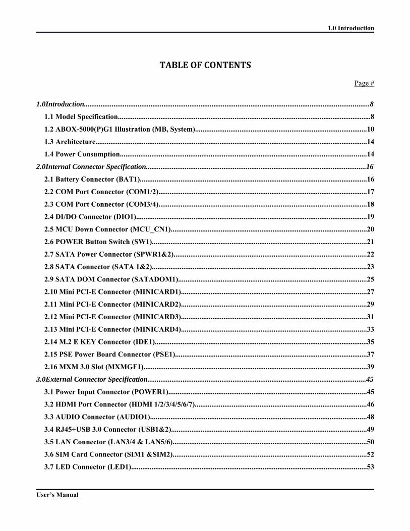
TABLEOFCONTENTS
Page #
1.0Introduction..........................................................................................................................................................8
1.1 Model Specification.........................................................................................................................................8
1.2 ABOX-5000(P)G1 Illustration (MB, System).............................................................................................10
1.3 Architecture...................................................................................................................................................14
1.4 Power Consumption.....................................................................................................................................14
2.0Internal Connector Specification.......................................................................................................................16
2.1 Battery Connector (BAT1)...........................................................................................................................16
2.2 COM Port Connector (COM1/2).................................................................................................................17
2.3 COM Port Connector (COM3/4).................................................................................................................18
2.4 DI/DO Connector (DIO1).............................................................................................................................19
2.5 MCU Down Connector (MCU_CN1)..........................................................................................................20
2.6 POWER Button Switch (SW1)....................................................................................................................21
2.7 SATA Power Connector (SPWR1&2)........................................................................................................22
2.8 SATA Connector (SATA 1&2)....................................................................................................................23
2.9 SATA DOM Connector (SATADOM1)......................................................................................................25
2.10 Mini PCI-E Connector (MINICARD1)....................................................................................................27
2.11 Mini PCI-E Connector (MINICARD2)....................................................................................................29
2.12 Mini PCI-E Connector (MINICARD3)....................................................................................................31
2.13 Mini PCI-E Connector (MINICARD4)....................................................................................................33
2.14 M.2 E KEY Connector (IDE1)...................................................................................................................35
2.15 PSE Power Board Connector (PSE1)........................................................................................................37
2.16 MXM 3.0 Slot (MXMGF1).........................................................................................................................39
3.0External Connector Specification......................................................................................................................45
3.1 Power Input Connector (POWER1)...........................................................................................................45
3.2 HDMI Port Connector (HDMI 1/2/3/4/5/6/7).............................................................................................46
3.3 AUDIO Connector (AUDIO1).....................................................................................................................48
3.4 RJ45+USB 3.0 Connector (USB1&2)..........................................................................................................49
3.5 LAN Connector (LAN3/4 & LAN5/6).........................................................................................................50
3.6 SIM Card Connector (SIM1 &SIM2).........................................................................................................52
3.7 LED Connector (LED1)...............................................................................................................................53
User’s Manual
1.0 Introduction
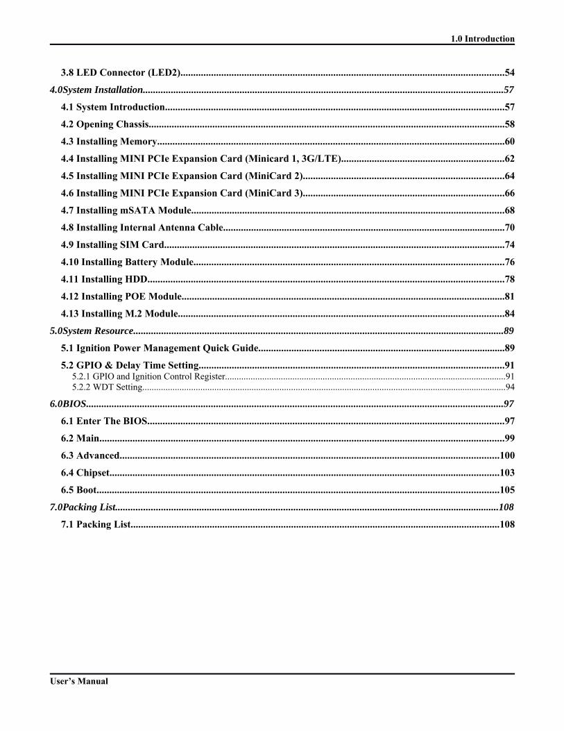
3.8 LED Connector (LED2)...............................................................................................................................54
4.0System Installation..............................................................................................................................................57
4.1 System Introduction.....................................................................................................................................57
4.2 Opening Chassis............................................................................................................................................58
4.3 Installing Memory.........................................................................................................................................60
4.4 Installing MINI PCIe Expansion Card (Minicard 1, 3G/LTE)................................................................62
4.5 Installing MINI PCIe Expansion Card (MiniCard 2)...............................................................................64
4.6 Installing MINI PCIe Expansion Card (MiniCard 3)...............................................................................66
4.7 Installing mSATA Module...........................................................................................................................68
4.8 Installing Internal Antenna Cable...............................................................................................................70
4.9 Installing SIM Card......................................................................................................................................74
4.10 Installing Battery Module..........................................................................................................................76
4.11 Installing HDD............................................................................................................................................78
4.12 Installing POE Module...............................................................................................................................81
4.13 Installing M.2 Module................................................................................................................................84
5.0System Resource..................................................................................................................................................89
5.1 Ignition Power Management Quick Guide.................................................................................................89
5.2 GPIO & Delay Time Setting........................................................................................................................915.2.1 GPIO and Ignition Control Register.........................................................................................................................915.2.2 WDT Setting.............................................................................................................................................................94
6.0BIOS....................................................................................................................................................................97
6.1 Enter The BIOS............................................................................................................................................97
6.2 Main...............................................................................................................................................................99
6.3 Advanced.....................................................................................................................................................100
6.4 Chipset.........................................................................................................................................................103
6.5 Boot..............................................................................................................................................................105
7.0Packing List.......................................................................................................................................................108
7.1 Packing List.................................................................................................................................................108
User’s Manual

1.0 Introduction
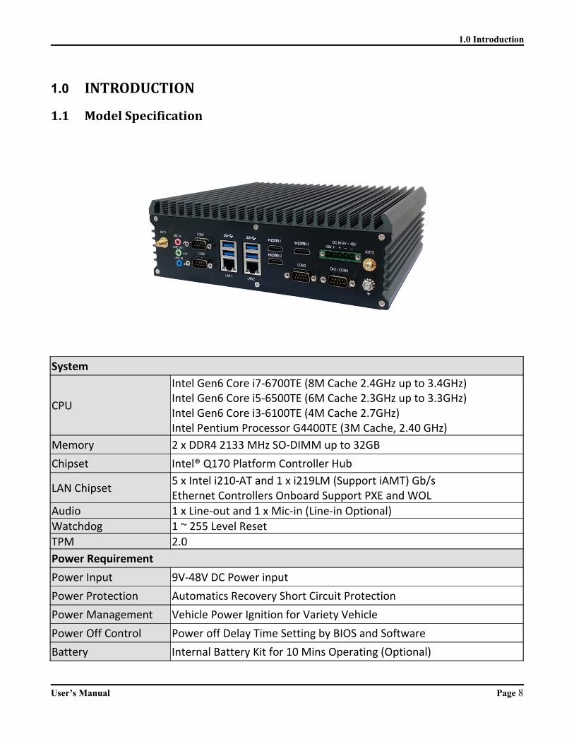
1.0INTRODUCTION
User’s Manual
1.0 Introduction
1.0 INTRODUCTION
1.1 ModelSpecification
System
CPU
Intel Gen6 Core i7‐6700TE (8M Cache 2.4GHz up to 3.4GHz)Intel Gen6 Core i5‐6500TE (6M Cache 2.3GHz up to 3.3GHz)Intel Gen6 Core i3‐6100TE (4M Cache 2.7GHz)Intel Pentium Processor G4400TE (3M Cache, 2.40 GHz)
Memory 2 x DDR4 2133 MHz SO‐DIMM up to 32GB
Chipset Intel® Q170 Platform Controller Hub
LAN Chipset5 x Intel i210‐AT and 1 x i219LM (Support iAMT) Gb/sEthernet Controllers Onboard Support PXE and WOL
Audio 1 x Line‐out and 1 x Mic‐in (Line‐in Optional)
Watchdog 1 ~ 255 Level Reset
TPM 2.0
Power Requirement
Power Input 9V‐48V DC Power input
Power Protection Automatics Recovery Short Circuit Protection
Power Management Vehicle Power Ignition for Variety Vehicle
Power Off Control Power off Delay Time Setting by BIOS and Software
Battery Internal Battery Kit for 10 Mins Operating (Optional)
User’s Manual Page 8
1.0 Introduction
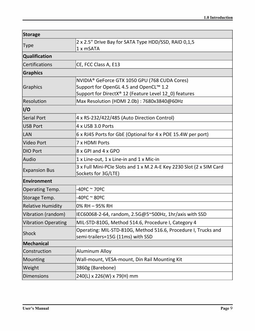
Storage
Type2 x 2.5" Drive Bay for SATA Type HDD/SSD, RAID 0,1,51 x mSATA
Qualification
Certifications CE, FCC Class A, E13
Graphics
GraphicsNVIDIA® GeForce GTX 1050 GPU (768 CUDA Cores)Support for OpenGL 4.5 and OpenCL™ 1.2Support for DirectX® 12 (Feature Level 12_0) features
Resolution Max Resolution (HDMI 2.0b) : 7680x3840@60Hz
I/O
Serial Port 4 x RS‐232/422/485 (Auto Direction Control)
USB Port 4 x USB 3.0 Ports
LAN 6 x RJ45 Ports for GbE (Optional for 4 x POE 15.4W per port)
Video Port 7 x HDMI Ports
DIO Port 8 x GPI and 4 x GPO
Audio 1 x Line‐out, 1 x Line‐in and 1 x Mic‐in
Expansion Bus3 x Full Mini‐PCIe Slots and 1 x M.2 A‐E Key 2230 Slot (2 x SIM Card Sockets for 3G/LTE)
Environment
Operating Temp. ‐40ºC ~ 70ºC
Storage Temp. ‐40ºC ~ 80ºC
Relative Humidity 0% RH – 95% RH
Vibration (random) IEC60068‐2‐64, random, 2.5G@5~500Hz, 1hr/axis with SSD
Vibration Operating MIL‐STD‐810G, Method 514.6, Procedure I, Category 4
ShockOperating: MIL‐STD‐810G, Method 516.6, Procedure I, Trucks and semi‐trailers=15G (11ms) with SSD
Mechanical
Construction Aluminum Alloy
Mounting Wall‐mount, VESA‐mount, Din Rail Mounting Kit
Weight 3860g (Barebone)
Dimensions 240(L) x 226(W) x 79(H) mm
User’s Manual Page 9

1.0 Introduction
1.2 FleetPC‐9Illustration(MB,System)
Main Board
User’s Manual Page 10

1.0 Introduction
User’s Manual Page 11
1.0 Introduction
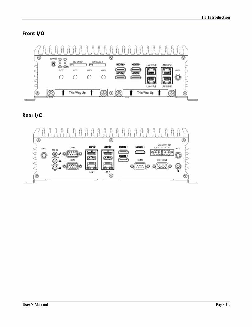
Front I/O
Rear I/O
User’s Manual Page 12

1.0 Introduction
System
User’s Manual Page 13
1.0 Introduction
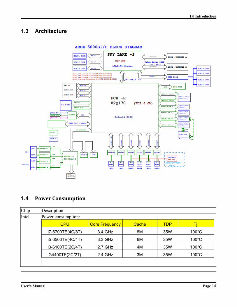
1.3 Architecture
1.4 PowerConsumption
Chip DescriptionIntel Power consumption:
CPU Core Frequency Cache TDP Tj
i7-6700TE(4C/8T) 3.4 GHz 8M 35W 100°C
i5-6500TE(4C/4T) 3.3 GHz 6M 35W 100°C
i3-6100TE(2C/4T) 2.7 GHz 4M 35W 100°C
G4400TE(2C/2T) 2.4 GHz 3M 35W 100°C
User’s Manual Page 14

2.0 Internal Connector Specification
2.0INTERNALCONNECTOR
SPECIFICATION
User’s Manual
2.0 Internal Connector Specification
2.0 INTERNALCONNECTORSPECIFICATION
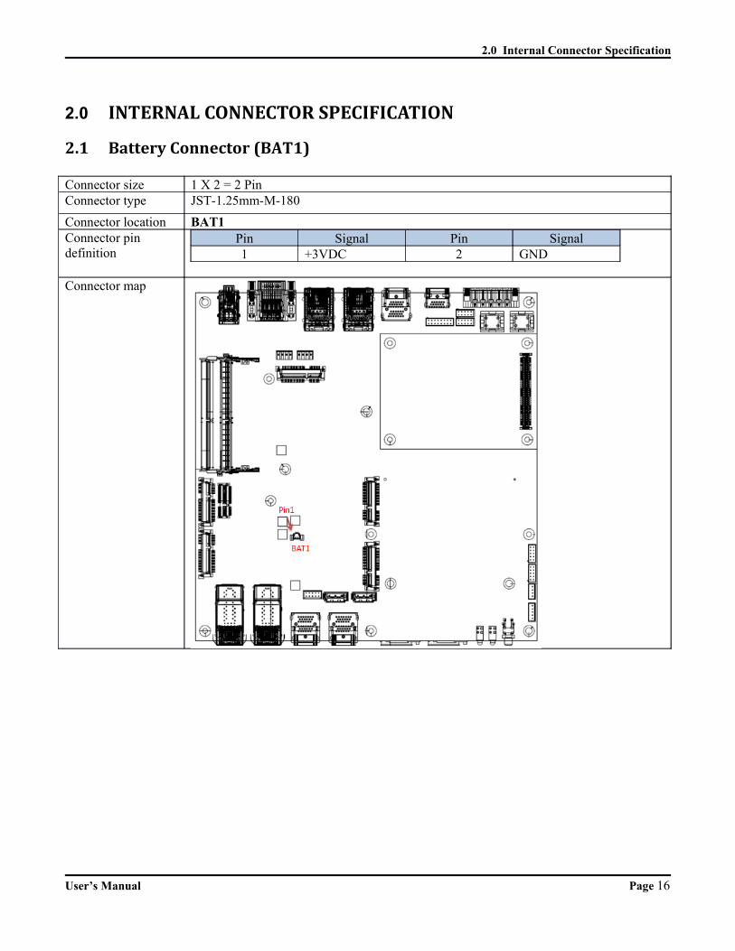
2.1 BatteryConnector(BAT1)
Connector size 1 X 2 = 2 PinConnector type JST-1.25mm-M-180
Connector location BAT1Connector pin definition
Pin Signal Pin Signal1 +3VDC 2 GND
Connector map
User’s Manual Page 16
2.0 Internal Connector Specification
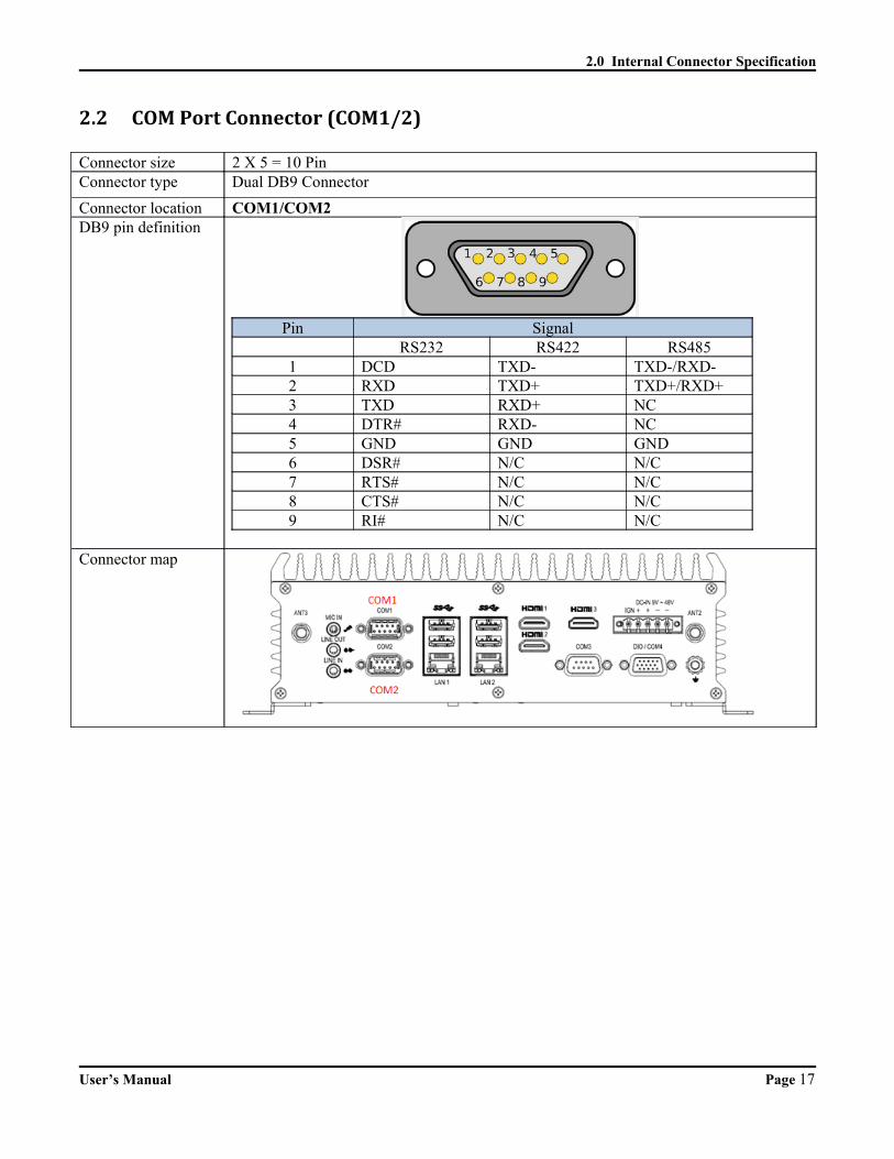
2.2 COMPortConnector(COM1/2)
Connector size 2 X 5 = 10 PinConnector type Dual DB9 Connector
Connector location COM1/COM2 DB9 pin definition
Pin SignalRS232 RS422 RS485
1 DCD TXD- TXD-/RXD-2 RXD TXD+ TXD+/RXD+3 TXD RXD+ NC4 DTR# RXD- NC5 GND GND GND6 DSR# N/C N/C7 RTS# N/C N/C8 CTS# N/C N/C9 RI# N/C N/C
Connector map
User’s Manual Page 17

2.0 Internal Connector Specification
2.3 COMPortConnector(COM3/4)
Connector size 2 X 5 = 10 PinConnector type JST-2.0mm-M-180
Connector location COM3/4Connector pin definition
Pin Signal Pin Signal1 DCD 2 RXD3 TXD 4 DTR5 GND 6 DSR#7 RTS# 8 CTS#9 RI# 10 GND
DB9 pin definition
Pin SignalRS232 RS422 RS485
1 COM2_DCD TXD- TXD-/RXD-2 COM2_RXD TXD+ TXD+/RXD+3 COM2_TXD RXD+ NC4 COM2_DTR RXD- NC5 GND GND GND6 DSR# N/C N/C7 RTS# N/C N/C8 CTS# N/C N/C9 RI# N/C N/C
User’s Manual Page 18

2.0 Internal Connector Specification
Connector map
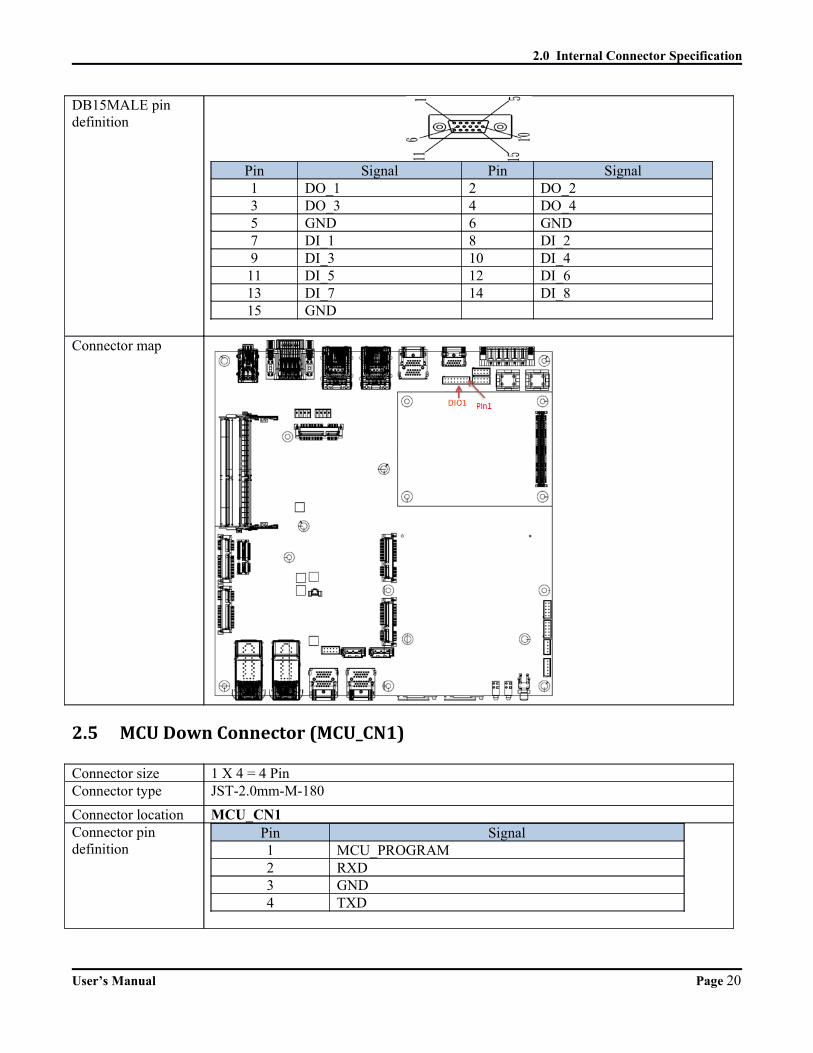
2.4 DI/DOConnector(DIO1)
Connector size 2 X 8 = 16 PinConnector type JST-2.0mm-M-180
Connector location DIO1Connector pin definition
Pin Signal Pin Signal1 DO_1 2 DO_23 DO_3 4 DO_45 GND 6 GND7 DI_1 8 DI_29 DI_3 10 DI_4
11 DI_5 12 DI_613 DI_7 14 DI_815 GND 16 CASE_GND
User’s Manual Page 19
2.0 Internal Connector Specification
DB15MALE pin definition
Pin Signal Pin Signal1 DO_1 2 DO_23 DO_3 4 DO_45 GND 6 GND7 DI_1 8 DI_29 DI_3 10 DI_4
11 DI_5 12 DI_613 DI_7 14 DI_815 GND
Connector map
2.5 MCUDownConnector(MCU_CN1)
Connector size 1 X 4 = 4 PinConnector type JST-2.0mm-M-180
Connector location MCU_CN1Connector pin definition
Pin Signal1 MCU_PROGRAM2 RXD3 GND4 TXD
User’s Manual Page 20

2.0 Internal Connector Specification
Connector map
2.6 POWERButtonSwitch(SW1)
Connector size 8 PINConnector type DIP-Switch
Connector location SW1Connector pin definition
Pin Signal1 GND2 PWRBTN#3 PWRBTN#
User’s Manual Page 21

2.0 Internal Connector Specification
4 GNDC1 PWRLED_P (RED LED)A1 PWRLED_N (GREEN LED)
MH1 N/CMH2 N/C
Connector map
2.7 SATAPowerConnector(SPWR1&2)
Connector size 1 X 4 = 4 PinConnector type WAFER 2.54mm-M-180
Connector location SPWR1 & 2
User’s Manual Page 22
2.0 Internal Connector Specification
Connector pin definition
Pin Signal1 +5V2 GND3 GND4 +12V
Connector map
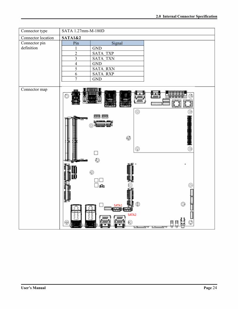
2.8 SATAConnector(SATA1&2)
Connector size 1 X 7 = 7 Pin
User’s Manual Page 23
2.0 Internal Connector Specification
Connector type SATA 1.27mm-M-180D
Connector location SATA1&2Connector pin definition
Pin Signal1 GND2 SATA_TXP3 SATA_TXN4 GND5 SATA_RXN6 SATA_RXP7 GND
Connector map
User’s Manual Page 24
2.0 Internal Connector Specification
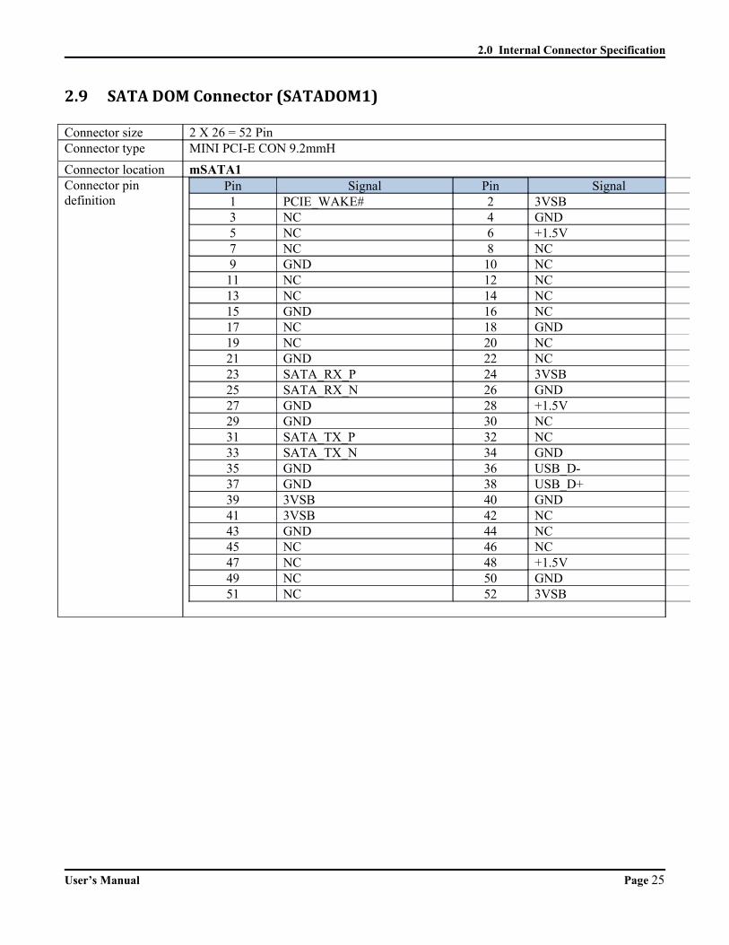
2.9 SATADOMConnector(SATADOM1)
Connector size 2 X 26 = 52 PinConnector type MINI PCI-E CON 9.2mmH
Connector location mSATA1Connector pin definition
Pin Signal Pin Signal1 PCIE_WAKE# 2 3VSB3 NC 4 GND5 NC 6 +1.5V7 NC 8 NC9 GND 10 NC
11 NC 12 NC13 NC 14 NC15 GND 16 NC17 NC 18 GND19 NC 20 NC21 GND 22 NC23 SATA_RX_P 24 3VSB25 SATA_RX_N 26 GND27 GND 28 +1.5V29 GND 30 NC31 SATA_TX_P 32 NC33 SATA_TX_N 34 GND35 GND 36 USB_D-37 GND 38 USB_D+39 3VSB 40 GND41 3VSB 42 NC43 GND 44 NC45 NC 46 NC47 NC 48 +1.5V49 NC 50 GND51 NC 52 3VSB
User’s Manual Page 25

2.0 Internal Connector Specification
Connector map
User’s Manual Page 26

2.0 Internal Connector Specification
2.10 MiniPCI‐EConnector(MINICARD1)
Connector size 2 X 26 = 52 PinConnector type MINI PCI-E CON 9.2mmH
Connector location MINICARD1 (3G/LTE)Connector pin definition
Pin Signal Pin Signal1 PCIE_WAKE# 2 3VSB3 NC 4 GND5 NC 6 NC7 NC 8 UIM1_PWR9 GND 10 UIM1_DATA
11 NC 12 UIM1_CLK13 NC 14 UIM1_RST15 GND 16 NC17 NC 18 GND19 NC 20 W_DISABLE#21 GND 22 PERST#23 NC 24 3VSB25 NC 26 GND27 GND 28 NC29 GND 30 NC31 NC 32 NC33 NC 34 GND35 GND 36 USB_D-37 GND 38 USB_D+39 3VSB 40 GND41 3VSB 42 LED_WWAN#43 GND 44 NC45 NC 46 NC47 NC 48 NC49 NC 50 GND51 NC 52 3VSB
User’s Manual Page 27

2.0 Internal Connector Specification
Connector map
User’s Manual Page 28
2.0 Internal Connector Specification
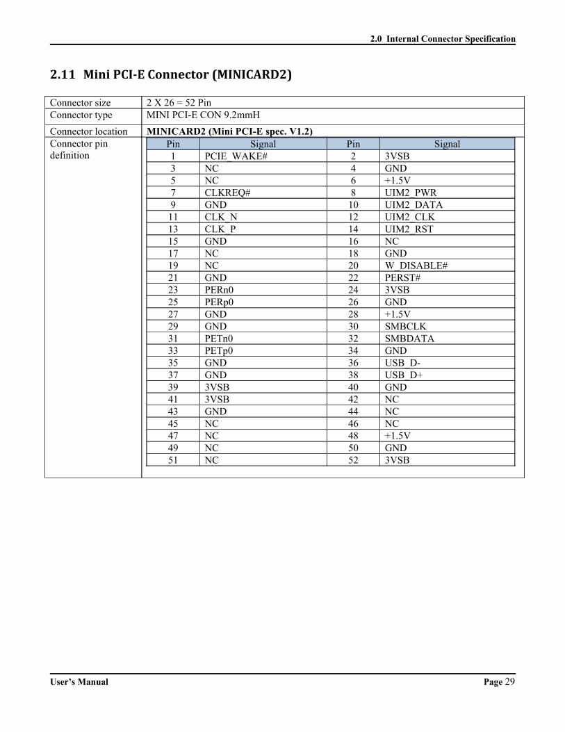
2.11 MiniPCI‐EConnector(MINICARD2)
Connector size 2 X 26 = 52 PinConnector type MINI PCI-E CON 9.2mmH
Connector location MINICARD2 (Mini PCI-E spec. V1.2)Connector pin definition
Pin Signal Pin Signal1 PCIE_WAKE# 2 3VSB3 NC 4 GND5 NC 6 +1.5V7 CLKREQ# 8 UIM2_PWR9 GND 10 UIM2_DATA
11 CLK_N 12 UIM2_CLK13 CLK_P 14 UIM2_RST15 GND 16 NC17 NC 18 GND19 NC 20 W_DISABLE#21 GND 22 PERST#23 PERn0 24 3VSB25 PERp0 26 GND27 GND 28 +1.5V29 GND 30 SMBCLK31 PETn0 32 SMBDATA33 PETp0 34 GND35 GND 36 USB_D-37 GND 38 USB_D+39 3VSB 40 GND41 3VSB 42 NC43 GND 44 NC45 NC 46 NC47 NC 48 +1.5V49 NC 50 GND51 NC 52 3VSB
User’s Manual Page 29
2.0 Internal Connector Specification
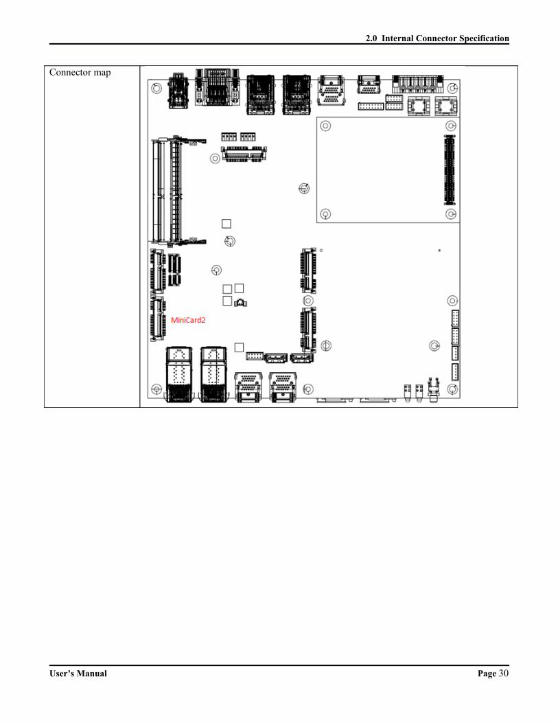
Connector map
User’s Manual Page 30
2.0 Internal Connector Specification
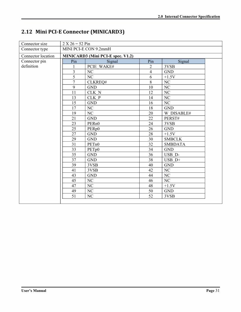
2.12 MiniPCI‐EConnector(MINICARD3)
Connector size 2 X 26 = 52 PinConnector type MINI PCI-E CON 9.2mmH
Connector location MINICARD3 (Mini PCI-E spec. V1.2)Connector pin definition
Pin Signal Pin Signal1 PCIE_WAKE# 2 3VSB3 NC 4 GND5 NC 6 +1.5V7 CLKREQ# 8 NC9 GND 10 NC
11 CLK_N 12 NC13 CLK_P 14 NC15 GND 16 NC17 NC 18 GND19 NC 20 W_DISABLE#21 GND 22 PERST#23 PERn0 24 3VSB25 PERp0 26 GND27 GND 28 +1.5V29 GND 30 SMBCLK31 PETn0 32 SMBDATA33 PETp0 34 GND35 GND 36 USB_D-37 GND 38 USB_D+39 3VSB 40 GND41 3VSB 42 NC43 GND 44 NC45 NC 46 NC47 NC 48 +1.5V49 NC 50 GND51 NC 52 3VSB
User’s Manual Page 31

2.0 Internal Connector Specification
Connector map
User’s Manual Page 32

2.0 Internal Connector Specification
2.13 MiniPCI‐EConnector(MINICARD4)
Connector size 2 X 26 = 52 PinConnector type MINI PCI-E CON 9.2mmH (Half Size OPT.)
Connector location MINICARD4 (Mini PCI-E spec. V1.2)Connector pin definition
Pin Signal Pin Signal1 PCIE_WAKE# 2 3VSB3 NC 4 GND5 NC 6 +1.5V7 CLKREQ# 8 NC9 GND 10 NC11 CLK_N 12 NC13 CLK_P 14 NC15 GND 16 NC17 NC 18 GND19 NC 20 W_DISABLE#21 GND 22 PERST#23 PERn0 24 3VSB25 PERp0 26 GND27 GND 28 +1.5V29 GND 30 SMBCLK31 PETn0 32 SMBDATA33 PETp0 34 GND35 GND 36 USB_D-37 GND 38 USB_D+39 3VSB 40 GND41 3VSB 42 NC43 GND 44 NC45 NC 46 NC47 NC 48 +1.5V49 NC 50 GND51 NC 52 3VSB
User’s Manual Page 33
2.0 Internal Connector Specification
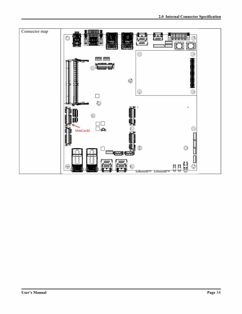
Connector map
User’s Manual Page 34
2.0 Internal Connector Specification
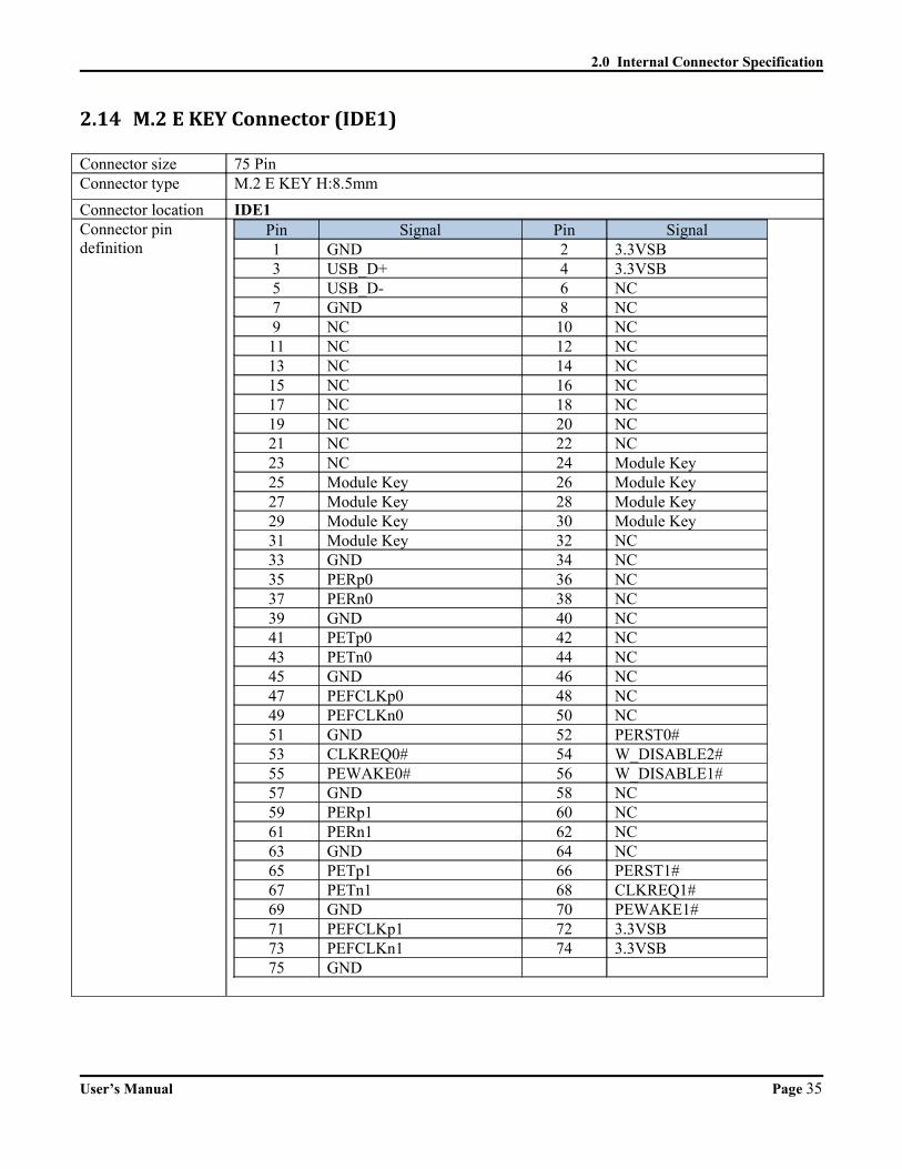
2.14 M.2EKEYConnector(IDE1)
Connector size 75 PinConnector type M.2 E KEY H:8.5mm
Connector location IDE1Connector pin definition
Pin Signal Pin Signal1 GND 2 3.3VSB3 USB_D+ 4 3.3VSB5 USB_D- 6 NC7 GND 8 NC9 NC 10 NC11 NC 12 NC13 NC 14 NC15 NC 16 NC17 NC 18 NC19 NC 20 NC21 NC 22 NC23 NC 24 Module Key25 Module Key 26 Module Key27 Module Key 28 Module Key29 Module Key 30 Module Key31 Module Key 32 NC33 GND 34 NC35 PERp0 36 NC37 PERn0 38 NC39 GND 40 NC41 PETp0 42 NC43 PETn0 44 NC45 GND 46 NC47 PEFCLKp0 48 NC49 PEFCLKn0 50 NC51 GND 52 PERST0#53 CLKREQ0# 54 W_DISABLE2#55 PEWAKE0# 56 W_DISABLE1#57 GND 58 NC59 PERp1 60 NC61 PERn1 62 NC63 GND 64 NC65 PETp1 66 PERST1#67 PETn1 68 CLKREQ1#69 GND 70 PEWAKE1#71 PEFCLKp1 72 3.3VSB73 PEFCLKn1 74 3.3VSB75 GND
User’s Manual Page 35

2.0 Internal Connector Specification
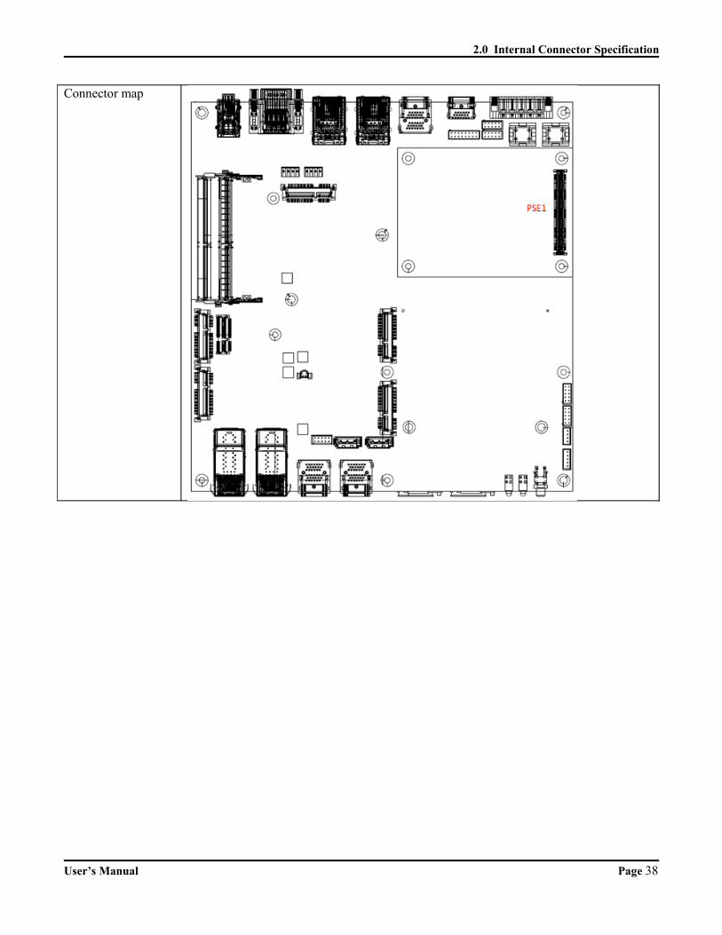
Connector map
User’s Manual Page 36
2.0 Internal Connector Specification
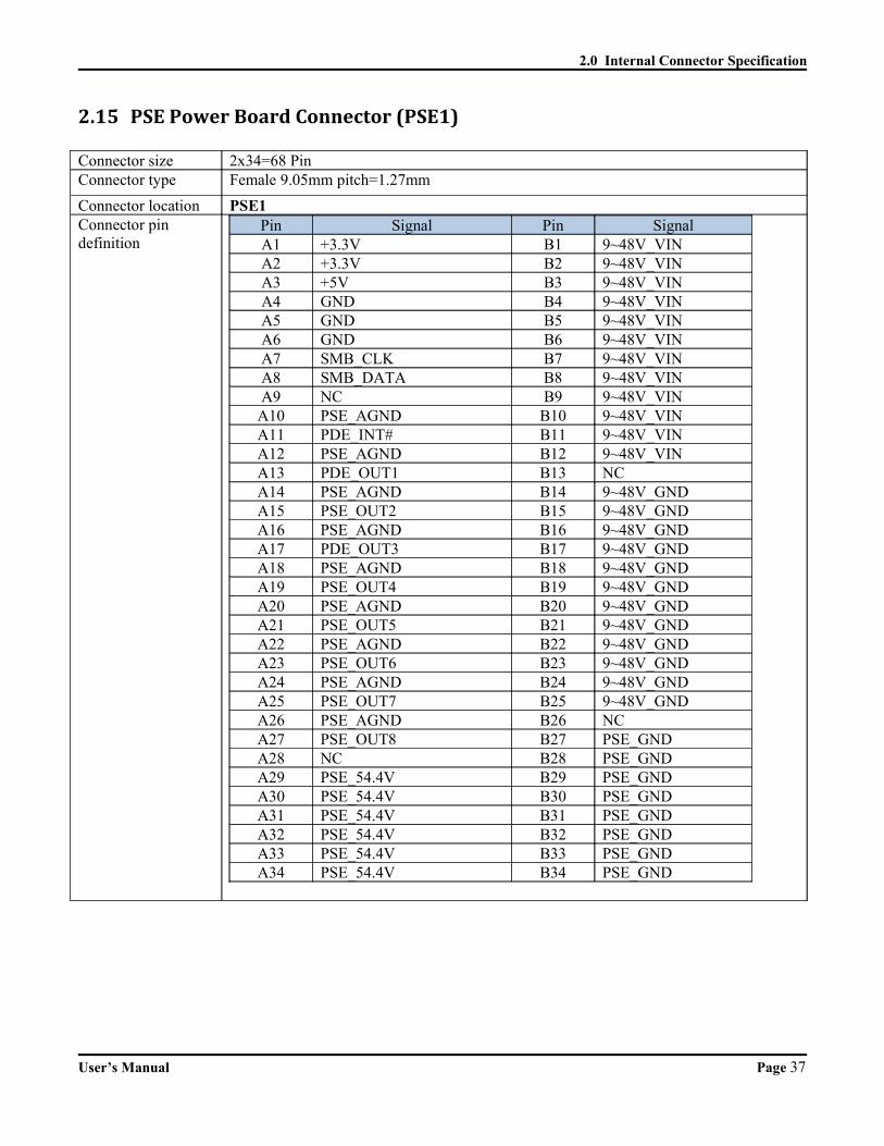
2.15 PSEPowerBoardConnector(PSE1)
Connector size 2x34=68 PinConnector type Female 9.05mm pitch=1.27mm
Connector location PSE1Connector pin definition
Pin Signal Pin SignalA1 +3.3V B1 9~48V_VINA2 +3.3V B2 9~48V_VINA3 +5V B3 9~48V_VINA4 GND B4 9~48V_VINA5 GND B5 9~48V_VINA6 GND B6 9~48V_VINA7 SMB_CLK B7 9~48V_VINA8 SMB_DATA B8 9~48V_VINA9 NC B9 9~48V_VIN
A10 PSE_AGND B10 9~48V_VINA11 PDE_INT# B11 9~48V_VINA12 PSE_AGND B12 9~48V_VINA13 PDE_OUT1 B13 NCA14 PSE_AGND B14 9~48V_GNDA15 PSE_OUT2 B15 9~48V_GNDA16 PSE_AGND B16 9~48V_GNDA17 PDE_OUT3 B17 9~48V_GNDA18 PSE_AGND B18 9~48V_GNDA19 PSE_OUT4 B19 9~48V_GNDA20 PSE_AGND B20 9~48V_GNDA21 PSE_OUT5 B21 9~48V_GNDA22 PSE_AGND B22 9~48V_GNDA23 PSE_OUT6 B23 9~48V_GNDA24 PSE_AGND B24 9~48V_GNDA25 PSE_OUT7 B25 9~48V_GNDA26 PSE_AGND B26 NCA27 PSE_OUT8 B27 PSE_GNDA28 NC B28 PSE_GNDA29 PSE_54.4V B29 PSE_GNDA30 PSE_54.4V B30 PSE_GNDA31 PSE_54.4V B31 PSE_GNDA32 PSE_54.4V B32 PSE_GNDA33 PSE_54.4V B33 PSE_GNDA34 PSE_54.4V B34 PSE_GND
User’s Manual Page 37
2.0 Internal Connector Specification
Connector map
User’s Manual Page 38
2.0 Internal Connector Specification
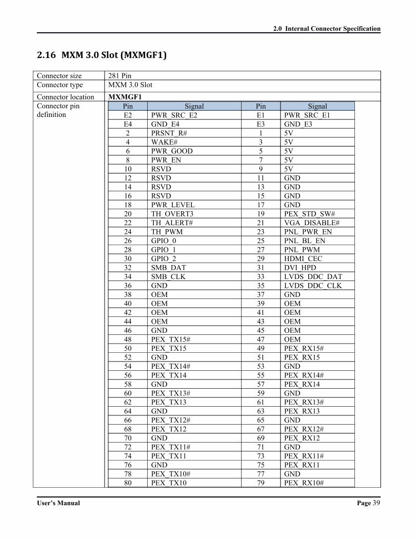
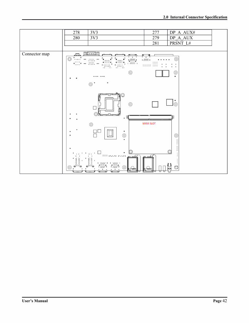
2.16 MXM3.0Slot(MXMGF1)
Connector size 281 PinConnector type MXM 3.0 Slot
Connector location MXMGF1Connector pin definition
Pin Signal Pin SignalE2 PWR_SRC_E2 E1 PWR_SRC_E1E4 GND_E4 E3 GND_E32 PRSNT_R# 1 5V4 WAKE# 3 5V6 PWR_GOOD 5 5V8 PWR_EN 7 5V10 RSVD 9 5V12 RSVD 11 GND14 RSVD 13 GND16 RSVD 15 GND18 PWR_LEVEL 17 GND20 TH_OVERT3 19 PEX_STD_SW#22 TH_ALERT# 21 VGA_DISABLE#24 TH_PWM 23 PNL_PWR_EN26 GPIO_0 25 PNL_BL_EN28 GPIO_1 27 PNL_PWM30 GPIO_2 29 HDMI_CEC32 SMB_DAT 31 DVI_HPD34 SMB_CLK 33 LVDS_DDC_DAT36 GND 35 LVDS_DDC_CLK38 OEM 37 GND40 OEM 39 OEM42 OEM 41 OEM44 OEM 43 OEM46 GND 45 OEM48 PEX_TX15# 47 OEM50 PEX_TX15 49 PEX_RX15#52 GND 51 PEX_RX1554 PEX_TX14# 53 GND56 PEX_TX14 55 PEX_RX14#58 GND 57 PEX_RX1460 PEX_TX13# 59 GND62 PEX_TX13 61 PEX_RX13#64 GND 63 PEX_RX1366 PEX_TX12# 65 GND68 PEX_TX12 67 PEX_RX12#70 GND 69 PEX_RX1272 PEX_TX11# 71 GND74 PEX_TX11 73 PEX_RX11#76 GND 75 PEX_RX1178 PEX_TX10# 77 GND80 PEX_TX10 79 PEX_RX10#
User’s Manual Page 39

2.0 Internal Connector Specification
82 GND 81 PEX_RX1084 PEX_TX9# 83 GND86 PEX_TX9 85 PEX_RX9#88 GND 87 PEX_RX990 PEX_TX8# 89 GND92 PEX_TX8 91 PEX_RX8#94 GND 93 PEX_RX896 PEX_TX7# 95 GND98 PEX_TX7 97 PEX_RX7#
100 GND 99 PEX_RX7102 PEX_TX6# 101 GND104 PEX_TX6 103 PEX_RX6#106 GND 105 PEX_RX6108 PEX_TX5# 107 GND110 PEX_TX5 109 PEX_RX5#112 GND 111 PEX_RX5114 PEX_TX4# 113 GND116 PEX_TX4 115 PEX_RX4#118 GND 117 PEX_RX4120 PEX_TX3# 119 GND122 PEX_TX3 121 PEX_RX3#124 GND 123 PEX_RX3126 KEY 125 GND128 KEY 127 KEY130 KEY 129 KEY132 KEY 131 KEY134 GND 133 GND136 PEX_TX2# 135 PEX_RX2#138 PEX_TX2 137 PEX_RX2140 GND 139 GND142 PEX_TX1# 141 PEX_RX1#144 PEX_TX1 143 PEX_RX1146 GND 145 GND148 PEX_TX0# 147 PEX_RX0#150 PEX_TX0 149 PEX_RX0152 GND 151 GND154 CLK_REQ# 153 PEX_REFCLK#156 PEX_RST# 155 PEX_REFCLK158 VGA_DDC_DAT 157 GND160 VGA_DDC_CLK 159 RSVD162 VGA_VSYC 161 RSVD164 VGA_HSYC 163 RSVD166 GND 165 RSVD168 VGA_RED 167 RSVD170 VGA_GREEN 169 LVDS_UCLK#172 VGA_BLUE 171 LVDS_UCLK174 GND 173 GND176 LVDS_LCLK# 175 LVDS_UTX3#178 LVDS_LCLK 177 LVDS_UTX3
User’s Manual Page 40
2.0 Internal Connector Specification
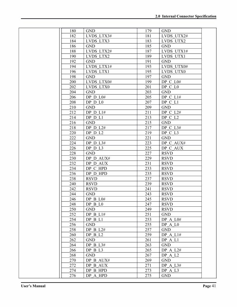
180 GND 179 GND182 LVDS_LTX3# 181 LVDS_UTX2#184 LVDS_LTX3 183 LVDS_UTX2186 GND 185 GND188 LVDS_LTX2# 187 LVDS_UTX1#190 LVDS_LTX2 189 LVDS_UTX1192 GND 191 GND194 LVDS_LTX1# 193 LVDS_UTX0#196 LVDS_LTX1 195 LVDS_UTX0198 GND 197 GND200 LVDS_LTX0# 199 DP_C_L0#202 LVDS_LTX0 201 DP_C_L0204 GND 203 GND206 DP_D_L0# 205 DP_C_L1#208 DP_D_L0 207 DP_C_L1210 GND 209 GND212 DP_D_L1# 211 DP_C_L2#214 DP_D_L1 213 DP_C_L2216 GND 215 GND218 DP_D_L2# 217 DP_C_L3#220 DP_D_L2 219 DP_C_L3222 GND 221 GND224 DP_D_L3# 223 DP_C_AUX#226 DP_D_L3 225 DP_C_AUX228 GND 227 RSVD230 DP_D_AUX# 229 RSVD232 DP_D_AUX 231 RSVD234 DP_C_HPD 233 RSVD236 DP_D_HPD 235 RSVD238 RSVD 237 RSVD240 RSVD 239 RSVD242 RSVD 241 RSVD244 GND 243 RSVD246 DP_B_L0# 245 RSVD248 DP_B_L0 247 RSVD250 GND 249 RSVD252 DP_B_L1# 251 GND254 DP_B_L1 253 DP_A_L0#256 GND 255 DP_A_L0258 DP_B_L2# 257 GND260 DP_B_L2 259 DP_A_L1#262 GND 261 DP_A_L1264 DP_B_L3# 263 GND266 DP_B_L3 265 DP_A_L2#268 GND 267 DP_A_L2270 DP_B_AUX# 269 GND272 DP_B_AUX 271 DP_A_L3#274 DP_B_HPD 273 DP_A_L3276 DP_A_HPD 275 GND
User’s Manual Page 41
2.0 Internal Connector Specification
278 3V3 277 DP_A_AUX#280 3V3 279 DP_A_AUX
281 PRSNT_L#
Connector map
User’s Manual Page 42

2.0 Internal Connector Specification
User’s Manual Page 43
3.0 External Connector Specification
3.0EXTERNALCONNECTOR
SPECIFICATION
User’s Manual
3.0 External Connector Specification
3.0 EXTERNALCONNECTORSPECIFICATION
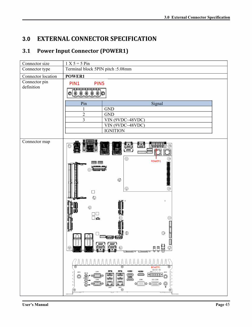
3.1 PowerInputConnector(POWER1)
Connector size 1 X 5 = 5 PinConnector type Terminal block 5PIN pitch :5.08mm
Connector location POWER1Connector pin definition
Pin Signal1 GND2 GND3 VIN (9VDC~48VDC)
VIN (9VDC~48VDC)IGNITION
Connector map
User’s Manual Page 45
3.0 External Connector Specification
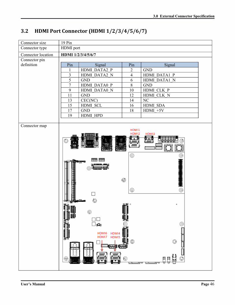
3.2 HDMIPortConnector(HDMI1/2/3/4/5/6/7)
Connector size 19 PinConnector type HDMI port
Connector location HDMI 1/2/3/4/5/6/7Connector pin definition Pin Signal Pin Signal
1 HDMI_DATA2_P 2 GND3 HDMI_DATA2_N 4 HDMI_DATA1_P5 GND 6 HDMI_DATA1_N7 HDMI_DATA0_P 8 GND9 HDMI_DATA0_N 10 HDMI_CLK_P
11 GND 12 HDMI_CLK_N13 CEC(NC) 14 NC15 HDMI_SCL 16 HDMI_SDA17 GND 18 HDMI_+5V19 HDMI_HPD
Connector map
User’s Manual Page 46
3.0 External Connector Specification
User’s Manual Page 47
3.0 External Connector Specification
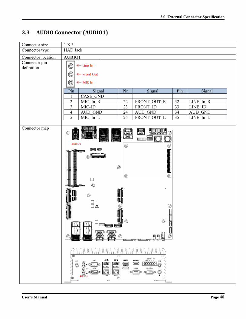
3.3 AUDIOConnector(AUDIO1)
Connector size 1 X 3Connector type HAD Jack
Connector location AUDIO1Connector pin definition
Pin Signal Pin Signal Pin Signal1 CASE_GND2 MIC_In_R 22 FRONT_OUT_R 32 LINE_In_R3 MIC-JD 23 FRONT_JD 33 LINE_JD4 AUD_GND 24 AUD_GND 34 AUD_GND5 MIC_In_L 25 FRONT_OUT_L 35 LINE_In_L
Connector map
User’s Manual Page 48
3.0 External Connector Specification
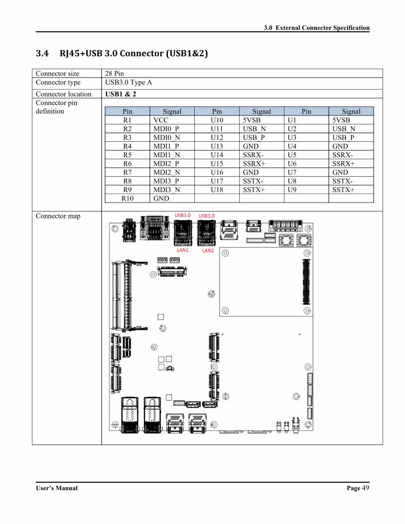
3.4 RJ45+USB3.0Connector(USB1&2)
Connector size 28 PinConnector type USB3.0 Type A
Connector location USB1 & 2Connector pin definition Pin Signal Pin Signal Pin Signal
R1 VCC U10 5VSB U1 5VSBR2 MDI0_P U11 USB_N U2 USB_NR3 MDI0_N U12 USB_P U3 USB_PR4 MDI1_P U13 GND U4 GNDR5 MDI1_N U14 SSRX- U5 SSRX-R6 MDI2_P U15 SSRX+ U6 SSRX+R7 MDI2_N U16 GND U7 GNDR8 MDI3_P U17 SSTX- U8 SSTX-R9 MDI3_N U18 SSTX+ U9 SSTX+
R10 GND
Connector map
User’s Manual Page 49
3.0 External Connector Specification
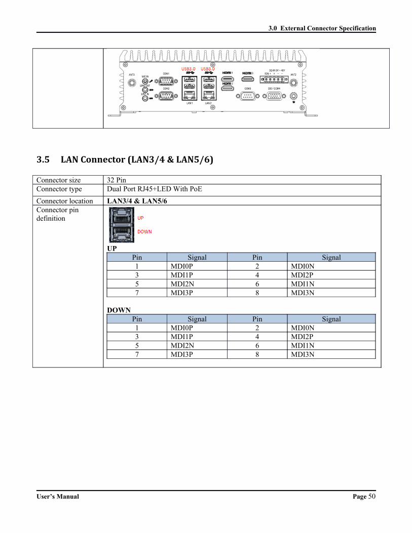
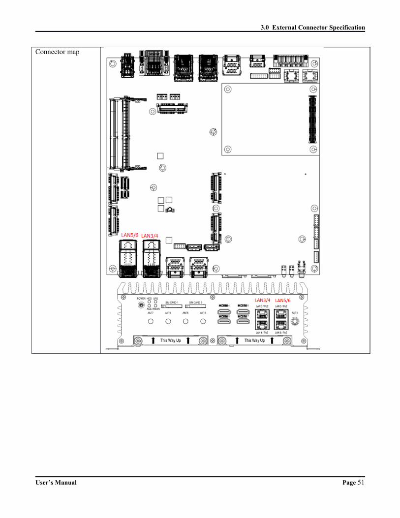
3.5 LANConnector(LAN3/4&LAN5/6)
Connector size 32 PinConnector type Dual Port RJ45+LED With PoE
Connector location LAN3/4 & LAN5/6Connector pin definition
UPPin Signal Pin Signal1 MDI0P 2 MDI0N3 MDI1P 4 MDI2P5 MDI2N 6 MDI1N7 MDI3P 8 MDI3N
DOWNPin Signal Pin Signal1 MDI0P 2 MDI0N3 MDI1P 4 MDI2P5 MDI2N 6 MDI1N7 MDI3P 8 MDI3N
User’s Manual Page 50
3.0 External Connector Specification
Connector map
User’s Manual Page 51
3.0 External Connector Specification
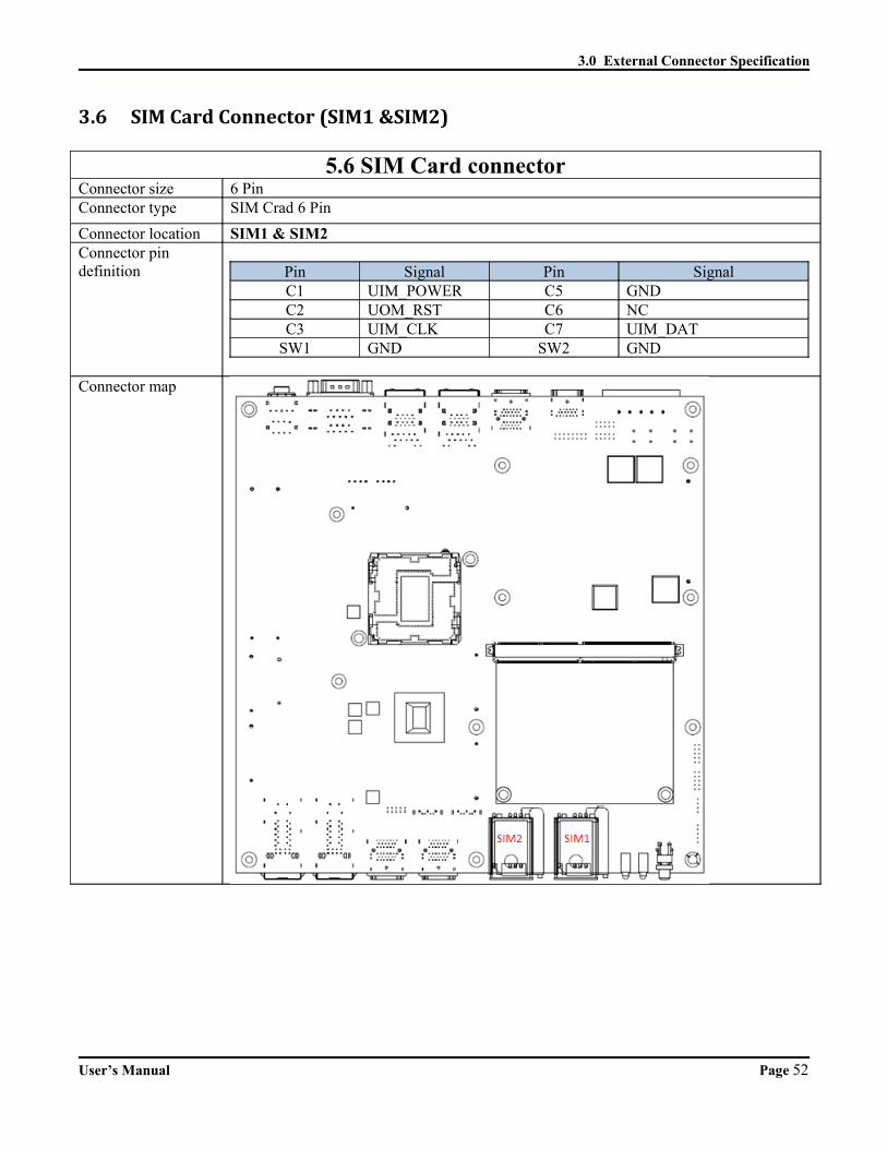
3.6 SIMCardConnector(SIM1&SIM2)
5.6 SIM Card connectorConnector size 6 PinConnector type SIM Crad 6 Pin
Connector location SIM1 & SIM2Connector pin definition Pin Signal Pin Signal
C1 UIM_POWER C5 GNDC2 UOM_RST C6 NCC3 UIM_CLK C7 UIM_DAT
SW1 GND SW2 GND
Connector map
User’s Manual Page 52
3.0 External Connector Specification
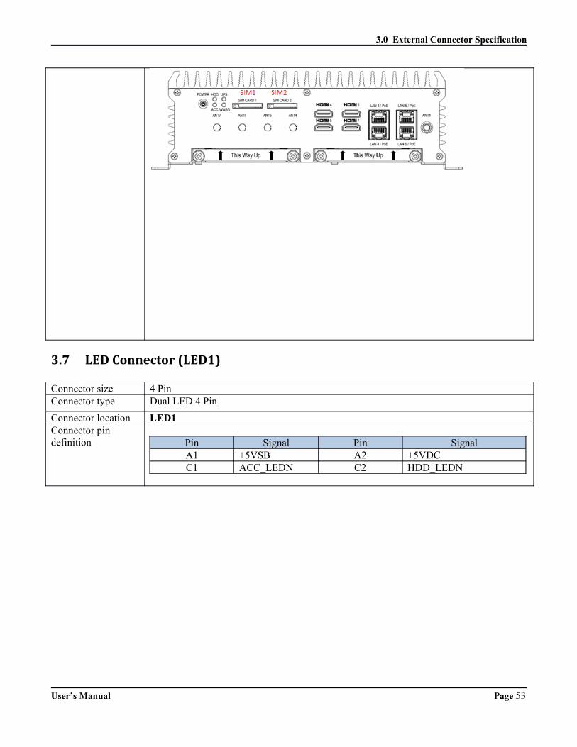
3.7 LEDConnector(LED1)
Connector size 4 PinConnector type Dual LED 4 Pin
Connector location LED1Connector pin definition Pin Signal Pin Signal
A1 +5VSB A2 +5VDCC1 ACC_LEDN C2 HDD_LEDN
User’s Manual Page 53

3.0 External Connector Specification
Connector map
3.8 LEDConnector(LED2)
Connector size 4 PinConnector type Dual LED 4 Pin
Connector location LED2Connector pin definition Pin Signal Pin Signal
A1 +5VSB A2 +5VDC
User’s Manual Page 54

3.0 External Connector Specification
C1 WWAN_LEDN C2 UPS_LEDN
Connector map
User’s Manual Page 55

4.0 System Installation
4.0SYSTEMINSTALLATION
User’s Manual

4.0 System Installation
4.0 SYSTEMINSTALLATION
4.1 SystemIntroduction
User’s Manual Page 57
4.0 System Installation
4.2 OpeningChassis
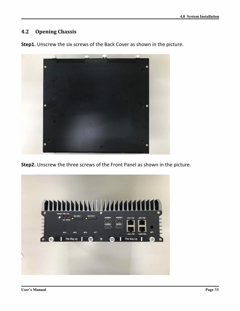
Step1. Unscrew the six screws of the Back Cover as shown in the picture.
Step2. Unscrew the three screws of the Front Panel as shown in the picture.
User’s Manual Page 58

4.0 System Installation
Step3. Unscrew the three screws of the Rear Panel as shown in the picture.
Step4. Open Bottom Cover as shown in the picture.
User’s Manual Page 59
4.0 System Installation
4.3 InstallingMemory
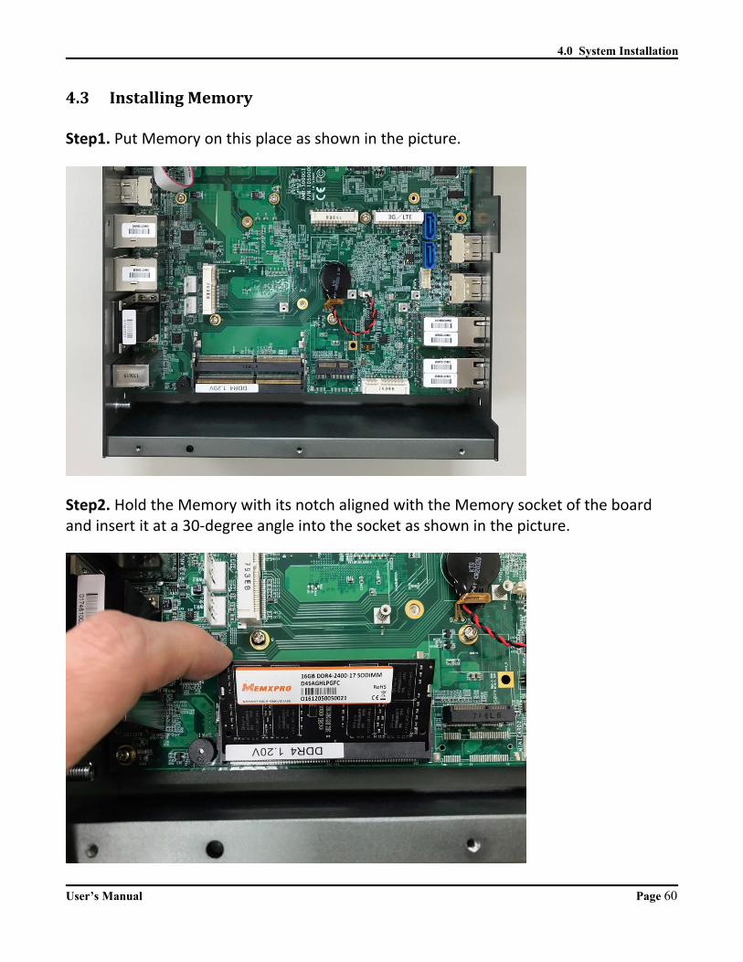
Step1. Put Memory on this place as shown in the picture.
Step2. Hold the Memory with its notch aligned with the Memory socket of the board and insert it at a 30‐degree angle into the socket as shown in the picture.
User’s Manual Page 60

4.0 System Installation
Step3. Press down on the Memory so that the tabs of the socket lock on both sides of the module as shown in the picture.
User’s Manual Page 61
4.0 System Installation
4.4 InstallingMINIPCIeExpansionCard(Minicard1,3G/LTE)
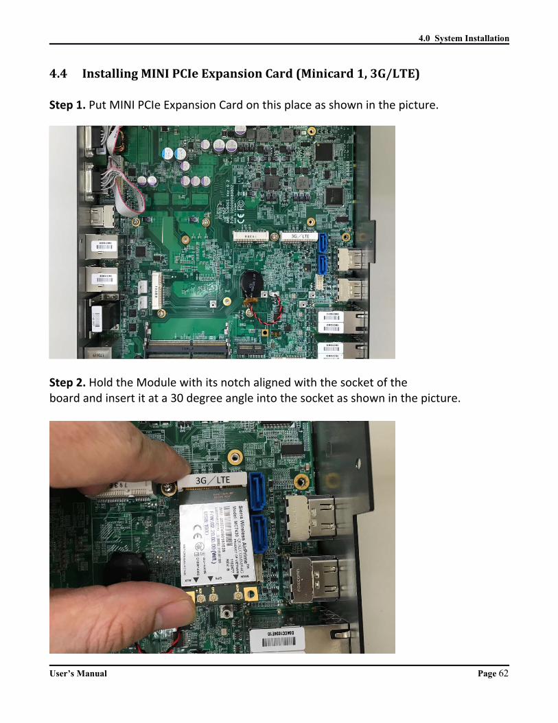
Step 1. Put MINI PCIe Expansion Card on this place as shown in the picture.
Step 2. Hold the Module with its notch aligned with the socket of theboard and insert it at a 30 degree angle into the socket as shown in the picture.
User’s Manual Page 62
4.0 System Installation
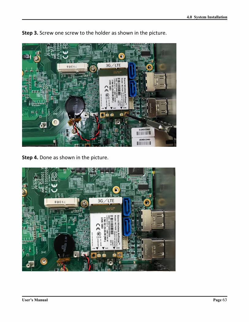
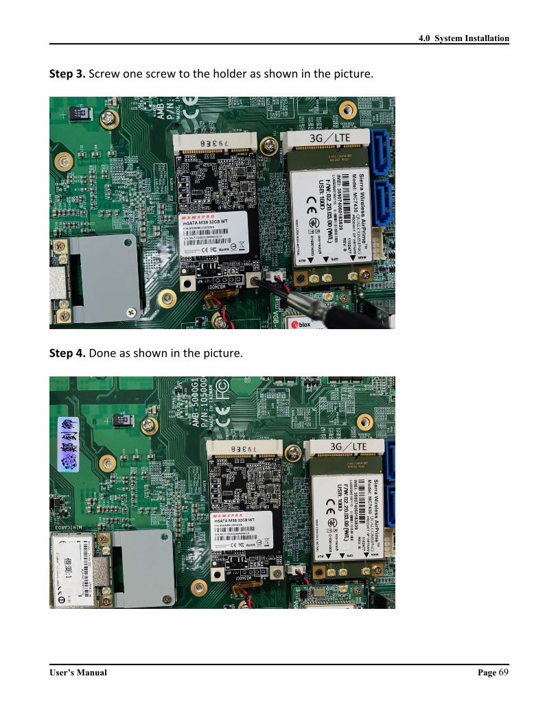
Step 3. Screw one screw to the holder as shown in the picture.
Step 4. Done as shown in the picture.
User’s Manual Page 63
4.0 System Installation
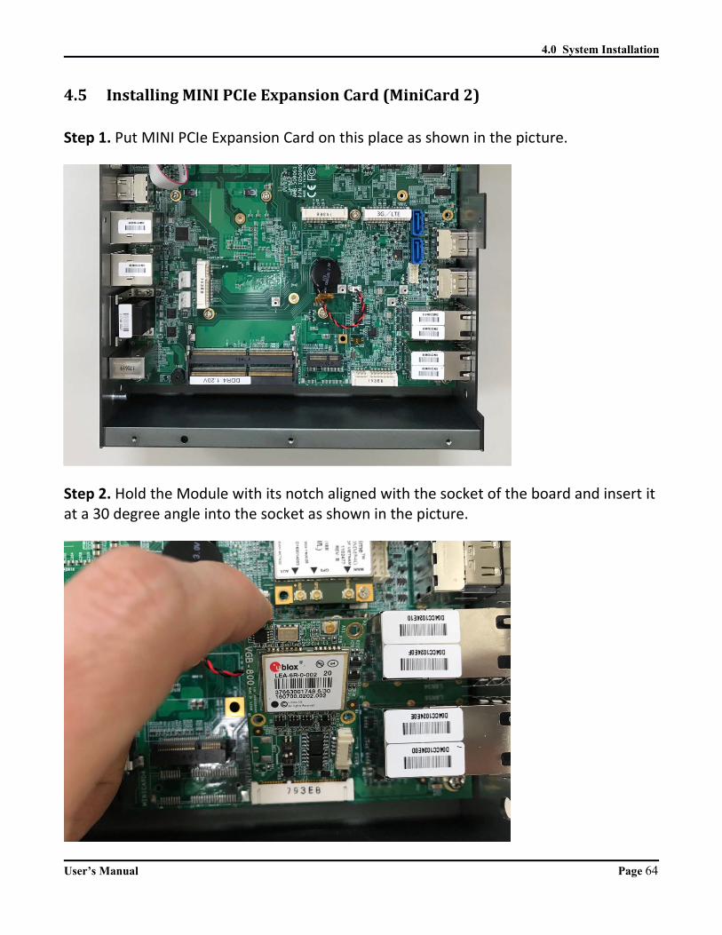
4.5 InstallingMINIPCIeExpansionCard(MiniCard2)
Step 1. Put MINI PCIe Expansion Card on this place as shown in the picture.
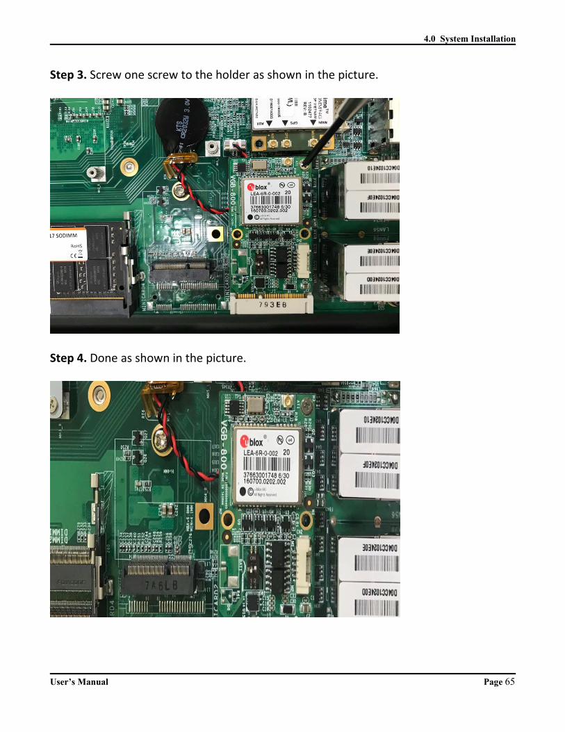
Step 2. Hold the Module with its notch aligned with the socket of the board and insert itat a 30 degree angle into the socket as shown in the picture.
User’s Manual Page 64
4.0 System Installation
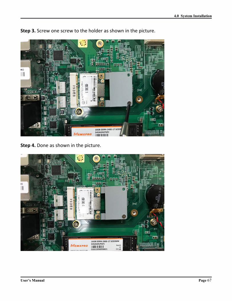
Step 3. Screw one screw to the holder as shown in the picture.
Step 4. Done as shown in the picture.
User’s Manual Page 65

4.0 System Installation
4.6 InstallingMINIPCIeExpansionCard(MiniCard3)
Step 1. Put MINI PCIe Expansion Card on this place as shown in the picture.
Step 2. Hold the Module with its notch aligned with the socket of the board and insert itat a 30 degree angle into the socket as shown in the picture.
User’s Manual Page 66
4.0 System Installation
Step 3. Screw one screw to the holder as shown in the picture.
Step 4. Done as shown in the picture.
User’s Manual Page 67
4.0 System Installation
4.7 InstallingmSATAModule
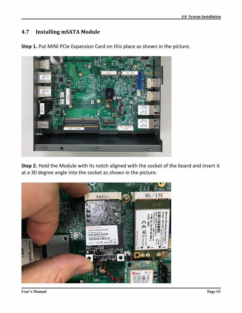
Step 1. Put MINI PCIe Expansion Card on this place as shown in the picture.
Step 2. Hold the Module with its notch aligned with the socket of the board and insert itat a 30 degree angle into the socket as shown in the picture.
User’s Manual Page 68
4.0 System Installation
Step 3. Screw one screw to the holder as shown in the picture.
Step 4. Done as shown in the picture.
User’s Manual Page 69

4.0 System Installation
4.8 InstallingInternalAntennaCable
Step 1. Take the SMA Connector and Plug into IO Panel as shown in the picture.
Step 2. Put the Washer into the SMA Connector as shown in the picture.
User’s Manual Page 70
4.0 System Installation
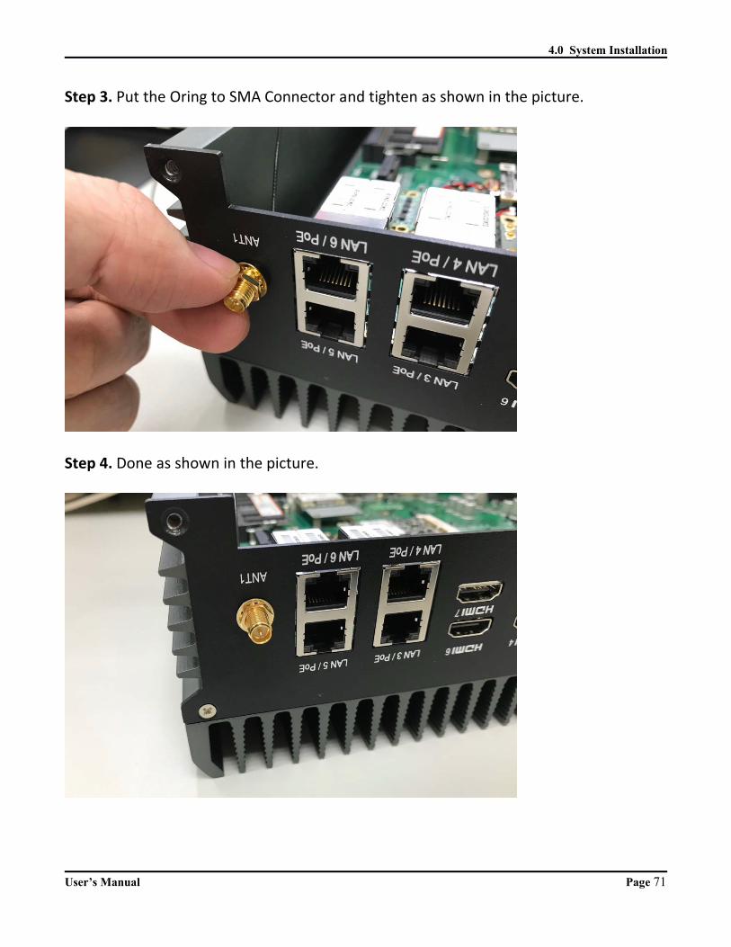
Step 3. Put the Oring to SMA Connector and tighten as shown in the picture.
Step 4. Done as shown in the picture.
User’s Manual Page 71
4.0 System Installation
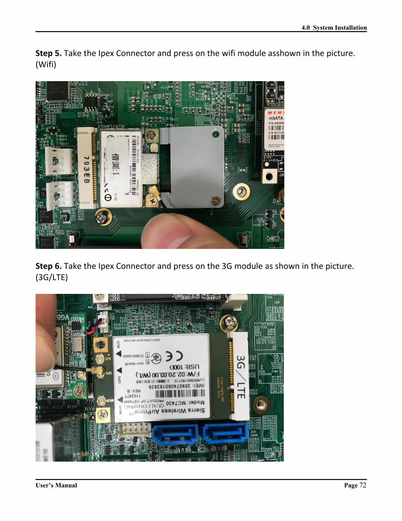
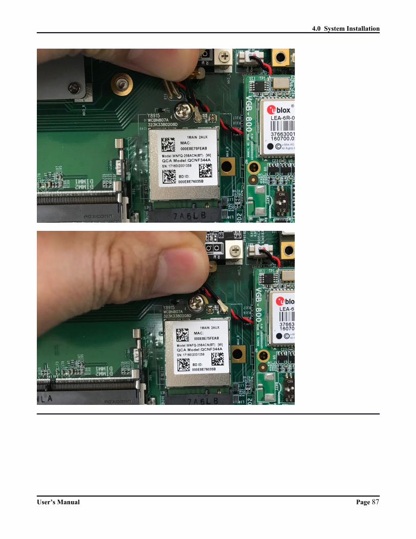
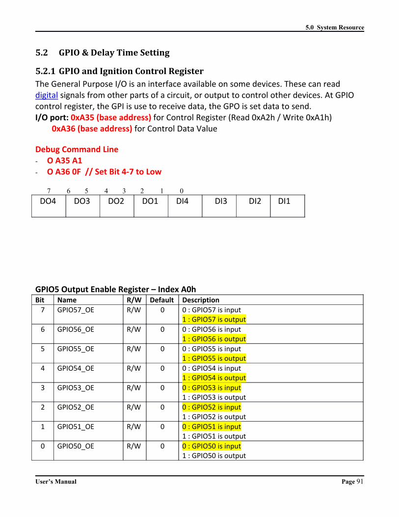
Step 5. Take the Ipex Connector and press on the wifi module asshown in the picture.(Wifi)
Step 6. Take the Ipex Connector and press on the 3G module as shown in the picture. (3G/LTE)
User’s Manual Page 72

4.0 System Installation
Step 7. Take the Ipex Connector and press on the GPS module as shown in the picture. (GPS)
User’s Manual Page 73
4.0 System Installation
4.9 InstallingSIMCard
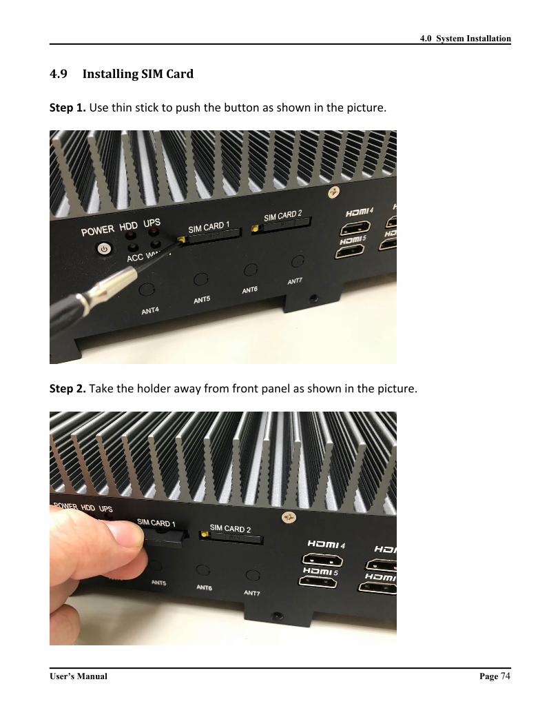
Step 1. Use thin stick to push the button as shown in the picture.
Step 2. Take the holder away from front panel as shown in the picture.
User’s Manual Page 74
4.0 System Installation
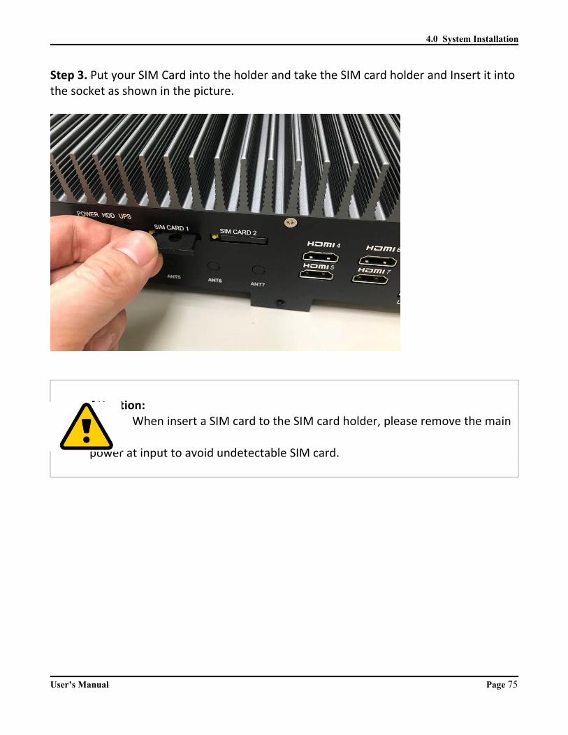
Step 3. Put your SIM Card into the holder and take the SIM card holder and Insert it into the socket as shown in the picture.
Attention:When insert a SIM card to the SIM card holder, please remove the main
power at input to avoid undetectable SIM card.
User’s Manual Page 75
4.0 System Installation
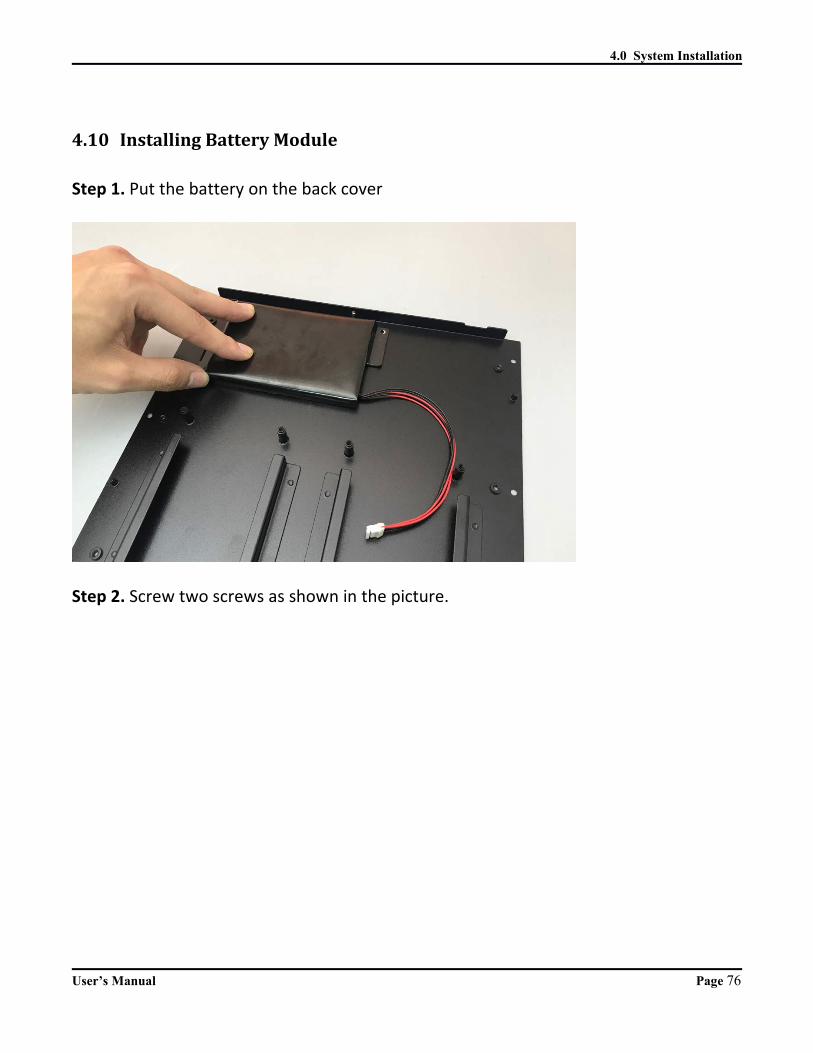
4.10 InstallingBatteryModule
Step 1. Put the battery on the back cover
Step 2. Screw two screws as shown in the picture.
User’s Manual Page 76
4.0 System Installation
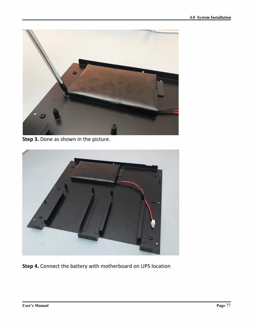
Step 3. Done as shown in the picture.
Step 4. Connect the battery with motherboard on UPS location
User’s Manual Page 77
4.0 System Installation
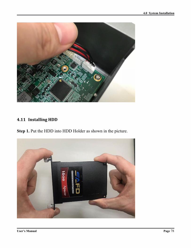
4.11 InstallingHDD
Step 1. Put the HDD into HDD Holder as shown in the picture.
User’s Manual Page 78
4.0 System Installation
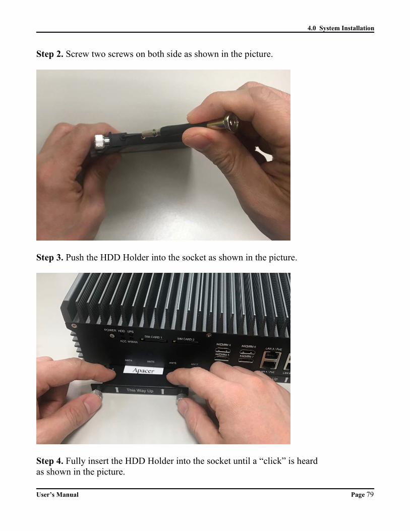
Step 2. Screw two screws on both side as shown in the picture.
Step 3. Push the HDD Holder into the socket as shown in the picture.
Step 4. Fully insert the HDD Holder into the socket until a “click” is heardas shown in the picture.
User’s Manual Page 79
4.0 System Installation
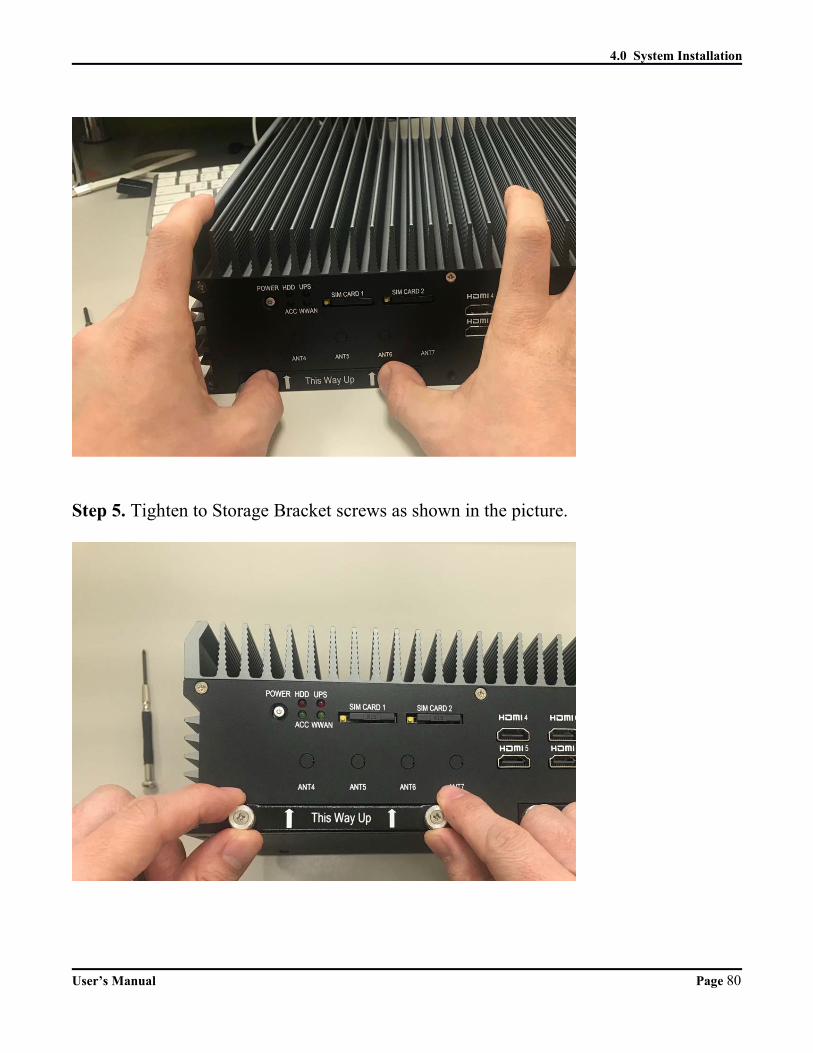
Step 5. Tighten to Storage Bracket screws as shown in the picture.
User’s Manual Page 80
4.0 System Installation
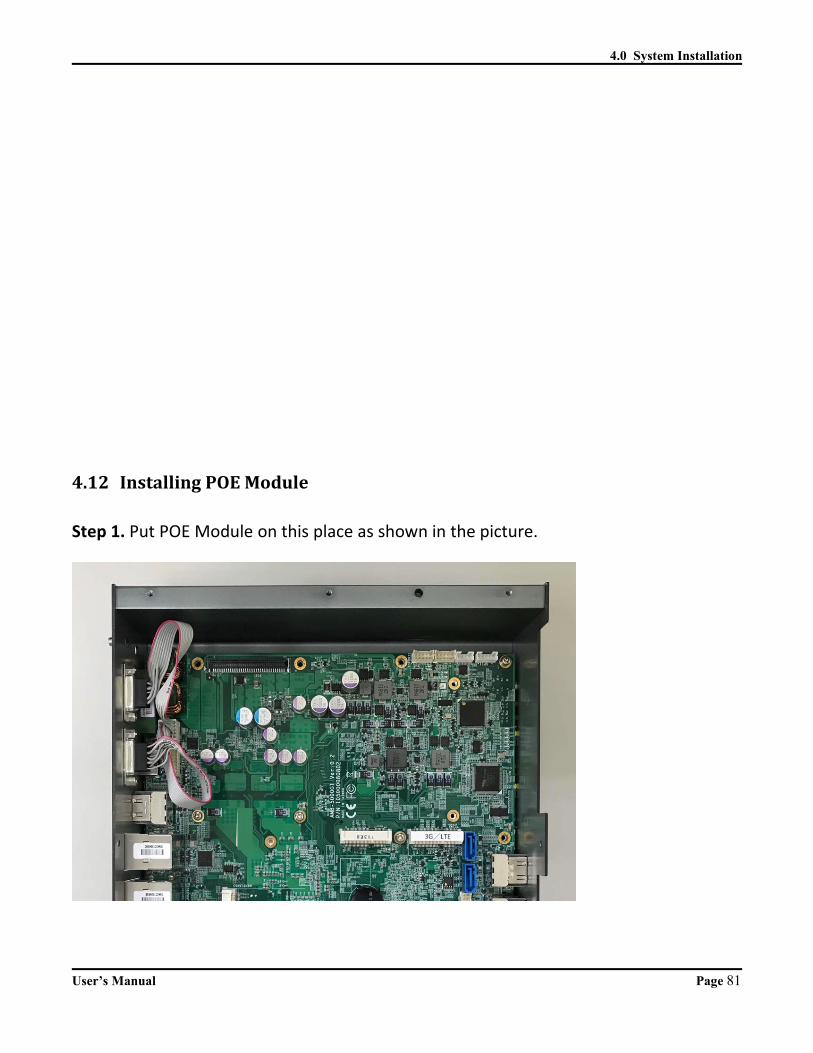
4.12 InstallingPOEModule
Step 1. Put POE Module on this place as shown in the picture.
User’s Manual Page 81
4.0 System Installation
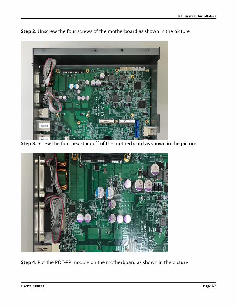
Step 2. Unscrew the four screws of the motherboard as shown in the picture
Step 3. Screw the four hex standoff of the motherboard as shown in the picture
Step 4. Put the POE‐8P module on the motherboard as shown in the picture
User’s Manual Page 82
4.0 System Installation
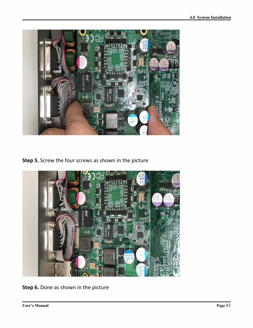
Step 5. Screw the four screws as shown in the picture
Step 6. Done as shown in the picture
User’s Manual Page 83
4.0 System Installation
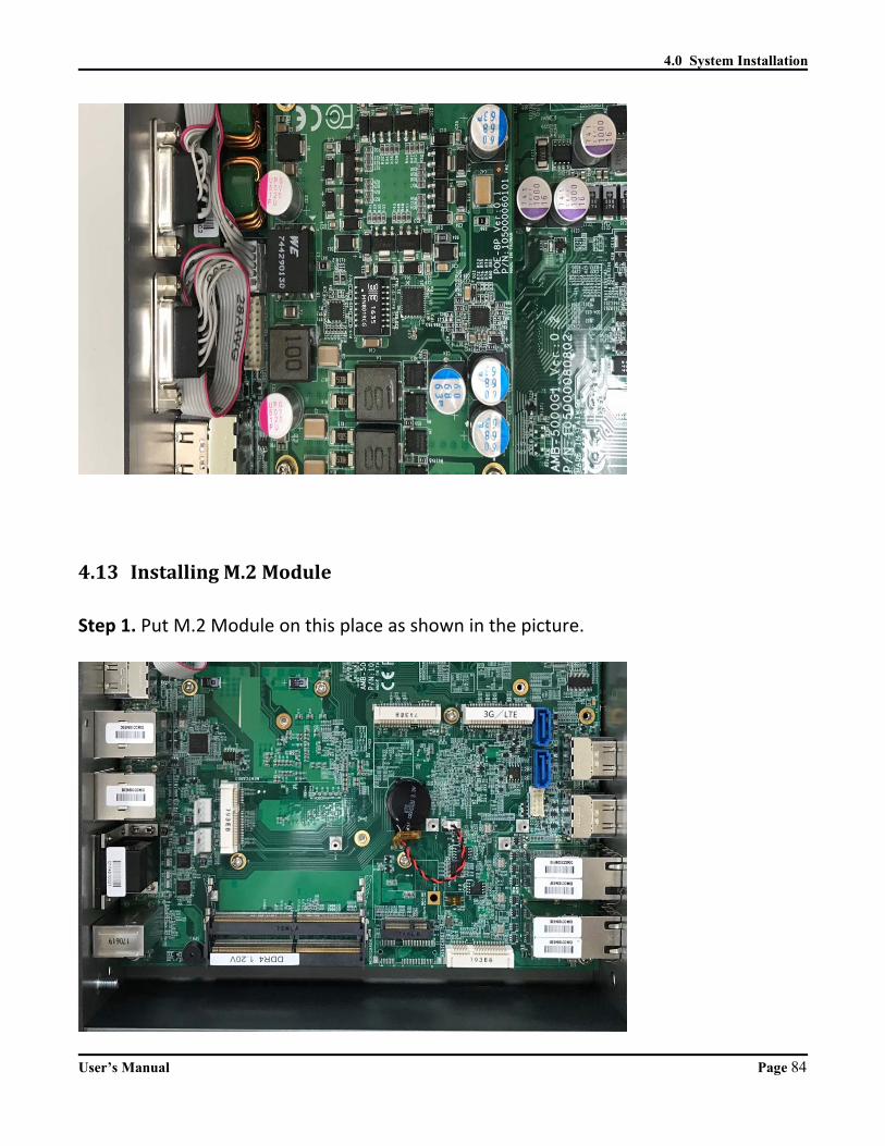
4.13 InstallingM.2Module
Step 1. Put M.2 Module on this place as shown in the picture.
User’s Manual Page 84
4.0 System Installation
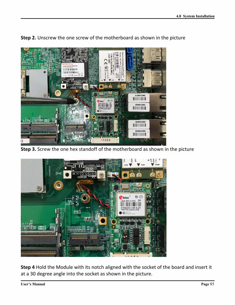
Step 2. Unscrew the one screw of the motherboard as shown in the picture
Step 3. Screw the one hex standoff of the motherboard as shown in the picture
Step 4 Hold the Module with its notch aligned with the socket of the board and insert it at a 30 degree angle into the socket as shown in the picture.
User’s Manual Page 85
4.0 System Installation
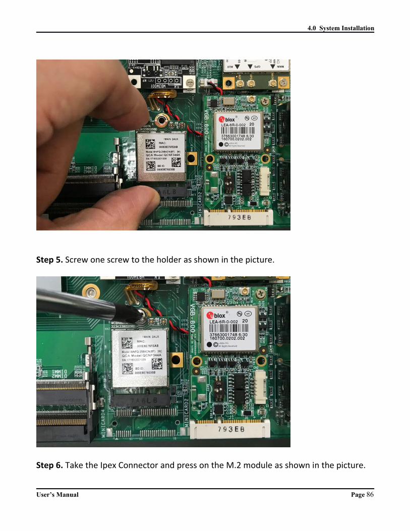
Step 5. Screw one screw to the holder as shown in the picture.
Step 6. Take the Ipex Connector and press on the M.2 module as shown in the picture.
User’s Manual Page 86
4.0 System Installation
User’s Manual Page 87

5.0 System Resource
5.0SYSTEMRESOURCE
User’s Manual

5.0 System Resource
5.0 SYSTEMRESOURCE
5.1 IgnitionPowerManagementQuickGuide
Startup/shutdown conditions from the IGNITION signal:
IGNITION startup signal must be valid during 3 sec. (anti noise protection).
IGNITION shutdown – IGNITION signal must be inactive during 3 Sec, then PIC controller initiate Power Button signal (OS must be set to shutdown from the Power Button). It generate Main Button shutdown event and then goes to complete power off.
Typically the system can start only from IGNITION signal, because startup PIC controller is disconnected from the power source.
The system can be switched off from:
Power IGNITION OFF signal.
ACPI OS shutdown
Power Button – generate ACPI event (OS dependent).
Power Ignition Startup Procedure
User’s Manual Page 89

5.0 System Resource
Power Ignition Shutdown Procedure
Power Management
Power‐off delay time is selectable by Software to disable and enable in 0‐99 minutes
Ignition On/Off status detectable by SW
If the ignition is off and the system is still on after 3 Sec, FleetPC‐9 will shut down automatically.
If the ignition is turned on again and the power‐off delay is in progress, FleetPC‐9 will cancel the delay function and will continue to operate normally.
If the ignition is turned on again and the power‐off delay ended, FleetPC‐9 will shut down completely will power‐on again automatically.
User’s Manual Page 90
5.0 System Resource
5.2 GPIO&DelayTimeSetting
5.2.1 GPIOandIgnitionControlRegisterThe General Purpose I/O is an interface available on some devices. These can read digital signals from other parts of a circuit, or output to control other devices. At GPIO control register, the GPI is use to receive data, the GPO is set data to send.I/O port: 0xA35 (base address) for Control Register (Read 0xA2h / Write 0xA1h) 0xA36 (base address) for Control Data Value
Debug Command Line- O A35 A1- O A36 0F // Set Bit 4‐7 to Low
7 6 5 4 3 2 1 0
DO4 DO3 DO2 DO1 DI4 DI3 DI2 DI1
GPIO5 Output Enable Register – Index A0hBit Name R/W Default Description
7 GPIO57_OE R/W 0 0 : GPIO57 is input1 : GPIO57 is output
6 GPIO56_OE R/W 0 0 : GPIO56 is input1 : GPIO56 is output
5 GPIO55_OE R/W 0 0 : GPIO55 is input1 : GPIO55 is output
4 GPIO54_OE R/W 0 0 : GPIO54 is input1 : GPIO54 is output
3 GPIO53_OE R/W 0 0 : GPIO53 is input1 : GPIO53 is output
2 GPIO52_OE R/W 0 0 : GPIO52 is input1 : GPIO52 is output
1 GPIO51_OE R/W 0 0 : GPIO51 is input1 : GPIO51 is output
0 GPIO50_OE R/W 0 0 : GPIO50 is input1 : GPIO50 is output
User’s Manual Page 91
5.0 System Resource
GPIO5 Output Data Register – Index A1h
Bit Name R/W Default Description
7 GPIO57_DATA R/W 1 GPIO57 output data in output mode.
6 GPIO56_DATA R/W 1 GPIO56 output data in output mode.
5 GPIO55_DATA R/W 1 GPIO55 output data in output mode.
4 GPIO54_DATA R/W 1 GPIO54 output data in output mode.
3 GPIO53_DATA R/W 1 GPIO53 output data in output mode.
2 GPIO52_DATA R/W 1 GPIO52 output data in output mode.
1 GPIO51_DATA R/W 1 GPIO51 output data in output mode.
0 GPIO50_DATA R/W 1 GPIO50 output data in output mode.
GPIO5 Pin Status Register – Index A2h
Bit Name R/W Default Description
7 GPIO57_ST R 1 GPIO57 pin status.
6 GPIO56_ST R 1 GPIO56 pin status.
5 GPIO55_ST R 1 GPIO55 pin status.
4 GPIO54_ST R 1 GPIO54 pin status.
3 GPIO53_ST R 1 GPIO53 pin status.
2 GPIO52_ST R 1 GPIO52 pin status.
1 GPIO51_ST R 1 GPIO51 pin status.
0 GPIO50_ST R 1 GPIO50 pin status.
User’s Manual Page 92
5.0 System Resource
GPIO5 Drive Enable Register – Index A3hBit Name R/W Default Description
7 GPIO57_DRV_ENST R/W 0 GPIO57 Drive Enable0 : GPIO57 is open drain.1 : GPIO57 is push pull.
6 GPIO56_DRV_ENST R/W 0 GPIO57 Drive Enable0 : GPIO56 is open drain.1 : GPIO56 is push pull.
5 GPIO55_DRV_ENST R/W 0 GPIO57 Drive Enable0 : GPIO55 is open drain.1 : GPIO55 is push pull.
4 GPIO54_DRV_ENST R/W 0 GPIO57 Drive Enable0 : GPIO54 is open drain.1 : GPIO54 is push pull.
3 GPIO53_DRV_ENST R/W 0 GPIO57 Drive Enable0 : GPIO53 is open drain.1 : GPIO53 is push pull.
2 GPIO52_DRV_ENST R/W 0 GPIO57 Drive Enable0 : GPIO52 is open drain.1 : GPIO52 is push pull.
1 GPIO51_DRV_ENST R/W 0 GPIO57 Drive Enable0 : GPIO51 is open drain.1 : GPIO51 is push pull.
0 GPIO50_DRV_ENST R/W 0 GPIO57 Drive Enable0 : GPIO50 is open drain.1 : GPIO50 is push pull.
I/O port: I/O port: 0xA35 (base address) for Control Register (Read 0xF2h bit 3) 0xA36 (base address) for Control Data Value
7 6 5 4 3 2 1 0
X X X X Ignition Status
X X X
Debug Command Line- O A35 F2- I A36 // Check Bit 3 Status
User’s Manual Page 93
5.0 System Resource
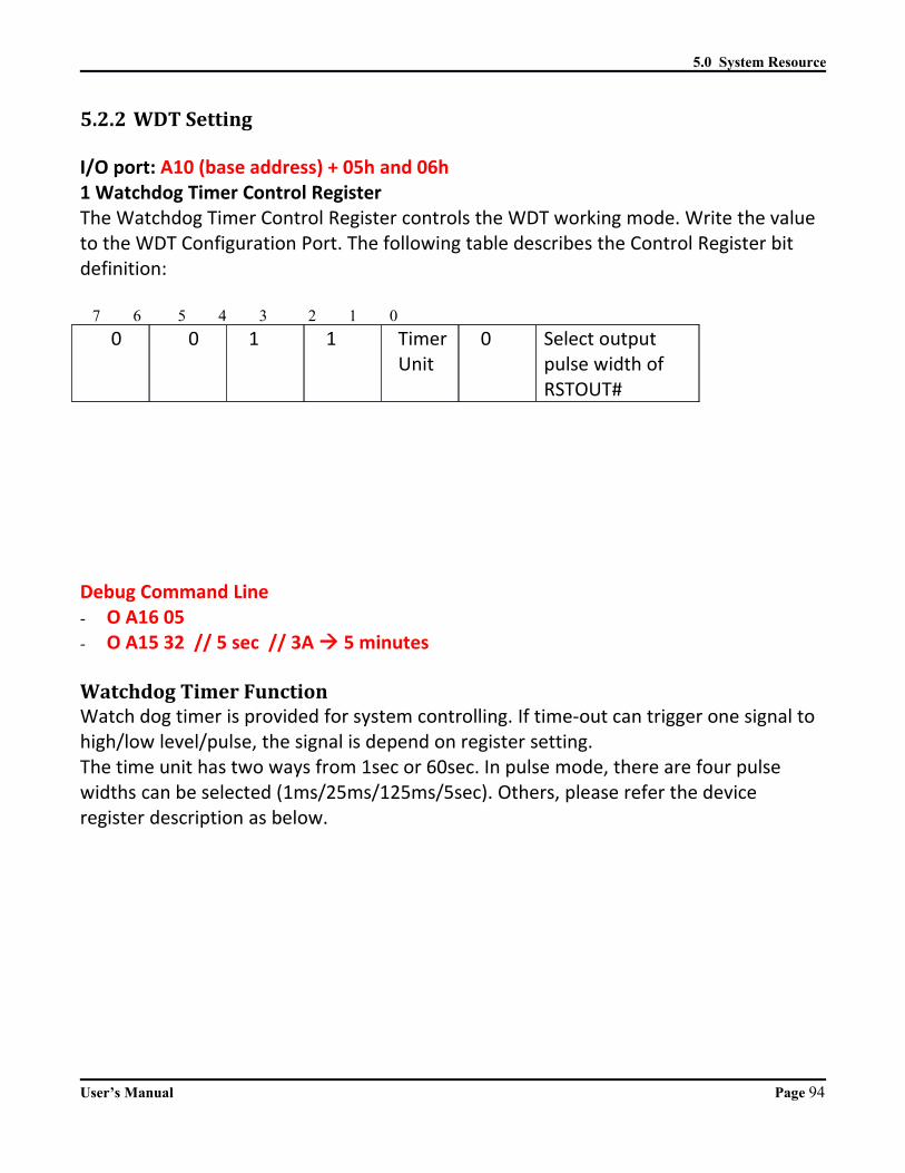
5.2.2 WDTSetting
I/O port: A10 (base address) + 05h and 06h1 Watchdog Timer Control RegisterThe Watchdog Timer Control Register controls the WDT working mode. Write the value to the WDT Configuration Port. The following table describes the Control Register bit definition:
7 6 5 4 3 2 1 0
0 0 1 1 TimerUnit
0 Select output pulse width of RSTOUT#
Debug Command Line- O A16 05- O A15 32 // 5 sec // 3A 5 minutes
WatchdogTimerFunctionWatch dog timer is provided for system controlling. If time‐out can trigger one signal to high/low level/pulse, the signal is depend on register setting.The time unit has two ways from 1sec or 60sec. In pulse mode, there are four pulse widths can be selected (1ms/25ms/125ms/5sec). Others, please refer the device register description as below.
User’s Manual Page 94

5.0 System Resource
Watchdog Timer Configuration Register 1‐ base address +05hBit Name R/W Default Description
7 Reserved R 0 Reserved
6 WDTMOUT_STS R/W 0 If watchdog timeout event occurs, this bit will be set to 1. Write a 1 to this bit will clear it to 0.
5 WD_EN R/W 0 If this bit is set to 1, the counting of watchdog time is enabled.
4 WD_PULSE R/W 0 Select output mode (0:level, 1:pulse) of RSTOUT# by setting this bit.
3 WD_UNIT R/W 0 Select time unit (0:1sec, 1:60sec) of watchdog timer by setting this bit.
2 WD_HACTIVE R/W 0 Select output polarity of RETOUT# (1:high active, 0:low active) by setting the bit.
1‐0 WD_PSWIDTH R/W 0 Select output pulse width of RSTOUT#0:1 ms 1:25 ms2:125 ms 3:5 sec
Watchdog Timer Configuration Register 2‐ base address +06hBit Name R/W Default Description
7‐0 WD_TIME R/W 0 Time of watchdog timer
Watchdog PME Control Register ‐ base address + 0AhBit Name R/W Default Description
7 WDT_PME R ‐‐ The PME StatusThis bit will set when WDT_PME_EN is set and the watchdog timer is 1 unit before time out (of time out)
6 WDT_PME_EN R/W 0 0 : Disable Watchdog PME.1 : Enable Watchdog PME
5‐1 Reserved ‐‐ ‐‐ Reserved
0 WDOUT_EN R/W 0 0 : disable Watchdog time out output via WDTRST#1 : enable Watchdog time out output via WDTRST#
User’s Manual Page 95

6.0 BIOS
6.0BIOS
User’s Manual

6.0 BIOS
6.0 BIOS
6.1 EnterTheBIOSPower on the computer and the system will start POST (Power On Self Test) process.When the message below appears on the screen, press (DEL) key to enter Setup.
PressDELtoenterSETUPIf the message disappears before you respond and you still wish to enter Setup, restartthe system by turning it OFF and On or pressing the RESET button. You may also restartthe system by simultaneously pressing <Ctrl>, <Alt>, and <Delete> keys.
Important The items under each BIOS category described in this chapter are under continuous
update for better system performance. Therefore, the description may be slightlydifferent from the latest BIOS and should be held for reference only.
Upon boot‐up, the 1st line appearing after the memory count is the BIOS version. Itis usually in the format.
FleetPC‐9MainboardV1.0073109where:
1st digit refers to BIOS maker as A = AMI, W = AWARD, and P = PHOENIX
2nd ‐ 5th digit refers to the model number.
6th digit refers to the chipset as I = Intel, N = NVIDIA, A = AMD and V = VIA.
7th ‐ 8th digit refers to the customer as MS = all standard customers.
V1.0 refers to the BIOS was released.
073109 refers to the date this BIOS was released.
User’s Manual Page 9797
6.0 BIOS
ControlKeysPower on the computer and the system will start POST (Power On Self Test) process.When the message below appears on the screen, press (DEL) key to enter Setup.
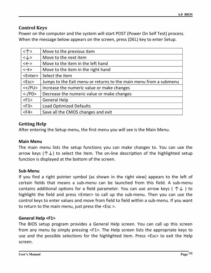
<↑> Move to the previous item
<↓> Move to the next item
<←> Move to the item in the left hand
<→> Move to the item in the right hand
<Enter> Select the item
<Esc> Jumps to the Exit menu or returns to the main menu from a submenu
<+/PU> Increase the numeric value or make changes
<‐/PD> Decrease the numeric value or make changes
<F1> General Help
<F3> Load Optimized Defaults
<F4> Save all the CMOS changes and exit
GettingHelpAfter entering the Setup menu, the first menu you will see is the Main Menu.
Main MenuThe main menu lists the setup functions you can make changes to. You can use thearrow keys (↑↓) to select the item. The on‐line descrip on of the highlighted setupfunction is displayed at the bottom of the screen.
Sub‐MenuIf you find a right pointer symbol (as shown in the right view) appears to the left ofcertain fields that means a sub‐menu can be launched from this field. A sub‐menucontains addi onal op ons for a field parameter. You can use arrow keys ( ↑↓ ) tohighlight the field and press <Enter> to call up the sub‐menu. Then you can use thecontrol keys to enter values and move from field to field within a sub‐menu. If you wantto return to the main menu, just press the <Esc >.
General Help <F1>The BIOS setup program provides a General Help screen. You can call up this screenfrom any menu by simply pressing <F1>. The Help screen lists the appropriate keys touse and the possible selections for the highlighted item. Press <Esc> to exit the Helpscreen.
User’s Manual Page 9898
6.0 BIOS
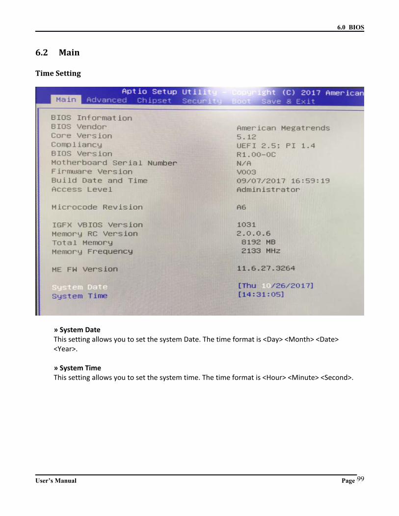
6.2 Main
TimeSetting
» System DateThis setting allows you to set the system Date. The time format is <Day> <Month> <Date> <Year>.
» System TimeThis setting allows you to set the system time. The time format is <Hour> <Minute> <Second>.
User’s Manual Page 9999

6.0 BIOS
6.3 Advanced
AMTConfiguration
SerialPortConfiguration
User’s Manual Page 100100

6.0 BIOS
» Serial Port 1/2/3/4 Enable or DisableSelect an Enable or Disable for the specified serial ports.
» COM1 RS232/422/485 Select
User’s Manual Page 101101

6.0 BIOS
» Watch Dog Function
User’s Manual Page 102102
6.0 BIOS
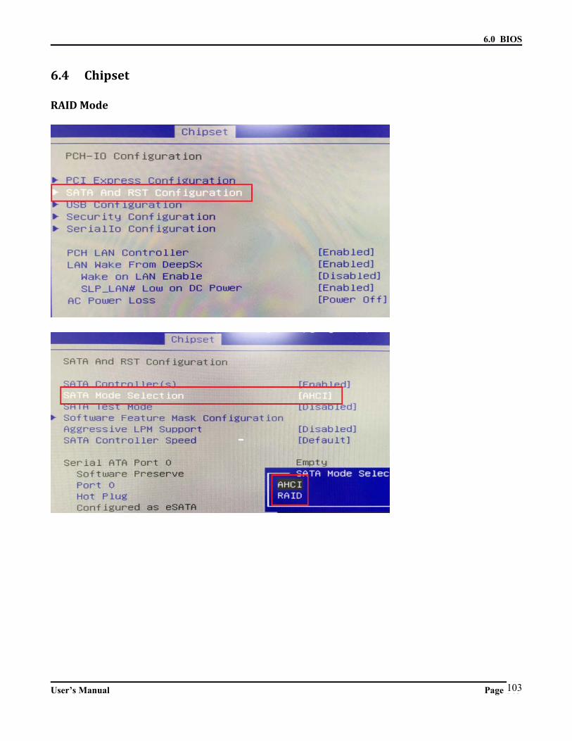
6.4 Chipset
RAIDMode
User’s Manual Page 103103
6.0 BIOS
User’s Manual Page 104104
6.0 BIOS
6.5 Boot
» 1st/2nd Boot DeviceThe items allow you to set the sequence of boot devices where BIOS attempts toload the disk operating system.
» Try Other Boot DevicesSetting the option to [Enabled] allows the system to try to boot from other device ifthe system fail to boot from the 1st/2nd boot device.
» Hard Disk Drives, CD/DVD Drives, USB DrivesThese settings allow you to set the boot sequence of the specified devices.
User’s Manual Page 105105

6.0 BIOS
User’s Manual Page 106106

7.0 Packing List
7.0PACKINGLIST
User’s Manual

7.0 Packing List
7.0 PACKINGLIST
7.1 PackingList
System
Item Part Number Module Name
1 765000040009 FleetPC‐9G1‐i7 System
2 765000040010 FleetPC‐9PG1‐i7 System
3 765000040015 FleetPC‐9G1‐C1 System
4 765000040016 FleetPC‐9PG1‐i7K System
Accessory
Picture Part Number Module Name Q’ty
326910027661 Cabling MC421‐350‐02G F 90D 1
326510051061 Cabling MC101‐508‐05GA1 F 90D 1
370850001000 FleetPC‐9 MOUNT BRACKET 2
351103040250 Screw F Type M3*4L ISO BK 4
User’s Manual Page 108