fpga handbook - pentek
TRANSCRIPT

PPPPPentek, Inc.entek, Inc.entek, Inc.entek, Inc.entek, Inc. • One Park Way, Upper Saddle River, NJ 07458 • Tel: (201) 818-5900 • Fax: (201) 818-5904 • Email: [email protected] • http://www.pentek.com
11111
Putting FPGAs to Work in Software Radio Systems
PPPPPentek, Inc.entek, Inc.entek, Inc.entek, Inc.entek, Inc.One Park Way, Upper Saddle River, New Jersey 07458
Tel: (201) 818-5900 • Fax: (201) 818-5904Email: [email protected] • http://www.pentek.com
Copyright © 2005, 2007, 2008, 2009, 2010, 2011, 2012, 2013, 2014, 2015, 2016, 2917, 2018 Pentek, Inc.Last Updated: October 2018
Contents of this publication may not be reproduced in any form without written permission.Specifications are subject to change without notice.
Pentek, GateFlow, ReadyFlow, SystemFlow, Cobalt, Onyx, Talon, Bandit, Flexor, GateXpress, SPARK, and QuickPac are trademarks or registered trademarks of Pentek, Inc.Other trademarks are properties of their respective owners.
TTTTTechnologyechnologyechnologyechnologyechnology
FPGA RFPGA RFPGA RFPGA RFPGA Resourcesesourcesesourcesesourcesesources
Optical ROptical ROptical ROptical ROptical Resourcesesourcesesourcesesourcesesources
PPPPProductsroductsroductsroductsroducts
ComplementarComplementarComplementarComplementarComplementary Py Py Py Py Productsroductsroductsroductsroducts
ApplicationsApplicationsApplicationsApplicationsApplications
by
RRRRRodger Hodger Hodger Hodger Hodger H. Hosking. Hosking. Hosking. Hosking. HoskingVice-President & Cofounder of Pentek, Inc.
®
Putting FPGAs to WPutting FPGAs to WPutting FPGAs to WPutting FPGAs to WPutting FPGAs to Work inork inork inork inork inSofSofSofSofSoftware Rtware Rtware Rtware Rtware Radio Systemsadio Systemsadio Systemsadio Systemsadio Systems
12th Edition

PPPPPentek, Inc.entek, Inc.entek, Inc.entek, Inc.entek, Inc. • One Park Way, Upper Saddle River, NJ 07458 • Tel: (201) 818-5900 • Fax: (201) 818-5904 • Email: [email protected] • http://www.pentek.com
22222
Putting FPGAs to Work in Software Radio Systems
Preface
FPGAs have become an increasingly important resource for software radio systems. Programmable logic technology now offerssignificant advantages for implementing software radio functions such as DDCs (Digital Downconverters). Over the past few
years, the functions associated with DDCs have seen a shift from being delivered in ASICs (Application-Specific ICs) to operatingas IP (Intellectual Property) in FPGAs.
For many applications, this implementation shift brings advantages that include design flexibility, higher precisionprocessing, higher channel density, lower power, and lower cost per channel. With the advent of each new, higher-performance
FPGA family, these benefits continue to increase.
This handbook introduces the basics of FPGA technology and its relationship to SDR (Software-Defined Radio) systems.A review of Pentek’s GateFlow FPGA Design Resources is followed by a discussion of features and benefits of FPGA-based DDCs.
Pentek SDR products that utilize FPGA technology and applications based on such products are also presented.
For more information on complementary subjects, the reader is referred to these Pentek Handbooks:
Critical Techniques for High-Speed A/D Converters in Real-Time Systems
High-Speed Switched Serial Fabrics Improve System Design
High-Speed, Real-Time Recording Systems
Putting VPX and OpenVPX to Work
Software-Defined Radio Handbook

PPPPPentek, Inc.entek, Inc.entek, Inc.entek, Inc.entek, Inc. • One Park Way, Upper Saddle River, NJ 07458 • Tel: (201) 818-5900 • Fax: (201) 818-5904 • Email: [email protected] • http://www.pentek.com
33333
Putting FPGAs to Work in Software Radio Systems
DIGITAL
MIXER
DIGITAL
LOCAL
OSC
DSP
DDC
Digital Downconverter
RF
TUNER
Analog
IF Signal
Analog
RF SignalA/D
CONV
Digital IF
Samples LOWPASS
FILTER
Digital
Baseband
Samples
TTTTTechnologyechnologyechnologyechnologyechnology
TTTTTypical Sofypical Sofypical Sofypical Sofypical Software Rtware Rtware Rtware Rtware Radio Systemadio Systemadio Systemadio Systemadio System SofSofSofSofSoftware Rtware Rtware Rtware Rtware Radio Tadio Tadio Tadio Tadio Tasksasksasksasksasks
We begin our discussion with the basic elements of asoftware radio receiver system.
The front end usually contains an analog RFamplifier and often an analog RF translator. Thistranslates the high frequency RF signals down to afrequency that an A/D converter can handle. This isusually below 200 MHz and is often an IF output.
The A/D output feeds the DDC (Digital Down-converter) stage, which is typically contained in a mono-lithic chip which forms the heart of a software radio system.
Notice, that after the signal is digitized by the A/Dconverter, all further operations are performed by digitalsignal-processing hardware.
Here we’ve ranked some of the popular signal-process-ing tasks associated with SDR systems on a two axisgraph, with compute Processing Intensity on the verticalaxis and Flexibility on the horizontal axis.
What we mean by process intensity is the degree ofhighly-repetitive and rather primitive operations. At theupper left are dedicated functions like A/D convertersand DDCs that require specialized hardware structuresto complete the operations in real time. ASICs are usuallychosen for these functions.
Flexibility pertains to the uniqueness or variabilityof the processing and how likely the function may haveto be changed or customized for any specific application.At the lower right are tasks like analysis and decision-making which are highly variable and often subjective.
Programmable general-purpose processors or DSPsare usually chosen for these tasks since these tasks can beeasily changed by software.
Now let’s temporarily step away from the softwareradio tasks and take a deeper look at programmablelogic devices.
Figure 1 Figure 2

PPPPPentek, Inc.entek, Inc.entek, Inc.entek, Inc.entek, Inc. • One Park Way, Upper Saddle River, NJ 07458 • Tel: (201) 818-5900 • Fax: (201) 818-5904 • Email: [email protected] • http://www.pentek.com
44444
Putting FPGAs to Work in Software Radio Systems
Early REarly REarly REarly REarly Roles for FPGAsoles for FPGAsoles for FPGAsoles for FPGAsoles for FPGAs LLLLLegacy FPGA Design Methodologiesegacy FPGA Design Methodologiesegacy FPGA Design Methodologiesegacy FPGA Design Methodologiesegacy FPGA Design Methodologies
TTTTTechnologyechnologyechnologyechnologyechnology
As true programmable gate functions becameavailable in the 1970’s, they were used extensively byhardware engineers to replace control logic, registers,gates and state machines which otherwise would haverequired many discrete, dedicated ICs.
Often these programmable logic devices were one-time factory-programmed parts that were soldered downand never changed after the design went into production.
These programmable logic devices were mostly thedomain of hardware engineers and the software toolswere tailored to meet their needs. You had tools foraccepting boolean equations or even schematics to helpgenerate the interconnect pattern for the growingnumber of gates.
Then, programmable logic vendors started offeringpredefined logic blocks for flip-flops, registers andcounters, that gave the engineer a leg up on popularhardware functions.
Nevertheless, the hardware engineer was stillintimately involved with testing and evaluating thedesign using the same skills he needed for testingdiscrete logic designs. He had to worry about propaga-tion delays, loading, clocking and synchronizing—alltricky problems that usually had to be solved the hardway—with oscilloscopes or logic analyzers.
Figure 3 Figure 4
� Tools were oriented to hardware engineers
� Schematic processors
� Boolean processors
� Gates, registers, counters, multipliers
� Successful designs required high-level
hardware engineering skills for:
� Critical paths and propagation delays
� Pin assignment and pin locking
� Signal loading and drive capabilities
� Clock distribution
� Input signal synchronization and skew analysis
� Used primarily to replace discrete digital
hardware circuitry for:
� Control logic
� Glue logic
� Registers and gates
� State machines
� Counters and dividers
� Devices were selected by hardware engineers
� Programmed functions were seldom changed
after the design went into production

PPPPPentek, Inc.entek, Inc.entek, Inc.entek, Inc.entek, Inc. • One Park Way, Upper Saddle River, NJ 07458 • Tel: (201) 818-5900 • Fax: (201) 818-5904 • Email: [email protected] • http://www.pentek.com
55555
Putting FPGAs to Work in Software Radio Systems
FPGAs: New Device TFPGAs: New Device TFPGAs: New Device TFPGAs: New Device TFPGAs: New Device Technologyechnologyechnologyechnologyechnology FPGAs: New Development TFPGAs: New Development TFPGAs: New Development TFPGAs: New Development TFPGAs: New Development Toolsoolsoolsoolsools
TTTTTechnologyechnologyechnologyechnologyechnology
Figure 5 Figure 6
� High Level Design Tools
� Block Diagram System Generators
� Schematic Processors
� High-level language compilers for
VHDL & Verilog
� Advanced simulation tools for modeling speed,
propagation delays, skew and board layout
� Faster compilers and simulators save time
� Graphically-oriented debugging tools
� IP (Intellectual Property) Cores
� FPGA vendors offer both free and licensed cores
� FPGA vendors promote third party core vendors
� Wide range of IP cores available
� 500+ MHz DSP slices and memory structures
Over 3500 dedicated on-chip hardware multipliers
On-board GHz serial transceivers
Partial reconfigurability maintains
operation during changes
Switched fabric interface engines
Over 690,000 logic cells
Gigabit Ethernet media access controllers
On-chip 405 PowerPC RISC microcontroller cores
Memory densities approaching 85 million bits
Reduced power with core voltages at 1 volt
Silicon geometries to 28 nanometers
High-density BGA and flip-chip packaging
Over 1200 user I/O pins
Configurable logic and I/O interface standards
�
�
�
�
�
�
�
�
�
�
�
�
�
It’s virtually impossible to keep up to date on FPGAtechnology, since new advancements are being madeevery day.
The hottest features are processor cores inside thechip, computation clocks to 500 MHz and above, andlower core voltages to keep power and heat down.
Several years ago, dedicated hardware multipliersstarted appearing and now you’ll find literally thousandsof them on-chip as part of the DSP initiative launchedby virtually all FPGA vendors.
High memory densities coupled with very flexiblememory structures meet a wide range of data flowstrategies. Logic slices with the equivalent of over tenmillion gates result from silicon geometries shrinkingbelow 0.1 micron.
BGA and flip-chip packages provide plenty of I/Opins to support on-board gigabit serial transceivers andother user-configurable system interfaces.
New announcements seem to be coming out everyday from chip vendors like Xilinx and Altera in a never-ending game of outperforming the competition.
To support such powerful devices, new design toolsare appearing that now open up FPGAs to both hard-ware and software engineers. Instead of just acceptinglogic equations and schematics, these new tools acceptentire block diagrams as well as VHDL and Verilogdefinitions.
Choosing the best FPGA vendor often hingesheavily on the quality of the design tools available tosupport the parts.
Excellent simulation and modeling tools help toquickly analyze worst case propagation delays andsuggest alternate routing strategies to minimize themwithin the part. This minimizes some of the trickytiming work for hardware engineers and can save onehours of tedious troubleshooting during design verifica-tion and production testing.
In the last few years, a new industry of third partyIP (Intellectual Property) core vendors now offer thou-sands of application-specific algorithms. These are readyto drop into the FPGA design process to help beat thetime-to-market crunch and to minimize risk.

PPPPPentek, Inc.entek, Inc.entek, Inc.entek, Inc.entek, Inc. • One Park Way, Upper Saddle River, NJ 07458 • Tel: (201) 818-5900 • Fax: (201) 818-5904 • Email: [email protected] • http://www.pentek.com
66666
Putting FPGAs to Work in Software Radio Systems
FPGAs for SDRFPGAs for SDRFPGAs for SDRFPGAs for SDRFPGAs for SDR FPGAs Bridge the SFPGAs Bridge the SFPGAs Bridge the SFPGAs Bridge the SFPGAs Bridge the SDRDRDRDRDR Application T Application T Application T Application T Application Task Spaceask Spaceask Spaceask Spaceask Space
TTTTTechnologyechnologyechnologyechnologyechnology
As a result, FPGAs have significantly invaded theapplication task space as shown by the center bubble inthe task diagram above.
They offer the advantages of parallel hardware tohandle some of the high process intensity functions likeDDCs and the benefit of programmability to accommo-date some of the decoding and analysis functions of DSPs.
These advantages may come at the expense ofincreased power dissipation and increased product costs.However, these considerations are often secondary to theperformance and capabilities of these remarkable devices.
Like ASICs, all the logic elements in FPGAs canexecute in parallel. This includes the hardware multipli-ers, and you can now get over 3500 of them on a singleFPGA.
This is in sharp contrast to programmable DSPs,which normally have just a handful of multipliers thatmust be operated sequentially.
FPGA memory can now be configured with thedesign tool to implement just the right structure fortasks that include dual port RAM, FIFOs, shift registersand other popular memory types.
These memories can be distributed along the signalpath or interspersed with the multipliers and mathblocks, so that the whole signal processing task operatesin parallel in a systolic pipelined fashion.
Again, this is dramatically different from sequentialexecution and data fetches from external memory as in aprogrammable DSP.
As we said, FPGAs now have specialized serial andparallel interfaces to match requirements for high- speedperipherals and buses.
Figure 7 Figure 8
� Parallel Processing
� Hardware Multipliers for DSP
� FPGAs can now have over 500 hardware multipliers
� Flexible Memory Structures
� Dual port RAM, FIFOs, shift registers, look up tables, etc.
� Parallel and Pipelined Data Flow
� Systolic simultaneous data movement
� Flexible I/O
� Supports a variety of devices, buses and interface standards
� High Speed
� Available IP cores optimized for special functions
PPPPPentek, Inc.entek, Inc.entek, Inc.entek, Inc.entek, Inc. • One Park Way, Upper Saddle River, NJ 07458 • Tel: (201) 818-5900 • Fax: (201) 818-5904 • Email: [email protected] • http://www.pentek.com
77777
Putting FPGAs to Work in Software Radio Systems
FPGA RFPGA RFPGA RFPGA RFPGA Resource Comparisonesource Comparisonesource Comparisonesource Comparisonesource Comparison
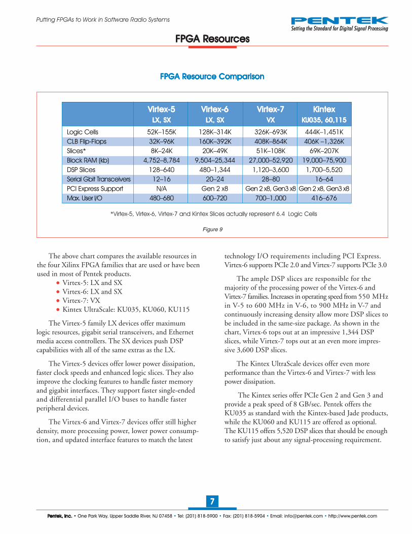
Figure 9
The above chart compares the available resources inthe four Xilinx FPGA families that are used or have beenused in most of Pentek products.
● Virtex-5: LX and SX● Virtex-6: LX and SX● Virtex-7: VX● Kintex UltraScale: KU035, KU060, KU115
The Virtex-5 family LX devices offer maximumlogic resources, gigabit serial transceivers, and Ethernetmedia access controllers. The SX devices push DSPcapabilities with all of the same extras as the LX.
The Virtex-5 devices offer lower power dissipation,faster clock speeds and enhanced logic slices. They alsoimprove the clocking features to handle faster memoryand gigabit interfaces. They support faster single-endedand differential parallel I/O buses to handle fasterperipheral devices.
The Virtex-6 and Virtex-7 devices offer still higherdensity, more processing power, lower power consump-tion, and updated interface features to match the latest
*Virtex-5, Virtex-6, Virtex-7 and Kintex Slices actually represent 6.4 Logic Cells
VirVirVirVirVirtex-5tex-5tex-5tex-5tex-5 VirVirVirVirVirtex-6tex-6tex-6tex-6tex-6 VirVirVirVirVirtex-7tex-7tex-7tex-7tex-7 KintexKintexKintexKintexKintexLX, SXLX, SXLX, SXLX, SXLX, SX LX, SXLX, SXLX, SXLX, SXLX, SX VXVXVXVXVX KKKKKU035, 60,115U035, 60,115U035, 60,115U035, 60,115U035, 60,115
Logic Cells 52K–155K 128K–314K 326K–693K 444K–1,451KCLB Flip-Flops 32K–96K 160K–392K 408K–864K 406K –1,326KSlices* 8K–24K 20K–49K 51K–108K 69K–207KBlock RAM (kb) 4,752–8,784 9,504–25,344 27,000–52,920 19,000–75,900DSP Slices 128–640 480–1,344 1,120–3,600 1,700–5,520Serial Gbit Transceivers 12–16 20–24 28–80 16–64PCI Express Support N/A Gen 2 x8 Gen 2 x8, Gen3 x8 Gen 2 x8, Gen3 x8Max. User I/O 480–680 600–720 700–1,000 416–676
FPGA RFPGA RFPGA RFPGA RFPGA Resourcesesourcesesourcesesourcesesources
technology I/O requirements including PCI Express.Virtex-6 supports PCIe 2.0 and Virtex-7 supports PCIe 3.0
The ample DSP slices are responsible for themajority of the processing power of the Virtex-6 andVirtex-7 families. Increases in operating speed from 550 MHzin V-5 to 600 MHz in V-6, to 900 MHz in V-7 andcontinuously increasing density allow more DSP slices tobe included in the same-size package. As shown in thechart, Virtex-6 tops out at an impressive 1,344 DSPslices, while Virtex-7 tops out at an even more impres-sive 3,600 DSP slices.
The Kintex UltraScale devices offer even moreperformance than the Virtex-6 and Virtex-7 with lesspower dissipation.
The Kintex series offer PCIe Gen 2 and Gen 3 andprovide a peak speed of 8 GB/sec. Pentek offers theKU035 as standard with the Kintex-based Jade products,while the KU060 and KU115 are offered as optional.The KU115 offers 5,520 DSP slices that should be enoughto satisfy just about any signal-processing requirement.

PPPPPentek, Inc.entek, Inc.entek, Inc.entek, Inc.entek, Inc. • One Park Way, Upper Saddle River, NJ 07458 • Tel: (201) 818-5900 • Fax: (201) 818-5904 • Email: [email protected] • http://www.pentek.com
88888
Putting FPGAs to Work in Software Radio Systems
� Allows FPGA design engineers to easily add
functions to standard factory configuration
� Includes VHDL source code for all standard functions:
� Control and status registers
� A/D and Digital receiver interfaces
� Mezzanine interfaces
� Triggering, clocking, sync and gating functions
� Data packing and formatting
� Channel selection
� A/D / Receiver multiplexing
� Interrupt generation
� Data tagging and channel ID
� User Block for inserting custom code
Figure 10 Figure 11
GateFlow FPGA Design RGateFlow FPGA Design RGateFlow FPGA Design RGateFlow FPGA Design RGateFlow FPGA Design Resourcesesourcesesourcesesourcesesources GateFlow FPGA Design KitGateFlow FPGA Design KitGateFlow FPGA Design KitGateFlow FPGA Design KitGateFlow FPGA Design Kit
FPGA RFPGA RFPGA RFPGA RFPGA Resourcesesourcesesourcesesourcesesources
GateFlow
FPGA
Design
Kit
GateFlow
Factory
Installed
IP Cores
If you want to add your own algorithms to Pentekcatalog products, we offer the GateFlow FPGA DesignKit that includes VHDL source code for all the standardfactory functions.
VHDL is one of the most popular languages used inthe FPGA design tools. The GateFlow Design Kit includesthe VHDL source code for every software module we useto create these standard factory features of the product.
The standard factory configuration supports a widerange of operating modes, timing and sync functions, aswell as several different data formatting options.
This includes control and status registers, peripheralinterfaces, mezzanine interfaces, timing functions, dataformatting, channel selection, interrupt support, anddata tagging.
These are also fully supported with our ReadyFlowBoard Support Package.
GateFlow® is Pentek’s flagship collection of FPGADesign Resources. The GateFlow line is compatible withthe Xilinx Virtex products and is available as twoseparate offerings:
If you want to add your own custom algorithms, weoffer the GateFlow FPGA Design Kit.
We also offer popular high-performance signal-process-ing algorithms with the GateFlow factory-installed IPCores. These algorithms are designed and optimizedexpressly for Xilinx FPGAs and Pentek hardware products.
Installed Cores are delivered to you preinstalled inyour Pentek FPGA-based product of choice and are fullysupported with Pentek ReadyFlow® Board SupportPackages.
Let’s start with the GateFlow FPGA Design Kit.

PPPPPentek, Inc.entek, Inc.entek, Inc.entek, Inc.entek, Inc. • One Park Way, Upper Saddle River, NJ 07458 • Tel: (201) 818-5900 • Fax: (201) 818-5904 • Email: [email protected] • http://www.pentek.com
99999
Putting FPGAs to Work in Software Radio Systems
FPGA RFPGA RFPGA RFPGA RFPGA Resourcesesourcesesourcesesourcesesources
GateFlow FPGA Design Kit for Cobalt, Onyx, Jade and Flexor PGateFlow FPGA Design Kit for Cobalt, Onyx, Jade and Flexor PGateFlow FPGA Design Kit for Cobalt, Onyx, Jade and Flexor PGateFlow FPGA Design Kit for Cobalt, Onyx, Jade and Flexor PGateFlow FPGA Design Kit for Cobalt, Onyx, Jade and Flexor Productsroductsroductsroductsroducts
Front Panel Interface
Memory
Controller
MemoryController
Sync Bus
Interface
PCI Express Interface
Global Registers
FLASH Interface
ClockGenerator
Timestamp
TestGenerator
PCI Express Backend
MemoryController
Memory
Controller
V-6 or V-7-
FPGA
User Application Container
Defined and
documented
interface signals
Board
RegistersUser
Registers
DMAs P14
LVDS
P16
MGTs
Factory Installed
Base Function Application
A/D & D/A Control
Data Packing & Formatting
Meta Data Files
Linked-List A/D Control
Linked-List D/A Control
Figure 12
The GateFlow FPGA Design Kit allows the user tomodify, replace and extend the standard factory-installedfunctions in the FPGA to incorporate special modes ofoperation, new control structures, and specialized signal-processing algorithms.
The Cobalt, Onyx and Flexor architectures config-ure the FPGA with standard factory-supplied interfacesincluding memory controllers, DMA engines, A/Dand D/A interfaces, timing and synchronizationstructures, triggering and gating logic, time stampingand header tagging, data formatting engines, and thePCIe interface. These resources are connected to the UserApplication Container using well-defined ports that presenteasy-to-use data and control signals, effectively abstract-ing the lower level details of the hardware.
Shown here is the FPGA block diagram of a typicalCobalt, Onyx, Jade or Flexor module. The User Applica-tion Container holds a collection of different factory-installedIP modules connected to the various interfaces throughthe standard ports surrounding the container. The specificIP modules for each product are described in further detailin the datasheet of that product.
The GateFlow Design Kit provides a completeXilinx ISE Foundation or Vivado project foldercontaining all the files necessary for the FPGA devel-oper to recompile the entire project with or without anyrequired changes. VHDL source code for each moduleprovides an example of how the IP modules work, howthey might be modified, and how they might be replacedwith custom IP to implement a specific function.

PPPPPentek, Inc.entek, Inc.entek, Inc.entek, Inc.entek, Inc. • One Park Way, Upper Saddle River, NJ 07458 • Tel: (201) 818-5900 • Fax: (201) 818-5904 • Email: [email protected] • http://www.pentek.com
1010101010
Putting FPGAs to Work in Software Radio Systems
PPPPPentek Navigatorentek Navigatorentek Navigatorentek Navigatorentek Navigator
PPPPProductsroductsroductsroductsroducts
Figure 13
Pentek’s Navigator Design Suite includes theNavigator FDK (FPGA Design Kit) for integratingcustom IP into the Pentek factory-shipped design andthe Navigator BSP (Board Support Package) for creatinghost applications. The Navigator Design Suite takes anew approach to solving FPGA IP and control softwareconnectivity.
Most modern FPGA-processing applications requiredevelopment of specialized FPGA IP to run on the hard-ware, and software to control the FPGA hardware from ahost computer.
Even when “turnkey” solutions are delivered withcomplete FPGA IP and software libraries, as develop-ers add their own custom-processing IP, new softwareneeds to be created to control the custom IP functions.
Problems often arise when the IP and softwaredevelopment tools treat application development as twoseparate tasks. Changes to FPGA IP and control softwarecan quickly get out of sync, complicating new applicationdevelopment or even breaking the formally functioningturnkey components.
The Navigator Design Suite was designed from theground up to work with Pentek’s JadeTM architectureand provide a better solution to the complex task of IP andsoftware creation.
As FPGAs become larger and IP more complex,the need for IP design tools to manage this growingcomplexity has never been greater.
The Xilinx Vivado Design Suite includes IP Integrator,the industry’s first plug-and-play IP integration designenvironment. Built around a graphical block diagraminterface, IP Integrator allows IP developers to leverageexisting IP by importing it into their block diagramdesign. Pentek’s Navigator FPGA Design Kit (FDK),was designed with this exact purpose.
Each Navigator FDK provides the complete IP for aspecific Jade data acquisition and processing board. Whenthe design is opened in Vivado’s IP Integrator, thedeveloper can access every component of the Pentek design,replacing or modifying blocks as needed for the applica-tion. All blocks use industry standard AXI4 interfacesproviding a well-defined format for custom IP to connect tothe rest of the design. Each Navigator/Jade design includesUser Blocks in the data-flow path, ideal for inserting customprocessing IP.
The Navigator FDK includes complete documenta-tion, test benches and full VHDL source for developerswho desire complete access to the IP. In addition to theIP specific to the supported Jade board, Navigator alsoincludes processing blocks for some of the most commonlyused algorithms. ➤

PPPPPentek, Inc.entek, Inc.entek, Inc.entek, Inc.entek, Inc. • One Park Way, Upper Saddle River, NJ 07458 • Tel: (201) 818-5900 • Fax: (201) 818-5904 • Email: [email protected] • http://www.pentek.com
1111111111
Putting FPGAs to Work in Software Radio Systems
PPPPProductsroductsroductsroductsroducts
Figure 14
The companion product to the Navigator FDK is thePentek Navigator Board Support Package (BSP). WhileNavigator FDK provides a streamlined path for creatingor modifying new IP for the Pentek hardware, the NavigatorBSP enables complete operational control of the hardwareand all IP functions in the FPGA.
Similar to the FDK, the BSP allows softwaredevelopers to work at a higher level, abstracting manyof the details of the hardware through an intuitive API.The API allows developers to focus on the task of creatingthe application by letting the API, the hardware and IP-control libraries below it to handle many of the board-specificfunctions. Developers who want full access to the entireBSP library, enjoy complete C-language source code as wellas full documentation.
New applications can be developed on their own orby building on one of the included example programs.All Jade boards are shipped with a full suite of build-infunctions allowing operation without the need for anycustom IP development. Many users find these functionsideal for addressing their application requirements.
The Navigator BSP includes the Signal Analyzer,a full-featured analysis tool, that displays data in timeand frequency domains. Built-in measurement functionsdisplay 2nd and 3rd harmonics, THD (total harmonicdistortion), and SINAD (signal to noise and distortion).Interactive cursors allow users to mark data points andinstantly calculate amplitude and frequency of displayedsignals. With the Signal Analyzer users can install the Pentekhardware and Navigator BSP and start viewing analog signalsimmediately.
PPPPPentek Navigatorentek Navigatorentek Navigatorentek Navigatorentek Navigator

PPPPPentek, Inc.entek, Inc.entek, Inc.entek, Inc.entek, Inc. • One Park Way, Upper Saddle River, NJ 07458 • Tel: (201) 818-5900 • Fax: (201) 818-5904 • Email: [email protected] • http://www.pentek.com
1212121212
Putting FPGAs to Work in Software Radio Systems
GateFlow Installed IP CoresGateFlow Installed IP CoresGateFlow Installed IP CoresGateFlow Installed IP CoresGateFlow Installed IP Cores
Figure 15
� Pentek Installs IP Cores in Pentek Products
� Cores are tailored and optimized for:
� Specific devices and I/O found on Pentek products
� Efficient FPGA resource utilization
� Execution and throughput speed
� Eliminates need for customer FPGA development
� Fully supported with ReadyFlow Board Support Libraries
Pentek is an AllianceCore Member, a third partyprogram sponsored by Xilinx for companies that special-ize in specific areas of expertise in developing FPGAalgorithms for niche application areas. These includeimage processing, communications, telecom, telemetry,signal intelligence, wireless communications, wirelessnetworking, and many other disciplines.
Pentek offers popular high-performance signalprocessing algorithms installed in Pentek products. Thesealgorithms are designed expressly for Xilinx FPGAs andPentek harware products. The cores take full advantageof the numerous hardware multipliers to achieve highly-parallel processing structures that can dramaticallyoutperform programmable RISC and DSP processors.
Installed Cores are optimized for efficient FPGAresource utilization, execution and throughput speed.They are delivered to you preinstalled in your PentekFPGA-based product of choice and are fully tested andsupported with the Pentek ReadyFlow Board SupportPackages. Purchasing these popular factory-installedcores saves you the time and costs of acquiring FPGAtools and developing custom FPGA code.
FPGA RFPGA RFPGA RFPGA RFPGA Resourcesesourcesesourcesesourcesesources

PPPPPentek, Inc.entek, Inc.entek, Inc.entek, Inc.entek, Inc. • One Park Way, Upper Saddle River, NJ 07458 • Tel: (201) 818-5900 • Fax: (201) 818-5904 • Email: [email protected] • http://www.pentek.com
1313131313
Putting FPGAs to Work in Software Radio Systems
Figure 16
Digital DownconverDigital DownconverDigital DownconverDigital DownconverDigital Downconverter Fter Fter Fter Fter Fundamentalsundamentalsundamentalsundamentalsundamentals
CICInitial
Downsample
CICCoarse Gain
CFIRPolyphaseDecimator
PFIRPolyphaseDecimator
Roundin
g
DDSNCO
Signal In
COMPLEXDIGITALMIXER I
Q
FilterCoefficients
Tuning Stage Data Reduction Gain Adjustment Additional Data Reductionand Signal Shaping
FilterCoefficients
SIN COS
TuningFrequency
Signal Out
Over the past few years, the functions associatedwith DDCs have seen a shift from being delivered inASICs (Application-Specific ICs) to operating as IP(Intellectual Property) in FPGAs.
For many applications, this implementation shiftbrings advantages that include: design flexibility, higher-precision processing, higher channel density, lowerpower, and lower cost per channel. With the advent ofeach new higher performance FPGA family during thepast few years, these benefits continue to increase.
To understand how FPGAs play a key role inimplementing DDCs that perform the function of areceiver, it’s important to break the DDC down into itsindividual functional blocks. The block diagram shows aclassic DDC. Regardless of whether it’s implemented inan ASIC or an FPGA, this is the common architectureof the DDC function.
The first stage of the DDC uses a complex digitalmixer to translate the frequency of interest down tobaseband. It uses a pair of multipliers and a DDS(Direct Digital Synthesizer) as the NCO (NumericallyControlled Oscillator). This function enables the user totune the receiver to the desired frequency of interest.The second stage of the DDC reduces the samplingfrequency of the signal to match the desired outputbandwidth. It uses a CIC (Cascaded Integrator Comb)filter to decimate the data.
A second CIC filter provides a coarse gain adjustmentstage. The signal is then passed to a pair of additionalpolyphase filters. First a CFIR (Compensation FiniteImpulse Response) filter then to a PFIR (ProgrammableFinite Impulse Response) filter. This filter pair providesadditional decimation and final signal shaping prior tothe rounding stage and final output.
When we get past all the acronyms, we realize thatmost of the individual function blocks of the DDC areimplemented using multipliers. It thus becomes apparenthow the DDC might map into current FPGA families.Most new FPGAs include a wealth of DSP functionblocks which are primarily multipliers. The general-purpose logic resource and on-chip memory of FPGAsalso match the requirements of the DDC for implement-ing the required FIR filters and filter coefficient tables.
As part of their IP library series, Xilinx provides afree DDC core. The core serves as a good generalreference design, following the classic DDC architectureshown here. While this core can be used as a buildingblock for general purpose DDCs, the real advantages ofan IP-based implementation can be best seen in optimizedcustom cores that are designed to match the requirementsof a specific application.
Pentek offers a series of high-performance IP-basedDDCs and DUCs available preinstalled in their softwareradio boards. Each is optimized to match a specific rangeof application requirements.
FPGA RFPGA RFPGA RFPGA RFPGA Resourcesesourcesesourcesesourcesesources
➤

PPPPPentek, Inc.entek, Inc.entek, Inc.entek, Inc.entek, Inc. • One Park Way, Upper Saddle River, NJ 07458 • Tel: (201) 818-5900 • Fax: (201) 818-5904 • Email: [email protected] • http://www.pentek.com
1414141414
Putting FPGAs to Work in Software Radio Systems
These cores range from a 3-channel core installedin the Model 71621 with triple 200 MHz A/D, to the1100-channel GSM channelizer core installed in theModel 71663 with quad 200 MHz A/D.
These two and many other FPGA-based SDRproducts are available in industry-standard PMC/XMCmodules as well as CompactPCI, PCI Express, AMC andOpenVPX formats.
When compared on a size/power/cost per channelbasis, narrowband, high-channel-count DDC corescan be very efficiently implemented in FPGAs.Implementation of wideband DDCs consumes manymore FPGA DSP and logic resources. As a result, thenumber of channels that can be fit into a single FPGA islimited. Even with less cost-effective wideband DDCs,
IP Enables SofIP Enables SofIP Enables SofIP Enables SofIP Enables Software Rtware Rtware Rtware Rtware Radio Padio Padio Padio Padio Productsroductsroductsroductsroducts
the custom IP approach can usually provide the onlyviable solution when a specific performance character-istic is required.
An additional benefit of IP-based solutions is theflexible nature of their implementation. These productsare created by using the same hardware base with differentinstalled IP cores. They all share the same software baseallowing migration between different applications to beaccomplished with minimum software porting.
Again, this wide range of applications can besatisfied by using a small set of hardware with different,optimized IP cores. This is one of the fundamentalconcepts of SDR (Software-Defined Radio), and it’sdifficult, if not impossible, to achieve with ASIC-basedsolutions.
FPGA RFPGA RFPGA RFPGA RFPGA Resourcesesourcesesourcesesourcesesources

PPPPPentek, Inc.entek, Inc.entek, Inc.entek, Inc.entek, Inc. • One Park Way, Upper Saddle River, NJ 07458 • Tel: (201) 818-5900 • Fax: (201) 818-5904 • Email: [email protected] • http://www.pentek.com
1515151515
Putting FPGAs to Work in Software Radio Systems
Figure 17
The above chart shows the salient characteristics forPentek’s SDR products with factory-installed IP cores. All ofthese products are available off-the-self and are in the Pentekdatasheets and catalogs. The chart provides informationregarding the number of input channels, maximumsampling frequency of their A/Ds, and the number of bits.This information is followed by DDC characteristics suchas number of DDC channels and the decimation range.
PPPPPentek Pentek Pentek Pentek Pentek Products with Froducts with Froducts with Froducts with Froducts with Factoractoractoractoractoryyyyy-Installed SDR IP Cores-Installed SDR IP Cores-Installed SDR IP Cores-Installed SDR IP Cores-Installed SDR IP Cores
Other information that’s specific to each core isincluded as well as an indication of the models that includea DUC, an interpolation filter and output D/A. As shownin the chart, many of these models include features that arecritical for beamforming and direction-finding applications.All the models shown are XMC modules. As with allPentek SDR products, these models are also available inPCI Express, VPX, AMC, and CompactPCI formats.
InputInputInputInputInput SamplingSamplingSamplingSamplingSampling InputInputInputInputInput DDCDDCDDCDDCDDC DecimationDecimationDecimationDecimationDecimation OutputOutputOutputOutputOutput DUCDUCDUCDUCDUC Interpol.Interpol.Interpol.Interpol.Interpol. ChanChanChanChanChan..... OutOutOutOutOut Beam-Beam-Beam-Beam-Beam-
ModelModelModelModelModel ChannelsChannelsChannelsChannelsChannels FFFFFreq (max)req (max)req (max)req (max)req (max) BitsBitsBitsBitsBits ChanChanChanChanChan..... RRRRRangeangeangeangeange BitsBitsBitsBitsBits ChanChanChanChanChan..... RRRRRangeangeangeangeange OutOutOutOutOut BitsBitsBitsBitsBits formerformerformerformerformer
71621 3 200 MHz 16 3 2–64K 16 or 24 1 2–512K 2 16 Yes
71721 3 200 MHz 16 3 2–64K 16 or 24 1 2–512K 2 16 Yes
71131 8 250 MHz 16 8 2–32K – None None None – No
71821 3 200 MHz 16 3 2–32K 16 or 24 2 2–262K 2 16 No
71624* 2 200 MHz 16 34 512–8192 16 34 512–8192 2 – No
71641 1 or 2 3.6 or 1.8 GHz 12 1 or 2 4, 8 or 16 16 None None None – No
71741 1 or 2 3.6 or 1.8 GHz 12 1 or 2 4, 8 or 16 16 None None None – No
71841 1 or 2 3.6 or 1.8 GHz 12 1 or 2 4, 8 or 16 16 None None None – No
71651 2 500/400 MHz 12/14 2 2–128K 16 or 24 1 2–512K 2 16 Yes
71751 2 500/400 MHz 12/14 2 2–128K 16 or 24 1 2–512K 2 16 Yes
71851 2 500/400 MHz 12/14 2 2–128K 16 or 24 1 2–512K 2 16 Yes
71661 4 200 MHz 16 4 2–64K 16 or 24 None None None – Yes
71861 4 200 MHz 16 4 2–32K 16 or 24 None None None – Yes
71662 4 200 MHz 16 32 16–8K 24 None None None – No
71663 4 200 MHz 16 1100 – – None None None – No
71664** 4 200 MHz 16 4 2–64K 16 or 24 None None None – Yes
71671 None None – None – – 4 2–1024K 4 16 No
71771 None None – None – – 4 2–1024K 4 16 No
Notes: Products use Virtex-6 FPGAs except: 71721, 71741, 71751, and 71771 which use Virtex-7 FPGAs
* Adaptive relay performance 71131, 71821, 71841, 71851, and 71861 which use Kintex FPGAs
** Meets VITA 49.0 specification
FPGA RFPGA RFPGA RFPGA RFPGA Resourcesesourcesesourcesesourcesesources

PPPPPentek, Inc.entek, Inc.entek, Inc.entek, Inc.entek, Inc. • One Park Way, Upper Saddle River, NJ 07458 • Tel: (201) 818-5900 • Fax: (201) 818-5904 • Email: [email protected] • http://www.pentek.com
1616161616
Putting FPGAs to Work in Software Radio Systems
Optical ROptical ROptical ROptical ROptical Resourcesesourcesesourcesesourcesesources
Property Copper OpticalInterface Transceiver Cost Low High but dropping
PC Network Interface Cards Integrated in PC or laptop Usually optional at $100-$200
Power over Ethernet Supported at low cost Not possible
Data Rate 1 GHz >10 GHz
Cable Loss - 100 meters 94% 3%
Max Transmission Distance 100 m (cat 6) 300 m (multi-mode)10 km (single mode)
EMI Susceptibility Risk Moderate Zero
EMI Radiation Risk Moderate Zero
Security / Eavesdropping Risk High Extremely Low
Termination Costs Low High
Cable Cost per Length High Low
Cable Weight per 1000 m 60 to 600 kg 6 kg
Fire Hazard Supports current flow if shorted Zero
Tensile Strength 25 pounds 100-250 pounds
Cleaning Requirements No Yes
Optical Links Offer Many BenefitsOptical Links Offer Many BenefitsOptical Links Offer Many BenefitsOptical Links Offer Many BenefitsOptical Links Offer Many Benefits
Figure 18
One major shortcoming of copper cable is signal loss,which becomes a serious limitation for higher frequencysignals and longer cable lengths. Across a span of 100meters, optical cables can sustain data rates up to 100 timeshigher than copper cable.
Because copper cables radiate electromagnetic energy,eavesdropping on network cables is a major security concern,not only for military and government customers, butalso for corporations, banks, and financial institutions.Advanced signal sniffers in vehicles and briefcases arehard to detect and restrict. Optical cables are extremelydifficult to “tap” without damaging the cable, resultingin immediate detection.
Signals flowing in copper cables are also susceptibleto contamination from nearby sources of electromagneticradiation, such as antennas, generators, and motors. Thisis critical for military and commercial aircraft and ships,as well as manned or unmanned vehicles, which are oftenpacked with dozens of different electronic payloads. Opticalcables are completely immune to EMI.
Physically, optical cables are much smaller and lighterthan copper cables, especially important for weight-sensitiveapplications such as weapons, unmanned vehicles, and aircraft.Optical cables will operate just as well when submerged inseawater, and are completely immune to electrical shorting,especially important where explosive vapors may be present.To ease installation through conduits and passages, opticalcables have smaller diameters and can withstand up to tentimes more pulling tension than copper cables.
Driven by huge commercial markets for data servers,storage networks, telecom systems, and home or officeinternet and entertainment systems, optical interfaces arereplacing older copper connections for good reasons: costand performance. As the use of optical cables becomesmore widespread, the cost per length can be muchlower than copper cables that depend on commoditymetal pricing. As is often the case, industrial, militaryand government embedded systems are now takingadvantage of the many benefits of this rapidly advanc-ing commercial technology.

PPPPPentek, Inc.entek, Inc.entek, Inc.entek, Inc.entek, Inc. • One Park Way, Upper Saddle River, NJ 07458 • Tel: (201) 818-5900 • Fax: (201) 818-5904 • Email: [email protected] • http://www.pentek.com
1717171717
Putting FPGAs to Work in Software Radio Systems
Optical ROptical ROptical ROptical ROptical Resourcesesourcesesourcesesourcesesources
An optical cable is a waveguide for propagating lightthrough an optical fibre. It consists of a central core cladwith a dielectric material having a higher index ofrefraction than the core to ensure total internal reflec-tion. Optical cables use either multi-mode or single-mode transmission.
Multi-mode cables accept light rays entering the corewithin a certain angle of the axis. They travel down thecable by repeatedly reflecting off the dielectric boundarybetween the core and the cladding. The core diametersare typically 50 or 62.5 mm, and the wavelength of lightis typically 850 nm.
Single-mode cables propagate light as an electromag-netic wave operating in a single transverse mode straightdown the fibre using typical wavelengths of 1310 and1550 nm. The core diameter must be no greater than tentimes the light wavelength, typically 8 to 10 µm. Althoughsingle-mode cables can carry signals over lengths 10 to100 times longer than multi-mode, the transceivers aremore expensive.
Optical CablesOptical CablesOptical CablesOptical CablesOptical Cables
Hundreds of different types of optical cable connec-tors exist in the market, each addressing specific applica-tions and environments. The challenge is connecting theends of two optical cables to retain the maximum fidelity ofthe light interface, in spite of human factors, tolerances,contamination, and environments. Special tools and kitsfor cleaning the ends of each optical fibre are essentialfor reliable operation.
Optical TOptical TOptical TOptical TOptical Transceiversransceiversransceiversransceiversransceivers
Coupling electrical signals to light signals for transmis-sion through optical cables requires optical transceivers. Mostsystems require full-duplex operation for each optical link tosupport flow-control and error correction. A pair of opticalfibers, often bonded together in the same cable, supportstransmit and receive data flowing in opposite directions.
Although several analog light modulation schemes (includ-ing AM and FM) have been used in the past, now almost alltransceivers use digital modulation. Optical emitters simplytranslate the digital logic levels into on/off modulation of the laserlight beam, while the detectors convert the modulated light backinto digital signals. This physical layer interface for transporting0s and1s is capable of supporting any protocol.
The latest transceivers use laser emitters to supportdata rates to 100 Gbits/sec and higher, and each genera-tion steadily reduces the power, size and cost of devices.Different technologies are required for emitters and detectors,but both are often combined in a single product to providefull-duplex operation.
Optical transceivers thus provide a physical layerinterface between optical cables and the vast array ofelectrical multi-gigabit serial ports found on processors,FPGAs, and network adapters. As a result, optical transceiv-ers are transparent to the protocols they support, makingthem appropriate for any high-speed serial digital link.
Electrical signals of the optical transceivers connectto the end point device, which must then handle clockencoding and recovery, synchronization, and line balanceat the physical layer. Data link layer circuitry establishesframing so that data words can be sent and received acrossthe channel.
Figure 19
The Pentek Model 52611 Quad SerialFPDP 3U VPX modulesupports four full-duplex LC optical cables for connections
between chassis, each operating at over 400 MB/sec

PPPPPentek, Inc.entek, Inc.entek, Inc.entek, Inc.entek, Inc. • One Park Way, Upper Saddle River, NJ 07458 • Tel: (201) 818-5900 • Fax: (201) 818-5904 • Email: [email protected] • http://www.pentek.com
1818181818
Putting FPGAs to Work in Software Radio Systems
Optical ROptical ROptical ROptical ROptical Resourcesesourcesesourcesesourcesesources
Choosing the Right Optical PChoosing the Right Optical PChoosing the Right Optical PChoosing the Right Optical PChoosing the Right Optical Protocolrotocolrotocolrotocolrotocol
Protocols define the rules and features supported by eachtype of system link, ranging from simple transmission of rawdata to sophisticated multi-processor support for distributednetworks, intelligent routing, and robust error correction. Ofcourse, heavier protocols invariably mean less efficient datatransfers and increased latency. Generally, it is best to use thesimplest protocol that satisfies the system requirements.
As an example of a lightweight protocol, Aurora for XilinxFPGAs features on-board link-layer engines and high-speedserial transceivers. Aurora is intended primarily for point-to-point connectivity for sending data between two FPGAs. Itincludes 8b/10b or 64b/66b channel coding to balance thetransmission channel, and supports single- or full-duplexoperation. Aurora handles virtually any word length and allowsmultiple serial lanes to be bonded into a single logical channel,aggregating single lane bit rates for higher data throughput.Data rates for each serial lane can be 12.5 Gbits/sec or higher.Extremely simple and with minimal overhead, Aurora is veryefficient in linking data streams between multiple FPGAswithin a module, or between modules across a backplane.
Stepping up in complexity is the SerialFPDP protocoldefined under VITA 17.1 It addresses several importantneeds of embedded systems including flow control to avoiddata overruns, and copy mode to allow one node to receivedata and also forward it on to another node. The copy/loopmode supports a ring of multiple nodes eventually complet-ing a closed loop. The nominal data rate on each lane is2.5 Gbits/sec, but advances in device technology now supportrates over twice that speed.
Infiniband defines a flexible, low-latency, point-to-point interconnect fabric for data storage and servers withcurrent rates of 14 Gbits/sec, moving up to 50 Gbits/sec inthe next few years. Channel speeds can be boosted by forminglogical channels by bonding 4 or 12 lanes.
The venerable Ethernet protocol still dominatescomputer networks, with 10GbE now commonly supportedby a vast range of computers, switches, and adapters. Eventhough Ethernet suffers from high overhead, making itsomewhat cumbersome for high-data rate low-latencyapplications, its ubiquitous presence virtually assurescompatibility.
VITVITVITVITVITA 49.0: VITA 49.0: VITA 49.0: VITA 49.0: VITA 49.0: VITA RA RA RA RA Radio Tadio Tadio Tadio Tadio Transporransporransporransporransport (VRT) Standardt (VRT) Standardt (VRT) Standardt (VRT) Standardt (VRT) Standard
Figure 20
New extensions to the VITA VRT Protocol define standardizedpackets for control and status of radio receiver and transmitter
equipment and digitized receive and transmit signalpayload packets for added flexibility
Approved as an ANSI standard in 2007, VITA 49.0defines standardized packets for connecting softwareradio systems for communications, radar, telemetry,direction finding, and other applications. The originalspecification addressed only receiver functions. Receivesignal data packets deliver digitized payload data, aprecise time stamp, and identifiers for each channel andsignal. Context packets include operating parameters ofthe receiver including tuning frequency, bandwidth,sampling rate, gain, antenna orientation, speed, heading,etc. One notable shortcoming of the original specifica-tion was its inability to control the receiver.
VITA 49.2, a new extension to VRT now in ballot-ing, adds control packets for delivering operationalparameters to all aspects of the radio equipment, as wellas support for transmitters. The new stimulus packetscontain streaming digital samples of signals to be transmit-ted. Other new packets, called capabilities packets, inform thehost control system of the available hardware in the radioalong with the allowed range of parameters for control.Lastly, spectrum packets from the receiver deliver spectralinformation to help simplify spectral survey and energydetection operations required by the control system.
With this latest extension, VRT provides a standard-ized protocol for controlling and configuring all aspectsof a software-radio transceiver. One major objective isenabling a common radio hardware platform to handle awide range of applications simply by implementing newhost software algorithms that exploit VRT protocols toachieve the required modes of operation.

PPPPPentek, Inc.entek, Inc.entek, Inc.entek, Inc.entek, Inc. • One Park Way, Upper Saddle River, NJ 07458 • Tel: (201) 818-5900 • Fax: (201) 818-5904 • Email: [email protected] • http://www.pentek.com
1919191919
Putting FPGAs to Work in Software Radio Systems
Optical ROptical ROptical ROptical ROptical Resourcesesourcesesourcesesourcesesources
Optical InterOptical InterOptical InterOptical InterOptical Interfaces for VPXfaces for VPXfaces for VPXfaces for VPXfaces for VPX
Figure 21
Although optical interfaces using various connectorsand cable types have been deployed in embedded systemsfor years, most of them use front panel connections. Thiscan be a maintenance issue and is often not permitted inconduction-cooled systems.
The VITA 66 Fiber Optic Interconnect group hasdeveloped a set of standards that bridge optical connectionsdirectly through the VPX backplane connector. The firstthree are variants for 3U and 6U systems and are based onMT, ARINC 801 Termini, and Mini-Expanded Beamoptical connector technology, respectively.
The metal housings are physically dimensioned to replaceone or more of the standard MultiGig RT-2 VPX bladed copperconnectors. The high-density MT variant defined in VITA 66.1provides the highest density of the three, with up to 12 or 24 pairsof optical fibers, while VITA 66.2 and 66.3 each provide 2 pairs.
A fourth standard soon to be released, VITA 66.4, usesthe MT ferrule but with a metal housing half the size ofVITA 66.1, thus occupying only half of the 3U VPX P2connector position.
To simplify implementation, Samtec offers its FireFlyTM
Micro Fly-Over system. It consists of 12 pairs of opticalfibers installed in an MT ferrule. One 12-lane optical flat
cable connects to a small VCSEL laser emitter moduleand the other connects to a detector module.
Figure 32 shows the industry’s first implementation ofthe emerging VITA 66.4 standard, the Pentek Model 59733U VPX Virtex-7 FMC carrier. Here the electrical interfacesof the FireFly emitter and detector modules are connecteddirectly to the GTX serial transceiver pins of the Virtex-7FPGA. Today, FireFly transceivers are rated for 14 Gbits/secwith 28 Gbits/sec versions coming soon. With the 5973operating at nominal data rates of 10 Gbits/sec through eachoptical fibre using Aurora protocol, the backplane throughputis 12 GB/sec, simultaneously in both directions.
The first version of this product uses multi-modetransceivers and cable to support cable lengths of 100 metersor more. Single-mode transceivers will extend the distance toseveral kilometers. A wide range of MT optical cables andconnector products allow board-to-board connections acrossthe backplane, and backplane-to-chassis connections forexternal MTP cables to remotely located systems.
The 12 GB/sec VITA 66.4 optical interface complementsthe 8 GB/sec Gen 3 x8 copper PCIe interface on VPX P1,offering plenty of I/O for demanding applications. Systemengineers can now choose between optical and copperlinks to solve high-data rate connectivity requirements.

PPPPPentek, Inc.entek, Inc.entek, Inc.entek, Inc.entek, Inc. • One Park Way, Upper Saddle River, NJ 07458 • Tel: (201) 818-5900 • Fax: (201) 818-5904 • Email: [email protected] • http://www.pentek.com
2020202020
Putting FPGAs to Work in Software Radio Systems
PPPPProductsroductsroductsroductsroducts
Figure 22
PMC, XMC, PCI Express, OpenVPX, AMC, FMC, and CompactPCIPMC, XMC, PCI Express, OpenVPX, AMC, FMC, and CompactPCIPMC, XMC, PCI Express, OpenVPX, AMC, FMC, and CompactPCIPMC, XMC, PCI Express, OpenVPX, AMC, FMC, and CompactPCIPMC, XMC, PCI Express, OpenVPX, AMC, FMC, and CompactPCISofSofSofSofSoftware Rtware Rtware Rtware Rtware Radio and Supporadio and Supporadio and Supporadio and Supporadio and Supporting Pting Pting Pting Pting Productsroductsroductsroductsroducts
XMC Module
6U CompactPCIBoard
x8 PCI Express Board AMC Board
PMC/XMCModule
FMC I/O Module
FMC Carrier
6U VPXBoard
3U VPX BoardsCOTS and Rugged
The Pentek family of board-level software radioproducts is the most comprehensive in the industry. Allof these products are available in several formats tosatisfy a wide range of requirements: PMC/XMC,PCI Express, 3U and 6U VPX, AMC, FMC, 3U and 6UCompactPCI.
Software radio products are supported by clocksynthesizer, synchronizer and distribution boards. Theseproducts are also available in the same formats as thesoftware radio products.
In addition to their commercial versions, many ofthe above products are available in ruggedized versionsup to and including conduction-cooled.
All Pentek software radio products include multiboardsynchronization that facilitates the design of multichannelsystems with synchronous clocking, gating and triggering.
Pentek’s comprehensive software support includesthe ReadyFlow® Board Support Package, the GateFlow®
FPGA Design Kit, the Navigator® Design Kit and productsupport, and high-performance factory-installed IPcores that expand the features and range of manyPentek software radio products. In addition, Pentek high-speed recording systems are supported with SystemFlow®
recording software that features a Windows®-based graphi-cal user interface.
In addition to the product overviews presented inthe pages that follow, active links to their datasheets andthe datasheets of similar products on Pentek’s website,are included with each product.

PPPPPentek, Inc.entek, Inc.entek, Inc.entek, Inc.entek, Inc. • One Park Way, Upper Saddle River, NJ 07458 • Tel: (201) 818-5900 • Fax: (201) 818-5904 • Email: [email protected] • http://www.pentek.com
2121212121
Putting FPGAs to Work in Software Radio Systems
PPPPProductsroductsroductsroductsroducts
Notes●●●●● The chart above lists only the 71xxx XMC products that
form the basis of all Cobalt, Onyx and Jade product lines.●●●●● By changing the 2nd digit of the model number to
“2”, the 72xxx 6U cPCI products offer the same resourcesas the table above, plus an extra available XMC site.
●●●●● By changing the 2nd digit to “3”, the 73xxx 3U cPCIproducts offer the same resources as the table above.
●●●●● By changing the second digit to “4” the 74xxx 6U cPCIproducts offer twice the resources shown in the table.
●●●●● By changing the 2nd digit to “8” the 78xxx PCIe productsoffer the same resources as the products in the table.
●●●●● By changing the 1st and 2nd digits to “52”, the 52xxx3U VPX products offer the same resources as the table.
●●●●● By changing the 1st and 2nd digits to “53”, the 53xxx3U VPX products offer a crossbar switch to thebackplane.
●●●●● By changing the 1st and 2nd digits to “56”, the 56xxx AMCproducts offer the same resources as shown in the table.
●●●●● By changing the 1st and 2nd digits to “57”, the 57xxx6U VPX products offer the same resources, plus anextra available XMC site.
●●●●● By changing the 1st and 2nd digits of the model numberto “58”, the 58xxx 6U VPX products offer twice theresources shown in the table above.
Figure 23

PPPPPentek, Inc.entek, Inc.entek, Inc.entek, Inc.entek, Inc. • One Park Way, Upper Saddle River, NJ 07458 • Tel: (201) 818-5900 • Fax: (201) 818-5904 • Email: [email protected] • http://www.pentek.com
2222222222
Putting FPGAs to Work in Software Radio Systems
PPPPProductsroductsroductsroductsroducts
Figure 24-A Figure 24-B
VPX FVPX FVPX FVPX FVPX Families for Cobalt Pamilies for Cobalt Pamilies for Cobalt Pamilies for Cobalt Pamilies for Cobalt Productsroductsroductsroductsroducts VPX FVPX FVPX FVPX FVPX Families for Onyx Pamilies for Onyx Pamilies for Onyx Pamilies for Onyx Pamilies for Onyx Productsroductsroductsroductsroducts
VPX Family Comparison
52xxx
Form Factor
One XMC
3U VPX
# of XMCs
Crossbar Switch
PCIe path
Option -105 path
Option -104 path
Lowest Power
53xxx
No Yes
VPX P1 VPX P1 or P2
Two x4 or one x8
on VPX P1 on VPX P1 or P2
20 pairs on VPX P2
Yes
PCIe width x4 x8
Lowest Price
Two x4 or one x8
No
Yes No
VPX Family Comparison
52xxx
Form Factor
One XMC
3U VPX
# of XMCs
Crossbar Switch
PCIe path
Option -105 path
Option -104 path
Lowest Power
53xxx
No Yes
VPX P1 VPX P1 or P2
Two x4 or one x8
on VPX P1 on VPX P1 or P2
Yes
PCIe width x4 x4 or x8
20 pairs on VPXP224 pairs on VPXP2
Lowest Price
Two x4 or one x8
No
Yes No
Pentek offers two families of Onyx® 3U VPXproducts: the 52xxx and the 53xxx. For more informationon a 52xxx or a 53xxx product, please refer to the productdescriptions in the pages that follow. The table aboveprovides a comparison of the main features of the families.Onyx products utilize the Xilinx Virtex-7 FPGA.
Pentek offers two families of Cobalt® 3U VPXproducts: the 52xxx and the 53xxx. For more informationon a 52xxx or a 53xxx product, please refer to the productdescriptions in the pages that follow. The table aboveprovides a comparison of the main features of the families.Cobalt products utilize the Xilinx Virtex-6 FPGA.
Pentek offers two families of JadeTM 3U VPXproducts: the 52xxx and the 53xxx. For more informationon a 52xxx or a 53xxx product, please refer to the productdescriptions in the pages that follow. The table aboveprovides a comparison of the main features of the families.Jade products utilize the Xilinx Kintex UltraScale FPGA.
Figure 24-C
VPX FVPX FVPX FVPX FVPX Families for Jade Pamilies for Jade Pamilies for Jade Pamilies for Jade Pamilies for Jade Productsroductsroductsroductsroducts

PPPPPentek, Inc.entek, Inc.entek, Inc.entek, Inc.entek, Inc. • One Park Way, Upper Saddle River, NJ 07458 • Tel: (201) 818-5900 • Fax: (201) 818-5904 • Email: [email protected] • http://www.pentek.com
2323232323
Putting FPGAs to Work in Software Radio Systems
Figure 25
PPPPProductsroductsroductsroductsroducts
Model 71620XMC
TIMING BUSGENERATOR
Clock / Sync /Gate / PPS
VCXO
200 MHz16-BIT A/D
RFXFORMR
RFXFORMR
16
QDRII+SRAM8 MB
TTL Gate / TrigTTL Sync / PPS
Sample ClkReset
Gate A/DGate D/A
Sync / PPS A/D
Sync / PPS D/A
Timing Bus
200 MHz16-BIT A/D
Sample Clk /Reference Clk In
800 MHz16-BIT D/A
RFXFORMR
321616
RFXFORMR
16 16
ConfigFLASH64 MB
16
QDRII+SRAM8 MB
16
RFXFORMR
800 MHz16-BIT D/A
DIGITALUPCONVERTER
DDR3SDRAM512 MB
DDR3SDRAM512 MB
QDRII+ option 150
16
QDRII+SRAM8 MB
1616
QDRII+SRAM8 MB
16
DDR3SDRAM512 MB
DDR3SDRAM512 MB
RFXFORMR
200 MHz16-BIT A/D
16
Memory Banks 1 & 2 Memory Banks 3 & 4
DDR3 option 155
QDRII+ option 160
DDR3 option 165
RF In RF In RF In RF OutRF Out
D/AClock/Sync
Bus
A/DClock/Sync
Bus
RFXFORMR
40
GigabitSerial I/O
(option 105)
4X
GTX
4X
GTX LVDSGTX
FPGAGPIO
(option 104)
x8 PCIe
8X
P14PMC
P16XMC
P15XMC
VIRTEX-6 FPGA
LX130T, LX240T or SX315T
Model 71620 is a member of the Cobalt® family ofhigh performance XMC modules based on the XilinxVirtex-6 FPGA. A multichannel, high-speed dataconverter, it is suitable for connection to HF or IF portsof a communications or radar system. Its built-in datacapture and playback features offer an ideal turnkey solution.It includes three 200 MHz, 16-bit A/Ds, a DUC withtwo 800 MHz, 16-bit D/As and four banks of memory.In addition to supporting PCI Express Gen. 2 as anative interface, the Model 71620 includes generalpurpose and gigabit serial connectors for application-specific I/O .
The Pentek Cobalt architecture features a Virtex-6FPGA. All of the board’s data and control paths are acces-sible by the FPGA, enabling factory-installed functionsincluding data multiplexing, channel selection, data packing,gating, triggering and memory control. The Cobalt architec-ture organizes the FPGA as a container for data processingapplications where each function exists as an intellec-tual property (IP) module.
Each member of the Cobalt family is deliveredwith factory-installed applications ideally matched to theboard’s analog interfaces. The 71620 factory-installedfunctions include an A/D acquisition and a D/A waveformplayback IP module. In addition, IP modules for eitherDDR3 or QDRII+ memories, a controller for all dataclocking and synchronization functions, a test signalgenerator and a PCIe interface complete the factory-installed functions.
Multiple 71620’s can be driven from the LVPECLbus master, supporting synchronous sampling and syncfunctions across all connected modules. The architecturesupports up to four memory banks which can be configuredwith all QDRII+ SRAM, DDR3 SDRAM, or combinations.
Versions of the 71620 are also available as an x8 PCIehalf-length board (Model 78620), 3U VPX (Models 52620and 53620), 6U VPX (Models 57620 and 58620 dualdensity), AMC (Model 56620), 6U cPCI (Models 72620and 74620 dual density), and 3U cPCI (Model 73620).
3-3-3-3-3-Channel 200 MHz A/D, DUC, 2-Channel 200 MHz A/D, DUC, 2-Channel 200 MHz A/D, DUC, 2-Channel 200 MHz A/D, DUC, 2-Channel 200 MHz A/D, DUC, 2-Channel 800 MHz D/A, VirChannel 800 MHz D/A, VirChannel 800 MHz D/A, VirChannel 800 MHz D/A, VirChannel 800 MHz D/A, Virtex-6 FPGAtex-6 FPGAtex-6 FPGAtex-6 FPGAtex-6 FPGA
Model 71620 Model 71620 Model 71620 Model 71620 Model 71620 - - - - - XMCXMCXMCXMCXMC

PPPPPentek, Inc.entek, Inc.entek, Inc.entek, Inc.entek, Inc. • One Park Way, Upper Saddle River, NJ 07458 • Tel: (201) 818-5900 • Fax: (201) 818-5904 • Email: [email protected] • http://www.pentek.com
2424242424
Putting FPGAs to Work in Software Radio Systems
Figure 26
PPPPProductsroductsroductsroductsroducts
Model 71720XMC
TIMING BUSGENERATOR
Clock / Sync /Gate / PPS
VCXO
200 MHz16-BIT A/D
RFXFORMR
RFXFORMR
TTL Gate / TrigTTL Sync / PPS
Sample ClkReset
Gate A/DGate D/A
Sync / PPS A/D
Sync / PPS D/A
Timing Bus
200 MHz16-BIT A/D
Sample Clk /Reference Clk In
800 MHz16-BIT D/A
RFXFORMR
321616
RFXFORMR
RFXFORMR
800 MHz16-BIT D/A
DIGITALUPCONVERTER
RFXFORMR
200 MHz16-BIT A/D
16
RF In RF In RF In RF OutRF Out
D/AClock/Sync
Bus
A/DClock/Sync
Bus
RFXFORMR
GigabitSerial I/O(option 105)
GTXGTX LVDSGTX
FPGAGPIO(option 104)
PCIeGen. 3 x8
P14PMC
P16XMC
P15XMC
4X4X
VIRTEX-7 FPGA
VX330T or VX690T
CONFIGFLASH1 GB
DDR3SDRAM
1 GB
DDR3SDRAM
1 GB
DDR3SDRAM
1 GB
DDR3SDRAM
1 GB
48 32 32 32 32PCIeGen. 3 x8
FPGAConfigBus
GATEXPRESS PCIeCONFIGURATION
MANAGER
Model 71720 is a member of the Onyx® family ofhigh-performance XMC modules based on the XilinxVirtex-7 FPGA. A multichannel, high-speed data converter,it is suitable for connection to HF or IF ports of acommunications or radar system. Its built-in datacapture and playback features offer an ideal turnkeysolution. It includes three 200 MHz, 16-bit A/Ds, a DUCwith two 800 MHz, 16-bit D/As and four banks ofmemory. In addition to supporting PCI Express Gen. 3 asa native interface, the Model 71720 includes general-purpose and gigabit-serial connectors for application-specific I/O.
The Pentek Onyx architecture features a Virtex-7FPGA. All of the board’s data and control paths areaccessible by the FPGA, enabling factory-installedfunctions including data multiplexing, channel selection,data packing, gating, triggering and memory control. TheCobalt architecture organizes the FPGA as a container fordata processing applications where each function existsas an intellectual property (IP) module.
Each member of the Onyx family is delivered withfactory-installed applications ideally matched to the board’sanalog interfaces. The 71720 factory-installed functionsinclude three A/D acquisition and a D/A waveformplayback IP modules for simplifying data capture anddata transfer. IP modules for DDR3 SDRAM memories, acontroller for all data clocking and synchronization func-tions, a test signal generator, and a PCIe interfacecomplete the factory-installed functions.
Multiple 71720’s can be driven from the LVPECLbus master, supporting synchronous sampling and sync.
Versions of the 71720 are also available as an x8 PCIehalf-length board (Model 78720), 3U VPX (Models 52720and 53720), 6U VPX (Models 57720 and 58720 dualdensity), AMC (Model 56720), 6U cPCI (Models 72720and 74720 dual density), and 3U cPCI (Model 73620).
GateXpress® is a sophisticated configuration managerfor loading and reloading the Virtex-7 FPGA. Moreinformation is available in the next page.
3-3-3-3-3-Channel 200 MHz A/D, DUC, 2-Channel 200 MHz A/D, DUC, 2-Channel 200 MHz A/D, DUC, 2-Channel 200 MHz A/D, DUC, 2-Channel 200 MHz A/D, DUC, 2-Channel 800 MHz D/A, VirChannel 800 MHz D/A, VirChannel 800 MHz D/A, VirChannel 800 MHz D/A, VirChannel 800 MHz D/A, Virtex-7 FPGAtex-7 FPGAtex-7 FPGAtex-7 FPGAtex-7 FPGA
Model 71Model 71Model 71Model 71Model 717777720 20 20 20 20 - - - - - XMCXMCXMCXMCXMC
See page 25

PPPPPentek, Inc.entek, Inc.entek, Inc.entek, Inc.entek, Inc. • One Park Way, Upper Saddle River, NJ 07458 • Tel: (201) 818-5900 • Fax: (201) 818-5904 • Email: [email protected] • http://www.pentek.com
2525252525
Putting FPGAs to Work in Software Radio Systems
GateXpress for FPGAGateXpress for FPGAGateXpress for FPGAGateXpress for FPGAGateXpress for FPGA-PCIe Configuration Management-PCIe Configuration Management-PCIe Configuration Management-PCIe Configuration Management-PCIe Configuration Management
Figure 27
PPPPProductsroductsroductsroductsroducts
ONYX: VIRTEX-7 FPGA
VX330T or VX690T
40 Cobalt48 Onyx
4X
GTX
4X8X
GTX LVDS
Option-104FPGAGPIO
Option-105SerialI/O
P14PMC
P16XMC
GTX
P15XMC
CONFIGFLASH1 GB
PCIe
FPGAConfigBus
GATEXPRESS PCIeCONFIGURATION
MANAGER
32 32 32 32
DDR3SDRAM
1 GB
DDR3SDRAM
1 GB
DDR3SDRAM
1 GB
DDR3SDRAM
1 GB
The Onyx architecture includes GateXpress®, a sophisti-cated FPGA-PCIe configuration manager for loading andreloading the FPGA. At power up, GateXpress immediatelypresents a PCIe target for the host computer to discover,effectively giving the FPGA time to load from FLASH.This is especially important for larger FPGAs where theloading times can exceed the PCIe discovery window,typically 100 msec on most PCs.
The board’s configuration FLASH can hold fourFPGA images. Images can be factory-installed IP orcustom IP created by the user, and programmed into theFLASH via JTAG using Xilinx iMPACT or through theboard’s PCIe interface. At power up the user can choosewhich image will load based on a hardware switch setting.
Once booted, GateXpress allows the user threeoptions for dynamically reconfiguring the FPGA with anew IP image. The first is the option to load an alternateimage from FLASH through software control. The userselects the desired image and issues a reload command.
The second option is for applications where theFPGA image must be loaded directly through the PCIeinterface. This is important in security situations wherethere can be no latent user image left in nonvolatilememory when power is removed. In applications wherethe FPGA IP may need to change many times duringthe course of a mission, images can be stored on the hostcomputer and loaded through PCIe as needed.
The third option, typically used during development,allows the user to directly load the FPGA through JTAGusing Xilinx iMPACT.
In all three FPGA loading scenarios, GateXpresshandles the hardware negotiation simplifying and stream-lining the loading task. In addition, GateXpress preservesthe PCIe configuration space allowing dynamic FPGAreconfiguration without needing to reset the hostcomputer to rediscover the board. After the reload, thehost simply continues to see the board with the expecteddevice ID.

PPPPPentek, Inc.entek, Inc.entek, Inc.entek, Inc.entek, Inc. • One Park Way, Upper Saddle River, NJ 07458 • Tel: (201) 818-5900 • Fax: (201) 818-5904 • Email: [email protected] • http://www.pentek.com
2626262626
Putting FPGAs to Work in Software Radio Systems
Model 71821- XMCModel 71821- XMCModel 71821- XMCModel 71821- XMCModel 71821- XMC
3-3-3-3-3-Channel 200 MHz A/D, DDC, DUC, 2-Channel 200 MHz A/D, DDC, DUC, 2-Channel 200 MHz A/D, DDC, DUC, 2-Channel 200 MHz A/D, DDC, DUC, 2-Channel 200 MHz A/D, DDC, DUC, 2-Channel 800 MHz D/A, Installed IP Cores,Channel 800 MHz D/A, Installed IP Cores,Channel 800 MHz D/A, Installed IP Cores,Channel 800 MHz D/A, Installed IP Cores,Channel 800 MHz D/A, Installed IP Cores,Kintex UltraScale FPGAKintex UltraScale FPGAKintex UltraScale FPGAKintex UltraScale FPGAKintex UltraScale FPGA
Figure 28
fromA/D Ch 1
fromA/D Ch 2
fromA/D Ch 3
A/DACQUISITIONIP MODULE 1
A/DACQUISITIONIP MODULE 2
A/DACQUISITIONIP MODULE 3
LINKED-LISTDMA ENGINE
LINKED-LISTDMA ENGINE
LINKED-LISTDMA ENGINE
METADATAGENERATOR
METADATAGENERATOR
METADATAGENERATOR
DATA PACKING &FLOW CONTROL
DATA PACKING &FLOW CONTROL
DATA PACKING &FLOW CONTROL
INPUT MULTIPLEXER
DDCDEC: 2 TO 32768
DDCDEC: 2 TO 32768
POWERMETER &
THRESHOLDDETECT
POWERMETER &
THRESHOLDDETECT
DDC CORE DDC CORE
D/AWAVEFORMPLAYBACKIP MODULE
toD/A
TESTSIGNAL
GENERATOR
TESTSIGNAL
GENERATOR
MUX
DATAUNPACKING
INTERPOLATOR2 TO 32768
IP CORE
DDCDEC: 2 TO 32768
POWERMETER &
THRESHOLDDETECT
DDC CORE
PCIe INTERFACE
GigabitSerial I/O
PCIeFPGAGPIO
(supports user installed IP)
DDR4Memory
KINTEX ULTRASCALE FPGA DATAFLOW DETAILKINTEX ULTRASCALE FPGA DATAFLOW DETAIL
8X8X 48
DMAENGINE
SINGLE CH
DATAUNPACKING
DMAENGINEDUAL CH
WAVEFORMGENERATOR
DMAENGINE
OUTPUT MULTIPLEXER
toDDR4
Memory
MEMORYCONTROL
Model 71821XMC
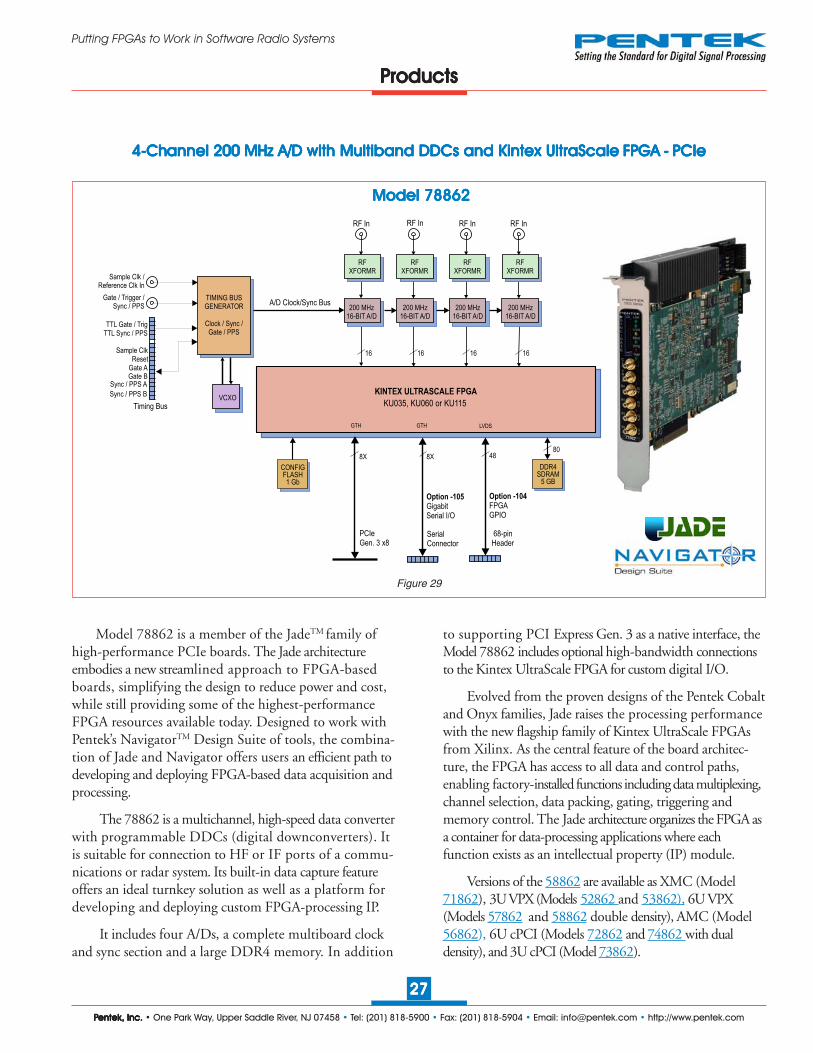
Model 71821 is a member of the JadeTM family ofhigh-performance XMC modules. The Jade architectureembodies a new streamlined approach to FPGA-basedboards, simplifying the design to reduce power and cost,while still providing some of the highest-performanceFPGA resources available today. Designed to work withPentek’s new NavigatorTM Design Suite of tools, thecombination of Jade and Navigator offers users an efficientpath to developing and deploying FPGA-based data acquisitionand processing.
The 71821 is a 3-channel, high-speed data converterwith programmable DDCs. It is suitable for connectionto HF or IF ports of a communications or radar system.Its built-in data capture feature offers an ideal turnkeysolution as well as a platform for developing and deployingcustom FPGA-processing IP.
It includes three A/Ds, a complete multi-board clockand sync section, a large DDR4 memory, three DDCs,one DUC and two D/As. In addition to supporting
PCI Express Gen. 3 as a native interface, the Model 71821includes optional high-bandwidth connections to theKintex UltraScale FPGA for custom digital I/O.
The 71821 factory-installed functions include threeA/D acquisition and a waveform playback IP module forsimplifying data capture and playback, and data transferbetween the board and a host computer. Additional IPincludes: three powerful, programmable DDC IP cores; anIP module for DDR4 SDRAM memory; a controller for alldata clocking and synchronization functions; two test signalgenerators; a programmable interpolator, and a PCIeinterface. These complete the factory-installed functions andenable the 71821 to operate as a complete turnkey solution formany applications.
Versions of the 71821 are also available as an x8 PCIe half-length board (Model 78821), 3U VPX (Models 52821 and53821), 6U VPX (Models 57821 and 58821 dual density),AMC (Model 56821), 6U cPCI (Models 72821 and74821 dual density), and 3U cPCI (Model 73821).
PPPPProductsroductsroductsroductsroducts
PPPPPentek, Inc.entek, Inc.entek, Inc.entek, Inc.entek, Inc. • One Park Way, Upper Saddle River, NJ 07458 • Tel: (201) 818-5900 • Fax: (201) 818-5904 • Email: [email protected] • http://www.pentek.com
2727272727
Putting FPGAs to Work in Software Radio Systems
PPPPProductsroductsroductsroductsroducts
Model 78862 Model 78862 Model 78862 Model 78862 Model 78862
44444-----ChChChChChannelannelannelannelannel 200 MHz 200 MHz 200 MHz 200 MHz 200 MHz A/DA/DA/DA/DA/D with Multiband DDCs and Kintex UltraScale with Multiband DDCs and Kintex UltraScale with Multiband DDCs and Kintex UltraScale with Multiband DDCs and Kintex UltraScale with Multiband DDCs and Kintex UltraScale FPGAFPGAFPGAFPGAFPGA ----- PCIePCIePCIePCIePCIe
TIMING BUSGENERATOR
Clock / Sync /Gate / PPS
VCXO
200 MHz16-BIT A/D
RF In
RFXFORMR
RF In
RFXFORMR
KINTEX ULTRASCALE FPGA
KU035, KU060 or KU115
TTL Gate / TrigTTL Sync / PPS
Sample ClkReset
Gate AGate B
Sync / PPS A
Sync / PPS B
Timing Bus
200 MHz16-BIT A/D
Sample Clk /Reference Clk In
A/D Clock/Sync Bus
1616
RF In
RFXFORMR
200 MHz16-BIT A/D
16
RF In
RFXFORMR
200 MHz16-BIT A/D
16
Gate / Trigger /Sync / PPS
48
LVDS
Option -104FPGAGPIO
68-pinHeader
GTH
8X
SerialConnector
GTH
PCIeGen. 3 x8
CONFIGFLASH1 Gb
DDR4SDRAM
5 GB
808X
Option -105GigabitSerial I/O
Figure 29
Model 78862 is a member of the JadeTM family ofhigh-performance PCIe boards. The Jade architectureembodies a new streamlined approach to FPGA-basedboards, simplifying the design to reduce power and cost,while still providing some of the highest-performanceFPGA resources available today. Designed to work withPentek’s NavigatorTM Design Suite of tools, the combina-tion of Jade and Navigator offers users an efficient path todeveloping and deploying FPGA-based data acquisition andprocessing.
The 78862 is a multichannel, high-speed data converterwith programmable DDCs (digital downconverters). Itis suitable for connection to HF or IF ports of a commu-nications or radar system. Its built-in data capture featureoffers an ideal turnkey solution as well as a platform fordeveloping and deploying custom FPGA-processing IP.
It includes four A/Ds, a complete multiboard clockand sync section and a large DDR4 memory. In addition
to supporting PCI Express Gen. 3 as a native interface, theModel 78862 includes optional high-bandwidth connectionsto the Kintex UltraScale FPGA for custom digital I/O.
Evolved from the proven designs of the Pentek Cobaltand Onyx families, Jade raises the processing performancewith the new flagship family of Kintex UltraScale FPGAsfrom Xilinx. As the central feature of the board architec-ture, the FPGA has access to all data and control paths,enabling factory-installed functions including data multiplexing,channel selection, data packing, gating, triggering andmemory control. The Jade architecture organizes the FPGA asa container for data-processing applications where eachfunction exists as an intellectual property (IP) module.
Versions of the 58862 are available as XMC (Model71862), 3U VPX (Models 52862 and 53862), 6U VPX(Models 57862 and 58862 double density), AMC (Model56862), 6U cPCI (Models 72862 and 74862 with dualdensity), and 3U cPCI (Model 73862).

PPPPPentek, Inc.entek, Inc.entek, Inc.entek, Inc.entek, Inc. • One Park Way, Upper Saddle River, NJ 07458 • Tel: (201) 818-5900 • Fax: (201) 818-5904 • Email: [email protected] • http://www.pentek.com
2828282828
Putting FPGAs to Work in Software Radio Systems
1 GHz A/D, 1 GHz D/A, Vir1 GHz A/D, 1 GHz D/A, Vir1 GHz A/D, 1 GHz D/A, Vir1 GHz A/D, 1 GHz D/A, Vir1 GHz A/D, 1 GHz D/A, Virtex-7 FPGAtex-7 FPGAtex-7 FPGAtex-7 FPGAtex-7 FPGA
Model 71730 Model 71730 Model 71730 Model 71730 Model 71730 - - - - - XMCXMCXMCXMCXMC
Figure 30
PPPPProductsroductsroductsroductsroducts
Model 71730XMC
TIMING BUSGENERATOR
Clock / Sync /Gate / PPS D/A Clock/Sync Bus
VCXO
Gate InSync In
A/D Sync Bus
Sample Clk /Reference Clk In
A/D Clock/Sync Bus
16
RFXFORMR
RF Out
RFXFORMR
RF In
RFXFORMR
1 GHz12-BIT A/D
12Gate InSync In
D/A Sync Bus
1 GHz16-BIT D/A
TTLPPS/Gate/Sync
VIRTEX-7 FPGA
VX330T or VX690T
GigabitSerial I/O(option 105)
GTXGTX LVDSGTX
FPGAGPIO(option 104)
PCIeGen. 3 x8
P14PMC
P16XMC
P15XMC
4X4XCONFIGFLASH1 GB
DDR3SDRAM
1 GB
DDR3SDRAM
1 GB
DDR3SDRAM
1 GB
DDR3SDRAM
1 GB
48 32 32 32 32PCIeGen. 3 x8
FPGAConfigBus
GATEXPRESS PCIeCONFIGURATION
MANAGER
Model 71730 is a member of the Onyx family of high-performance XMC modules based on the Xilinx Virtex-7FPGA. A high-speed data converter, it is suitable forconnection to HF or IF ports of a communications orradar system. Its built-in data capture and playback featuresoffer an ideal turnkey solution as well as a platform fordeveloping and deploying custom FPGA processing IP.It includes 1 GHz A/D and D/A converters and fourbanks of memory. In addition to supporting PCIExpress Gen. 3 as a native interface, the Model 71730includes optional general purpose and gigabit serial cardconnectors for application-specific I/O.
The Pentek Onyx architecture features a Virtex-7FPGA. All of the board’s data and control paths areaccessible by the FPGA, enabling factory-installedfunctions including data multiplexing, channel selection,data packing, gating, triggering and memory control. TheOnyx architecture organizes the FPGA as a container fordata processing applications where each function existsas an intellectual property (IP) module.
Each member of the Onyx family is delivered withfactory-installed applications ideally matched to theboard’s analog interfaces. The 71730 factory-installedfunctions include an A/D acquisition and a D/A waveformplayback IP module for simplifying data capture anddata transfer. IP modules for DDR3 SDRAM memories, acontroller for all data clocking and synchronization functions,a test signal generator and a PCIe interface complete thefactory-installed functions and enable the 71730 tooperate without the need to develop any FPGA IP.
The front end accepts an analog HF or IF input on a frontpanel SSMC connector with transformer coupling into a TIADS5400 1 GHz, 12-bit A/D converter. The digital outputsare delivered to the Virtex-7 FPGA for signal processing, etc.
Versions of the 71730 are also available as an x8 PCIehalf-length board (Model 78730), 3U VPX (Models 52730and 53730), 6U VPX (Models 57730 and 58730 dualdensity), AMC (Model 56730), 6U cPCI (Models 72730and 74730 with dual density), and 3U cPCI (Model 73730).
See page 25
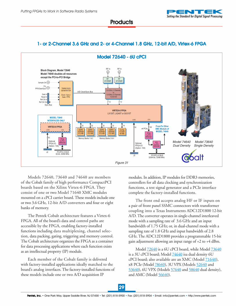
PPPPPentek, Inc.entek, Inc.entek, Inc.entek, Inc.entek, Inc. • One Park Way, Upper Saddle River, NJ 07458 • Tel: (201) 818-5900 • Fax: (201) 818-5904 • Email: [email protected] • http://www.pentek.com
2929292929
Putting FPGAs to Work in Software Radio Systems
Figure 31
PPPPProductsroductsroductsroductsroducts
TIMING BUSGENERATOR
Clock / Sync /Gate / PPS
32
Gate In
Reset In
Sync Bus
Sample Clk
A/D Clock/Sync Bus
16
ConfigFLASH64 MB
32
DDR3SDRAM512 MB
DDR3SDRAM512 MB
3232
DDR3SDRAM512 MB
DDR3SDRAM512 MB
RF In
RFXFORMR
3.6 GHz (1 Channel)or
1.8 GHz (2 Channel)12-bit A/D
12
Memory Banks 1 & 2 Memory Banks 3 & 4
TTLPPS/Gate/Sync
RF In
RFXFORMR
Ref Clk In
Ref Clk Out 12
Block Diagram, Model 72640
Model 74640 doubles all resources
except the PCI-to-PCI Bridge
VIRTEX-6 FPGA
MODEL 73640
INTERFACES ONLY
PCIeto PCI
BRIDGE
40
LVDS GTX
OptionalFPGA I/O(Option -104)
PCI/PCI-X BUS32-bit, 33/66 MHz
J2
PCIeto PCI
BRIDGE
PCIto PCI
BRIDGE
From/To OtherXMC Module ofMODEL 74640
GTX
x4 PCIe
PCI/PCI-X BUS32/64-bit, 33/66 MHz
4X40
LVDS
OptionalFPGA I/O(Option -104)
J3
VIRTEX-6 FPGA
LX130T, LX240T or SX315T
Model 74640Dual Density
Model 73640Single Density
Models 72640, 73640 and 74640 are membersof the Cobalt family of high performance CompactPCIboards based on the Xilinx Virtex-6 FPGA. Theyconsist of one or two Model 71640 XMC modulesmounted on a cPCI carrier board. These models include oneor two 3.6 GHz, 12-bit A/D converters and four or eightbanks of memory.
The Pentek Cobalt architecture features a Virtex-6FPGA. All of the board’s data and control paths areaccessible by the FPGA, enabling factory-installedfunctions including data multiplexing, channel selec-tion, data packing, gating, triggering and memory control.The Cobalt architecture organizes the FPGA as a containerfor data processing applications where each function existsas an intellectual property (IP) module.
Each member of the Cobalt family is deliveredwith factory-installed applications ideally matched to theboard’s analog interfaces. The factory-installed functions ofthese models include one or two A/D acquisition IP
modules. In addition, IP modules for DDR3 memories,controllers for all data clocking and synchronizationfunctions, a test signal generator and a PCIe interfacecomplete the factory-installed functions.
The front end accepts analog HF or IF inputs ona pair of front panel SSMC connectors with transformercoupling into a Texas Instruments ADC12D1800 12-bitA/D. The converter operates in single-channel interleavedmode with a sampling rate of 3.6 GHz and an inputbandwidth of 1.75 GHz; or, in dual-channel mode with asampling rate of 1.8 GHz and input bandwidth of 2.8GHz. The ADC12D1800 provides a programmable 15-bitgain adjustment allowing an input range of +2 to +4 dBm.
Model 72640 is a 6U cPCI board, while Model 73640is a 3U cPCI board; Model 74640 isa dual density 6UcPCI board; also available are an XMC (Model 71640),x8 PCIe (Model 78640), 3U VPX (Models 52640 and53640), 6U VPX (Models 57640 and 58640 dual density),and AMC (Model 56640).
Model 72640 - 6U cPCIModel 72640 - 6U cPCIModel 72640 - 6U cPCIModel 72640 - 6U cPCIModel 72640 - 6U cPCI
1- or 2-1- or 2-1- or 2-1- or 2-1- or 2-Channel 3.6 GHz and 2- or 4-Channel 3.6 GHz and 2- or 4-Channel 3.6 GHz and 2- or 4-Channel 3.6 GHz and 2- or 4-Channel 3.6 GHz and 2- or 4-Channel 1.8 GHz, 12-bit A/D, VirChannel 1.8 GHz, 12-bit A/D, VirChannel 1.8 GHz, 12-bit A/D, VirChannel 1.8 GHz, 12-bit A/D, VirChannel 1.8 GHz, 12-bit A/D, Virtex-6 FPGAtex-6 FPGAtex-6 FPGAtex-6 FPGAtex-6 FPGA

PPPPPentek, Inc.entek, Inc.entek, Inc.entek, Inc.entek, Inc. • One Park Way, Upper Saddle River, NJ 07458 • Tel: (201) 818-5900 • Fax: (201) 818-5904 • Email: [email protected] • http://www.pentek.com
3030303030
Putting FPGAs to Work in Software Radio Systems
PPPPProductsroductsroductsroductsroducts
Figure 32
Model 52851 - 3U VPXModel 52851 - 3U VPXModel 52851 - 3U VPXModel 52851 - 3U VPXModel 52851 - 3U VPX
PPPPProductsroductsroductsroductsroducts
2-2-2-2-2-Channel 500 MHz A/D, with DDCs, DUCs, 2-Channel 500 MHz A/D, with DDCs, DUCs, 2-Channel 500 MHz A/D, with DDCs, DUCs, 2-Channel 500 MHz A/D, with DDCs, DUCs, 2-Channel 500 MHz A/D, with DDCs, DUCs, 2-Channel 800 MHz D/A, Kintex UltraScale FPGAChannel 800 MHz D/A, Kintex UltraScale FPGAChannel 800 MHz D/A, Kintex UltraScale FPGAChannel 800 MHz D/A, Kintex UltraScale FPGAChannel 800 MHz D/A, Kintex UltraScale FPGA
Model 52851 3UVPX Commercial
and rugged
TIMING BUSGENERATOR
Clock / Sync /Gate / PPS
VCXOKINTEX ULTRASCALE FPGA
KU035, KU060 or KU115
TTL Gate / TrigTTL Sync / PPS
Sample ClkReset
Gate AGate B
Sync / PPS A
Sync / PPS B
Timing Bus
Sample Clk /Reference Clk In
Gate / Trigger /Sync / PPS
D/AClock/Sync
Bus
500 MHz12-BIT A/D
RF In
RFXFORMR
RF In
RFXFORMR
500 MHz12-BIT A/D
A/DClock/Sync
Bus800 MHz
16-BIT D/A
RFXFORMR
321616
RF Out
RFXFORMR
RFXFORMR
RF Out
RFXFORMR
800 MHz16-BIT D/A
DIGITALUPCONVERTER
VPX BACKPLANE
CONFIGFLASH1 Gb
DDR4SDRAM
5 GB
80
LVDS
48
Option -104FPGAGPI/O
Option -105GigabitSerial I/O
GTHGTH
8X4X
x4PCIe
VPX-P2 VPX-P1
Model 52851 is a member of the JadeTM family ofhigh-performance 3U VPX boards. The Jade architectureembodies a new stream-lined approach to FPGA-basedboards, simplifying the design to reduce power and cost,while still providing some of the highest-performanceFPGA resources available today. Designed to work withPentek’s new NavigatorTM Design Suite of tools, the combi-nation of Jade and Navigator offers users an efficient pathto developing and deploying FPGA-based data acquisitionand processing.
The 52851 is a 2-channel, high-speed data converterwith programmable DDCs. It is suitable for connectionto HF or IF ports of a communications or radar system.Its built-in data capture feature offers an ideal turnkey solutionas well as a platform for developing and deploying customFPGA-processing IP.
It includes two A/Ds, a complete multiboard clock andsync section, a large DDR4 memory, two DDCs, one DUCand two D/As. In addition to supporting PCI Express
Gen. 3 as a native interface, the Model 52851 includesoptional high-bandwidth connections to the Kintex Ultra-Scale FPGA for custom digital I/O.
The 52851 factory-installed functions include twoA/D acquisition and a waveform playback IP module forsimplifying data capture and playback, and data transferbetween the board and a host computer.
Additional IP includes: a powerful, programmable DDCIP core; an IP module for DDR4 SDRAM memory; acontroller for all data clocking and synchronization func-tions; two test signal generators; a programmable interpola-tor, and a PCIe interface. These complete the factory-installedfunctions and enable the 52851 to operate as a completeturnkey solution for many applications.
Versions of the 52851 are also available as a 3U VPX(Model 53851), 6U VPX (Models 57851 and 58851dual density), XMC module (Model 71851), a PCIe board(Model 78851), AMC (Model 56851), 6U cPCI (Models72851 and 74851dual density), and 3U cPCI (Model 73851).

PPPPPentek, Inc.entek, Inc.entek, Inc.entek, Inc.entek, Inc. • One Park Way, Upper Saddle River, NJ 07458 • Tel: (201) 818-5900 • Fax: (201) 818-5904 • Email: [email protected] • http://www.pentek.com
3131313131
Putting FPGAs to Work in Software Radio Systems
Figure 33
PPPPProductsroductsroductsroductsroducts
Model 71741XMC
TIMING BUSGENERATOR
Clock / Sync /Gate / PPS
Gate In
Reset In
Sync Bus
Sample Clk
A/D Clock/Sync Bus
RF In
RFXFORMR
3.6 GHz (1 Channel)or
1.8 GHz (2 Channel)12-Bit A/D
12
TTLPPS/Gate/Sync
RF In
RFXFORMR
Ref Clk In
Ref Clk Out 12
VIRTEX-7 FPGA
VX330T or VX690T
GTX
PCIeGen. 3 x8
P15XMC
CONFIGFLASH1 GB
DDR3SDRAM
1 GB
DDR3SDRAM
1 GB
DDR3SDRAM
1 GB
DDR3SDRAM
1 GB
32 32 32 32PCIeGen. 3 x8
FPGAConfigBus
GATEXPRESS PCIeCONFIGURATION
MANAGER
GigabitSerial I/O(option 105)
GTXGTX LVDS
FPGAGPIO(option 104)
P14PMC
P16XMC
4X4X 48
Model 71741 is a member of the Onyx family ofhigh-performance XMC modules based on the XilinxVirtex-7 FPGA. A high-speed data converter with aprogrammable digital downconverter, it is suitable forconnection to HF or IF ports of a communications or radarsystem. Its built-in data capture features offer an idealturnkey solution. It includes a 3.6 GHz, 12-bit A/Dconverter and four banks of memory. In addition to support-ing PCI Express Gen. 3 as a native interface, Model 71741includes an optional connection to the Virtex-7 FPGA forcustom I/O.
The Pentek Onyx architecture features a Virtex-7FPGA. All of the board’s data and control paths areaccessible by the FPGA, enabling factory-installedfunctions including data multiplexing, channel selection,data packing, gating, triggering and memory control. TheOnyx architecture organizes the FPGA as a container fordata processing applications where each function existsas an intellectual property (IP) module.
The 71741 factory-installed functions include an A/D acquisition IP module and a programmable digitaldownconverter.
The DDC core supports a single-channel mode,accepting data samples from the A/D at the full 3.6 GHzrate. Additionally, a dual-channel mode supports the A/D’s1.8 GHz two-channel operation. In dual-channel mode, eachDDC has an independent 32-bit tuning frequency settingthat ranges from DC to ƒs,. In single-channel mode, decimationcan be programmed to 8x, 16x or 32x. In dual-channel mode,both channels share the same decimation rate, programmableto 4x, 8x or 16x. See the dataflow diagram of the 71641 onthe previous page for more detail.
Versions of the 71741 are also available as an x8 PCIehalf-length board (Model 78741), 3U VPX (Models 52741and 53741), 6U VPX (Models 57741 and 58741 (dualdensity), AMC (Model 56741), 6U cPCI (Models 72741and 74721 with dual density), and 3U cPCI (Model 73741).
See page 25
Model 71741 - XMCModel 71741 - XMCModel 71741 - XMCModel 71741 - XMCModel 71741 - XMC
1-1-1-1-1-Channel 3.6 GHz or 2-Channel 3.6 GHz or 2-Channel 3.6 GHz or 2-Channel 3.6 GHz or 2-Channel 3.6 GHz or 2-Channel 1.8 GHz, 12-bit A/D, WChannel 1.8 GHz, 12-bit A/D, WChannel 1.8 GHz, 12-bit A/D, WChannel 1.8 GHz, 12-bit A/D, WChannel 1.8 GHz, 12-bit A/D, Wideband DDC, Virideband DDC, Virideband DDC, Virideband DDC, Virideband DDC, Virtex-7 FPGAtex-7 FPGAtex-7 FPGAtex-7 FPGAtex-7 FPGA

PPPPPentek, Inc.entek, Inc.entek, Inc.entek, Inc.entek, Inc. • One Park Way, Upper Saddle River, NJ 07458 • Tel: (201) 818-5900 • Fax: (201) 818-5904 • Email: [email protected] • http://www.pentek.com
3232323232
Putting FPGAs to Work in Software Radio Systems
PPPPProductsroductsroductsroductsroducts
Model 78841 - PCIeModel 78841 - PCIeModel 78841 - PCIeModel 78841 - PCIeModel 78841 - PCIe
1-1-1-1-1-Channel 3.6 GHz or 2-Channel 3.6 GHz or 2-Channel 3.6 GHz or 2-Channel 3.6 GHz or 2-Channel 3.6 GHz or 2-Channel 1.8 GHz, 12-bit A/D, WChannel 1.8 GHz, 12-bit A/D, WChannel 1.8 GHz, 12-bit A/D, WChannel 1.8 GHz, 12-bit A/D, WChannel 1.8 GHz, 12-bit A/D, Wideband DDC, Kintex UltraScale FPGAideband DDC, Kintex UltraScale FPGAideband DDC, Kintex UltraScale FPGAideband DDC, Kintex UltraScale FPGAideband DDC, Kintex UltraScale FPGA
Figure 34
KINTEX ULTRASCALE FPGA
KU035, KU060 or KU115
A/D Clock/Sync Bus
48
LVDS
GPIO
Option -104FPGA
68-pinHeader
GTH
4X
SerialConnector
GTH
PCIeGen. 3 x8
CONFIGFLASH1 GB
DDR4SDRAM
5 GB
808X
Serial I/O
Option -105Gigabit
TIMING BUSGENERATOR
Clock / Sync /Gate / PPS
Gate In
Reset In
Sync Bus
Sample Clk
TTLPPS/Gate/Sync
Ref Clk In
Ref Clk Out
RF In
RFXFORMR
3.6 GHz (1 Channel)or
1.8 GHz (2 Channel)12-Bit A/D
12
RF In
RFXFORMR
12
Model 78841x8 PCIe
Model 78841 is a member of the JadeTM family of high-performance PCIe boards. The Jade architecture embodies anew stream-lined approach to FPGA-based boards,simplifying the design to reduce power and cost, while stillproviding some of the highest-performance FPGA resourcesavailable today. Designed to work with Pentek’s newNavigatorTM Design Suite of tools, the combination ofJade and Navigator offers users an efficient path todeveloping and deploying FPGA-based data acquisitionand processing.
The 78841 is a high-speed data converter with program-mable DDCs). It is suitable for connection to HF or IFports of a communications or radar system. Its built-indata capture feature offers an ideal turnkey solution as wellas a platform for developing and deploying custom FPGA-processing IP.
It includes a 3.6 GHz, 12-bit A/D converter and a largeDDR4 memory. In addition to supporting PCI Express
Gen. 3 as a native interface, Model 78841 includes optionalhigh-bandwidth connections to the Kintex UltraScale FPGAfor custom digital I/O.
Each member of the Jade family is delivered withfactory-installed applications ideally matched to the board’sanalog interfaces. The 78841 factory-installed functionsinclude an A/D acquisition IP module and a program-mable digital downconverter. In addition, IP modules forDDR4 SDRAM memories, a controller for all dataclocking and synchronization functions, a test signalgenerator and a PCIe interface complete the factory-installed functions and enable the 78841 to operate asa complete turnkey solution, without the need to developany FPGA IP.
Versions of the 78841 are also available as an XMCmodule (Model 71841), 3U VPX (Models 52841 and53841), 6U VPX (Models 57841 and 58841 with dualdensity), AMC (Model 56841), 6U cPCI (Models 72841and 74841 with dual density), and 3U cPCI (Model 73841).

PPPPPentek, Inc.entek, Inc.entek, Inc.entek, Inc.entek, Inc. • One Park Way, Upper Saddle River, NJ 07458 • Tel: (201) 818-5900 • Fax: (201) 818-5904 • Email: [email protected] • http://www.pentek.com
3333333333
Putting FPGAs to Work in Software Radio Systems
Figure 35
Model 52650 3UVPX Commercial
and Rugged
PPPPProductsroductsroductsroductsroducts
D/AClock/Sync
Bus
VCXO
500 MHz12-BIT A/D
RF In
RFXFORMR
RF In
RFXFORMR
16
QDRII+SRAM8 MB
TTL Gate / Trig
TTL Sync / PPS
Sample Clk
Reset
Gate A/D
Gate D/A
Sync / PPS A/D
Sync / PPS D/A
Timing Bus
500 MHz12-BIT A/D
Sample Clk /Reference Clk In A/D
Clock/SyncBus 800 MHz
16-BIT D/A
RFXFORMR
321616
RF Out
RFXFORMR
16 16
ConfigFLASH64 MB
16
QDRII+SRAM8 MB
16
RFXFORMR
RF Out
RFXFORMR
800 MHz16-BIT D/A
DIGITALUPCONVERTER
DDR3SDRAM512 MB
DDR3SDRAM512 MB
QDRII+ option 150
16
QDRII+SRAM8 MB
1616
QDRII+SRAM8 MB
16
DDR3SDRAM512 MB
DDR3SDRAM512 MB
Memory Banks 1 & 2 Memory Banks 3 & 4
DDR3 option 155
QDRII+ option 160
DDR3 option 165
TTLPPS/Gate/Sync
TIMING BUSGENERATOR
Clock / Sync /Gate / PPS
LVDS
40
FPGAI/O
Option -104
VPX BACKPLANE
VPX-P2 VPX-P1
VIRTEX-6 FPGA
LX130T, LX240T or SX315T
GTXGTXGTX
GigabitSerial I/O
Option -105
4X4X 4X
x4PCIe
Model 52650 is a member of the Cobalt family ofhigh performance 3U VPX boards based on the XilinxVirtex-6 FPGA. A two-channel, high-speed dataconverter, it is suitable for connection to HF or IF portsof a communications or radar system. Its built-in datacapture and playback features offer an ideal turnkeysolution as well as a platform for developing and deployingcustom FPGA processing IP. The 52650 includes two500 MHz 12-bit A/Ds, one DUC, two 800 MHz 16-bitD/As and four banks of memory. It features built-insupport for PCI Express over the 3U VPX backplane.
The Pentek Cobalt architecture features a Virtex-6FPGA. All of the board’s data and control paths are acces-sible by the FPGA, enabling factory-installed functionsincluding data multiplexing, channel selection, data packing,gating, triggering and memory control. The Cobalt architec-ture organizes the FPGA as a container for data process-ing applications where each function exists as an intellec-tual property (IP) module.
Each member of the Cobalt family is deliveredwith factory-installed applications ideally matched to theboard’s analog interfaces. The 52650 factory-installedfunctions include an A/D acquisition and a D/A waveformplayback IP module. In addition, IP modules for eitherDDR3 or QDRII+ memories, a controller for all dataclocking and synchronization functions, a test signalgenerator and a PCIe interface complete the factory-installed functions.
Multiple 52650’s can be driven from the LVPECL busmaster, supporting synchronous sampling and sync functionsacross all connected boards. The architecture supports up tofour memory banks which can be configured with allQDRII+ SRAM, DDR3 SDRAM, or as combinations.
Versions of the 52650 are also available as a 3U VPX(Model 53650), 6U VPX (Models 57650 and 58650dual density), XMC module (Model 71650), an x8 PCIeboard (Model 78650), AMC (Model 56650), 6U cPCI (Models72650 and 74650 dual density), and 3U cPCI (Model 73650).
This Model is alsoavailable with 400 MHz,
14-bit A/Ds
2-2-2-2-2-Channel 500 MHz A/D, DUC, 2-Channel 500 MHz A/D, DUC, 2-Channel 500 MHz A/D, DUC, 2-Channel 500 MHz A/D, DUC, 2-Channel 500 MHz A/D, DUC, 2-Channel 800 MHz D/A, VirChannel 800 MHz D/A, VirChannel 800 MHz D/A, VirChannel 800 MHz D/A, VirChannel 800 MHz D/A, Virtex-6 FPGAtex-6 FPGAtex-6 FPGAtex-6 FPGAtex-6 FPGA
Model 52650 Model 52650 Model 52650 Model 52650 Model 52650 - - - - - 3U VPX3U VPX3U VPX3U VPX3U VPX

PPPPPentek, Inc.entek, Inc.entek, Inc.entek, Inc.entek, Inc. • One Park Way, Upper Saddle River, NJ 07458 • Tel: (201) 818-5900 • Fax: (201) 818-5904 • Email: [email protected] • http://www.pentek.com
3434343434
Putting FPGAs to Work in Software Radio Systems
PPPPProductsroductsroductsroductsroducts
44444----- or 8- or 8- or 8- or 8- or 8-ChChChChChannelannelannelannelannel 200 MHz 200 MHz 200 MHz 200 MHz 200 MHz A/DA/DA/DA/DA/D with DDCs and Kintex UltraScale with DDCs and Kintex UltraScale with DDCs and Kintex UltraScale with DDCs and Kintex UltraScale with DDCs and Kintex UltraScale FPGAFPGAFPGAFPGAFPGA ----- cPCIcPCIcPCIcPCIcPCI
Models 72861, 73861 & 74861 Models 72861, 73861 & 74861 Models 72861, 73861 & 74861 Models 72861, 73861 & 74861 Models 72861, 73861 & 74861
Figure 36
Model 74861 Model 73861
TIMING BUSGENERATOR
Clock / Sync /Gate / PPS
VCXO
200 MHz16-BIT A/D
RF In
RFXFORMR
RF In
RFXFORMR
KINTEX ULTRASCALE FPGA
KU035, KU060 or KU115
TTL Gate / TrigTTL Sync / PPS
Sample ClkReset
Gate AGate B
Sync / PPS A
Sync / PPS B
Timing Bus
200 MHz16-BIT A/D
Sample Clk /Reference Clk In
A/D Clock/Sync Bus
1616
RF In
RFXFORMR
200 MHz16-BIT A/D
16
RF In
RFXFORMR
200 MHz16-BIT A/D
16
Gate / Trigger /Sync / PPS
CONFIGFLASH1 Gb
DDR4SDRAM
5 GB
80
KINTEX ULTRASCALE FPGA
MODEL 73861
INTERFACES ONLY
PCIeto PCI
BRIDGE
40
LVDS GTX
PCI/PCI-X BUS32-bit, 33/66 MHz
J2
PCIeto PCI
BRIDGE
PCIto PCI
BRIDGE
From/To OtherXMC Module ofMODEL 74861
GTH
PCI/PCI-X BUS32/64-bit, 33/66 MHz
4X40
LVDS
Option -104FPGAGPIO
Option -104FPGAGPIO
J3
Block Diagram, Model 72861
Model 74861 doubles all resources
except the PCI-to-PCI Bridge
Models 72861, 73861 and 74861 are members ofthe JadeTM family of high-performance CompactPCI (cPCI)boards. The Jade architecture embodies a new stream-lined approach to FPGA-based boards, simplifying thedesign to reduce power and cost, while still providing someof the highest-performance FPGA resources available today.Designed to work with Pentek’s NavigatorTM DesignSuite of tools, the combination of Jade and Navigatoroffers users an efficient path to developing and deployingFPGA-based data acquisition and processing.
These models consist of one or two Model 71861XMC modules mounted on a cPCI carrier board. Model72861 is a 6U board while Model 73861 is a 3U board;both have one Model 71861 module. Model 74861 isequipped with two XMC modules rather than one.
They include four or eight A/Ds, complete multi-board clock and sync sections, and a large DDR4 memory.
Evolved from the proven designs of the Pentek Cobaltand Onyx families, Jade raises the processing performancewith the new flagship family of Kintex UltraScale FPGAsfrom Xilinx. As the central feature of the board architec-ture, the FPGA has access to all data and control paths,enabling factory-installed functions including data multiplex-ing, channel selection, data packing, gating, triggeringand memory control. The Jade architecture organizes theFPGA as a container for data-processing applications whereeach function exists as an intellectual property (IP) module.
Each member of the Jade family is delivered with factory-installed applications ideally matched to the board’sanalog interfaces.
Versions of these models are also available as XMC(Model 71861), x8 PCIe (Model 78861), 3U VPX (Models52861 and 53861), 6U VPX (Models 57861 and 58861dual density), and AMC (Model 56861).

PPPPPentek, Inc.entek, Inc.entek, Inc.entek, Inc.entek, Inc. • One Park Way, Upper Saddle River, NJ 07458 • Tel: (201) 818-5900 • Fax: (201) 818-5904 • Email: [email protected] • http://www.pentek.com
3535353535
Putting FPGAs to Work in Software Radio Systems
Figure 37
PPPPProductsroductsroductsroductsroducts
Model 56751AMC
VIRTEX-7 FPGA
VX330T or VX690T
D/AClock/Sync
Bus
VCXO
500 MHz12-BIT A/D
RF In
RFXFORMR
RF In
RFXFORMR
TTL Gate / Trig
TTL Sync / PPS
Sample Clk
Reset
Gate A/D
Gate D/A
Sync / PPS A/D
Sync / PPS D/A
Timing Bus
500 MHz12-BIT A/D
Sample Clk /Reference Clk In A/D
Clock/SyncBus 800 MHz
16-BIT D/A
RFXFORMR
321616
RF Out
RFXFORMR
RFXFORMR
RF Out
RFXFORMR
800 MHz16-BIT D/A
DIGITALUPCONVERTER
TTLPPS/Gate/Sync
TIMING BUSGENERATOR
Clock / Sync /Gate / PPS
LVDSGTX
FPGAGPIO(option 104)
PCIeGen. 2 x8
CONFIGFLASH1 GB
DDR3SDRAM
1 GB
DDR3SDRAM
1 GB
DDR3SDRAM
1 GB
DDR3SDRAM
1 GB
48 32 32 32 32PCIeGen. 2 x8
FPGAConfigBus
GATEXPRESS PCIeCONFIGURATION
MANAGER
FrontPanel
FrontPanel
Ports 4 to 11
IPMICONTROLLER
RS-232
AMC
Model 56751 is a member of the Onyx family ofhigh performance AMC modules based on the XilinxVirtex-7 FPGA. A multichannel, high-speed data converterwith a programmable DDC, it is suitable for connection toHF or IF ports of a communications or radar system. Itsbuilt-in data capture and playback features offer an idealturnkey solution as well as a platform for developing anddeploying custom FPGA processing IP. It includes two A/Ds,two D/As and four banks of memory. In addition tosupporting PCI Express Gen. 2 as a native interface, theModel 56751 includes a general-purpose front-panelconnector for application-specific I/O.
The Pentek Onyx architecture features a Virtex-7FPGA. All of the board’s data and control paths areaccessible by the FPGA, enabling factory-installedfunctions including data multiplexing, channel selection,data packing, gating, triggering and memory control. TheOnyx architecture organizes the FPGA as a container fordata processing applications where each function existsas an intellectual property (IP) module.
Each member of the Onyx family is delivered withfactory-installed applications ideally matched to the board’sanalog interfaces. The 56751 factory-installed functionsinclude two A/D acquisition and a D/A waveform playbackIP modules. Each of the two acquisition IP modulescontains a powerful, programmable DDC IP core. Thewaveform playback IP module contains an interpola-tion IP core, ideal for matching playback rates to the dataand decimation rates of the acquisition modules. IP modulesfor DDR3 memories, a controller for all data clocking andsynchronization functions, a test signal generator, and aPCIe interface complete the factory-installed functionsand enable the 56751 to operate as a turnkey solution,See the block diagram on the previous page for more detail.
Versions of the 56751 are also available as an XMCmodule (Model 71751), x8 PCIe board (Model 78751),3U VPX (Models 52751 and 53751), 6U VPX (Models57751 and 58751 dual density), 6U cPCI (Models 72751and 74751 dual density), and 3U cPCI (Model 73751).
See page 25
Model 56751 - AMCModel 56751 - AMCModel 56751 - AMCModel 56751 - AMCModel 56751 - AMC
2-2-2-2-2-Channel 500 MHz A/D, with DDCs, DUCs, 2-Channel 500 MHz A/D, with DDCs, DUCs, 2-Channel 500 MHz A/D, with DDCs, DUCs, 2-Channel 500 MHz A/D, with DDCs, DUCs, 2-Channel 500 MHz A/D, with DDCs, DUCs, 2-Channel 800 MHz D/A, VirChannel 800 MHz D/A, VirChannel 800 MHz D/A, VirChannel 800 MHz D/A, VirChannel 800 MHz D/A, Virtex-7 FPGAtex-7 FPGAtex-7 FPGAtex-7 FPGAtex-7 FPGA

PPPPPentek, Inc.entek, Inc.entek, Inc.entek, Inc.entek, Inc. • One Park Way, Upper Saddle River, NJ 07458 • Tel: (201) 818-5900 • Fax: (201) 818-5904 • Email: [email protected] • http://www.pentek.com
3636363636
Putting FPGAs to Work in Software Radio Systems
PPPPProductsroductsroductsroductsroducts
Figure 38
Model 52851 - 3U VPXModel 52851 - 3U VPXModel 52851 - 3U VPXModel 52851 - 3U VPXModel 52851 - 3U VPX
PPPPProductsroductsroductsroductsroducts
2-2-2-2-2-Channel 500 MHz A/D, with DDCs, DUCs, 2-Channel 500 MHz A/D, with DDCs, DUCs, 2-Channel 500 MHz A/D, with DDCs, DUCs, 2-Channel 500 MHz A/D, with DDCs, DUCs, 2-Channel 500 MHz A/D, with DDCs, DUCs, 2-Channel 800 MHz D/A, Kintex UltraScale FPGAChannel 800 MHz D/A, Kintex UltraScale FPGAChannel 800 MHz D/A, Kintex UltraScale FPGAChannel 800 MHz D/A, Kintex UltraScale FPGAChannel 800 MHz D/A, Kintex UltraScale FPGA
Model 52851 3UVPX Commercial
and Rugged
Model 52851 is a member of the JadeTM family ofhigh-performance 3U VPX boards. The Jade architectureembodies a new stream-lined approach to FPGA-basedboards, simplifying the design to reduce power and cost,while still providing some of the highest-performanceFPGA resources available today. Designed to work withPentek’s new NavigatorTM Design Suite of tools, the combi-nation of Jade and Navigator offers users an efficient pathto developing and deploying FPGA-based data acquisitionand processing.
The 52851 is a 2-channel, high-speed data converterwith programmable DDCs. It is suitable for connectionto HF or IF ports of a communications or radar system.Its built-in data capture feature offers an ideal turnkey solutionas well as a platform for developing and deploying customFPGA-processing IP.
It includes two A/Ds, a complete multiboard clock andsync section, a large DDR4 memory, two DDCs, one DUCand two D/As. In addition to supporting PCI Express
Gen. 3 as a native interface, the Model 52851 includesoptional high-bandwidth connections to the Kintex Ultra-Scale FPGA for custom digital I/O.
The 52851 factory-installed functions include twoA/D acquisition and a waveform playback IP module forsimplifying data capture and playback, and data transferbetween the board and a host computer.
Additional IP includes: a powerful, programmable DDCIP core; an IP module for DDR4 SDRAM memory; acontroller for all data clocking and synchronization func-tions; two test signal generators; a programmable interpola-tor, and a PCIe interface. These complete the factory-installedfunctions and enable the 52851 to operate as a completeturnkey solution for many applications.
Versions of the 52851 are also available as a 3U VPX(Model 53851), 6U VPX (Models 57851 and 58851dual density), XMC module (Model 71851), a PCIe board(Model 78851), AMC (Model 56851), 6U cPCI (Models72851 and 74851dual density), and 3U cPCI (Model 73851).

PPPPPentek, Inc.entek, Inc.entek, Inc.entek, Inc.entek, Inc. • One Park Way, Upper Saddle River, NJ 07458 • Tel: (201) 818-5900 • Fax: (201) 818-5904 • Email: [email protected] • http://www.pentek.com
3737373737
Putting FPGAs to Work in Software Radio Systems
PPPPProductsroductsroductsroductsroducts
Kintex UltraScaleKintex UltraScaleKintex UltraScaleKintex UltraScaleKintex UltraScale FPGAFPGAFPGAFPGAFPGA Coprocessor Coprocessor Coprocessor Coprocessor Coprocessor----- 3U VPX3U VPX3U VPX3U VPX3U VPX
Model 53800Model 53800Model 53800Model 53800Model 53800
Option -105Gigabit Serial I/O
PCIeGen. 3 x8
4X
GigabitSerial
4X
GigabitSerial
4X
GigabitSerial
4X
GigabitSerial
VPX–P1
CROSSBARSWITCH
KINTEX ULTRASCALE FPGAKU035, KU060 or KU115
LVDS
48
Option -104FPGAI/O
VPX-P2
CONFIGFLASH1 Gb
VPX BACKPLANE
DDR4SDRAM
5 GB
80
PROGRAMMABLE CLOCKING
GENERATOR
VCXO
FPGA Clocks
LVDS
Front PanelFPGAGPIO
76
Figure 39
Model 52800 Commercial (left)and Rugged version
Model 52800 is a member of the JadeTM family ofhigh-performance 3U VPX boards. The Jade architectureembodies a new streamlined approach to FPGA basedboards, simplifying the design to reduce power and cost,while still providing some of the highest performance FPGAresources available today.
Designed to work with Pentek’s NavigatorTM DesignSuite of tools, the combination of Jade and Navigator offersusers an efficient path to developing and deploying FPGA-based data processing IP.
In addition to supporting PCI Express Gen. 3 as anative interface, the Model 53800 includes optional high-band-width serial and parallel connections to the Kintex UltraScaleFPGA for custom digital I/O.
Evolved from the proven designs of the Pentek Cobaltand Onyx families, Jade raises the processing performancewith the new flagship family of Kintex UltraScale FPGAs
from Xilinx. As the central feature of the board architecture,the FPGA has access to all data and control paths. The Jadearchitecture organizes the FPGA as a container for data-proces-sing applications where each function exists as an intellectualproperty (IP) module.
Each member of the Jade family is delivered with factory-installed applications ideally matched to the board’s inter-faces. The 52800 factory-installed functions include a testsignal generator, a metadata generator, a DDR4 SDRAMcontroller, and DMA engines for moving data on and offthe board.
Versions of the 53800 are also available as an XMC(Model 71800), an x8 PCIe half-length board (Model 58800),another 3U VPX (Model 52800), 6U VPX (Models 57800and 58800 (dual density), AMC (Model 56800), 6U cPCI(Models 72800 and 74800 with dual density), and 3U cPCI(Model 73800).

PPPPPentek, Inc.entek, Inc.entek, Inc.entek, Inc.entek, Inc. • One Park Way, Upper Saddle River, NJ 07458 • Tel: (201) 818-5900 • Fax: (201) 818-5904 • Email: [email protected] • http://www.pentek.com
3838383838
Putting FPGAs to Work in Software Radio Systems
Figure 40
PPPPProductsroductsroductsroductsroducts
Model 587616U VPX
Dual Density
Model 58761 is a member of the Onyx family of high-performance OpenVPX boards based on the Xilinx Virtex-7FPGA. A multichannel, high-speed data converter based on theModel 71760 described previously, it includes factory-installedIP cores to enhance the performance of the 71760 andaddress the requirements of many applications.
The 58761 factory-installed functions include eight A/Dacquisition IP modules. Each of the acquisition IP modulescontains a powerful, programmable DDC IP core. IPmodules for DDR3 memories, controllers for all dataclocking and synchronization functions, test signalgenerators, Aurora gigabit serial interfaces, and a PCIeinterface complete the factory-installed functions.
Each DDC has an independent 32-bit tuningfrequency setting that ranges from DC to ƒs, where ƒs isthe A/D sampling frequency. Each DDC can have itsown unique decimation setting, supporting as many aseight different output bandwidths for the board. Decima-
tions can be programmed from 2 to 65,536 providing awide range to satisfy most applications.
The 58761 also features two complete beamformingsubsystems. Each DDC core contains programmable I &Q phase and gain adjustments followed by a power meterthat continuously measures the individual average poweroutput. The power meters present average power measure-ments for each DDC core output in easy-to-read registers. Athreshold detector automatically sends an interrupt tothe processor if the average power level of any DDCcore falls below or exceeds a programmable threshold.
For larger systems, multiple 58761’s can be chainedtogether via the built-in Xilinx Aurora gigabit serialinterfaces.
Versions of the 58761 are also available as XMC (Model71761), x8 PCIe half-length board (Model 78761), 3U VPX(Models 52761 and 53761), 6U VPX (Model 57761 singledensity), AMC (Model 56761), 6U cPCI (Models 72761and 74761 dual density), and 3U cPCI (Model 73761).
See page 25
LVDS
48
FPGAI/O
Option -104
VPX BACKPLANE
VPX-P3
VIRTEX-7 FPGA
VX330T or VX690T
DDR3SDRAM
1 GB
DDR3SDRAM
1 GB
DDR3SDRAM
1 GB
DDR3SDRAM
1 GB
32 32 32 32
GTXGTXGTX
PCIeGen. 3 x8
4X4X
PCIeGen. 3 x8
CONFIGFLASH1 GB
PCIeGen. 3x8
FPGAConfigBus
GATEXPRESS PCIeCONFIGURATION
MANAGER
VPX-P2VPX-P1
PCIe-to PCIeSWITCH
From/ToOther XMCModule ofModel 58761
AuroraGigabit Serial I/O
Block Diagram, Model 57761.
Model 58761 doubles all resources
except the PCIe-to-PCIe Switch and
provides 24 LVDS pairs from the
2nd FPGA to VPX-P5
Sumtonextboard
Sumfrompriorboard
TIMING BUSGENERATOR
Clock / Sync /Gate / PPS
200 MHz16-BIT A/D
RF In
RFXFORMR
RF In
RFXFORMR
TTL Gate / TrigTTL Sync / PPS
Sample ClkReset
Gate AGate B
Sync / PPS A
Sync / PPS B
Timing Bus
200 MHz16-BIT A/D
Sample Clk /Reference Clk In
A/D Clock/Sync Bus
1616
RF In
RFXFORMR
200 MHz16-BIT A/D
16
RF In
RFXFORMR
200 MHz16-BIT A/D
16
Gate / Trigger /Sync / PPS
VCXO
4-4-4-4-4-Channel 200 MHz 16-bit A/D with Installed IP Cores, VirChannel 200 MHz 16-bit A/D with Installed IP Cores, VirChannel 200 MHz 16-bit A/D with Installed IP Cores, VirChannel 200 MHz 16-bit A/D with Installed IP Cores, VirChannel 200 MHz 16-bit A/D with Installed IP Cores, Virtex-7 FPGAtex-7 FPGAtex-7 FPGAtex-7 FPGAtex-7 FPGA
Model 58761 - 6U VPX, Dual DensityModel 58761 - 6U VPX, Dual DensityModel 58761 - 6U VPX, Dual DensityModel 58761 - 6U VPX, Dual DensityModel 58761 - 6U VPX, Dual Density

PPPPPentek, Inc.entek, Inc.entek, Inc.entek, Inc.entek, Inc. • One Park Way, Upper Saddle River, NJ 07458 • Tel: (201) 818-5900 • Fax: (201) 818-5904 • Email: [email protected] • http://www.pentek.com
3939393939
Putting FPGAs to Work in Software Radio Systems
PPPPProductsroductsroductsroductsroducts
4-4-4-4-4-Channel 200 MHz 16-bit A/D with Installed IP Cores, Kintex Ultrascale FPGAChannel 200 MHz 16-bit A/D with Installed IP Cores, Kintex Ultrascale FPGAChannel 200 MHz 16-bit A/D with Installed IP Cores, Kintex Ultrascale FPGAChannel 200 MHz 16-bit A/D with Installed IP Cores, Kintex Ultrascale FPGAChannel 200 MHz 16-bit A/D with Installed IP Cores, Kintex Ultrascale FPGA
Model 72861 - 6U cPCIModel 72861 - 6U cPCIModel 72861 - 6U cPCIModel 72861 - 6U cPCIModel 72861 - 6U cPCI
Figure 41
Model 74861Dual Density
Model 73861Single Density
Models 72861, 73861 and 74861 are members ofthe JadeTM family of high-performance CompactPCI (cPCI)boards. The Jade architecture embodies a new streamlinedapproach to FPGA-based boards, simplifying the design toreduce power and cost, while still providing some of thehighest-performance FPGA resources available today.Designed to work with Pentek’s new NavigatorTM DesignSuite of tools, the combination of Jade and Navigatoroffers users an efficient path to developing and deployingFPGA-based data acquisition and processing.
These models consist of one or two Model 71861XMC modules mounted on a cPCI carrier board. Model72861 is a 6U board while Model 73861 is a 3U board;both have one Model 71861 module. Model 74861 isequipped with two XMC modules rather than one.
The cPCI models include four or eight A/Ds, completemultiboard clock and sync sections, and large DDR4 memories.Each member of the Jade family is delivered with factory-installedapplications ideally matched to the board’s analog interfaces.
The factory-installed functions include four or eight A/Dacquisition IP modules for simplifying data capture andtransfer.
Each of the acquisition IP modules contains a powerful,programmable DDC IP core; IP modules for DDR4SDRAM memory; controllers for all data clocking andsynchronization functions; test signal generators; and a PCIeinterface. These complete the factory-installed functionsand enable these models to operate as complete turnkeysolutions for many applications, The architecture supports 5or 10 GB banks of DDR4 SDRAM memory. User-installedIP along with the Pentek-supplied DDR4 controller corewithin the FPGA can take advantage of the memory forcustom applications.
Model 72861 is a 6U cPCI board, while Model 73861 is a3U cPCI board; Model 74861 isa dual density 6U cPCI board;also available are an XMC (Model 71861), x8 PCIe (Model78861), 3U VPX (Models 52861 and 53861), 6U VPX (Models57861 and 58861 dual density), and AMC (Model 56861).
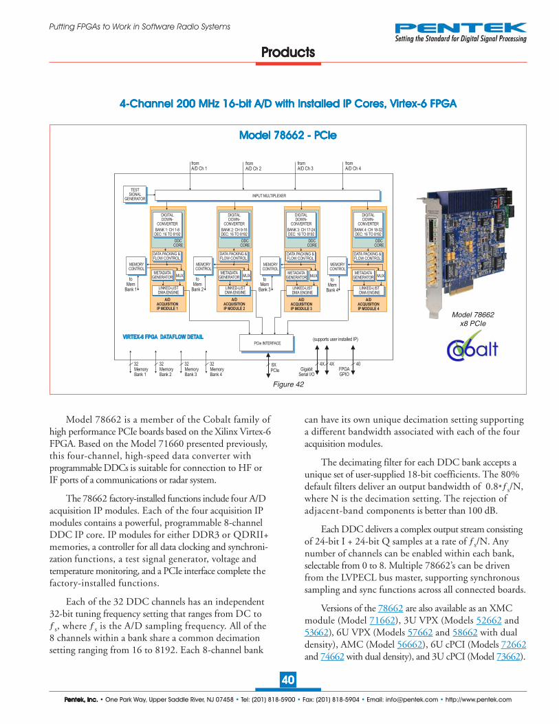
PPPPPentek, Inc.entek, Inc.entek, Inc.entek, Inc.entek, Inc. • One Park Way, Upper Saddle River, NJ 07458 • Tel: (201) 818-5900 • Fax: (201) 818-5904 • Email: [email protected] • http://www.pentek.com
4040404040
Putting FPGAs to Work in Software Radio Systems
Figure 42
fromA/D Ch 1
fromA/D Ch 2
fromA/D Ch 3
fromA/D Ch 4
VIRTEX-6 FPGA DATAFLOW DETAILVIRTEX-6 FPGA DATAFLOW DETAIL
A/DACQUISITIONIP MODULE 1
A/DACQUISITIONIP MODULE 2
A/DACQUISITIONIP MODULE 3
A/DACQUISITIONIP MODULE 4
LINKED-LISTDMA ENGINE
LINKED-LISTDMA ENGINE
METADATAGENERATOR
METADATAGENERATOR
METADATAGENERATOR
METADATAGENERATORto
MemBank 1
MEMORYCONTROL
toMem
Bank 2
MEMORYCONTROL
toMem
Bank 3
toMem
Bank 4
MEMORYCONTROL
MEMORYCONTROL
MUX MUX MUX MUX
DATA PACKING &FLOW CONTROL
DATA PACKING &FLOW CONTROL
DATA PACKING &FLOW CONTROL
DATA PACKING &FLOW CONTROL
INPUT MULTIPLEXER
TESTSIGNAL
GENERATOR
DATA PACKING &FLOW CONTROL
DATA PACKING &FLOW CONTROL
DDCCORE
DIGITALDOWN-
CONVERTER
BANK 1: CH 1-8DEC: 16 TO 8192
.
DDCCORE
DIGITALDOWN-
CONVERTER
BANK 2: CH 9-16DEC: 16 TO 8192
.
DDCCORE
DIGITALDOWN-
CONVERTER
BANK 3: CH 17-24DEC: 16 TO 8192
.
DDCCORE
DIGITALDOWN-
CONVERTER
BANK 4: CH 18-32DEC: 16 TO 8192
.
MemoryBank 4
PCIe INTERFACE
PCIe8X
LINKED-LISTDMA ENGINE
LINKED-LISTDMA ENGINE
GigabitSerial I/O
FPGAGPIO
(supports user installed IP)
4X 4X 4032MemoryBank 3
32MemoryBank 2
32MemoryBank 1
32
PPPPProductsroductsroductsroductsroducts
Model 78662 is a member of the Cobalt family ofhigh performance PCIe boards based on the Xilinx Virtex-6FPGA. Based on the Model 71660 presented previously,this four-channel, high-speed data converter withprogrammable DDCs is suitable for connection to HF orIF ports of a communications or radar system.
The 78662 factory-installed functions include four A/Dacquisition IP modules. Each of the four acquisition IPmodules contains a powerful, programmable 8-channelDDC IP core. IP modules for either DDR3 or QDRII+memories, a controller for all data clocking and synchroni-zation functions, a test signal generator, voltage andtemperature monitoring, and a PCIe interface complete thefactory-installed functions.
Each of the 32 DDC channels has an independent32-bit tuning frequency setting that ranges from DC toƒs, where ƒs is the A/D sampling frequency. All of the8 channels within a bank share a common decimationsetting ranging from 16 to 8192. Each 8-channel bank
can have its own unique decimation setting supportinga different bandwidth associated with each of the fouracquisition modules.
The decimating filter for each DDC bank accepts aunique set of user-supplied 18-bit coefficients. The 80%default filters deliver an output bandwidth of 0.8*ƒs/N,where N is the decimation setting. The rejection ofadjacent-band components is better than 100 dB.
Each DDC delivers a complex output stream consistingof 24-bit I + 24-bit Q samples at a rate of ƒs/N. Anynumber of channels can be enabled within each bank,selectable from 0 to 8. Multiple 78662’s can be drivenfrom the LVPECL bus master, supporting synchronoussampling and sync functions across all connected boards.
Versions of the 78662 are also available as an XMCmodule (Model 71662), 3U VPX (Models 52662 and53662), 6U VPX (Models 57662 and 58662 with dualdensity), AMC (Model 56662), 6U cPCI (Models 72662and 74662 with dual density), and 3U cPCI (Model 73662).
Model 78662x8 PCIe
4-4-4-4-4-Channel 200 MHz 16-bit A/D with Installed IP Cores, VirChannel 200 MHz 16-bit A/D with Installed IP Cores, VirChannel 200 MHz 16-bit A/D with Installed IP Cores, VirChannel 200 MHz 16-bit A/D with Installed IP Cores, VirChannel 200 MHz 16-bit A/D with Installed IP Cores, Virtex-6 FPGAtex-6 FPGAtex-6 FPGAtex-6 FPGAtex-6 FPGA
Model 786Model 786Model 786Model 786Model 7866262626262 - - - - - PCIePCIePCIePCIePCIe

PPPPPentek, Inc.entek, Inc.entek, Inc.entek, Inc.entek, Inc. • One Park Way, Upper Saddle River, NJ 07458 • Tel: (201) 818-5900 • Fax: (201) 818-5904 • Email: [email protected] • http://www.pentek.com
4141414141
Putting FPGAs to Work in Software Radio Systems
Figure 43
SUPERCHANNELENGINE
PACKETGENERATOR
FIFO &LINKED-LISTDMA ENGINE
GEN 2x4 PCIe
INTERFACE
SUPERCHANNELENGINE
SUPERCHANNELENGINE
SUPERCHANNELENGINE
PACKETGENERATOR
PACKETGENERATOR
PACKETGENERATOR
FIFO &LINKED-LISTDMA ENGINE
FIFO &LINKED-LISTDMA ENGINE
FIFO &LINKED-LISTDMA ENGINE
Sample /Ref Clock In
MUX
180 MHz16-BIT A/D
Ch ARF In GSM
CHANNELIZER375 CHANNELS
MUX
MUX
MUX
Ch BRF In
Ch CRF In
Ch DRF In
180 MHzVCXO
CLOCK, SYNC& TRIGGER
GENERATOR
Clock /SyncBus
GSMCHANNELIZER375 CHANNELS
GSMCHANNELIZER175 CHANNELS
GSMCHANNELIZER175 CHANNELS
180 MHz16-BIT A/D
180 MHz16-BIT A/D
180 MHz16-BIT A/D
Gate / Trigger /Sync / PPS VPX BACKPLANE
VPX-P1
4X
x4PCIe
PPPPProductsroductsroductsroductsroducts
Model 52633 3U VPXCommercial and
Rugged
The Model 52663 accepts four analog inputs froman external analog RF tuner, such as the Pentek Model8111, where the GSM RF bands are downconverted toan IF frequency. These IF signals are then digitized byfour A/D converters and routed to four channelizerbanks, which perform digital downconversion of allGSM channels to baseband. Two of the banks handle175 channels for the lower GSM transmit/receive bandsand two more banks handle 375 channels for the upperbands. The DDC channels within each bank are equallyspaced at 200 kHz.
Each DDC output is resampled to a 4x symbol rateof 1.08333 MHz to simplify symbol recovery. Every fourDDC outputs are combined into a frequency-division“super-channel” that allows transmission of all 1100channels across the PCIe Gen. 2 x4 interface. The GSMchannelizer IP core is supported with factory-installedFPGA functions including packet formation, timestamping, four DMA controllers, gating and triggering.
Super-channel packets are formed by appendingenabled super-channel samples sequentially from eachbank. Once complete, a unique super-channel packetheader is inserted at the beginning of each packet foridentification. The header contains a time stamp, asequential packet count, the number of enabled super-channels, the DMA channel identifier, and other information.
The 52663 is ideal for mobile monitoring systemsthat must capture some or all of the 1100 uplink anddownlink signals in both upper and lower GSM bands.This full-global system for mobile communicationsspectrum monitoring targets homeland security, govern-ment and military applications.
Versions of the 52663 are also available as an XMC module (Model 71663), an x8 PCIe half-length board(Model 78663), 3U VPX (Model 53663), 6U VPX(Models 57663 and 58663 with dual density), AMC (Model 56663), 6U cPCI (Models 72663 and 74663 with dual density), and 3U cPCI (Model 73663).
1100-1100-1100-1100-1100-Channel GSM Channelizer with Quad A/D, VirChannel GSM Channelizer with Quad A/D, VirChannel GSM Channelizer with Quad A/D, VirChannel GSM Channelizer with Quad A/D, VirChannel GSM Channelizer with Quad A/D, Virtex-6 FPGAtex-6 FPGAtex-6 FPGAtex-6 FPGAtex-6 FPGA
Model 52Model 52Model 52Model 52Model 52663663663663663 - - - - - 3U VPX3U VPX3U VPX3U VPX3U VPX

PPPPPentek, Inc.entek, Inc.entek, Inc.entek, Inc.entek, Inc. • One Park Way, Upper Saddle River, NJ 07458 • Tel: (201) 818-5900 • Fax: (201) 818-5904 • Email: [email protected] • http://www.pentek.com
4242424242
Putting FPGAs to Work in Software Radio Systems
TIMING BUSGENERATOR
Clock / Sync /Gate / PPS
VCXO
200 MHz16-BIT A/D
RF In
RFXFORMR
RF In
RFXFORMR
KINTEX ULTRASCALE FPGA
KU035, KU060 or KU115
TTL Gate / TrigTTL Sync / PPS
Sample ClkReset
Gate AGate B
Sync / PPS A
Sync / PPS B
Timing Bus
200 MHz16-BIT A/D
Sample Clk /Reference Clk In
A/D Clock/Sync Bus
1616
RF In
RFXFORMR
200 MHz16-BIT A/D
16
RF In
RFXFORMR
200 MHz16-BIT A/D
16
Gate / Trigger /Sync / PPS
CONFIGFLASH1 Gb
DDR4SDRAM
5 GB
80
KINTEX ULTRASCALE FPGA
MODEL 73861
INTERFACES ONLY
PCIeto PCI
BRIDGE
40
LVDS GTX
PCI/PCI-X BUS32-bit, 33/66 MHz
J2
PCIeto PCI
BRIDGE
PCIto PCI
BRIDGE
From/To OtherXMC Module ofMODEL 74861
GTH
PCI/PCI-X BUS32/64-bit, 33/66 MHz
4X40
LVDS
Option -104FPGAGPIO
Option -104FPGAGPIO
J3
Block Diagram, Model 72861
Model 74861 doubles all resources
except the PCI-to-PCI Bridge
PPPPProductsroductsroductsroductsroducts
4-4-4-4-4-Channel 200 MHz 16-bit A/D with Installed IP Cores, Kintex Ultrascale FPGAChannel 200 MHz 16-bit A/D with Installed IP Cores, Kintex Ultrascale FPGAChannel 200 MHz 16-bit A/D with Installed IP Cores, Kintex Ultrascale FPGAChannel 200 MHz 16-bit A/D with Installed IP Cores, Kintex Ultrascale FPGAChannel 200 MHz 16-bit A/D with Installed IP Cores, Kintex Ultrascale FPGA
Model 72861 - 6U cPCIModel 72861 - 6U cPCIModel 72861 - 6U cPCIModel 72861 - 6U cPCIModel 72861 - 6U cPCI
Figure 44
Model 74861Dual Density
Model 73861Single Density
Models 72861, 73861 and 74861 are members ofthe JadeTM family of high-performance CompactPCI (cPCI)boards. The Jade architecture embodies a new streamlinedapproach to FPGA-based boards, simplifying the design toreduce power and cost, while still providing some of thehighest-performance FPGA resources available today.Designed to work with Pentek’s new NavigatorTM DesignSuite of tools, the combination of Jade and Navigatoroffers users an efficient path to developing and deployingFPGA-based data acquisition and processing.
These models consist of one or two Model 71861XMC modules mounted on a cPCI carrier board. Model72861 is a 6U board while Model 73861 is a 3U board;both have one Model 71861 module. Model 74861 isequipped with two XMC modules rather than one.
The cPCI models include four or eight A/Ds, completemultiboard clock and sync sections, and large DDR4 memories.Each member of the Jade family is delivered with factory-installedapplications ideally matched to the board’s analog interfaces.
The factory-installed functions include four or eight A/Dacquisition IP modules for simplifying data capture andtransfer.
Each of the acquisition IP modules contains a powerful,programmable DDC IP core; IP modules for DDR4SDRAM memory; controllers for all data clocking andsynchronization functions; test signal generators; and a PCIeinterface. These complete the factory-installed functionsand enable these models to operate as complete turnkeysolutions for many applications, The architecture supports 5or 10 GB banks of DDR4 SDRAM memory. User-installedIP along with the Pentek-supplied DDR4 controller corewithin the FPGA can take advantage of the memory forcustom applications.
Model 72861 is a 6U cPCI board, while Model 73861 is a3U cPCI board; Model 74861 isa dual density 6U cPCI board;also available are an XMC (Model 71861), x8 PCIe (Model78861), 3U VPX (Models 52861 and 53861), 6U VPX (Models57861 and 58861 dual density), and AMC (Model 56861).

PPPPPentek, Inc.entek, Inc.entek, Inc.entek, Inc.entek, Inc. • One Park Way, Upper Saddle River, NJ 07458 • Tel: (201) 818-5900 • Fax: (201) 818-5904 • Email: [email protected] • http://www.pentek.com
4343434343
Putting FPGAs to Work in Software Radio Systems
Figure 45
Model 576706U VPX
Single Density
Model 57670 is a member of the Cobalt family ofhigh performance 6U OpenVPX boards based on theXilinx Virtex-6 FPGA. This 4-channel, high-speed dataconverter is suitable for connection to transmit HF or IFports of a communications or radar system. Its built-indata playback features offer an ideal turnkey solutionfor demanding transmit applications. It includes fourD/As, four digital upconverters and four banks ofmemory. In addition to supporting PCI Express Gen. 2 asa native interface, the Model 57670 includes a front panelgeneral-purpose connector for application-specific I/O.
The Pentek Cobalt Architecture features a Virtex-6FPGA. All of the board’s data and control paths areaccessible by the FPGA, enabling factory-installed functionsincluding data multiplexing, channel selection, datapacking, gating, triggering and memory control. TheCobalt Architecture organizes the FPGA as a containerfor data processing applications where each functionexists as an intellectual property (IP) module.
Each member of the Cobalt family is delivered withfactory-installed applications ideally matched to the board’sanalog interfaces. The Model 57670 factory-installedfunctions include a sophisticated D/A WaveformPlayback IP module. Four linked-list controllers supportwaveform generation to the four D/As from tables storedin either on-board memory or off-board host memory.
IP modules for DDR3 SDRAM memories, acontroller for all data clocking and synchronizationfunctions, a test signal generator, and a PCIe interfacecomplete the factory-installed functions and enable the57670 to operate as a turnkey solution without the need todevelop FPGA IP.
Versions of the 57670 are also available as XMC(Model 71670), PCIe (Model 78670), 3U VPX (Models52670 and 53670), 6U VPX (Model 58670 dual density),AMC (Model 56670) 6U cPCI (Models 72670 and74670 dual density), and 3U cPCI (Model 73670).
PPPPProductsroductsroductsroductsroducts
VIRTEX-6 FPGA
LX130T, LX240T or SX315T
16
ConfigFLASH64 MB
LVDS GTX
40 8X
FPGAI/O
Option -104
VPX BACKPLANE
VPX-P3
GTXGTX
PCIeGen. 2 x8
4X 4X
VPX-P2VPX-P1
Option -105Gigabit Serial I/O
TIMING BUSGENERATOR
Clock / Sync /Gate / PPS
VCXO
Sample Clk /Reference Clk In
Clock/SyncBus A
RFXFORMR
16-BIT D/A1.25 GHz
DIGITALUPCONVERTER
RF Out
RFXFORMR
RFXFORMR
1.25 GHz16-BIT D/A
DIGITALUPCONVERTER
RF Out
RFXFORMR
RFXFORMR
16-BIT D/A1.25 GHz
DIGITALUPCONVERTER
RF Out
RFXFORMR
RFXFORMR
1.25 GHz16-BIT D/A
DIGITALUPCONVERTER
RF Out
RFXFORMR
16 16
Gate InSync In
�Sync Bus A
Gate InSync In
�Sync Bus B
Trigger In
Clock/SyncBus B
3232
DDR3SDRAM512 MB
DDR3SDRAM512 MB
3232
DDR3SDRAM512 MB
DDR3SDRAM512 MB
Memory Banks 1 & 2 Memory Banks 3 & 4
4-4-4-4-4-Channel 1.25 GHz D/A with DUC, VirChannel 1.25 GHz D/A with DUC, VirChannel 1.25 GHz D/A with DUC, VirChannel 1.25 GHz D/A with DUC, VirChannel 1.25 GHz D/A with DUC, Virtex-6 FPGAtex-6 FPGAtex-6 FPGAtex-6 FPGAtex-6 FPGA
Model 5Model 5Model 5Model 5Model 57670 - 7670 - 7670 - 7670 - 7670 - 6U VPX6U VPX6U VPX6U VPX6U VPX, Single Density, Single Density, Single Density, Single Density, Single Density

PPPPPentek, Inc.entek, Inc.entek, Inc.entek, Inc.entek, Inc. • One Park Way, Upper Saddle River, NJ 07458 • Tel: (201) 818-5900 • Fax: (201) 818-5904 • Email: [email protected] • http://www.pentek.com
4444444444
Putting FPGAs to Work in Software Radio Systems
PPPPProductsroductsroductsroductsroducts
Model 58132
KINTEX ULTRASCALE FPGA
KU060 or KU115
CONFIGFLASH1 Gb
VPX BACKPLANE
16
LVDS GTH
48 8X
Option -104FPGA
I/O
VPX-P3
GTHGTH
PCIeGen. 2 x8
4X4X
PCIeGen. 3 x8
VPX-P2VPX-P1
PCIe-to PCIeSWITCH
From/ToOther XMCModule ofModel 58132
Option -105Gigabit Serial I/O
DDR4SDRAM
5 GB
80
Block Diagram, Model 57132.
Model 58132 doubles all
resources except the
PCIe-to-PCIe Switch and
provides 24 LVDS pairs
from the 2nd FPGA to VPX-P5
250 MHz16-BIT A/D
RF In
RFXFORMR
RF In
RFXFORMR
A/DClock/Sync
Bus
1616
RF In
RFXFORMR
16
RF In
RFXFORMR
16
RF In
RFXFORMR
RF In
RFXFORMR
1616
RF In
RFXFORMR
16
RF In
RFXFORMR
16
TIMING BUSGENERATOR
Clock / Sync /Gate / PPS
VCXO
TTL Gate / TrigTTL Sync / PPS
Sample Clk
Reset
Gate
Sync / PPS
Timing Bus
Sample Clk /Reference Clk In
A/DClock/Sync
BusGate / Trigger /Sync / PPS 250 MHz
16-BIT A/D250 MHz
16-BIT A/D250 MHz
16-BIT A/D250 MHz
16-BIT A/D250 MHz
16-BIT A/D250 MHz
16-BIT A/D250 MHz
16-BIT A/D
88888----- or 16- or 16- or 16- or 16- or 16-ChChChChChannelannelannelannelannel 2 2 2 2 2555550 MHz0 MHz0 MHz0 MHz0 MHz A/DA/DA/DA/DA/D with Multiband DDCs and Kintex UltraScale with Multiband DDCs and Kintex UltraScale with Multiband DDCs and Kintex UltraScale with Multiband DDCs and Kintex UltraScale with Multiband DDCs and Kintex UltraScale FPGAFPGAFPGAFPGAFPGA ----- 6U VPX6U VPX6U VPX6U VPX6U VPX
Model 58132Model 58132Model 58132Model 58132Model 58132
Figure 46
Models 57132 and 58132 are members of the JadeTM
family of high-performance 6U VPX boards. The Jadearchitecture embodies a new streamlined approach to FPGA-based boards, simplifying the design to reduce power andcost, while still providing some of the highest-performanceFPGA resources available today. Designed to work withPentek’s NavigatorTM Design Suite of tools, the combina-tion of Jade and Navigator offers users an efficient path todeveloping and deploying FPGA-based data acquisition andprocessing.
These models consist of one or two Model 71132XMC modules mounted on a VPX carrier board. Model57132 is a 6U board with one Model 71132 modulewhile the Model 58132 is a 6U board with two XMCmodules rather than one.
They include four or eight A/Ds, complete multiboardclock and sync sections, and a large DDR4 memory. Inaddition to supporting PCI Express Gen. 3 as a native
interface, these models include optional high-bandwidthconnections to the Kintex UltraScale FPGA for custom digitalI/O.
Evolved from the proven designs of the Pentek Cobaltand Onyx families, Jade raises the processing performancewith the new flagship family of Kintex UltraScale FPGAsfrom Xilinx. As the central feature of the board architec-ture, the FPGA has access to all data and control paths,enabling factory-installed functions including data multiplex-ing, channel selection, data packing, gating, triggeringand memory control. The Jade architecture organizes theFPGA as a container for data-processing applications whereeach function exists as an intellectual property (IP) module.
Versions of the 58132 are also available as an XMC (Model71132), an x8 PCIe half-length board (Model 58132), 3UVPX (Models 52132 and 53132), 6U VPX (Model 57132single density), AMC (Model 56132), 6U cPCI (Models72132 and 74132 dual density), and 3U cPCI (Model 73132).

PPPPPentek, Inc.entek, Inc.entek, Inc.entek, Inc.entek, Inc. • One Park Way, Upper Saddle River, NJ 07458 • Tel: (201) 818-5900 • Fax: (201) 818-5904 • Email: [email protected] • http://www.pentek.com
4545454545
Putting FPGAs to Work in Software Radio Systems
Figure 47
PPPPProductsroductsroductsroductsroducts
Model 71771XMC
TIMING BUSGENERATOR
Clock / Sync /Gate / PPS
VCXO
Sample Clk /Reference Clk In
Clock/SyncBus A
RFXFORMR
16-BIT D/A1.25 GHz
DIGITALUPCONVERTER
RF Out
RFXFORMR
RFXFORMR
1.25 GHz16-BIT D/A
DIGITALUPCONVERTER
RF Out
RFXFORMR
RFXFORMR
16-BIT D/A1.25 GHz
DIGITALUPCONVERTER
RF Out
RFXFORMR
RFXFORMR
1.25 GHz16-BIT D/A
DIGITALUPCONVERTER
RF Out
RFXFORMR
16 16
Gate InSync In
�Sync Bus A
Gate InSync In
�Sync Bus B
Trigger In
Clock/SyncBus B
VIRTEX-7 FPGA
VX330T or VX690T
GigabitSerial I/O(option 105)
GTXGTX LVDSGTX
FPGAGPIO(option 104)
PCIeGen. 3 x8
P14PMC
P16XMC
P15XMC
4X4XCONFIGFLASH1 GB
DDR3SDRAM
1 GB
DDR3SDRAM
1 GB
DDR3SDRAM
1 GB
DDR3SDRAM
1 GB
48 32 32 32 32PCIeGen. 3 x8
FPGAConfigBus
GATEXPRESS PCIeCONFIGURATION
MANAGER
Model 71771 is a member of the Onyx family ofhigh performance XMC modules based on the XilinxVirtex-7 FPGA. This 4-channel, high-speed dataconverter is suitable for connection to transmit HF or IFports of a communications or radar system. Its built-indata playback features offer an ideal turnkey solutionfor demanding transmit applications.
It includes four digital upconverters, four D/Aswith a wide range of programmable interpolation factors,and four banks of memory. In addition to supporting PCIExpress Gen. 3 as a native interface, the Model 71771includes optional general-purpose and gigabit serialconnectors for application-specific I/O.
The Pentek Onyx architecture features a Virtex-7FPGA. All of the board’s data and control paths areaccessible by the FPGA, enabling factory-installedfunctions including data multiplexing, channel selection,data packing, gating, triggering and memory control.
The Model 71771 factory-installed functionsinclude a sophisticated D/A Waveform Playback IPmodule to support waveform generation to the fourD/As from tables stored in on-board or off-board hostmemory.
Two Texas Instruments DAC3484s provide four DUCand D/A channels with interpolation factors of 2x, 4x, 8x and16x. In addition to the DAC3484, the 71771 features anFPGA-based interpolation engine. The combined totalinterpolation results in a range from 2x to 1,048,576x foreach D/A channel and is ideal for matching the digitaldownconversion and data reduction used on the receivingchannels of many communications systems. See the blockdiagram of the 71671 on the previous page for more detail.
Versions of the 71771 are also available as an x8 PCIe half-length board (Model 78771), 3U VPX (Models 52771 and53771), 6U VPX (Models 57771 and 58771 with dualdensity), AMC (Model 56771), 6U cPCI (Models 72771and 74771 with dual density), and 3U cPCI (Model 73771).
See page 25
4-4-4-4-4-Channel 1.25 GHz D/A with DUC, Extended InterpolationChannel 1.25 GHz D/A with DUC, Extended InterpolationChannel 1.25 GHz D/A with DUC, Extended InterpolationChannel 1.25 GHz D/A with DUC, Extended InterpolationChannel 1.25 GHz D/A with DUC, Extended Interpolation, Vir, Vir, Vir, Vir, Virtex-7 FPGAtex-7 FPGAtex-7 FPGAtex-7 FPGAtex-7 FPGA
Model 71771 - XMCModel 71771 - XMCModel 71771 - XMCModel 71771 - XMCModel 71771 - XMC

PPPPPentek, Inc.entek, Inc.entek, Inc.entek, Inc.entek, Inc. • One Park Way, Upper Saddle River, NJ 07458 • Tel: (201) 818-5900 • Fax: (201) 818-5904 • Email: [email protected] • http://www.pentek.com
4646464646
Putting FPGAs to Work in Software Radio Systems
PPPPProductsroductsroductsroductsroducts
8-8-8-8-8-Channel 250 MHz A/D with DDCs, Kintex UltraScale FPGAChannel 250 MHz A/D with DDCs, Kintex UltraScale FPGAChannel 250 MHz A/D with DDCs, Kintex UltraScale FPGAChannel 250 MHz A/D with DDCs, Kintex UltraScale FPGAChannel 250 MHz A/D with DDCs, Kintex UltraScale FPGA
Model 71131 - XMCModel 71131 - XMCModel 71131 - XMCModel 71131 - XMCModel 71131 - XMC
Figure 48
Model 71131XMC
Model 71831 is a member of the JadeTM family ofhigh-performance XMC modules. The Jade architectureembodies a new streamlined approach to FPGA-basedboards, simplifying the design to reduce power and cost,while still providing some of the highest-performanceFPGA resources available today. Designed to work withPentek’s new NavigatorTM Design Suite of tools, thecombination of Jade and Navigator offers users an efficientpath to developing and deploying FPGA-based data acquisitionand processing.
The 71131 is a multichannel, high-speed data converterwith programmable DDCs. It is suitable for connectionto HF or IF ports of a communications or radar system.Its built-in data capture feature offers an ideal turnkey solutionas well as a platform for developing and deploying customFPGA-processing IP.
It includes eight A/Ds, a complete multi-board clockand sync section and a large DDR4 memory. In additionto supporting PCI Express Gen. 3 as a native interface, the
Model 71131 includes optional high-bandwidth connectionsto the Kintex UltraScale FPGA for custom digital I/O.
Each member of the Jade family is delivered with factory-installed applications ideally matched to the board’s analoginterfaces. The 71131 factory-installed functions includeeight A/D acquisition IP modules for simplifying datacapture and transfer. Each of the eight acquisition IPmodules contains a powerful, programmable DDC IPcore; an IP module for DDR4 SDRAM memory; acontroller for all data clocking and synchronizationfunctions; a test signal generator; and a PCIe interface.These complete the factory-installed functions andenable the 71131 to operate as a complete turnkeysolution for many applications.
Versions of the 71131 are also available as an x8 PCIehalf-length board (Model 78131), 3U VPX (Models 52131and 53131), 6U VPX (Models 57131 and 58131 (dualdensity), AMC (Model 56131), 6U cPCI (Models 72131and 74131 with dual density), and 3U cPCI (Model 73131).

PPPPPentek, Inc.entek, Inc.entek, Inc.entek, Inc.entek, Inc. • One Park Way, Upper Saddle River, NJ 07458 • Tel: (201) 818-5900 • Fax: (201) 818-5904 • Email: [email protected] • http://www.pentek.com
4747474747
Putting FPGAs to Work in Software Radio Systems
Figure 49
PPPPProductsroductsroductsroductsroducts
Model 53690 3U VPXCommercial and
Rugged
VCXO
16
QDRII+SRAM8 MB
TTL Gate / TrigTTL Sync / PPS
Sample ClkRef In
Gate AGate B
Sync / PPS A
Sync / PPS B
Timing Bus
Sample Clk /Reference Clk In
A/D Clock/Sync
16 16
ConfigFLASH64 MB
16
QDRII+SRAM8 MB
16
DDR3SDRAM512 MB
DDR3SDRAM512 MB
QDRII+ option 150
16
QDRII+SRAM8 MB
1616
QDRII+SRAM8 MB
16
DDR3SDRAM512 MB
DDR3SDRAM512 MB
Memory Banks 1 & 2 Memory Banks 3 & 4
DDR3 option 155
QDRII+ option 160
DDR3 option 165
Trigger 1
200 MHz16-BIT A/D
200 MHz16-BIT A/D
1616
MAX2112
I Q
RefIn
RFIn
RefOut
12-BITD/A
2
I C2
GC
Control
Trigger 2
TIMINGGENERATOR
Clock / Sync /Gate / PPS
Ref
40
FPGAI/O
Option -104
VPX BACKPLANE
VPX-P2
GTXGTXGTXLVDS
Gigabit Serial I/O
4XGbitSerial
4XGbitSerial
4XGbitSerial
4XGbitSerial
CROSSBARSWITCH
VPX-P1
4X8X 4X
x8PCIe
Option -105
VIRTEX-6 FPGA
LX130T, LX240T or SX315T
Model 53690 is a member of the Cobalt family ofhigh performance 3U VPX boards based on the XilinxVirtex-6 FPGA. A 2-channel high-speed data converter, itis suitable for connection directly to the RF port of acommunications or radar system. Its built-in data capturefeatures offer an ideal turnkey solution. The Model 53690includes an L-Band RF tuner, two 200 MHz, 16-bitA/Ds and four banks of memory. It features built-insupport for PCI Express over the 3U VPX backplane.
The Pentek Cobalt architecture features a Virtex-6FPGA. All of the board’s data and control paths are acces-sible by the FPGA, enabling factory-installed functionsincluding data multiplexing, channel selection, data packing,gating, triggering and memory control. The Cobalt architec-ture organizes the FPGA as a container for data processingapplications where each function exists as an intellec-tual property (IP) module.
Each member of the Cobalt family is delivered withfactory-installed applications ideally matched to the
board’s analog interfaces. The 53690 factory-installedfunctions include two A/D acquisition IP modules. IPmodules for either DDR3 or QDRII+ memories, acontroller for all data clocking and synchronizationfunctions, a test signal generator, and a PCIe interfacecomplete the factory-installed functions.
A front panel connector accepts L-Band signalsbetween 925 MHz and 2175 MHz from an antenna LNB.A Maxim MAX2112 tuner directly converts these signals tobaseband using a broadband I/Q downconverter. The deviceincludes an RF variable-gain LNA (low-noise amplifier), aPLL synthesized local oscillator, quadrature (I + Q) down-converting mixers, baseband lowpass filters and variable-gain baseband amplifiers.
Versions of the 53690 are also available as an XMC(Model 71690), an x8 PCI board (Model 78690), 3U VPX(Model 52690), 6U VPX (Models 57690 and 58690 dualdensity), AMC (Model 56690), 6U cPCI (Models 72690and 74690 dual density), and 3U cPCI (Model 73690).
LLLLL-Band RF T-Band RF T-Band RF T-Band RF T-Band RF Tuner with 2-uner with 2-uner with 2-uner with 2-uner with 2-Channel 200 MHz A/D and VirChannel 200 MHz A/D and VirChannel 200 MHz A/D and VirChannel 200 MHz A/D and VirChannel 200 MHz A/D and Virtex-6 FPGAtex-6 FPGAtex-6 FPGAtex-6 FPGAtex-6 FPGA
Model 53690 - 3U VPXModel 53690 - 3U VPXModel 53690 - 3U VPXModel 53690 - 3U VPXModel 53690 - 3U VPX

PPPPPentek, Inc.entek, Inc.entek, Inc.entek, Inc.entek, Inc. • One Park Way, Upper Saddle River, NJ 07458 • Tel: (201) 818-5900 • Fax: (201) 818-5904 • Email: [email protected] • http://www.pentek.com
4848484848
Putting FPGAs to Work in Software Radio Systems
LLLLL-Band RF T-Band RF T-Band RF T-Band RF T-Band RF Tuner with 2-uner with 2-uner with 2-uner with 2-uner with 2-Channel 500 MHz A/D and VirChannel 500 MHz A/D and VirChannel 500 MHz A/D and VirChannel 500 MHz A/D and VirChannel 500 MHz A/D and Virtex-7 FPGAtex-7 FPGAtex-7 FPGAtex-7 FPGAtex-7 FPGA
Model Model Model Model Model 71791 -71791 -71791 -71791 -71791 - XMCXMCXMCXMCXMC
Figure 50
PPPPProductsroductsroductsroductsroducts
PHASE-LOCKEDPROGRAMMABLE
VCXO
TTL Gate / TrigTTL Sync / PPS
Sample ClkSync Clock
Gate AGate B
Sync
PPS
Timing Bus
Sample Clk /Reference Clk In
A/D Clock
AGC In
IF or Baseband I
IQ
IF or Base-band Q
Control
500 MHz12-BIT A/D
MULTIBANDDDC
MULTIBANDDDC
500 MHz12-BIT A/D
121212
12-BITD/A
XTALOSC
TIMINGGENERATOR
Clock / Sync /Gate / PPS
Ref In
VIRTEX-7 FPGA
VX330T or VX690T
GTXGTX LVDSGTX
Option -104FPGAGPIO
GigabitSerial I/O
Option -105
PCIeGen. 3 x8
P14PMC
P16XMC
P15XMC
4X4XCONFIGFLASH1 GB
DDR3SDRAM
1 GB
DDR3SDRAM
1 GB
DDR3SDRAM
1 GB
DDR3SDRAM
1 GB
48 32 32 32 32PCIeGen. 3 x8
FPGAConfigBus
GATEXPRESS PCIeCONFIGURATION
MANAGER
LNA
123.75 MHzAmpsBaseband
VCO975 –2175 MHz
LPF
LPF
L-Band RF In
Ref Out
Maxim 2121 L-Band Tuner
I
Q
Model 71791XMC
See page 25
Model 71791 is a member of the Onyx family ofhigh-performance XMC modules based on the XilinxVirtex-7 FPGA. It is suitable for connection directly toan L-band signal for SATCOM and communicationssystems. Its built-in data capture features offer an idealturnkey solution as well as a platform for developingand deploying custom FPGA processing IP.
It includes an L-Band RF tuner, two A/Ds and fourbanks of memory. In addition to supporting PCI ExpressGen. 3 as a native interface, the Model 71791 includesgeneral purpose and gigabit serial connectors forapplication-specific I/O.
The Pentek Onyx Architecture features a Virtex-7 FPGA. Allof the board’s data and control paths are accessible by the FPGA, tosuport factory-installed functions including data acquisition,control, channel selection, data packing, gating, triggering andmemory control. The Onyx Architecture organizes the FPGA as acontainer for data processing applications where eachfunction exists as an intellectual property (IP) module.
The 71791 factory-installed functions include two A/Dacquisition IP modules, four DDR3 memory controllers,two DDCs (digital downconverters), an RF tunercontroller, a clock and synchronization generator, atest signal generator, and a Gen 3 PCIe interface.
A front panel SSMC connector accepts L-Band signalsbetween 925 MHz and 2175 MHz, typically from an L-Bandantenna or an LNB (low noise block). The Maxim MAX2121tuner directly converts these L-Band signals to IF or basebandusing a broadband I/Q downconverter. The deviceincludes an RF variable-gain LNA, a PLL (phase-lockedloop) synthesized local oscillator, quadrature (I+Q)down-converting mixers, output low pass filters, andvariable-gain baseband amplifiers.
Versions of the 71791 are also available as an x8 PCIe half-length board (Model 78791), 3U VPX (Models 52791 and53791), 6U VPX (Models 57791 and 58791 with dualdensity), AMC (Model 56791), 6U cPCI (Models 72791and 74791 with dual density), and 3U cPCI (Model 73791).

PPPPPentek, Inc.entek, Inc.entek, Inc.entek, Inc.entek, Inc. • One Park Way, Upper Saddle River, NJ 07458 • Tel: (201) 818-5900 • Fax: (201) 818-5904 • Email: [email protected] • http://www.pentek.com
4949494949
Putting FPGAs to Work in Software Radio Systems
Figure 51
PPPPProductsroductsroductsroductsroducts
Model 71610XMC
VIRTEX-6 FPGA
LX130T, LX240T or SX315T
32
32 PairsLVDS Data
16
ConfigFLASH64 MB
32
DDR3SDRAM512 MB
DDR3SDRAM512 MB
3232
DDR3SDRAM512 MB
DDR3SDRAM512 MB
Memory Banks 1 & 2 Memory Banks 3 & 4Option 165
40 4X
GTX
4X
GTXLVDS GTX
OptionalFPGAGPIO
OptionalGigabitSerial I/O
8X
PMC P14
x8 PCIe
80-pin Front PanelConnector
XMC P15 XMC P16
LVDSClock
DataValid
DataSuspend
LLLLLVDS Digital I/O with VirVDS Digital I/O with VirVDS Digital I/O with VirVDS Digital I/O with VirVDS Digital I/O with Virtex-6 FPGAtex-6 FPGAtex-6 FPGAtex-6 FPGAtex-6 FPGA
Model 71610 is a member of the Cobalt family ofhigh-performance XMC modules based on the XilinxVirtex-6 FPGA. This digital I/O module provides 32LVDS differential inputs or outputs plus LVDS clock,data valid, and data flow control on a front panel 80-pinconnector. Its built-in data capture and data generationfeature offers an ideal turnkey solution.
In addition to supporting PCI Express as a nativeinterface, the Model 71610 includes a general-purposeconnector for application-specific I/O.
The Pentek Cobalt Architecture features a Virtex-6FPGA. All of the board’s data and control paths areaccessible by the FPGA, enabling factory-installed functionsincluding data transfer and memory control. The CobaltArchitecture organizes the FPGA as a container for dataprocessing applications where each function exists as anintellectual property (IP) module.
Each member of the Cobalt family is delivered withfactory-installed applications ideally matched to the
board’s interface. The 71610 factory-installed functionsinclude 32-bit acquisition and generation IP modules, tosupport either input or output functions, respectively.
IP modules for DDR3 SDRAM memories, a control-ler for all data clocking, a test signal generator, and a PCIeinterface complete the factory-installed functions andenable the 71610 to operate as a complete turnkeysolution without the need to develop any FPGA IP.
The Model 71610 includes an industry-standardinterface fully compliant with PCI Express Gen. 1 busspecifications. Supporting a PCIe x4 or x8 connection,the interface includes multiple DMA controllers forefficient transfers to and from the module.
Versions of the 71610 are also available as an x8 PCIeboard (Model 78610), 3U VPX (Models 52610 and 53610),6U VPX (Models 57610 and 58610 dual density), AMC(Model 56610), 6U cPCI (Models 72610 and 74610 withdual density), and 3U cPCI (Model 73610).
Model 71610 - XMCModel 71610 - XMCModel 71610 - XMCModel 71610 - XMCModel 71610 - XMC

PPPPPentek, Inc.entek, Inc.entek, Inc.entek, Inc.entek, Inc. • One Park Way, Upper Saddle River, NJ 07458 • Tel: (201) 818-5900 • Fax: (201) 818-5904 • Email: [email protected] • http://www.pentek.com
5050505050
Putting FPGAs to Work in Software Radio Systems
Figure 52
PPPPProductsroductsroductsroductsroducts
Digital I/O: Quad Serial FPDP InterDigital I/O: Quad Serial FPDP InterDigital I/O: Quad Serial FPDP InterDigital I/O: Quad Serial FPDP InterDigital I/O: Quad Serial FPDP Interface with Virface with Virface with Virface with Virface with Virtex-6 FPGAtex-6 FPGAtex-6 FPGAtex-6 FPGAtex-6 FPGA
Model 71611 - XMCModel 71611 - XMCModel 71611 - XMCModel 71611 - XMCModel 71611 - XMC
Model 71611XMC
VIRTEX-6 FPGA
LX240T, SX315T or SX475T
32 16
ConfigFLASH64 MB
32
DDR3SDRAM512 MB
DDR3SDRAM512 MB
3232
DDR3SDRAM512 MB
DDR3SDRAM512 MB
Memory Banks 1 & 2 Memory Banks 3 & 4DDR3 option 155 DDR3 option 165
40
LVDSGTX
FPGAGPIO
(option -104)
x8 PCIe
8X
P14PMC
P15XMC
RX TX RX TX RX TX RX TX
GTXGTXGTXGTX
CH 1 CH 2 CH 3 CH 4
FIBER OPTICor COPPERINTERFACE
FIBER OPTICor COPPERINTERFACE
FIBER OPTICor COPPERINTERFACE
FIBER OPTICor COPPERINTERFACE
Model 71611 is a member of the Cobalt family ofhigh-performance XMC modules based on the XilinxVirtex-6 FPGA. A multichannel, gigabit serial interface,it is ideal for interfacing to serial FPDP data converter boardsor as a chassis-to-chassis data link.
The 71611 is fully compatible with the VITA 17.1Serial FPDP specification. Its built-in data transferfeatures make it a complete turnkey solution. For userswho require application-specific functions, the 71611serves as a flexible platform for developing anddeploying custom FPGA processing IP.
In addition to supporting PCI Express as a nativeinterface, the Model 71611 includes a general purposeconnector for application-specific I/O.
The Pentek Cobalt Architecture features a Virtex-6FPGA. All of the board’s data and control paths areaccessible by the FPGA, enabling factory-installed func-tions including data transfer and memory control. TheCobalt Architecture organizes the FPGA as a container
for data processing applications where each function existsas an intellectual property (IP) module.
IP modules for DDR3 SDRAM memories, controllersfor data routing and flow control, CRC support, advancedDMA engines, and a PCIe interface complete the factory-installed functions and enable the 71611 to operate as acomplete turnkey solution without developing FPGA IP.
The 71611 is fully compatible with the VITA 17.1Serial FPDP specification. With the capability to support1.0625, 2.125, 2.5, 3.125, and 4.25 Gbaud link ratesand the option for multi-mode and single-mode opticalinterfaces, the board can work in virtually any system.Programmable modes include: flow control in both receiveand transmit directions, CRC support, and copy/loop.
Versions of the 71611 are also available as an x8 PCIeboard (Model 78611), 3U VPX (Models 52611 and 53611),6U VPX (Models 57611 and 58611 dual density), AMC(Model 56611), 6U cPCI (Models 72611 and 74611 withdual density), and 3U cPCI (Model 73611).

PPPPPentek, Inc.entek, Inc.entek, Inc.entek, Inc.entek, Inc. • One Park Way, Upper Saddle River, NJ 07458 • Tel: (201) 818-5900 • Fax: (201) 818-5904 • Email: [email protected] • http://www.pentek.com
5151515151
Putting FPGAs to Work in Software Radio Systems
Vir Vir Vir Vir Virtex-7 Ptex-7 Ptex-7 Ptex-7 Ptex-7 Processor and FMC Carrier - FMCrocessor and FMC Carrier - FMCrocessor and FMC Carrier - FMCrocessor and FMC Carrier - FMCrocessor and FMC Carrier - FMC
PPPPProductsroductsroductsroductsroducts
Figure 53
Model 5973FMC
Model 5973 - 3U VPXModel 5973 - 3U VPXModel 5973 - 3U VPXModel 5973 - 3U VPXModel 5973 - 3U VPX
FMCCONNECTOR
10X160
FPGA GigabitSerial I/O
GTX LVDSGTX
FPGALVDSGPIO
PCIeGen. 3 x8
4X
VIRTEX-7 FPGA
VX330T or VX690T
CONFIGFLASH1 GB
DDR3SDRAM
1 GB
DDR3SDRAM
1 GB
DDR3SDRAM
1 GB
DDR3SDRAM
1 GB
16pairs
32 32 32 32PCIeGen. 3 x8
FPGAConfigBus
GATEXPRESS PCIeCONFIGURATION
MANAGER
VPX BACKPLANE
VPX-P1 VPX-P2 (½)
LVDS GTX
VPX-P0
OPTICALTRANSCEIVER
(Optional)
FPGAGigabitSerial I/O
GTX
12X
VPX-P2 (½)VITA 66.4
The OnyxFXTM Model 5973 is a high-performance3U VPX board based on the Xilinx Virtex-7 FPGA. As astand-alone processor board, it provides an idealdevelopment and deployment platform for demandingsignal-processing applications.
The 5973 includes a VITA-57.1 FMC site providingaccess to a wide range of Flexor® I/O options. Whencombined with any of Pentek’s analog interface FMCs,it becomes a complete multichannel data conversionand processing subsystem suitable for connection to IF,HF or RF ports of a communications or radar system.
The 5973 architecture includes an optional built-ingigabit serial optical interface. Up to 12 high-speed duplexoptical lanes are available on an MTP connector. Withthe installation of a serial protocol in the FPGA, thisinterface enables a high-bandwidth connection between5973s mounted in the same chassis or even over extendeddistances between them.
When integrated with a Pentek FMC, the 5973 isdelivered with factory-installed applications ideallymatched to the board’s analog or digital interfaces.These can include A/D acquisition and D/A waveformplayback engines for simplifying data capture andplayback.
Data tagging and metadata packet generation, inconjunction with powerful linked-list DMA engines,provide a streamlined interface for moving data on andoff the board and identifying data packets withchannel, timing and sample count information.
IP modules for DDR3 SDRAM memories, controllersfor all data clocking and synchronization functions, a testsignal generator, and a PCIe interface complete thefactory-installed functions and enable the 5973 and itsinstalled FMC to operate as a complete turnkey solutionwithout the need to develop any FPGA IP.
See page 25

PPPPPentek, Inc.entek, Inc.entek, Inc.entek, Inc.entek, Inc. • One Park Way, Upper Saddle River, NJ 07458 • Tel: (201) 818-5900 • Fax: (201) 818-5904 • Email: [email protected] • http://www.pentek.com
5252525252
Putting FPGAs to Work in Software Radio Systems
PPPPProductsroductsroductsroductsroducts
Figure 54
PCI Express VirPCI Express VirPCI Express VirPCI Express VirPCI Express Virtex-7 Ptex-7 Ptex-7 Ptex-7 Ptex-7 Processor and FMC Carrier - FMCrocessor and FMC Carrier - FMCrocessor and FMC Carrier - FMCrocessor and FMC Carrier - FMCrocessor and FMC Carrier - FMC
Model 7070 - x8 PCIeModel 7070 - x8 PCIeModel 7070 - x8 PCIeModel 7070 - x8 PCIeModel 7070 - x8 PCIe
FMCCONNECTOR
10X160
LVDSGTX
FPGALVDSGPIO
PCIeGen. 3 x8
VIRTEX-7 FPGA
VX330T or VX690T
CONFIGFLASH1 GB
DDR3SDRAM
1 GB
DDR3SDRAM
1 GB
DDR3SDRAM
1 GB
DDR3SDRAM
1 GB
16pairs
32 32 32 32PCIeGen. 3 x8
FPGAConfigBus
GATEXPRESS PCIeCONFIGURATION
MANAGER
Card Edge ConnectorPCIe Gen 3 x8
LVDS GTX
OPTICALTRANSCEIVER
(optional)
FPGAGigabitSerial I/O
GTX
12X
To Second SlotFront Panel
MTP Connector See page 25
Model 7070 shownwith Model 3312
multichannel A/D &D/A FMC module
The OnyxFX Model 7070 is a high-performancePCIe board based on the Xilinx Virtex-7 FPGA. As astand-alone processor board, it provides an ideal devel-opment and deployment platform for demanding signalprocessing applications.
The 7070 includes a VITA-57.1 FMC site providingaccess to a wide range of Flexor I/O options. Whencombined with any of Pentek’s analog interface FMCs,it becomes a complete multichannel data conversion andprocessing subsystem suitable for connection to IF, HFor RF ports of a communications or radar system.
The 7070 architecture includes an optional built-ingigabit serial optical interface. Up to 12 high-speed duplexoptical lanes are available on an MTP connector. Withthe installation of a serial protocol in the FPGA, thisinterface enables a high-bandwidth connection between7070s mounted in the same chassis or even over extendeddistances between them.
When integrated with a Pentek FMC, the 7070 isdelivered with factory-installed applications ideally matchedto the board’s analog or digital interfaces. These caninclude A/D acquisition and D/A waveform playbackengines for simplifying data capture and playback.
Data tagging and metadata packet generation, inconjunction with powerful linked-list DMA engines,provide a streamlined interface for moving data on and offthe board and identifying data packets with channel, timingand sample-count information.
IP modules for DDR3 SDRAM memories, controllersfor all data clocking and synchronization functions, a testsignal generator, and a PCIe interface complete thefactory-installed functions and enable the 7070 andinstalled FMC to operate as a complete turnkeysolution without the need to develop any FPGA IP.

PPPPPentek, Inc.entek, Inc.entek, Inc.entek, Inc.entek, Inc. • One Park Way, Upper Saddle River, NJ 07458 • Tel: (201) 818-5900 • Fax: (201) 818-5904 • Email: [email protected] • http://www.pentek.com
5353535353
Putting FPGAs to Work in Software Radio Systems
PPPPProductsroductsroductsroductsroducts
Figure 55
4-4-4-4-4-Channel 250 MHz 16-bit A/D, 2-Channel 250 MHz 16-bit A/D, 2-Channel 250 MHz 16-bit A/D, 2-Channel 250 MHz 16-bit A/D, 2-Channel 250 MHz 16-bit A/D, 2-Channel 800 MHz 16-bit D/AChannel 800 MHz 16-bit D/AChannel 800 MHz 16-bit D/AChannel 800 MHz 16-bit D/AChannel 800 MHz 16-bit D/A
Model 3312 - FMCModel 3312 - FMCModel 3312 - FMCModel 3312 - FMCModel 3312 - FMC
TIMING BUSGENERATOR
Clock / Sync /Gate / PPS
VCXO
250 MHz16-BIT A/D
RF In
RFXFORMR
RF In
RFXFORMR
250 MHz16-BIT A/D
Sample Clk /Reference Clk In
A/D Clock/Sync Bus
1616
RF In
RFXFORMR
250 MHz16-BIT A/D
16
RF In
RFXFORMR
250 MHz16-BIT A/D
16
Gate / Trigger /Sync / PPS
FMCCONNECTOR
Control& Status
RFXFORMR
800 MHz16-BIT D/A
DIGITALUPCONVERTER
RF Out
RFXFORMR
D/A Clock/Sync Bus
16
RFXFORMR
RF Out
RFXFORMR
Model 3312FMC
The Flexor Model 3312 is a multichannel, high-speed data converter FMC module. It is suitable forconnection to HF or IF ports of a communications orradar system. It includes four 250 MHz, 16-bit A/Ds,two 800 MHz, 16-bit D/As, programmable clocking,and multiboard synchronization for support of largerhigh-channel-count systems.
When combined with either the Model 5973 3U VPXor Model 7070 PCIe FMC carrier, the board-set becomes aturnkey data acquisition and signal generation solution.For applications that require custom processing, theboard-set is an ideal IP development and deploymentsubsystem.
The front end accepts four analog HF or IF inputson front-panel connectors with transformer-coupling intotwo Texas Instruments ADS42LB69 Dual 250 MHz,16-bit A/D converters.
While users will find the Model 3312 an excellentanalog interface to any compatible FMC carrier, the trueperformance of the 3312 can be unlocked only when usedwith the Pentek Model 5973 or Model 7070 FMC carriers.
With factory-installed IP, the board-set provides aturnkey data acquisition subsystem eliminating the need tocreate any FPGA IP. Installed features include flexible A/Dacquisition, programmable linked-list DMA engines, anda D/A waveform playback IP module.
When used with the 5973 or the 7070, the 3312 features asophisticated D/A waveform playback IP module. A linked-listcontroller allows users to easily play back to the D/As waveformsstored in either on-board or off-board host memory.

PPPPPentek, Inc.entek, Inc.entek, Inc.entek, Inc.entek, Inc. • One Park Way, Upper Saddle River, NJ 07458 • Tel: (201) 818-5900 • Fax: (201) 818-5904 • Email: [email protected] • http://www.pentek.com
5454545454
Putting FPGAs to Work in Software Radio Systems
Figure 56
PPPPProductsroductsroductsroductsroducts
44444-----ChChChChChannelannelannelannelannel 2 2 2 2 25050505050 MHz MHz MHz MHz MHz A/DA/DA/DA/DA/D, 2-, 2-, 2-, 2-, 2-Channel 800 MHz D/AChannel 800 MHz D/AChannel 800 MHz D/AChannel 800 MHz D/AChannel 800 MHz D/A
3U VPX FlexorSet 5973-312 or x8 PCIe FlexorSet 7070-3123U VPX FlexorSet 5973-312 or x8 PCIe FlexorSet 7070-3123U VPX FlexorSet 5973-312 or x8 PCIe FlexorSet 7070-3123U VPX FlexorSet 5973-312 or x8 PCIe FlexorSet 7070-3123U VPX FlexorSet 5973-312 or x8 PCIe FlexorSet 7070-312
PCIe INTERFACE
D/AWAVEFORMPLAYBACKIP MODULE
fromA/D Ch 1
fromA/D Ch 2
fromA/D Ch 3
fromA/D Ch 4
toD/A
GigabitSerial I/OPCIe
FPGAGPIO
D/A loopback
DETAILS OF VIRTEX-7 FPGA IPINSTALLED IN MODEL 5973-312DETAILS OF VIRTEX-7 FPGA IPINSTALLED IN MODEL 5973-312
A/DACQUISITIONIP MODULE 1
LINKED-LISTDMA ENGINE
DATAPACKING& FLOW
CONTROL
METADATAGENERATOR
MUX
A/DACQUISITIONIP MODULE 4
LINKED-LISTDMA ENGINE
DATAPACKING& FLOW
CONTROL
METADATAGENERATOR
MUX
INPUT MULTIPLEXER
DATAUNPACKING
& FLOWCONTROL
TESTSIGNAL
GENERATOR
MUX
LINKED-LISTDMA ENGINE
toMem
Bank 1
MEMORYCONTROL
toMem
Bank 4
MEMORYCONTROL
toMem
Bank 4
MEMORYCONTROL
8X 4X 32
A/DACQUISITIONIP MODULES
2 & 3
MemoryBank 4
32MemoryBank 3
32MemoryBank 2
32MemoryBank 1
32
toA/D AcqModule 1
toA/D AcqModule 2
toA/D AcqModule 3
toA/D AcqMod 4 &D/A Mod
Model 3312 FMC Module
See page 25
Model 5973-312
Models 5973-312 and 7070-312 are members of theFlexorSetTM family of high-performance 3U VPX or x8PCIe boards based on the Xilinx Virtex-7 FPGA.
As FlexorSet integrated solutions, the Model 3312FMC is factory-installed on the 5973 or 7070 carrier.The required FPGA IP is installed and the board set isdelivered ready for immediate use.
The delivered FlexorSet is a multichannel, high-speeddata converter and is suitable for connection to the HF orIF ports of a communications or radar system. Its built-indata capture features offer an ideal turnkey solution as well asa platform for developing and deploying custom FPGA-processing IP.
Each FlexorSet includes four 250 MHz, 16-bit A/Ds,one digital upconverter, two 800 MHz, 16-bit D/As, andfour banks of memory. In addition to supporting PCIeGen. 3 as a native interface, these models include optionalcopper and optical connections to the Virtex-7 FPGA forcustom I/O.
When delivered as an assembled board set, the FlexorSetincludes factory-installed applications ideally matched tothe board’s analog interfaces. The functions include four A/Dacquisition IP modules for simplifying data capture and datatransfer. Each of the four acquisition IP modules contains IPmodules for DDR3 SDRAM memories.
Both models feature a sophisticated D/A waveformplayback IP module. A linked-list controller allows users toeasily play back to the D/As waveforms stored in either on-board or off-board host memory. Parameters includinglength of waveform, delay from playback trigger, waveformrepetition, etc. can be programmed for each waveform. Upto 64 individual link entries can be chained together tocreate complex waveforms with a minimum of programming.
A controller for all data clocking and synchronizationfunctions, a test signal generator, and a PCIe interfacecomplete the factory-installed functions and enable thesemodels to operate as turnkey solutions without the needto develop any FPGA IP.

PPPPPentek, Inc.entek, Inc.entek, Inc.entek, Inc.entek, Inc. • One Park Way, Upper Saddle River, NJ 07458 • Tel: (201) 818-5900 • Fax: (201) 818-5904 • Email: [email protected] • http://www.pentek.com
5555555555
Putting FPGAs to Work in Software Radio Systems
PCIe INTERFACE
toD/A
PCIeFPGAGPIO
D/A loopback
DETAILS OF VIRTEX-7 FPGA IPINSTALLED IN MODEL 5973-313DETAILS OF VIRTEX-7 FPGA IPINSTALLED IN MODEL 5973-313
INPUT MULTIPLEXER
TESTSIGNAL
GENERATOR
8X 32
A/DACQUISITIONIP MODULES
2 & 3
MemoryBank 4
32MemoryBank 3
32MemoryBank 2
32MemoryBank 1
32
toA/D AcqModule 1
toA/D AcqModule 2
toA/D AcqModule 3
toA/D AcqMod 4 &D/A Mod
fromA/D Ch 1
fromA/D Ch 2
fromA/D Ch 3
fromA/D Ch 4
A/DACQUISITIONIP MODULE 1
LINKED-LISTDMA ENGINE
METADATAGENERATORto
MemBank 1
MEMORYCONTROL
MUX
DATA PACKING &FLOW CONTROL
DDCDEC: 2 TO 65536
POWERMETER &
THRESHOLDDETECT
DDC CORE
A/DACQUISITIONIP MODULE 4
LINKED-LISTDMA ENGINE
METADATAGENERATORto
MemBank 4
MEMORYCONTROL
MUX
DATA PACKING &FLOW CONTROL
DDCDEC: 2 TO 65536
POWERMETER &
THRESHOLDDETECT
DDC CORE
D/AWAVEFORMPLAYBACKIP MODULE
MUX
LINKED-LISTDMA ENGINE
toMem
Bank 4
MEMORYCONTROL
DATA UNPACKING& FLOW CONTROL
INTERPOLATOR2 TO 65536
IP CORE
Model 3312 FMC Module
Figure 57
x8 PCIe FlexorSet 7070-313 or 3U VPX FlexorSet 5973-313x8 PCIe FlexorSet 7070-313 or 3U VPX FlexorSet 5973-313x8 PCIe FlexorSet 7070-313 or 3U VPX FlexorSet 5973-313x8 PCIe FlexorSet 7070-313 or 3U VPX FlexorSet 5973-313x8 PCIe FlexorSet 7070-313 or 3U VPX FlexorSet 5973-313
PPPPProductsroductsroductsroductsroducts
44444-----ChChChChChannelannelannelannelannel 2 2 2 2 25050505050 MHz MHz MHz MHz MHz A/DA/DA/DA/DA/D with DDCs, 2- with DDCs, 2- with DDCs, 2- with DDCs, 2- with DDCs, 2-Channel 800 MHz D/A with Extended InterpolationChannel 800 MHz D/A with Extended InterpolationChannel 800 MHz D/A with Extended InterpolationChannel 800 MHz D/A with Extended InterpolationChannel 800 MHz D/A with Extended Interpolation
See page 25
Model 7070-313
Models 7070-313 and 5973-313 are members of theFlexorSet family of high-performance x8 PCIe or 3 UVPX boards based on the Xilinx Virtex-7 FPGA.
As FlexorSet integrated solutions, the Model 3312FMC is factory-installed on the 7070 or 5973 carrier.The required FPGA IP is installed and the board-set isdelivered ready for immediate use.
The delivered FlexorSet is a multichannel, high-speeddata converter with progammable DDCs and is suitable forconnection to HF or IF ports of a communications or radarsystem. Its built-in data capture and playback features offeran ideal turnkey solution as well as a platform for developingand deploying custom FPGA-processing IP.
Each FlexorSet includes four 250 MHz, 16-bit A/Ds,one digital upconverter, two 800 MHz, 16-bit D/As,and four banks of memory. In addition to supportingPCIe Gen. 3 as a native interface, these models includeoptional copper and optical connections to the Virtex-7FPGA for custom I/O.
When delivered as an assembled board-set, theFlexorSet includes factory-installed applications ideallymatched to the board’s analog interfaces. The functionsinclude four A/D acquisition IP modules for simplifyingdata capture and data transfer. Each of the four acquisitionIP modules contains a programmable DDC core withdecimations from 2 to 65,536.
The decimating filter for each DDC accepts a unique set ofuser-supplied 18-bit coefficients. The 80% default filters deliveran output bandwidth of 0.8*ƒs/N, where N is the decimationsetting. The rejection of adjacent-band components within the80% output bandwidth is better than 100 dB. Each DDCdelivers a complex output stream consisting of 24-bit I + 24-bitQ or 16-bit I + 16-bit Q samples at a rate of ƒs/N.
A controller for all data clocking and synchronizationfunctions, a test signal generator, and a PCIe interfacecomplete the factory-installed functions and enable thesemodels to operate as turnkey solutions without the needto develop any FPGA IP.

PPPPPentek, Inc.entek, Inc.entek, Inc.entek, Inc.entek, Inc. • One Park Way, Upper Saddle River, NJ 07458 • Tel: (201) 818-5900 • Fax: (201) 818-5904 • Email: [email protected] • http://www.pentek.com
5656565656
Putting FPGAs to Work in Software Radio Systems
PPPPProductsroductsroductsroductsroducts
Figure 58
8-8-8-8-8-Channel 250 MHz 16-bit A/DChannel 250 MHz 16-bit A/DChannel 250 MHz 16-bit A/DChannel 250 MHz 16-bit A/DChannel 250 MHz 16-bit A/D
Model 3316 - FMCModel 3316 - FMCModel 3316 - FMCModel 3316 - FMCModel 3316 - FMC
Model 3316FMC
TIMING BUSGENERATOR
Clock / Sync /Gate / PPS
VCXO
250 MHz16-BIT A/D
RF In
RFXFORMRSample Clk /
Reference Clk In A/DClock/SyncBus
16
Gate / Trigger /Sync / PPS
Control& Status
250 MHz16-BIT A/D
RF In
RFXFORMR
16
250 MHz16-BIT A/D
RF In
RFXFORMR
16
250 MHz16-BIT A/D
RF In
RFXFORMR
16
250 MHz16-BIT A/D
RF In
RFXFORMR
16
250 MHz16-BIT A/D
RF In
RFXFORMR
16
250 MHz16-BIT A/D
RF In
RFXFORMR
16
250 MHz16-BIT A/D
RF In
RFXFORMR
16
FMCCONNECTOR
The Flexor Model 3316 is a multichannel, high-speed data converter FMC module. It is suitable forconnection to HF or IF ports of a communications orradar system. It includes eight 250 MHz, 16-bit A/Ds,on-board programmable clocking, and multiboardsynchronization for support of larger high-channel-countsystems.
When combined with either the Model 5973 3UVPX or Model 7070 PCIe carrier, the board-set becomesa turnkey data acquisition solution. For applicationsthat require custom processing, the board-set is an ideal IPdevelopment and deployment subsystem
The front end accepts eight analog HF or IF inputson front-panel connectors with transformer-coupling intofour Texas Instruments ADS42LB69 Dual 250 MHz,16-bit A/D converters.
While users will find the Model 3316 an excellentanalog interface to any compatible FMC carrier, the trueperformance of the 3316 can be unlocked only when usedwith the Pentek Model 5973 or Model 7070 carriers.
With factory-installed IP, the board-set provides aturnkey data acquisition subsystem eliminating the need tocreate any FPGA IP. Installed features include flexible A/Dacquisition, programmable linked-list DMA engines, anda metadata packet creator.
When the 3316 is installed on either the 5973 orthe 7070 FMC carrier, the board-set features eight A/DAcquisition IP modules for easily capturing and movingdata. Each module can receive data from any of the eightA/Ds, or a test signal generator.

PPPPPentek, Inc.entek, Inc.entek, Inc.entek, Inc.entek, Inc. • One Park Way, Upper Saddle River, NJ 07458 • Tel: (201) 818-5900 • Fax: (201) 818-5904 • Email: [email protected] • http://www.pentek.com
5757575757
Putting FPGAs to Work in Software Radio Systems
Figure 59
PPPPProductsroductsroductsroductsroducts
88888-----ChChChChChannelannelannelannelannel 2 2 2 2 25050505050 MHz MHz MHz MHz MHz A/DA/DA/DA/DA/D with Vir with Vir with Vir with Vir with Virtex-7 FPGA - 3U VPXtex-7 FPGA - 3U VPXtex-7 FPGA - 3U VPXtex-7 FPGA - 3U VPXtex-7 FPGA - 3U VPX
3U VPX FlexorSet 5973-316 or x8 PCIe FlexorSet 7070-3163U VPX FlexorSet 5973-316 or x8 PCIe FlexorSet 7070-3163U VPX FlexorSet 5973-316 or x8 PCIe FlexorSet 7070-3163U VPX FlexorSet 5973-316 or x8 PCIe FlexorSet 7070-3163U VPX FlexorSet 5973-316 or x8 PCIe FlexorSet 7070-316
PCIe INTERFACE
fromA/D Ch 1
PCIe
8X
DETAILS OF VIRTEX-7 FPGA IPINSTALLED IN MODEL 5973-316DETAILS OF VIRTEX-7 FPGA IPINSTALLED IN MODEL 5973-316
A/DACQUISITIONIP MODULE 1
A/DACQUISITIONIP MODULE 2
A/DACQUISITIONIP MODULE 8
LINKED-LISTDMA ENGINE
LINKED-LISTDMA ENGINE
LINKED-LISTDMA ENGINE
METADATAGENERATOR
METADATAGENERATOR
METADATAGENERATOR
toMem
Bank 1
toMem
Bank 1
toMem
Bank 4
MEMORYCONTROL
MEMORYCONTROL
MEMORYCONTROLMUX MUX MUX
INPUT MULTIPLEXER
DATAPACKING& FLOW
CONTROL
DATAPACKING& FLOW
CONTROL
DATAPACKING& FLOW
CONTROL
TESTSIGNAL
GENERATOR
8XFPGAGPIO
32MemoryBank 4
32MemoryBank 3
32MemoryBank 2
32MemoryBank 1
32
toA/D Acq
Mod 1 & 2
toA/D Acq
Mod 3 & 4
toA/D Acq
Mod 5 & 6
toA/D Acq
Mod 7 & 8
fromA/D Ch 2
fromA/D Ch 3
fromA/D Ch 4
fromA/D Ch 5
fromA/D Ch 6
fromA/D Ch 7
fromA/D Ch 8
A/DACQUISITIONIP MODULES
3 - 7
GigabitSerial I/O
4X
Model 3316 FMC Module
See page 25
Model 5973-316
Models 5973-316 and 7070-316 are members of theFlexorSet family of high-performance 3U VPX or x8 PCIeboards based on the Xilinx Virtex-7 FPGA.
As FlexorSet integrated solutions, the Model 3316FMC is factory-installed on the 5973 or 7070 carrier.The required FPGA IP is installed and the board-set isdelivered ready for immediate use.
The delivered FlexorSet is a multichannel, high-speeddata converter and is suitable for connection to the HF orIF ports of a communications or radar system. Its built-indata capture features offer an ideal turnkey solution as wellas a platform for developing and deploying custom FPGA-processing IP.
Each FlexorSet includes eight A/Ds and four banks ofmemory. In addition to supporting PCIe Gen. 3 as anative interface, these models include optional copper andoptical connections to the Virtex-7 FPGA for custom I/O.
When delivered as an assembled board-set, theFlexorSet includes factory-installed applications ideallymatched to the board’s analog interfaces. These functionsinclude eight A/D acquisition IP modules for simplifyingdata capture and transfer.
Each of the eight acquisition IP modules contains IPmodules for DDR3 SDRAM memories. A controllerfor all data clocking and synchronization functions, atest signal generator, and a PCIe interface complete thefactory-installed functions and enable these models tooperate as turnkey solutions without the need to developany FPGA IP.
For applications that require specialized functions,users can install their own custom IP for data processing.Pentek GateFlow FPGA Design Kits include all of thefactory-installed modules as documented source code.Developers can integrate their own IP with the Pentekfactory-installed functions or use the GateFlow kit tocompletely replace the Pentek IP with their own.

PPPPPentek, Inc.entek, Inc.entek, Inc.entek, Inc.entek, Inc. • One Park Way, Upper Saddle River, NJ 07458 • Tel: (201) 818-5900 • Fax: (201) 818-5904 • Email: [email protected] • http://www.pentek.com
5858585858
Putting FPGAs to Work in Software Radio Systems
88888-----ChChChChChannelannelannelannelannel 2 2 2 2 25050505050 MHz MHz MHz MHz MHz A/DA/DA/DA/DA/D with Digital Downconver with Digital Downconver with Digital Downconver with Digital Downconver with Digital Downconverters - x8 PCIeters - x8 PCIeters - x8 PCIeters - x8 PCIeters - x8 PCIe
See page 25
Model 7070-317
PPPPProductsroductsroductsroductsroducts
x8 PCIe FlexorSet 7070-317 or 3U VPX FlexorSet 5973-317x8 PCIe FlexorSet 7070-317 or 3U VPX FlexorSet 5973-317x8 PCIe FlexorSet 7070-317 or 3U VPX FlexorSet 5973-317x8 PCIe FlexorSet 7070-317 or 3U VPX FlexorSet 5973-317x8 PCIe FlexorSet 7070-317 or 3U VPX FlexorSet 5973-317
PCIe INTERFACE
fromA/D Ch 1
PCIe
8X
DETAILS OF VIRTEX-7 FPGA IPINSTALLED IN MODEL 7070-317DETAILS OF VIRTEX-7 FPGA IPINSTALLED IN MODEL 7070-317
A/DACQUISITIONIP MODULE 1
A/DACQUISITIONIP MODULE 2
A/DACQUISITIONIP MODULE 8
LINKED-LISTDMA ENGINE
LINKED-LISTDMA ENGINE
LINKED-LISTDMA ENGINE
METADATAGENERATOR
METADATAGENERATOR
METADATAGENERATORto
MemBank 1
MEMORYCONTROL
toMem
Bank 1
MEMORYCONTROL
toMem
Bank 4
MEMORYCONTROL
MUX MUX MUX
DATA PACKING &FLOW CONTROL
DATA PACKING &FLOW CONTROL
DATA PACKING &FLOW CONTROL
INPUT MULTIPLEXER
DDCDEC: 2 TO 65536
DDCDEC: 2 TO 65536
DDCDEC: 2 TO 65536
POWERMETER &
THRESHOLDDETECT
POWERMETER &
THRESHOLDDETECT
POWERMETER &
THRESHOLDDETECT
DDC CORE DDC CORE DDC CORE
TESTSIGNAL
GENERATOR
DATA PACKING &FLOW CONTROL
8XFPGAGPIO
32MemoryBank 4
32MemoryBank 3
32MemoryBank 2
32MemoryBank 1
32
toA/D Acq
Mod 1 & 2
toA/D Acq
Mod 3 & 4
toA/D Acq
Mod 5 & 6
toA/D Acq
Mod 7 & 8
fromA/D Ch 2
fromA/D Ch 3
fromA/D Ch 4
fromA/D Ch 5
fromA/D Ch 6
fromA/D Ch 7
fromA/D Ch 8
A/DACQUISITIONIP MODULES
3 - 7
Model 3316 FMC Module
Figure 60
Models 7070-317 and 5973-317 are members of theFlexorSet family of high-performance x8 PCIe or 3U VPXboards based on the Xilinx Virtex-7 FPGA.
As FlexorSet integrated solutions, the Model 3316FMC is factory-installed on the 7070 or 5973 carrier.The required FPGA IP is installed and the board-set isdelivered ready for immediate use.
The delivered FlexorSet is a multichannel, high-speeddata converter with programmable DDCs (DigitalDownconverters) and is suitable for connection to theHF or IF ports of a communications or radar system. Itsbuilt-in data capture features offer an ideal turnkey solutionas well as a platform for developing and deploying customFPGA-processing IP.
Each FlexorSet includes eight A/Ds and four banks ofmemory. In addition to supporting PCIe Gen. 3 as anative interface, these models include optional copper andoptical connections to the Virtex-7 FPGA for custom I/O.
When delivered as an assembled board-set, theFlexorSet includes factory-installed applications ideallymatched to the board’s analog interfaces. The functionsinclude eight A/D acquisition IP modules for simplifyingdata capture and data transfer.
Within each A/D Acquisition IP Module is a powerfulDDC IP core. Each DDC has an independent 32-bittuning frequency setting that ranges from DC to ƒs, whereƒs is the A/D sampling frequency. Each DDC can haveits own unique decimation setting, supporting as many aseight different output bandwidths for the board. Decimationscan be programmed from 2 to 65,536 providing a wide rangeto satisfy most applications.
The decimating filter for each DDC accepts aunique set of user-supplied 18-bit coefficients. The 80%default filters deliver an output bandwidth of 0.8*ƒs/N,where N is the decimation setting. The rejection ofadjacent-band components within the 80% outputbandwidth is better than 100 dB.

PPPPPentek, Inc.entek, Inc.entek, Inc.entek, Inc.entek, Inc. • One Park Way, Upper Saddle River, NJ 07458 • Tel: (201) 818-5900 • Fax: (201) 818-5904 • Email: [email protected] • http://www.pentek.com
5959595959
Putting FPGAs to Work in Software Radio Systems
PPPPProductsroductsroductsroductsroducts
Figure 61
2-2-2-2-2-Channel 3.0 GHz A/D, 2-Channel 3.0 GHz A/D, 2-Channel 3.0 GHz A/D, 2-Channel 3.0 GHz A/D, 2-Channel 3.0 GHz A/D, 2-Channel 2.8 GHz D/A - FMCChannel 2.8 GHz D/A - FMCChannel 2.8 GHz D/A - FMCChannel 2.8 GHz D/A - FMCChannel 2.8 GHz D/A - FMC
Model 3320 - FMCModel 3320 - FMCModel 3320 - FMCModel 3320 - FMCModel 3320 - FMC
Model 3320FMC
RF In RF OutRF In RF Out
TIMING BUSGENERATOR
Clock / Sync /Gate / PPS
VCXO
3.0 GHz
14-BIT A/D
*
RFXFORMR
Sample Clk /Reference Clk In
A/DClock/SyncBus
Gate / Trigger /Sync / PPS
Control& Status
RFXFORMR
2.8 GHz
16-BIT D/A
*
DIGITALUPCONVERT
RFXFORMR
DIGITALUPCONVERT
D/AClock/SyncBus
FMC CONNECTOR
DIGITALDOWNCONVERT
3.0 GHz
14-BIT A/D
*
RFXFORMR
DIGITALDOWNCONVERT
RFXFORMR
2.8 GHz
16-BIT D/A
*
DIGITALUPCONVERT
RFXFORMR
DIGITALUPCONVERT
The Flexor Model 3320 is a multichannel, high-speeddata converter FMC. It is suitable for connection to RF orIF ports of a communications or radar system. It includestwo 3.0 GHz A/Ds, two 2.8 GHz D/As, programmableclocking and multiboard synchronization for support oflarger high-channel-count systems.
When combined with either the Model 5973 3UVPX or Model 7070 PCIe carrier, the board-set becomesa turnkey data acquisition solution. For applicationsthat require custom processing, the board-set is an ideal IPdevelopment and deployment subsystem.
The true performance of the 3320 can be unlockedonly when used with the Pentek Model 5973 or Model7070 FMC carriers. With factory-installed IP, the board-set provides a turnkey data acquisition subsystem eliminatingthe need to create any FPGA IP. Installed featuresinclude flexible A/D acquisition, programmablelinked-list DMA engines, and D/A waveform playbackIP modules.
Designed to allow users to optimize data conversionrates and modes for specific application requirements, theFlexorSet provides preconfigured conversion profiles.Users can use these profiles which include: digital down-converter and digital upconverter modes, conversion resolutionand A/D and D/A sample rates, or program their ownprofiles. In addition to supporting PCIe Gen. 3 as anative interface, the FlexorSet includes optional copperand optical connections to the Virtex-7 FPGA for custom I/O.
The front end accepts two analog RF or IF inputson front-panel connectors with transformer-coupling into aTexas Instruments ADC32RF45 dual channel A/D. Withdual built-in digital downconverters and programmabledecimations, the converter serves as an ideal interface for arange of radar, signal intelligence and electronic counter-measures applications.
With the 3320 installed on either the 5973 or the7070 carrier, the board-set features two A/D Acquisition IPmodules for easily capturing and moving data.

PPPPPentek, Inc.entek, Inc.entek, Inc.entek, Inc.entek, Inc. • One Park Way, Upper Saddle River, NJ 07458 • Tel: (201) 818-5900 • Fax: (201) 818-5904 • Email: [email protected] • http://www.pentek.com
6060606060
Putting FPGAs to Work in Software Radio Systems
Figure 62
PPPPProductsroductsroductsroductsroducts
3U VPX FlexorSet 5973-320 or x8 PCIe FlexorSet 7070-3203U VPX FlexorSet 5973-320 or x8 PCIe FlexorSet 7070-3203U VPX FlexorSet 5973-320 or x8 PCIe FlexorSet 7070-3203U VPX FlexorSet 5973-320 or x8 PCIe FlexorSet 7070-3203U VPX FlexorSet 5973-320 or x8 PCIe FlexorSet 7070-320
2-2-2-2-2-Channel 3.0 GHz A/D, 2-Channel 3.0 GHz A/D, 2-Channel 3.0 GHz A/D, 2-Channel 3.0 GHz A/D, 2-Channel 3.0 GHz A/D, 2-Channel 2.8 GHz D/A - FMCChannel 2.8 GHz D/A - FMCChannel 2.8 GHz D/A - FMCChannel 2.8 GHz D/A - FMCChannel 2.8 GHz D/A - FMC
Model 5973-320
Models 5973-320 and 7070-320 are members of theFlexorSet family of high-performance 3U VPX or x8 PCIeboards based on the Xilinx Virtex-7 FPGA.
As a FlexorSet integrated solution, the Model 3320FMC is factory-installed on the 5973 or 7070 carrier.The required FPGA IP is installed and the board-set isdelivered ready for immediate use.
The delivered FlexorSet is a multichannel, high-speeddata converter and is suitable for connection to the RF orIF ports of a communications or radar system. Its built-indata capture and playback features offer an ideal turnkeysolution as well as a platform for developing and deploy-ing custom FPGA- processing IP.
Designed to allow users to optimize data conversionrates and modes for specific application requirements, theFlexorSet provides preconfigured conversion profiles. Userscan use these profiles which include: digital downconverterand digital upconverter modes, conversion resolution and A/D
and D/A sample rates, or program their own profiles. Inaddition to supporting PCIe Gen. 3 as a native interface,these models include optional copper and optical connec-tions to the Virtex-7 FPGA for custom I/O.
When delivered as an assembled board-set, thesemodels include factory-installed applications ideallymatched to the board’s analog interfaces. The functionsinclude two A/D acquisition IP modules for simplifyingdata capture and data transfer.
Each of the acquisition IP modules contains IPmodules for DDR3 SDRAM memories.
Both FlexorSets feature two sophisticated D/A wave-formplayback IP modules. A linked-list controller allowsusers to easily play back to the D/As waveforms storedin either on-board or off-board host memory. Param-eters including length of waveform, delay from playbacktrigger, waveform repetition, etc. can be programmedfor each waveform.
See page 25

PPPPPentek, Inc.entek, Inc.entek, Inc.entek, Inc.entek, Inc. • One Park Way, Upper Saddle River, NJ 07458 • Tel: (201) 818-5900 • Fax: (201) 818-5904 • Email: [email protected] • http://www.pentek.com
6161616161
Putting FPGAs to Work in Software Radio Systems
Figure 63
4-4-4-4-4-Channel 500 MHz 16-bit A/D, 4-Channel 500 MHz 16-bit A/D, 4-Channel 500 MHz 16-bit A/D, 4-Channel 500 MHz 16-bit A/D, 4-Channel 500 MHz 16-bit A/D, 4-Channel 2 GHz 16-bit D/AChannel 2 GHz 16-bit D/AChannel 2 GHz 16-bit D/AChannel 2 GHz 16-bit D/AChannel 2 GHz 16-bit D/A
Model 3324 - FMCModel 3324 - FMCModel 3324 - FMCModel 3324 - FMCModel 3324 - FMC
PPPPProductsroductsroductsroductsroducts
Model 3324FMC
TIMING BUSGENERATOR
Clock / Sync /Gate / PPS
VCXO
500 MHz16-BIT A/D
RF In
RFXFORMR
RF In
RFXFORMR
500 MHz16-BIT A/D
Sample Clk /Reference Clk In
A/DClock/SyncBus
RF In
RFXFORMR
500 MHz16-BIT A/D
RF In
RFXFORMR
500 MHz16-BIT A/D
Gate / Trigger /Sync / PPS
FMCCONNECTOR
Control& Status
RFXFORMR
2 GHz16-BIT D/A
DIGITALUPCONVERT
RF Out
RFXFORMR
RFXFORMR
2 GHz16-BIT D/A
DIGITALUPCONVERT
RF Out
RFXFORMR
RFXFORMR
RF Out
RFXFORMR
RFXFORMR
RF Out
RFXFORMR
D/AClock/SyncBus
2 GHz16-BIT D/A
2 GHz16-BIT D/A
DIGITALUPCONVERT
DIGITALUPCONVERT
DIGITALUPCONVERT
DIGITALUPCONVERT
DIGITALUPCONVERT
DIGITALUPCONVERT
The Flexor Model 3324 is a multichannel, high-speeddata converter FMC. It is suitable for connection to HF orIF ports of a communications or radar system. It includesfour 500 MHz, 16-bit A/Ds, four 2 GHz, 16-bit D/As,programmable clocking, and multi-board synchroniza-tion for support of larger high-channel-count systems.
When combined with either the Model 5973 3UVPX or Model 7070 PCIe FMC carrier, the board-setbecomes a turnkey data acquisition solution. Forapplications that require custom processing, the board-setis an ideal IP development and deployment subsystem.
The front end accepts four analog HF or IF inputson front-panel connectors with transformer-coupling intofour 500 MHz, 16-bit A/D converters.
While users will find the Model 3324 an excellentanalog interface to any compatible FMC carrier, the true
performance of the 3324 can be unlocked only when usedwith the Pentek Model 5973 or Model 7070 carriers.
With factory-installed IP, the board-set provides aturnkey data acquisition and signal generation subsystem,eliminating the need to create any FPGA IP. Installedfeatures include flexible A/D acquisition engines, D/A waveformplayback engines, programmable linked-list DMA engines,and a metadata-packet creator.
The board-set features four A/D Acquisition IP Modulesfor easily capturing and moving data. Each module can receivedata from any of the four A/Ds, a test signal generator or fromthe D/A waveform playback IP module in loopback mode.
When used with a Pentek FMC carrier, the 3324features four sophisticated D/A waveform playback IPmodules. A linked-list controller allows users to easilyplay back via the D/As waveforms stored in either on-board or off-board host memory.

PPPPPentek, Inc.entek, Inc.entek, Inc.entek, Inc.entek, Inc. • One Park Way, Upper Saddle River, NJ 07458 • Tel: (201) 818-5900 • Fax: (201) 818-5904 • Email: [email protected] • http://www.pentek.com
6262626262
Putting FPGAs to Work in Software Radio Systems
Figure 64
PPPPProductsroductsroductsroductsroducts
44444-----ChChChChChannelannelannelannelannel 500500500500500 MHz MHz MHz MHz MHz 16-bit 16-bit 16-bit 16-bit 16-bit A/DA/DA/DA/DA/D, 4-, 4-, 4-, 4-, 4-Channel 2 GHz 16-bit D/A - x8 PCIeChannel 2 GHz 16-bit D/A - x8 PCIeChannel 2 GHz 16-bit D/A - x8 PCIeChannel 2 GHz 16-bit D/A - x8 PCIeChannel 2 GHz 16-bit D/A - x8 PCIe
x8 PCIe FlexorSet 7070-324 or 3U VPX FlexorSet 5973-324x8 PCIe FlexorSet 7070-324 or 3U VPX FlexorSet 5973-324x8 PCIe FlexorSet 7070-324 or 3U VPX FlexorSet 5973-324x8 PCIe FlexorSet 7070-324 or 3U VPX FlexorSet 5973-324x8 PCIe FlexorSet 7070-324 or 3U VPX FlexorSet 5973-324
Model 7070-324
See page 25
Models 7070-324 and 5973-324 are members of theFlexorSet family of high-performance x8 PCIe or 3UVPX boards based on the Xilinx Virtex-7 FPGA.
As a FlexorSet integrated solution, the Model 3324FMC is factory-installed on the 7070 or 5973 carrier.The required FPGA IP is installed and the board-set isdelivered ready for immediate use.
The delivered FlexorSet is a multichannel, high-speeddata converter and is suitable for connection to the HF orIF ports of a communications or radar system. Its built-indata capture and playback features offer an ideal turnkeysolution as well as a platform for developing and deploy-ing custom FPGA-processing IP.
Each FlexorSet includes four 500 MHz, 16-bit A/Ds,four digital upconverters, four 2 GHz, 16-bit D/As, and fourbanks of memory. In addition to supporting PCIe Gen. 3 asa native interface, these models include optional copper andoptical connections to the Virtex-7 FPGA for custom I/O.
When delivered as an assembled board-set, these modelsinclude factory-installed applications ideally matched to theboard’s analog interfaces. The functions include four A/Dacquisition IP modules for simplifying data capture and datatransfer. Each of the four acquisition IP modules contains IPmodules for DDR3 SDRAM memories.
Each FlexorSet features four sophisticated D/A waveformplayback IP modules. A linked-list controller allows usersto easily play back to the D/As waveforms stored in eitheron-board or off-board host memory. Parameters includinglength of waveform, delay from playback trigger, waveformrepetition, etc. can be programmed for each waveform. In eachplayback module, up to 64 individual link entries can bechained together to create complex waveforms with aminimum of programming.
A controller for all data clocking and synchronizationfunctions, a test signal generator and a PCIe interface completethe factory-installed functions and enable these models to operateas turnkey solutions without the need to develop any FPGA IP.

PPPPPentek, Inc.entek, Inc.entek, Inc.entek, Inc.entek, Inc. • One Park Way, Upper Saddle River, NJ 07458 • Tel: (201) 818-5900 • Fax: (201) 818-5904 • Email: [email protected] • http://www.pentek.com
6363636363
Putting FPGAs to Work in Software Radio Systems
Figure 65
PPPPProductsroductsroductsroductsroducts
3U OpenVPX Kintex UltraScale P3U OpenVPX Kintex UltraScale P3U OpenVPX Kintex UltraScale P3U OpenVPX Kintex UltraScale P3U OpenVPX Kintex UltraScale Processor and FMC Carrierrocessor and FMC Carrierrocessor and FMC Carrierrocessor and FMC Carrierrocessor and FMC Carrier
KINTEX ULTRASCALE FPGA
KU060 or KU115
32
LVDS
FPGALVDSGPIO
GTH
4X
GTH
PCIeGen. 3 x8
CONFIGFLASH1 Gb
DDR4SDRAM
5 GB
808X
FPGAGigabitSerial I/O
HSPC FMC+CONNECTOR
24X (8X available with KU060,24X available with KU115)
160
LVDS GTH
VPX BACKPLANE
OPTICALTRANSCEIVER
(Optional)
FPGAGigabitSerial I/O
GTH
12X
VPX-P0 VPX-P1 VPX-P2 (½)VPX-P2 (½)VITA 66.4
DDR4SDRAM
4GB
32
GPS
Antenna In
Model 5983Model 5983Model 5983Model 5983Model 5983
The JadeFXTM Model 5983 is a high-performance3U OpenVPX board based on the Xilinx Kintex UltraScaleFPGA. As a stand-alone processor board, it provides anideal development and deployment platform fordemanding signal-processing applications.
The 5983 includes a VITA-57.4 FMC site providingaccess to a wide range of I/O options. When combinedwith any of Pentek’s analog interface Flexor® FMCs tocreate a FlexorSet, it becomes a complete multichanneldata conversion and processing subsystem suitable forconnection to IF, HF or RF ports of a communications orradar system.
In addition to the Gen. 3 x8 PCIe interface, the 5983architecture includes an optional built-in gigabit serial opticalinterface. Up to 12 high-speed duplex optical lanes areavailable on a VITA-66.4connector. With the installationof a serial protocol in the FPGA, this interface enables ahigh-bandwidth connection between 5983s mounted in thesame chassis or even over extended distances between them.
Based on the proven design of the Pentek Jade family ofKintex UltraScale products, the JadeFX 5983 retains all thekey features of that family. As a central foundation of theboard architecture, the FPGA has access to all data andcontrol paths of both the main board and the FMC, enablingfactory-installed functions that include data multiplexing, channelselection, data packing, gating, triggering and memory control.
The architecture organizes the FPGA as a container fordata-processing applications where each function exists as anintellectual property (IP) module. When integrated with aPentek FMC, the 5983 is delivered with factory-installedapplications ideally matched to the board’s analog or digitalinterfaces. These can include A/D acquisition and D/Awaveform generation engines for simplifying datacapture and playback.
Data tagging and metadata packet generation, in conjunctionwith powerful linked-list DMA engines, provide a streamlinedinterface for moving data on and off the board and identify-ing data packets with channel timing information.
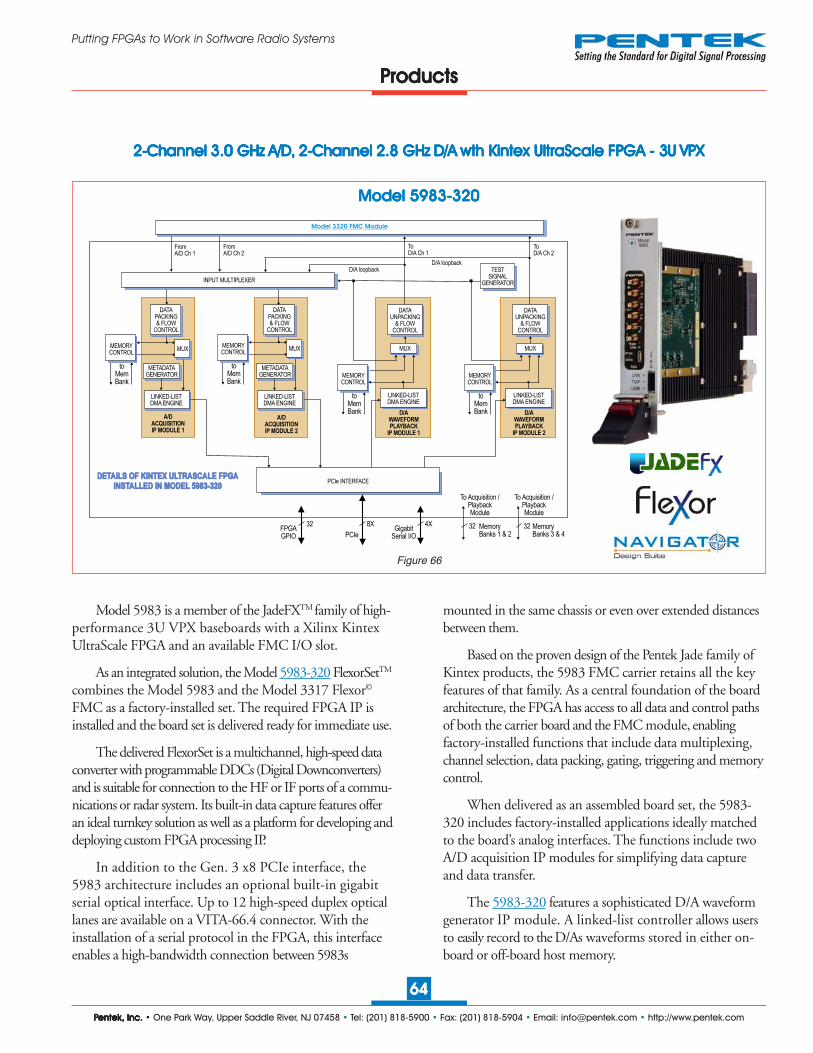
PPPPPentek, Inc.entek, Inc.entek, Inc.entek, Inc.entek, Inc. • One Park Way, Upper Saddle River, NJ 07458 • Tel: (201) 818-5900 • Fax: (201) 818-5904 • Email: [email protected] • http://www.pentek.com
6464646464
Putting FPGAs to Work in Software Radio Systems
Figure 66
PPPPProductsroductsroductsroductsroducts
22222-----ChChChChChannelannelannelannelannel 3.0 G3.0 G3.0 G3.0 G3.0 GHz A/D, Hz A/D, Hz A/D, Hz A/D, Hz A/D, 22222-----ChChChChChannelannelannelannelannel 2.8 G2.8 G2.8 G2.8 G2.8 GHz D/A Hz D/A Hz D/A Hz D/A Hz D/A wth Kintex UltraScale FPGA - wth Kintex UltraScale FPGA - wth Kintex UltraScale FPGA - wth Kintex UltraScale FPGA - wth Kintex UltraScale FPGA - 3U VPX3U VPX3U VPX3U VPX3U VPX
Model 5983-320Model 5983-320Model 5983-320Model 5983-320Model 5983-320
Model 5983 is a member of the JadeFXTM family of high-performance 3U VPX baseboards with a Xilinx KintexUltraScale FPGA and an available FMC I/O slot.
As an integrated solution, the Model 5983-320 FlexorSetTM
combines the Model 5983 and the Model 3317 Flexor©
FMC as a factory-installed set. The required FPGA IP isinstalled and the board set is delivered ready for immediate use.
The delivered FlexorSet is a multichannel, high-speed dataconverter with programmable DDCs (Digital Downconverters)and is suitable for connection to the HF or IF ports of a commu-nications or radar system. Its built-in data capture features offeran ideal turnkey solution as well as a platform for developing anddeploying custom FPGA processing IP.
In addition to the Gen. 3 x8 PCIe interface, the5983 architecture includes an optional built-in gigabitserial optical interface. Up to 12 high-speed duplex opticallanes are available on a VITA-66.4 connector. With theinstallation of a serial protocol in the FPGA, this interfaceenables a high-bandwidth connection between 5983s
mounted in the same chassis or even over extended distancesbetween them.
Based on the proven design of the Pentek Jade family ofKintex products, the 5983 FMC carrier retains all the keyfeatures of that family. As a central foundation of the boardarchitecture, the FPGA has access to all data and control pathsof both the carrier board and the FMC module, enablingfactory-installed functions that include data multiplexing,channel selection, data packing, gating, triggering and memorycontrol.
When delivered as an assembled board set, the 5983-320 includes factory-installed applications ideally matchedto the board’s analog interfaces. The functions include twoA/D acquisition IP modules for simplifying data captureand data transfer.
The 5983-320 features a sophisticated D/A waveformgenerator IP module. A linked-list controller allows usersto easily record to the D/As waveforms stored in either on-board or off-board host memory.
PCIe INTERFACE
D/AWAVEFORMPLAYBACK
IP MODULE 2
D/AWAVEFORMPLAYBACK
IP MODULE 1
FromA/D Ch 1
FromA/D Ch 2
ToD/A Ch 2
ToD/A Ch 1
GigabitSerial I/OPCIe
FPGAGPIO
D/A loopbackD/A loopback
DETAILS OF KINTEX ULTRASCALE FPGAINSTALLED IN MODEL 5983-320
DETAILS OF KINTEX ULTRASCALE FPGAINSTALLED IN MODEL 5983-320
A/DACQUISITIONIP MODULE 1
LINKED-LISTDMA ENGINE
METADATAGENERATOR
A/DACQUISITIONIP MODULE 2
LINKED-LISTDMA ENGINE
METADATAGENERATOR
INPUT MULTIPLEXER
DATAUNPACKING
& FLOWCONTROL
DATAUNPACKING
& FLOWCONTROL
TESTSIGNAL
GENERATOR
MUXMUX
LINKED-LISTDMA ENGINE
LINKED-LISTDMA ENGINE
toMemBank
toMemBank
MEMORYCONTROL
MEMORYCONTROL
8X 4X32 MemoryBanks 3 & 4
32MemoryBanks 1 & 2
32
To Acquisition /PlaybackModule
MUX
toMemBank
MEMORYCONTROL
DATAPACKING& FLOW
CONTROL
MUX
toMemBank
MEMORYCONTROL
DATAPACKING& FLOW
CONTROL
To Acquisition /PlaybackModule
Model 3320 FMC Module

PPPPPentek, Inc.entek, Inc.entek, Inc.entek, Inc.entek, Inc. • One Park Way, Upper Saddle River, NJ 07458 • Tel: (201) 818-5900 • Fax: (201) 818-5904 • Email: [email protected] • http://www.pentek.com
6565656565
Putting FPGAs to Work in Software Radio Systems
Figure 67
PPPPProductsroductsroductsroductsroducts
Model 8266 Model 8266 Model 8266 Model 8266 Model 8266
PC Development System for PCIe Cobalt, Onyx, Jade and Flexor BoardsPC Development System for PCIe Cobalt, Onyx, Jade and Flexor BoardsPC Development System for PCIe Cobalt, Onyx, Jade and Flexor BoardsPC Development System for PCIe Cobalt, Onyx, Jade and Flexor BoardsPC Development System for PCIe Cobalt, Onyx, Jade and Flexor Boards
The Model 8266 is a fully-integrated PC develop-ment system for Pentek Cobalt, Onyx, Jade and FlexorPCI Express software radio, data acquisition, and I/Oboards. It was created to save engineers and systemintegrators the time and expense associated with buildingand testing a development system that ensures optimumperformance of Pentek boards.
A fully-integrated system-level solution, the 8266provides the user with a streamlined out-of-the-boxexperience. It comes preconfigured with Pentek hardware,drivers and software examples installed and tested to allowdevelopment engineers to run example applications outof the box.
Pentek ReadyFlow drivers and board supportlibraries are preinstalled and tested with the 8266.ReadyFlow includes example applications with fullsource code, a command line interface for custom
control over hardware, and Pentek’s Signal Analyzer, afull-featured analysis tool that continuously displays livesignals in both time and frequency domains.
Built on a professional 4U rackmount workstation,the 8266 is equipped with the latest Intel processor,DDR3 SDRAM and a high-performance motherboard.These features accelerate application code developmentand provide unhindered access to the high-bandwidthdata available with Cobalt, Onyx, Jade and Flexor analogand digital interfaces. The 8266 can be configuredwith 64-bit Windows or Linux operating systems.
The 8266 uses a 19” 4U rackmount chassis thatis 21” deep. Enhanced forced-air ventilation assuresadequate cooling for Pentek boards. A 1000-W powersupply guarantees more than enough power for addi-tional boards.
Model 8266

PPPPPentek, Inc.entek, Inc.entek, Inc.entek, Inc.entek, Inc. • One Park Way, Upper Saddle River, NJ 07458 • Tel: (201) 818-5900 • Fax: (201) 818-5904 • Email: [email protected] • http://www.pentek.com
6666666666
Putting FPGAs to Work in Software Radio Systems
Figure 68
PPPPProductsroductsroductsroductsroducts
Model 8267 Model 8267 Model 8267 Model 8267 Model 8267
3U OpenVPX Development System for Cobalt, Onyx, Jade and Flexor Boards3U OpenVPX Development System for Cobalt, Onyx, Jade and Flexor Boards3U OpenVPX Development System for Cobalt, Onyx, Jade and Flexor Boards3U OpenVPX Development System for Cobalt, Onyx, Jade and Flexor Boards3U OpenVPX Development System for Cobalt, Onyx, Jade and Flexor Boards
Model 8267
The Model 8267 is a fully-integrated, 3U VPXdevelopment system for Pentek Cobalt, Onyx, Jade andFlexor software radio, data acquisition, and I/O boards.It was created to save engineers and system integratorsthe time and expense associated with building and testing adevelopment system that ensures optimum perfor-mance of Pentek boards.
A fully-integrated system-level solution, the 8267provides the user with a streamlined out-of-the-boxexperience. It comes preconfigured with Pentek hardware,drivers and software examples installed and tested to allowdevelopment engineers to run example applications outof the box.
Pentek ReadyFlow drivers and board support librariesare preinstalled and tested with the 8267. ReadyFlowincludes example applications with full source code, acommand line interface for custom control over
hardware, and Pentek’s Signal Analyzer, a full-featuredanalysis tool that continuously displays live signals inboth time and frequency domains.
Built on a professional 4U rackmount workstation,the 8267 is equipped with the latest Intel i7 processor,DDR3 SDRAM and a high-performance single-boardcomputer. These features accelerate application codedevelopment and provide unhindered access to the high-bandwidth data available with Cobalt, Onyx, Jade andFlexor analog and digital interfaces. The 8267 can beconfigured with 64-bit Windows or Linux operating systems.
The 8267 uses a 19” 4U rackmount chassis that is12” deep. Nine VPX slots provide ample space for anSBC, a switch card and multiple Pentek boards. Enhancedforced-air ventilation assures adequate cooling for allboards and dual 250-W power supplies gurantee morethan adequate power for all installed boards.

PPPPPentek, Inc.entek, Inc.entek, Inc.entek, Inc.entek, Inc. • One Park Way, Upper Saddle River, NJ 07458 • Tel: (201) 818-5900 • Fax: (201) 818-5904 • Email: [email protected] • http://www.pentek.com
6767676767
Putting FPGAs to Work in Software Radio Systems
PPPPProductsroductsroductsroductsroducts
Model 8264 Model 8264 Model 8264 Model 8264 Model 8264
6U OpenVPX Development System for Cobalt, Onyx and Jade Boards6U OpenVPX Development System for Cobalt, Onyx and Jade Boards6U OpenVPX Development System for Cobalt, Onyx and Jade Boards6U OpenVPX Development System for Cobalt, Onyx and Jade Boards6U OpenVPX Development System for Cobalt, Onyx and Jade Boards
Model 8264
with 6U OpenVPX Boards
The Model 8264 is a fully-integrated, 6U VPXdevelopment system for Pentek Cobalt, Onyx and Jadesoftware radio, data acquisition, and I/O boards. It wascreated to save engineers and system integrators the timeand expense associated with building and testing a develop-ment system that ensures optimum performance of Pentekboards.
A fully-integrated system-level solution, the 8264provides the user with a streamlined out-of-the-boxexperience. It comes preconfigured with Pentek hardware,drivers and software examples installed and tested to allowdevelopment engineers to run example applications outof the box.
Pentek ReadyFlow drivers and board supportlibraries are preinstalled and tested with the 8264.ReadyFlow includes example applications with fullsource code, a command line interface for custom
control over hardware, and Pentek’s Signal Analyzer, afull-featured analysis tool that continuously displays livesignals in both time and frequency domains.
Built on a professional 6U rackmount workstation,the 8264 is equipped with the latest Intel i7 processor,DDR3 SDRAM and a high-performance single-boardcomputer. These features accelerate application codedevelopment and provide unhindered access to the high-bandwidth data available with Cobalt, Onyx and Jadeanalog and digital interfaces. The 8264 can be config-ured with 64-bit Windows or Linux operating systems.
The 8264 uses a 19” 6U rackmount chassis that is12” deep. Nine VPX slots provide ample space for anSBC, a switch card and multiple Pentek boards. En-hanced forced-air ventilation assures adequate coolingfor all boards and dual 500-W power supplies guranteemore than adequate power for all installed boards.
Figure 69
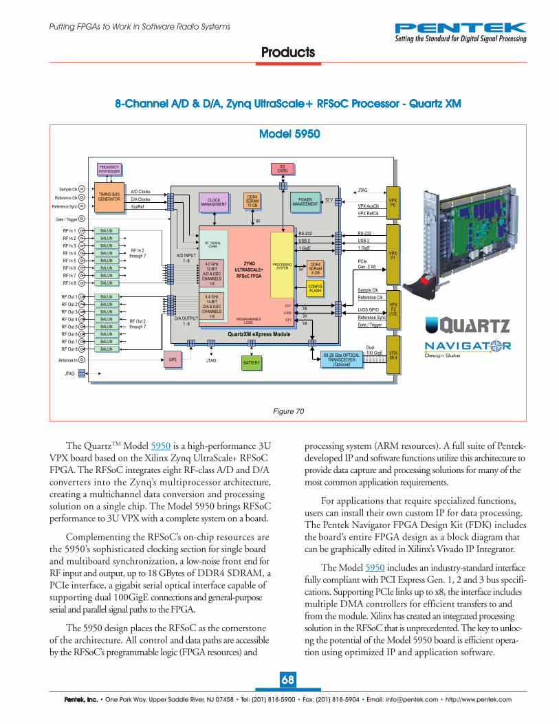
PPPPPentek, Inc.entek, Inc.entek, Inc.entek, Inc.entek, Inc. • One Park Way, Upper Saddle River, NJ 07458 • Tel: (201) 818-5900 • Fax: (201) 818-5904 • Email: [email protected] • http://www.pentek.com
6868686868
Putting FPGAs to Work in Software Radio Systems
Model 5950 Model 5950 Model 5950 Model 5950 Model 5950
Figure 70
8-8-8-8-8-Channel A/D & D/A, Zynq UltraScale+ RFChannel A/D & D/A, Zynq UltraScale+ RFChannel A/D & D/A, Zynq UltraScale+ RFChannel A/D & D/A, Zynq UltraScale+ RFChannel A/D & D/A, Zynq UltraScale+ RFSoC PSoC PSoC PSoC PSoC Processor - Quarrocessor - Quarrocessor - Quarrocessor - Quarrocessor - Quartz XMtz XMtz XMtz XMtz XM
The QuartzTM Model 5950 is a high-performance 3UVPX board based on the Xilinx Zynq UltraScale+ RFSoCFPGA. The RFSoC integrates eight RF-class A/D and D/Aconverters into the Zynq’s multiprocessor architecture,creating a multichannel data conversion and processingsolution on a single chip. The Model 5950 brings RFSoCperformance to 3U VPX with a complete system on a board.
Complementing the RFSoC’s on-chip resources arethe 5950’s sophisticated clocking section for single boardand multiboard synchronization, a low-noise front end forRF input and output, up to 18 GBytes of DDR4 SDRAM, aPCIe interface, a gigabit serial optical interface capable ofsupporting dual 100GigE connections and general-purposeserial and parallel signal paths to the FPGA.
The 5950 design places the RFSoC as the cornerstoneof the architecture. All control and data paths are accessibleby the RFSoC’s programmable logic (FPGA resources) and
processing system (ARM resources). A full suite of Pentek-developed IP and software functions utilize this architecture toprovide data capture and processing solutions for many of themost common application requirements.
For applications that require specialized functions,users can install their own custom IP for data processing.The Pentek Navigator FPGA Design Kit (FDK) includesthe board’s entire FPGA design as a block diagram thatcan be graphically edited in Xilinx’s Vivado IP Integrator.
The Model 5950 includes an industry-standard interfacefully compliant with PCI Express Gen. 1, 2 and 3 bus specifi-cations. Supporting PCIe links up to x8, the interface includesmultiple DMA controllers for efficient transfers to andfrom the module. Xilinx has created an integrated processingsolution in the RFSoC that is unprecedented. The key to unloc-ng the potential of the Model 5950 board is efficient opera-tion using optimized IP and application software.
PPPPProductsroductsroductsroductsroducts

PPPPPentek, Inc.entek, Inc.entek, Inc.entek, Inc.entek, Inc. • One Park Way, Upper Saddle River, NJ 07458 • Tel: (201) 818-5900 • Fax: (201) 818-5904 • Email: [email protected] • http://www.pentek.com
6969696969
Putting FPGAs to Work in Software Radio Systems
PPPPProductsroductsroductsroductsroducts
Model 6001 Model 6001 Model 6001 Model 6001 Model 6001
Figure 71
8-8-8-8-8-Channel A/D & D/A, Zynq UltraScale+ RFChannel A/D & D/A, Zynq UltraScale+ RFChannel A/D & D/A, Zynq UltraScale+ RFChannel A/D & D/A, Zynq UltraScale+ RFChannel A/D & D/A, Zynq UltraScale+ RFSoC PSoC PSoC PSoC PSoC Processor - Quarrocessor - Quarrocessor - Quarrocessor - Quarrocessor - Quartz XMtz XMtz XMtz XMtz XM
The Quartz Model 6001 is a high-performanceQuartz eXpress Module (QuartzXM) based on the XilinxZynq UltraScale+ RFSoC FPGA. The RFSoC FPGAintegrates eight RF-class A/D and D/A converters into theZynq’s multiprocessor architecture, creating a multichanneldata conversion and processing solution on a single chip.
The Model 6001 has ben designed to bring RFSoCperformance to a wide range of different applications byoffering the FPGA in a small system on module solutionmeasuring only 2.5 by 4.0 inches. In addition to the RFSoCFPGA, the 6001 includes all of the support circuitry neededto maximize the performance of the RFSoC.
The 6001 is available on standard form factor carriers.The Pentek Model 5950 delivers the 6001 as a 3U Open-VPX Commercial Off -The-Shelf (COTS) board availablein air cooled and full rugged and conduction cooledversions. In many applications, the 3U VPX standard form
factor carrier can provide a final, deployable turnkeysolution.
In situations where only a custom form factor willsatisfy the application requirements, Pentek supports the6001 with a design kit for users to engineer and build theirown custom carrier. As a complete and tested module, theQuartzXM encapsulates best in class electrical and mechani-cal design, eliminating some of the most challenging aspectsof embedded circuit design and allowing the user to focuson the application specific carrier design.
The 6001 board design positions the RFSoC as thecornerstone of the architecture. All control and data pathsare accessible by the RFSoC’s programmable logic and proces-sing system. A full suite of Pentek-developed IP and softwarefunctions utilize this architecture to provide data capture,generation and processing solutions for many of themost common application requirements.

PPPPPentek, Inc.entek, Inc.entek, Inc.entek, Inc.entek, Inc. • One Park Way, Upper Saddle River, NJ 07458 • Tel: (201) 818-5900 • Fax: (201) 818-5904 • Email: [email protected] • http://www.pentek.com
7070707070
Putting FPGAs to Work in Software Radio Systems
Figure 72
ComplementarComplementarComplementarComplementarComplementary Py Py Py Py Productsroductsroductsroductsroducts
RF In
USB
I/QDOWNCONVERTER
SYNTHESIZER
Ref In
RF InI/Q
DOWNCONVERTER
SYNTHESIZER
I
Q
I
Q
Gain 1 Control
Gain 2 Control
Tuning Control
USBINTERFACE
Gain 1 Control
Gain 1 Control
Tuning Control
Tuning Control
IF I Out
IF Q Out
IF I Out
IF Q Out
(option 015)
Ref Out
OVENCONTROLLEDREFERENCEOSCILLATOR
(optional)
LOWPASSOR
BANDPASSFILTER
Gain 2 Control
(optional)
LOWPASSOR
BANDPASSFILTER
Gain 2 Control
LOWNOISEAMP
LOWNOISEAMP
LOWNOISEAMP
LOWNOISEAMP
LOWNOISEAMP
LOWNOISEAMP
Model 7820 PCIe
The Bandit® Model 7820 is a two-channel, high-performance, stand-alone analog RF wideband down-converter. Packaged in a small, shielded PCIe boardwith front-panel connectors for easy integration into RFsystems, the board offers programmable gain, highdynamic range and a low noise figure.
With an input frequency range from 400 to 4000MHz and a wide IF bandwidth of up to 390 MHz, the7820 is an ideal solution for amplifying and downconvertingantenna signals for communications, radar and SIGINT.
The 7820 accepts RF signals on two front-panelSSMC connectors. LNAs (Low Noise Amplifiers) areprovided, along with two programmable attenuatorsallowing downconversion of input signals ranging from–60 dBm to –20 dBm in steps of 0.5 dB. Higher levelsignals can be attenuated prior to input. An optionalfive-stage lowpass or bandpass input filter can beincluded with several available frequency and attenuationcharacteristics for RF image rejection and harmonic
suppression. The 7820 features a pair of AnalogDevices ADL5380 quadrature mixers. The ADL5380’sare capable of excellent accuracy with amplitude and phasebalances of ~0.07 dB and ~0.2°, respectively.
The 7820 uses an Analog Devices ADF4351 low-noise, on-board frequency synthesizer as the LO (LocalOscillator). Locked to an external input reference foraccuracy with a fractional-N phase-locked loop, itsfrequency is programmable across the 400 to the 4000 MHzband with a tuning resolution of better than 100 kHz.
Output is provided as baseband I and Q signals atbandwidths up to 390 MHz. User-provided in-line outputIF filters allow customizing the output bandwidth andoffset frequency to the specific application requirements.
Versions of the 7820 are also available as an XMCmodule (Model 7120), 3U VPX (Models 5220 and 5320),6U VPX (Models 5720 and 5820 with dual density),AMC (Model 5620), 6U cPCI (Models 7220 and 7420with dual density), and 3U cPCI (Model 7320).
Bandit TBandit TBandit TBandit TBandit Twowowowowo-----Channel Analog RF WChannel Analog RF WChannel Analog RF WChannel Analog RF WChannel Analog RF Wideband Downconverideband Downconverideband Downconverideband Downconverideband Downconverterterterterter
Model 7820 - PCIeModel 7820 - PCIeModel 7820 - PCIeModel 7820 - PCIeModel 7820 - PCIe

PPPPPentek, Inc.entek, Inc.entek, Inc.entek, Inc.entek, Inc. • One Park Way, Upper Saddle River, NJ 07458 • Tel: (201) 818-5900 • Fax: (201) 818-5904 • Email: [email protected] • http://www.pentek.com
7171717171
Putting FPGAs to Work in Software Radio Systems
RF SWITCH
RF In IF Out
RefIn
ExtLOIn
BANDPASSFILTER
STEPATTENUATOR
STEPATTENUATOR
MIXER IF FILTER
RF Attenuation
IF Attenuation
LO Select
LO Synthesizer Tuning Frequency
USBINTERFACE
LOWNOISEAMP
GAINBLOCK
GAINBLOCK
GAINBLOCK
GAINBLOCK
ControlIn
OVENCONTROLLED
CRYSTALOSCILLATOR
RefOut
LO
Model 8111 Model 8111 Model 8111 Model 8111 Model 8111
Figure 73
Bandit Modular Analog RF DownconverBandit Modular Analog RF DownconverBandit Modular Analog RF DownconverBandit Modular Analog RF DownconverBandit Modular Analog RF Downconverter Seriester Seriester Seriester Seriester Series
The Bandit Model 8111 provides a series of high-perfor-mance, stand-alone RF slot receiver modules. Packaged ina small, shielded enclosure with connectors for easyintegration into RF systems, the modules offer programmablegain, high dynamic range and a low noise figure. Withinput options to cover specific frequency bands of the RFspectrum, and an IF output optimized for A/D converters,the 8111 is an ideal solution for amplifying and down-converting antenna signals for communications, radar andsignal intelligence systems.
The 8111 accepts RF signals on a front panel SMAconnector. An LNA (Low Noise-figure Amplifier) isprovided along with two programmable attenuatorsallowing downconversion of input signals ranging from–60 dBm to –20 dBm in steps of 0.5 dB. Higher levelsignals can be attenuated prior to input.
Seven different input-frequency band options areoffered, each tunable across a 400 MHz band, with anoverlap of 100 MHz between adjacent bands. As agroup, these seven options accommodate RF inputsignals from 800 MHz to 3.000 GHz as follows:
Option Frequency Band001 800-1200 MHz002 1100-1500 MHz003 1400-1800 MHz004 1700-2100 MHz005 2000-2400 MHz006 2300-2700 MHz007 2600-3000 MHz
An 80 MHz wide IF output is provided at a 225 MHzcenter frequency . This output is suitable for A/D conver-sion using Pentek high-performance signal acquisitionproducts, such as those in the Cobalt and Onyx families.
Model 8111
ComplementarComplementarComplementarComplementarComplementary Py Py Py Py Productsroductsroductsroductsroducts

PPPPPentek, Inc.entek, Inc.entek, Inc.entek, Inc.entek, Inc. • One Park Way, Upper Saddle River, NJ 07458 • Tel: (201) 818-5900 • Fax: (201) 818-5904 • Email: [email protected] • http://www.pentek.com
7272727272
Putting FPGAs to Work in Software Radio Systems
Figure 74
Model 7192PMC/XMC
PLL&
DIVIDER
Gate / Trigger Out
Sample Clk /Reference
Clk InMUX
ClkIn
RefIn
:N
PROGRAMMABLEVCXO
Clock /Calibration Out
:N
BUFFER&
PROGRAMDELAYS
Clk/RefIn
Sync OutReference Clk Out
TWSI Control InReference Clk In *
Gate / Trigger OutSync OutReference Clk Out
MUX
Trig/GateIn
SyncIn
TWSICONTROL
Gate / Trigger OutSync OutReference Clk Out
Gate / Trigger OutSync OutReference Clk Out
Gate / Trigger In
Sync In
�Sync 3
�Sync 2
�Sync 1
�Sync 4
* For 71640 A/D calibration
The Model 7192 High-Speed Synchronizer andDistribution Board synchronizes multiple Pentek Cobaltor Onyx modules within a system. It enables synchronoussampling and timing for a wide range of multichannelhigh-speed data acquisition, DSP, and software radioapplications. Up to four modules can be synchronizedusing the 7192, with each receiving a common clockalong with timing signals that can be used for synchro-nizing, triggering and gating functions.
Model 7192 provides three front panel MMCXconnectors to accept input signals from external sources:one for clock, one for gate or trigger and one for a synchro-nization signal. Clock signals can be applied from anexternal source such as a high performance sine-wavegenerator. Gate/trigger and sync signals can come froman external system source. In addition to the MMCXconnector, a reference clock can be accepted through thefirst front panel µSync output connector, allowing asingle Cobalt or Onyx board to generate the clock forall subsequent boards in the system.
The 7192 provides four front panel µSync outputconnectors, compatible with a range of high-speedPentek Cobalt and Onyx modules. The µSync signalsinclude a reference clock, gate/trigger and sync signals and aredistributed through matched cables, simplifying systemdesign. The 7192 features a calibration output specifi-cally designed to work with the 71640 or 717403.6 GHz A/D module and provide a signal reference forphase adjustment across multiple D/As.
The 7192 supports all high-speed models in the Cobaltand Onyx families including the 71630/71730 1 GHz A/Dand D/A XMC, the 71640/71741 3.6 GHz A/D XMCand the 71670/71771 Four-channel 1.25 GHz, 16-bitD/A XMC.
Versions of the 7192 are also available as a PCIe half-length board (Model 7892), 3U VPX (Model 5292), 6UVPX (Models 5792 and 5892 with dual density),AMC (Model 5692), 6U cPCI (Models 7292 and 7492dual density), and 3U cPCI (Model 7392).
ComplementarComplementarComplementarComplementarComplementary Py Py Py Py Productsroductsroductsroductsroducts
Model 7192 - PMC/XMCModel 7192 - PMC/XMCModel 7192 - PMC/XMCModel 7192 - PMC/XMCModel 7192 - PMC/XMC
High-Speed Synchronizer and Distribution BoardHigh-Speed Synchronizer and Distribution BoardHigh-Speed Synchronizer and Distribution BoardHigh-Speed Synchronizer and Distribution BoardHigh-Speed Synchronizer and Distribution Board

PPPPPentek, Inc.entek, Inc.entek, Inc.entek, Inc.entek, Inc. • One Park Way, Upper Saddle River, NJ 07458 • Tel: (201) 818-5900 • Fax: (201) 818-5904 • Email: [email protected] • http://www.pentek.com
7373737373
Putting FPGAs to Work in Software Radio Systems
Figure 75
Model 7893 - Half-length PCIeModel 7893 - Half-length PCIeModel 7893 - Half-length PCIeModel 7893 - Half-length PCIeModel 7893 - Half-length PCIe
System Synchronizer and Distribution BoardSystem Synchronizer and Distribution BoardSystem Synchronizer and Distribution BoardSystem Synchronizer and Distribution BoardSystem Synchronizer and Distribution Board
PLL&
DIVIDER
CLKIN
PROGRAMVCXO
Clock Out 1: N
BUFFER&
PROGRAMDELAYS
TTLSync / PPS B In
Timing Bus Out 2through
Timing Bus Out 7
USBINTERFACE
USB
Sample Clk A
Sample Clk BGate / Trig AGate / Trig B
Sync / PPS ASync / PPS B
Timing Bus In
Sample Clk ASample Clk BGate / Trig AGate / Trig BSync / PPS A
Sync / PPS B
Timing Bus Out 1
Sample Clk ASample Clk BGate / Trig AGate / Trig BSync / PPS A
Sync / PPS B
Timing Bus Out 8
MUX
TTLSync / PPS A In
MUX
MUX
MUX
TTLGate / Trig In
MUX
Sample Clk /Reference Clk In
Clock Out 2
Clock Out 3
Clock Out 4
: N
: N
: N
: N
Gate / Trig A
Gate / Trig B
Sync / PPS A
Sync / PPS B
MUX
USB Sync / PPS
USB Gate / Trig
REFCLKIN
CONTROLVOLTAGE
Sample Clk A
Sample Clk B
Sample Clk A
Sample Clk B
Control
USB Gate / Trig
USB Sync / PPS
Model 7893 System Synchronizer and DistributionBoard synchronizes multiple Pentek Cobalt and Onyxboards within a system. It enables synchronous sampling,playback and timing for a wide range of multichannelhigh-speed data acquisition, DSP and software radioapplications.
Up to eight boards can be synchronized using the7893, each receiving a common clock up to 800 MHzalong with timing signals that can be used for synchroniz-ing, triggering and gating functions. For larger systems,up to eight 7893s can be linked together to provide synchro-nization for up to 64 Cobalt or Onyx boards.
The Model 7893 provides four front panel SMAconnectors to accept LVTTL input signals fromexternal sources: two for Sync/PPS and one for Gate/Trigger. In addition to the synchronization signals, a frontpanel SMA connector accepts sample clocks up to 800 MHzor, in an alternate mode, accepts a 10 MHz referenceclock to lock an on-board VCXO sample clock source.
The 7893 provides eight timing bus output connec-tors for distributing all needed timing and clock signalsto the front panels of Cobalt and Onyx boards via ribboncables. The 7893 locks the Gate/Trigger and Sync/PPSsignals to the system’s sample clock. The 7893 alsoprovides four front panel SMA connectors for distrib-uting sample clocks to other boards in the system.
The 7893 can accept a clock from either the front panelSMA connector or from the timing bus input connector. Aprogrammable on-board VCXO clock generator can belocked to a user-supplied, 10 MHz reference.
The 7893 supports a wide range of products in theCobalt family including the 78620 and 78621 three-channelA/D 200 MHz transceivers, the 78650 and 78651 two-channelA/D 500 MHz transceivers, the 78660, 78661 and 78662four-channel 200 MHz A/Ds, and the 78690 L-Band RFTuner. The 7893 also supports the Onyx 78760 four-channel 200 MHz A/D and all complementary modelsin the Onyx family.
Model 7893PCIe
ComplementarComplementarComplementarComplementarComplementary Py Py Py Py Productsroductsroductsroductsroducts

PPPPPentek, Inc.entek, Inc.entek, Inc.entek, Inc.entek, Inc. • One Park Way, Upper Saddle River, NJ 07458 • Tel: (201) 818-5900 • Fax: (201) 818-5904 • Email: [email protected] • http://www.pentek.com
7474747474
Putting FPGAs to Work in Software Radio Systems
Figure 76
FREQUENCYSYNTHESIZER
OVENSTABlLIZED
OSCILLATOR
Clock Out 1
ReferenceClock In
Clock Out 2
frequency setby board option
Clock Out 4
REFERENCECLOCK
IN
SAMPLECLOCK
OUT
POWERSPLITTER
ReferenceClock Out
Clock Out 3
Model 7194PMC/XMC
Model 7194 High-Speed Clock Generator providesfixed-frequency sample clocks to Cobalt and Onyxmodules in multiboard systems. It enables synchronoussampling, playback and timing for a wide range ofmultichannel high-speed data acquisition and softwareradio applications.
The Model 7194 uses a high-precision, fixed-frequency, PLO (Phase-Locked Oscillator) to generatean output sample clock. The PLO accepts a 10 MHzreference clock through a front panel SMA connector.The PLO locks the output sample clock to the incomingreference. A power splitter then receives the sample clockand distributes it to four front panel SMA connectors.
The 7194 is available with sample clock frequenciesfrom 1.4 to 2.0 GHz.
In addition to accepting a reference clock on the frontpanel, the 7194 includes an on-board 10 MHzreference clock. The reference is an OCXO (Oven-Controlled Crystal Oscillator), which provides anexceptionally precise frequency standard with excellentphase noise characteristics.
The 7194 is a standard PMC/XMC module. Themodule does not require programming and the PMCP14 or XMC P15 connector is used solely for power.The module can be optionally configured with a PCIe-style 6-pin power connector allowing it to be used invirtually any chassis or enclosure.
Versions of the 7194 are also available as a PCIe half-length board (Model 7894), 3U VPX (Model 5294),6U VPX (Models 5794 and 5894 with dual density),AMC (Model 5694), 6U cPCI (Models 7294 and 7494dual density), and 3U cPCI (Model 7394).
ComplementarComplementarComplementarComplementarComplementary Py Py Py Py Productsroductsroductsroductsroducts
Model 7194 - PMC/XMCModel 7194 - PMC/XMCModel 7194 - PMC/XMCModel 7194 - PMC/XMCModel 7194 - PMC/XMC
High-Speed Clock GeneratorHigh-Speed Clock GeneratorHigh-Speed Clock GeneratorHigh-Speed Clock GeneratorHigh-Speed Clock Generator

PPPPPentek, Inc.entek, Inc.entek, Inc.entek, Inc.entek, Inc. • One Park Way, Upper Saddle River, NJ 07458 • Tel: (201) 818-5900 • Fax: (201) 818-5904 • Email: [email protected] • http://www.pentek.com
7575757575
Putting FPGAs to Work in Software Radio Systems
High-Speed System Synchronizer UnitHigh-Speed System Synchronizer UnitHigh-Speed System Synchronizer UnitHigh-Speed System Synchronizer UnitHigh-Speed System Synchronizer Unit
Model 9192 - RModel 9192 - RModel 9192 - RModel 9192 - RModel 9192 - Rackmountackmountackmountackmountackmount
PLL&
DIVIDER
Gate / Trigger Out
Sample Clk /Reference
Clk InMUX
ClkIn
RefIn
:N
PROGRAMMABLEVCXO
Clock Out 1
:N
BUFFER&
PROGRAMDELAYS
ClkRefIn
Sync OutReference Clk Out
TWSI Control InReference Clk In *
Gate / Trigger OutSync OutReference Clk Out
MUX
Trig/GateIn
SyncIn
TWSICONTROL
Gate / Trigger OutSync OutReference Clk Out
Gate / Trigger In
Sync In
�Sync 2
�Sync 1
�Sync 12
* For 71640 A/D calibration
�Sync 3through
�Sync 11
Clock Out 2
Clock Out 12
CLOCKSPLITTER
Clock Out 3throughClock Out 11
External Clk In
MUX
USB-TO-TWSIINTERFACE
USB
Model 9192
Model 9192 Rack-mount High-Speed SystemSynchronizer Unit synchronizes multiple Pentek Cobalt orOnyx modules within a system. It enables synchronoussampling and timing for a wide range of multichannelhigh-speed data acquisition, DSP, and software radioapplications. Up to twelve boards can be synchronizedusing the 9192, each receiving a common clock alongwith timing signals that can be used for synchronizing,triggering and gating functions.
Model 9192 provides four rear panel SMA connec-tors to accept input signals from external sources: twofor clock, one for gate or trigger and one for a synchro-nization signal. Clock signals can be applied from anexternal source such as a high performance sine-wavegenerator. Gate/trigger and sync signals can come from anexternal system source. In addition to the SMA connector,a reference clock can be accepted through the first rearpanel µSync output connector, allowing a single Cobaltor Onyx board to generate the clock for all subsequentboards in the system.
The 9192 provides four rear panel µSync outputconnectors, compatible with a range of high-speed PentekCobalt and Onyx boards. The µSync signals include areference clock, gate/trigger and sync signals and are distrib-uted through matched cables, simplifying system design.
The 9192 features twelve calibration outputsspecifically designed to work with the 71640 or 717413.6 GHz A/D modules and provides a signal referencefor phase adjustment across multiple D/As.
The 9192 allows programming of operation parametersincluding: VCXO frequency, clock dividers, and delays thatallow the user to make timing adjustments on the gate andsync signals. These adjustments are made before they are sentto buffers for output through the µSync connectors.
The 9192 supports all high-speed models in the Cobaltfamily including the 71630 1 GHz A/D and D/A XMC, the71640 3.6 GHz A/D XMC and the 71670 Four-channel1.25 GHz, 16-bit D/A XMC. The 9192 also supports high-speed models in the Onyx family.
Figure 77
ComplementarComplementarComplementarComplementarComplementary Py Py Py Py Productsroductsroductsroductsroducts

PPPPPentek, Inc.entek, Inc.entek, Inc.entek, Inc.entek, Inc. • One Park Way, Upper Saddle River, NJ 07458 • Tel: (201) 818-5900 • Fax: (201) 818-5904 • Email: [email protected] • http://www.pentek.com
7676767676
Putting FPGAs to Work in Software Radio Systems
RTX Rackmountsystem
High-Speed Recording Systems
Talon® High-Speed Recording Systems eliminate thetime and risk associated with new technology systemdevelopment. With increasing pressure in both the defenseand commercial arenas to get to the market first, today’ssystem engineers are looking for more complete off-the-shelfsystem offerings.
Out of the box, these systems arrive complete witha full-featured virtual operator control panel ready forimmediate data recording and/or playback operation.
Because they consist of modular COTS board-levelproducts and the flexible Pentek SystemFlow® software, theyare easily scalable to larger multichannel data acquisitionand recording applications requiring aggregate recordingrates of up to 5.0 GB/sec.
Ready-to-Run Recording Systems
Depending on model, the Pentek offerings are fullyintegrated systems featuring a range of A/D and D/Aresources or digital I/O with high-speed disk arrays.
These systems are built on a Windows workstationand they are presented in this section because they caneasily satisfy a broad spectrum of recording needs.Furthermore, users can easily install postprocessing andanalysis tools to operate on the recorded data which isstored in the familiar NTFS format.
Recording Systems Form Factors
Pentek’s High-Speed Recording Systems are available asRTV and RTS Lab Systems and are housed in a 19-in.rack-mountable chassis in a PC server configuration. They aredesigned for commercial applications in a lab or office environment.
RTR Portable Systems are available in a small briefcase-sized enclosures with integral LCD display and keyboard.They, too, provide a PC server configuration and are designedfor harsh environment field applications where size and weight isof paramount importance.
RTR Rugged Rackmount Systems are housed in a 19-in.rugged rack-mountable chassis. They are built to survive shockand vibration and they target operation in harsh environmentsand remote locations that may be unsuitable for humans.
RTX Extreme Systems are available in a rackmountor portable chassis designed to military specs. They aredesigned to operate under extreme environmentalconditions using forced-air or conduction-cooling to drawheat from system components.
TTTTTalonalonalonalonalon High-Speed RHigh-Speed RHigh-Speed RHigh-Speed RHigh-Speed Recording Systems: Flexible and Deployable Solutionsecording Systems: Flexible and Deployable Solutionsecording Systems: Flexible and Deployable Solutionsecording Systems: Flexible and Deployable Solutionsecording Systems: Flexible and Deployable Solutions
RTS Lab system
RTR Rackmountsystem
RTR Portable System
ComplementarComplementarComplementarComplementarComplementary Py Py Py Py Productsroductsroductsroductsroducts
RTV Recording Systems areexcellent value for under
$20,000 US
RTS Recording Systems aredesigned for commercial
applications
RTR Recording Systems aredesigned for harsh
environments
RTX Recording Systems aredesigned for extreme
environments
ANALOG RECORDERS
DIGITAL RECORDERSRTX Portable
system

PPPPPentek, Inc.entek, Inc.entek, Inc.entek, Inc.entek, Inc. • One Park Way, Upper Saddle River, NJ 07458 • Tel: (201) 818-5900 • Fax: (201) 818-5904 • Email: [email protected] • http://www.pentek.com
7777777777
Putting FPGAs to Work in Software Radio Systems
Figure 79
PPPPPentek SystemFlow Rentek SystemFlow Rentek SystemFlow Rentek SystemFlow Rentek SystemFlow Recording Sofecording Sofecording Sofecording Sofecording Software for Analog Rtware for Analog Rtware for Analog Rtware for Analog Rtware for Analog Recordersecordersecordersecordersecorders
Signal Viewer
Recorder Interface
Hardware Configuration
The Pentek SystemFlow Recording Software for AnalogRecorders provides a rich set of function libraries and toolsfor controlling all Pentek analog high-speed real-timerecording systems. SystemFlow software allows developersto configure and customize system interfaces and behavior.
The Recorder Interface shows a system block diagramand includes configuration, record, playback and statusscreens, each with intuitive controls and indicators. Theuser can easily move between screens to set configurationparameters, control and monitor a recording, play backa recorded signal and monitor board temperatures andvoltage levels.
The Hardware Configuration screen provides asimple and intuitive means for setting up the systemparameters. The configuration screen shown here, allowsuser entries for input source, center frequency, decima-tion, as well as gate and trigger information. All
parameters contain limit-checking and integrated helpto provide an easier-to-use out-of-the-box experience.
The SystemFlow Signal Viewer includes a virtualoscilloscope and spectrum analyzer for signal monitoringin both the time and frequency domains. It is extremelyuseful for previewing live inputs prior to recording, andfor monitoring signals as they are being recorded to helpensure successful recording sessions. The viewer can alsobe used to inspect and analyze the recorded files after therecording is complete.
Advanced signal analysis capabilities include automaticcalculators for signal amplitude and frequency, secondand third harmonic components, THD (total harmonicdistortion) and SINAD (signal to noise and distortion).With time and frequency zoom, panning modes and dualannotated cursors to mark and measure points of interest,the Signal Viewer can often eliminate the need for a separateoscilloscope or spectrum analyzer in the field.
ComplementarComplementarComplementarComplementarComplementary Py Py Py Py Productsroductsroductsroductsroducts
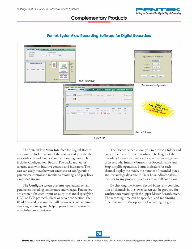
PPPPPentek, Inc.entek, Inc.entek, Inc.entek, Inc.entek, Inc. • One Park Way, Upper Saddle River, NJ 07458 • Tel: (201) 818-5900 • Fax: (201) 818-5904 • Email: [email protected] • http://www.pentek.com
7878787878
Putting FPGAs to Work in Software Radio Systems
Figure 80
PPPPPentek SystemFlow Rentek SystemFlow Rentek SystemFlow Rentek SystemFlow Rentek SystemFlow Recording Sofecording Sofecording Sofecording Sofecording Software for Digital Rtware for Digital Rtware for Digital Rtware for Digital Rtware for Digital Recordersecordersecordersecordersecorders
The SystemFlow Main Interface for Digital Record-ers shows a block diagram of the system and provides theuser with a control interface for the recording system. Itincludes Configuration, Record, Playback, and Statusscreens, each with intuitive controls and indicators. Theuser can easily move between screens to set configurationparameters, control and monitor a recording, and play backa recorded stream.
The Configure screen presents operational systemparameters including temperature and voltages. Parametersare entered for each input or output channel specifyingUDP or TCP protocol, client or server connection, theIP address and port number. All parameters contain limit-checking and integrated help to provide an easier-to-useout-of-the-box experience.
The Record screen allows you to browse a folder andenter a file name for the recording. The length of therecording for each channel can be specified in megabytesor in seconds. Intuitive buttons for Record, Pause andStop simplify operation. Status indicators for eachchannel display the mode, the number of recorded bytes,and the average data rate. A Data Loss indicator alertsthe user to any problem, such as a disk- full condition.
By checking the Master Record boxes, any combina-tion of channels in the lower screen can be grouped forsynchronous recording via the upper Master Record screen.The recording time can be specified, and monitoringfunctions inform the operator of recording progress.
Record Screen
Main Interface
Hardware Configuration
ComplementarComplementarComplementarComplementarComplementary Py Py Py Py Productsroductsroductsroductsroducts

PPPPPentek, Inc.entek, Inc.entek, Inc.entek, Inc.entek, Inc. • One Park Way, Upper Saddle River, NJ 07458 • Tel: (201) 818-5900 • Fax: (201) 818-5904 • Email: [email protected] • http://www.pentek.com
7979797979
Putting FPGAs to Work in Software Radio Systems
Figure 81
AnalogInput
AnalogOutput
200 MHz16-bit A/D
DIGITALDOWN-
CONVERTERDecimation:2 to 65,536
INTELPROCESSOR
SYSTEM DRIVEDDR
SDRAM
HOST PROCESSORRUNNING SYSTEMFLOW
4 TB DATA STORAGE
DATA DRIVES DATA DRIVES
DATA DRIVES DATA DRIVES
MODEL RTV 2601
USB
GigabitEthernet
PS/2Keyboard
PS/2Mouse
VideoOutput
GPSAntenna(Optional)
800 MHz16-bit D/A
DIGITALUP-
CONVERTERDecimation:2 to 65,536
Model RTV 2601 Model RTV 2601 Model RTV 2601 Model RTV 2601 Model RTV 2601
200 MS/sec RF/IF R200 MS/sec RF/IF R200 MS/sec RF/IF R200 MS/sec RF/IF R200 MS/sec RF/IF Rackmount Rackmount Rackmount Rackmount Rackmount Recorderecorderecorderecorderecorder
The Talon RTV 2601 is a turnkey multibandrecording and playback system used for recording andreproducing signals with bandwidths up to 80 MHz.The RTV 2601 uses a 16-bit, 200 MHz A/D converterto provide real-time sustained recording rates to disk ofup to 400 MB/sec. The A/D is complemented with a16-bit 800 MHz D/A that provides the ability to reproducesignals captured in the field.
The RTV 2601 comes in a 4U 19 in. rackmountpackage that is 22.75 in. deep. Signal I/O is provided inthe rear of the unit, while the hot-swappable data drivesare available at the front. Air is pulled through the systemfrom front to back allowing it to operate at ambienttemperatures from 5 to 35 deg C.
The RTV 2601 includes a programmable digitaldownconverter so users can configure the system to capturesignals with frequencies as low as 300 kHz and as high as700 MHz. Corresponding signal bandwidths range from
a few kilohertz to 80 MHz. A digital upconverter andD/A produce an analog output matching the recordedIF signal frequency.
The system includes a built-in sample clocksynthesizer programmable to any desired frequencyfrom 10 MHz to 200 MHz. This clock synthesizer can belocked to an external 10 MHz reference clock and hasexcellent phase noise characteristics. Alternately, the usercan supply an external sample clock to drive the A/D andD/A converters. The RTV 2601 also supports externaltriggering, allowing users to trigger a recording or playbackon an external signal.
The RTV 2601 includes the Pentek SystemFlow record-ing software. SystemFlow features a Windows-based GUI(Graphical User Interface) that provides a simple means toconfigure and control the recorder. As an option, a GPSor IRIG receiver card can be supplied with the system foraccurate time stamping of recorded data.
Model RTV 2601
ComplementarComplementarComplementarComplementarComplementary Py Py Py Py Productsroductsroductsroductsroducts

PPPPPentek, Inc.entek, Inc.entek, Inc.entek, Inc.entek, Inc. • One Park Way, Upper Saddle River, NJ 07458 • Tel: (201) 818-5900 • Fax: (201) 818-5904 • Email: [email protected] • http://www.pentek.com
8080808080
Putting FPGAs to Work in Software Radio Systems
Figure 82
Model RTV 2602 Model RTV 2602 Model RTV 2602 Model RTV 2602 Model RTV 2602
Serial FPDP RSerial FPDP RSerial FPDP RSerial FPDP RSerial FPDP Rackmount Vackmount Vackmount Vackmount Vackmount Value Ralue Ralue Ralue Ralue Recorderecorderecorderecorderecorder
Model RTV 2602
INTELPROCESSOR
SYSTEM DRIVEDDR
SDRAM
HOST PROCESSORRUNNING SYSTEMFLOW
4 TB DATA STORAGE
DATA DRIVES DATA DRIVES
DATA DRIVES DATA DRIVES
MODEL RTV 2602
USB
GigabitEthernet
Keyboard
Mouse
VideoOutput
GPSAntenna(Optional)
ChannelsIn / Out Serial
FPDP
The Talon RTV 2602 Serial FPDP Value Recorder isdesigned to provide a low-cost solution to users looking tocapture and play back multiple Serial FPDP streams. Itcan record up to four Serial FPDP channels to the built-in 4 TB RAID consisting of cost-effective, enterprise-classHDD storage. It is a complete turnkey recording system,ideal for capturing any type of streaming sources. Theseinclude live transfers from sensors or data from othercomputers and is fully compatible with the VITA 17.1specification.
The RTV 2602 comes in a 4U 19 in. rack-mountpackage that is 22.75 in. deep. Signal I/O is provided inthe rear of the unit, while the hot-swappable data drivesare available in the front. Air is pulled through the systemfrom front to back to allow operation at ambienttemperatures from 5o to 35o C.
The RTV 2606 can be populated with up to four SFPconnectors supporting Serial FPDP over copper, single-
mode, or multi-mode fiber, to accommodate all popularSerial FPDP interfaces. It is capable of both receiving andtransmitting data over these links and supports real-timedata storage to disk.
Programmable modes include flow control in bothreceive and transmit directions, CRC support, and copy/loop modes. The system is capable of handling 1.0625,2.125, 2.5, 3.125 and 4.25 GBaud link rates. Up to fourchannels can be recorded simultaneously with an aggregaterecording rate of up to 400 MB/sec.
As an option, a GPS or IRIG receiver card can besupplied with the system providing accurate time stampingof recorded data. Additionally, the GPS receiver deliversGPS position information that can be recorded along withthe input signals.
The RTV 2602 includes the Pentek SystemFlowrecording software which features a Windows-based GUI.
ComplementarComplementarComplementarComplementarComplementary Py Py Py Py Productsroductsroductsroductsroducts

PPPPPentek, Inc.entek, Inc.entek, Inc.entek, Inc.entek, Inc. • One Park Way, Upper Saddle River, NJ 07458 • Tel: (201) 818-5900 • Fax: (201) 818-5904 • Email: [email protected] • http://www.pentek.com
8181818181
Putting FPGAs to Work in Software Radio Systems
Figure 83
USB
GigabitEthernet
Aux VideoVGA Output
MODEL RTR 2726
ChannelsIn
ChannelsOut
200 MHz16-bit A/D
DIGITAL DOWNCONVERTERDEC: 2 to 64K
800 MHz16-bit D/A
DIGITAL UPCONVERTER
INT: 2 to 512K
INTELPROCESSOR
SYSTEM DRIVEDDR
SDRAM
HOST PROCESSORRUNNING SYSTEMFLOW
HIGH RESOLUTIONVIDEO DISPLAY
RAID DATA STORAGE
DATA DRIVES DATA DRIVES
DATA DRIVES DATA DRIVES
The Talon RTR 2726A is a turnkey, multiband recordingand playback system that allows the user to record andreproduce high-bandwidth signals with lightweight, portableand rugged packages. This model provides aggregaterecording rates of up to 3.2 GB/sec and is ideal for theuser who requires both portability and solid perfor-mance in a compact recording system.
The RTR 2726A is supplied in a small footprint portablepackage measuring only 16.0" W x 6.9" D x 13.0" Hand weighing just less than 30 pounds.
With measurements similar to small briefcases, thisportable workstation includes Intel Core i7 processors,high-resolution 17" LCD monitors, and up to 15.3 TBof SSD storage.
A/D sampling rate, DDC decimation and bandwidth,D/A sampling rate and DUC interpolation are among
the GUI-selectable system parameters, that provide fully-programmable systems capable of recording and reproducinga wide range of signals.
Included with this system is Pentek’s SystemFlowrecording software. Built on a Windows 7 Professionalworkstation with high performance Intel Core i7 processor, thesystem allows the user to install post-processing andanalysis tools to operate on the recorded data. Theyrecord data to the native NTFS file system, providingimmediate access to the data. Custom configurationscan be stored as profiles and later loaded when needed,so users can select preconfigured settings with a single click.
Versions of the RTR 2726A are also available as aRackmount Lab unit (Model RTS 2706), Rugged Rackmount(Model RTR 2746), Extreme Rackmount (ModelRTX 2766) and Extreme ½ ATR (Model RTX 2786)
Model RTR 2726A
ComplementarComplementarComplementarComplementarComplementary Py Py Py Py Productsroductsroductsroductsroducts
Model RTR 2726AModel RTR 2726AModel RTR 2726AModel RTR 2726AModel RTR 2726A
200 MS/sec RF/IF R200 MS/sec RF/IF R200 MS/sec RF/IF R200 MS/sec RF/IF R200 MS/sec RF/IF Rugged Pugged Pugged Pugged Pugged Pororororortable Rtable Rtable Rtable Rtable Recorderecorderecorderecorderecorder

PPPPPentek, Inc.entek, Inc.entek, Inc.entek, Inc.entek, Inc. • One Park Way, Upper Saddle River, NJ 07458 • Tel: (201) 818-5900 • Fax: (201) 818-5904 • Email: [email protected] • http://www.pentek.com
8282828282
Putting FPGAs to Work in Software Radio Systems
es
6-
s
-
a-
The Talon RTS 2707 is a turnkey, multiband record-ing and playback system for recording and reproducinghigh-bandwidth signals. The RTS 2707 uses 12-bit,500 MHz A/D converters and provides agregate recordingrates up to 1.6 GB/sec.
The RTS 2707 uses Pentek’s high-powered Virtex-6-based Cobalt modules, that provide flexibility in channelcount, with optional digital downconversion capabilities.Optional 16-bit, 800 MHz D/A converters with digitalupconversion allow real-time reproduction of recordedsignals.
A/D sampling rates, DDC decimations and band-widths, D/A sampling rates and DUC interpolations areamong the GUI-selectable system parameters, providinga fully-programmable system capable of recording andreproducing a wide range of signals. Optional GPS timeand position stamping allows the user to record thiscritical signal information.
The RTS 2707 includes the SystemFlow RecordingSoftware. SystemFlow features a Windows-based GUIthat provides a simple means to configure and control therecorder.
The RTS 2707 is configured in a 4U 19" rack-mountable chassis, with hot-swappable data drives, frontpanel USB ports and I/O connectors on the rear panel.Systems are scalable to accommodate multiple chassis toincrease channel counts and aggregate data rates.
Multiple RAID levels, including 0, 1, 5, 6, 10 and50, provide a choice for the required level of redundancy.The hot-swappable HDDs provide storage capacities ofup to 100 TB in a single 6U chassis.
Versions of the RTS 2707 are available as RuggedPortable (Model RTR 2727), Rugged Rackmount (ModelRTR 2747), and Extreme Rackmount (Model RTX 2767).
Model RTS 2707
INTELPROCESSOR
SYSTEM DRIVEDDR
SDRAM
HOST PROCESSORRUNNING SYSTEMFLOW
RAID DATA STORE
DATA DRIVES DATA DRIVES
DATA DRIVES DATA DRIVES
MODEL RTS 2707
USB 2.0
GigabitEthernet
PS/2Keyboard
PS/2Mouse
VideoOutput
GPSAntenna(Optional)
ChannelsIn
ChannelsOut
DIGITAL DOWN-CONVERTERDEC: 2 to 64K
800 MHz16-bit D/A
Up to 4Channels
500 MHz12-bit A/D
or400 MHz14-bit A/D
Up to 4Channels
DIGITAL UP-CONVERTERINT: 2 to 64K
Figure 84
ComplementarComplementarComplementarComplementarComplementary Py Py Py Py Productsroductsroductsroductsroducts
Model RTS 2707Model RTS 2707Model RTS 2707Model RTS 2707Model RTS 2707
500 MS/sec RF/IF R500 MS/sec RF/IF R500 MS/sec RF/IF R500 MS/sec RF/IF R500 MS/sec RF/IF Rackmount Lackmount Lackmount Lackmount Lackmount Lab Rab Rab Rab Rab Recorderecorderecorderecorderecorder

PPPPPentek, Inc.entek, Inc.entek, Inc.entek, Inc.entek, Inc. • One Park Way, Upper Saddle River, NJ 07458 • Tel: (201) 818-5900 • Fax: (201) 818-5904 • Email: [email protected] • http://www.pentek.com
8383838383
Putting FPGAs to Work in Software Radio Systems
Figure 85
MODEL RTR 2748
USB
GigabitEthernet
Keyboard
Mouse
VideoOutput
eSATA
GPSAntenna(Optional)
ChannelIn
ChannelOut
1 GHz16-bitD/A
1 GHz12-bitA/D
ChannelIn
ChannelOut
1 GHz16-bitD/A
1 GHz12-bitA/D
(Optional)
INTELPROCESSOR
SYSTEM DRIVEDDR
SDRAM
HOST PROCESSORRUNNING SYSTEMFLOW
RAID DATA STORAGE
DATA DRIVES DATA DRIVES
DATA DRIVES DATA DRIVES
Model RTR 2748
The Talon RTR 2748 is a turnkey recording and playbacksystem that allows users to record and reproduce signalswith bandwidths up to 500 MHz. The RTR 2748 can beconfigured as a one- or two-channel system to providereal-time aggregate recording and playback rates up to4.0 GB/sec to an array of solid-state drives.
The RTR 2748 uses Pentek’s high-powered Virtex-6-based Cobalt boards that provide the data streamingengine for the high-speed A/D converters. A built-insynchronization module is provided to allow for multi-channel phase-coherent operation. GPS time and positionstamping is optionally available.
The RTR 2748 includes the SystemFlow RecordingSoftware. SystemFlow features a Windows-based GUIthat provides a simple means to configure and controlthe system. Custom configurations can be stored as profilesand later loaded when needed, allowing the user to selectpreconfigured settings with a single click.
Built on a Windows 7 Professional workstation,the RTR 2748 allows the user to install post-processingand analysis tools to operate on the recorded data. TheRTR 2748 records data to the native NTFS file systemthat provides immediate access to the recorded data.
Data can be off-loaded via gigabit Ethernet ports, orUSB 2.0 and USB 3.0 ports. Additionally, data can becopied to optical disk, using the 8X double layerDVD±R/RW drive.
Because SSDs operate reliably under conditions of shockand vibration, the RTR 2748 performs well in ground, ship-borne and airborne environments. The drives can be easilyremoved or exchanged during a mission to retrieve the data.
Versions of the RTR 2748 are also available as aRugged Portable (Model RTR 2728), and ExtremeRackmount (Model RTX 2768).
ComplementarComplementarComplementarComplementarComplementary Py Py Py Py Productsroductsroductsroductsroducts
Model RTR 2748 Model RTR 2748 Model RTR 2748 Model RTR 2748 Model RTR 2748
1 GS/sec RF/IF R1 GS/sec RF/IF R1 GS/sec RF/IF R1 GS/sec RF/IF R1 GS/sec RF/IF Rugged Rugged Rugged Rugged Rugged Rackmount Rackmount Rackmount Rackmount Rackmount Recorderecorderecorderecorderecorder

PPPPPentek, Inc.entek, Inc.entek, Inc.entek, Inc.entek, Inc. • One Park Way, Upper Saddle River, NJ 07458 • Tel: (201) 818-5900 • Fax: (201) 818-5904 • Email: [email protected] • http://www.pentek.com
8484848484
Putting FPGAs to Work in Software Radio Systems
Figure 86
Channel 1In 3.6 GHz
(1 Channel)or
1.8 GHz(2 Channel)12-Bit A/D
MODEL RTX 2769
Keyboard
Mouse
VideoOutput
GPSAntenna(Optional)
Channel 2In
USB
GigabitEthernet
INTELPROCESSOR
SYSTEM DRIVEDDR
SDRAM
HOST PROCESSORRUNNING SYSTEMFLOW
RAID DATA STORAGE
DATA DRIVES DATA DRIVES
DATA DRIVES DATA DRIVES
Model RTX 2769
The Talon RTX 2769 is a turnkey system that is built tooperate under harsh conditions. Designed to withstandhigh vibration and operating temperatures, the RTX2769 is intended for military, airborne and UAV applicationsrequiring a rugged system.
Aimed at recording high-bandwidth signals, the RTX 2769uses 12-bit, 3.6 GHz A/D converters. It can be configuredas a one- or two-channel system and can record sampled data,packed as 8-bit- or 16-bit-wide consecutive samples(12-bit digitized samples residing in the 12 MSBs of the16-bit word). A high-speed RAID array provides anaggregate streaming recording rate to disk of 4.8 GB/sec.
The RTX 2769 uses Pentek’s high-powered Virtex-7-based Onyx boards that provide the data streaming enginefor the high-speed A/D converters. Channel and packingmodes as well as gate and trigger settings are among theselectable system parameters, providing completecontrol over this ultra wideband recording system.
Built on a Windows 7 Professional workstation,the RTX 2769 allows the user to install post-processingand analysis tools to operate on the recorded data. TheRTX 2769 records data to the native NTFS file systemthat provides immediate access to the recorded data.
The Talon RTX 2769 uses a shock- and vibration-isolated inner chassis and solid-state drives to assure reliabil-ity under harsh conditions. Developed by Pentek to enhancethe operation of Extreme recorders, up to four front-panelremovable QuickPacTM drive canisters are provided, eachcontaining up to eight SSDs. Fastened with four thumbscrews,each drive canister can hold up to 7.6 TB of data storageand allows for quick and easy removal of mission-critical datawith a minimum of down time.
Versions of the RTX 2769 are available as a RuggedPortable (Model RTR 2729A), and Rugged Rackmount(Model RTR 2749).
ComplementarComplementarComplementarComplementarComplementary Py Py Py Py Productsroductsroductsroductsroducts
Model RTX 2769 Model RTX 2769 Model RTX 2769 Model RTX 2769 Model RTX 2769
3.6 GS/sec Ultra W3.6 GS/sec Ultra W3.6 GS/sec Ultra W3.6 GS/sec Ultra W3.6 GS/sec Ultra Wideband RF/IF Extreme Rideband RF/IF Extreme Rideband RF/IF Extreme Rideband RF/IF Extreme Rideband RF/IF Extreme Rackmount Rackmount Rackmount Rackmount Rackmount Recorderecorderecorderecorderecorder

PPPPPentek, Inc.entek, Inc.entek, Inc.entek, Inc.entek, Inc. • One Park Way, Upper Saddle River, NJ 07458 • Tel: (201) 818-5900 • Fax: (201) 818-5904 • Email: [email protected] • http://www.pentek.com
8585858585
Putting FPGAs to Work in Software Radio Systems
Figure 87
ComplementarComplementarComplementarComplementarComplementary Py Py Py Py Productsroductsroductsroductsroducts
Model RTS 2620Model RTS 2620Model RTS 2620Model RTS 2620Model RTS 2620
6 GHz RF/IF Sentinel Intelligent Signal Scanning R6 GHz RF/IF Sentinel Intelligent Signal Scanning R6 GHz RF/IF Sentinel Intelligent Signal Scanning R6 GHz RF/IF Sentinel Intelligent Signal Scanning R6 GHz RF/IF Sentinel Intelligent Signal Scanning Rackmount Rackmount Rackmount Rackmount Rackmount Recorderecorderecorderecorderecorder
RF In
RF Out
200 MHz16-bit A/D
DIGITALDOWN-
CONVERTERDecimation:2 to 65,536
INTELPROCESSOR
SYSTEM DRIVEDDR
SDRAM
HOST PROCESSORRUNNING SYSTEMFLOW
RAID DATA STORAGE
DATA DRIVES DATA DRIVES
DATA DRIVES DATA DRIVES
MODEL RTS 2620
USB
GigabitEthernet
Keyboard
Mouse
VideoOutput
GPSAntenna(Optional)
800 MHz16-bit D/A
DIGITALUP-
CONVERTERDecimation:2 to 65,536
6 GHz RFDOWN-
CONVERTER
6 GHz RFUP-
CONVERTER
Model RTS 2620
The Talon RTS 2620 combines the power of a PentekTalon Recording System with those of an RF tuner andRF upconverter hardware plus Pentek’s Sentinel IntelligentSignal Scanner. The RTS 2620 provides SIGINTengineers the ability to scan the 6 GHz spectrum forsignals of interest and monitor or record bandwidths up to40 MHz wide once a signal band of interest is detected.
A spectral scan facility allows the user to sweep thespectrum at 30 GHz/sec, while threshold detection allowsthe system to automatically lock onto and record signalbands. Scan results are displayed in a waterfall plot andcan also be recorded to allow users to look back at someearlier spectral activity.
Once a signal of interest is detected, the real-timerecorder can capture and store hundreds of terabytes ofdata to disk, allowing users to store days worth of data.The optional RF upconverter reproduces signals capturedat RF frequencies up to 6 GHz.
The Pentek Model 78621 Cobalt board transceiverserves as the engine of the RTS 2620 and is coupledwith a 6 GHz tuner to provide excellent dynamic rangeacross the entire spectrum. The 200 MHz 16-bit A/Dboard provides 86 dB of spurious-free dynamic rangeand 74 dB of SNR.
The Virtex-6-based DDC with selectable decimationsof up to 64 k provides exceptional processing gain whileallowing users to zoom into signals of varying bandwidths.All system components are integrated into a rackmountchassis that ranges in size from 3U to 6U depending onstorage requirements. Front panel removable HDDs,configured as a RAID are hot-swappable and configurable.
An optional GPS receiver and built-in PLLs allow alldevices in the RF chain to be locked in phase and correlatedto GPS time. GPS position information can optionallybe recorded, allowing the recorder’s position to be trackedwhile acquiring RF signals. ➤
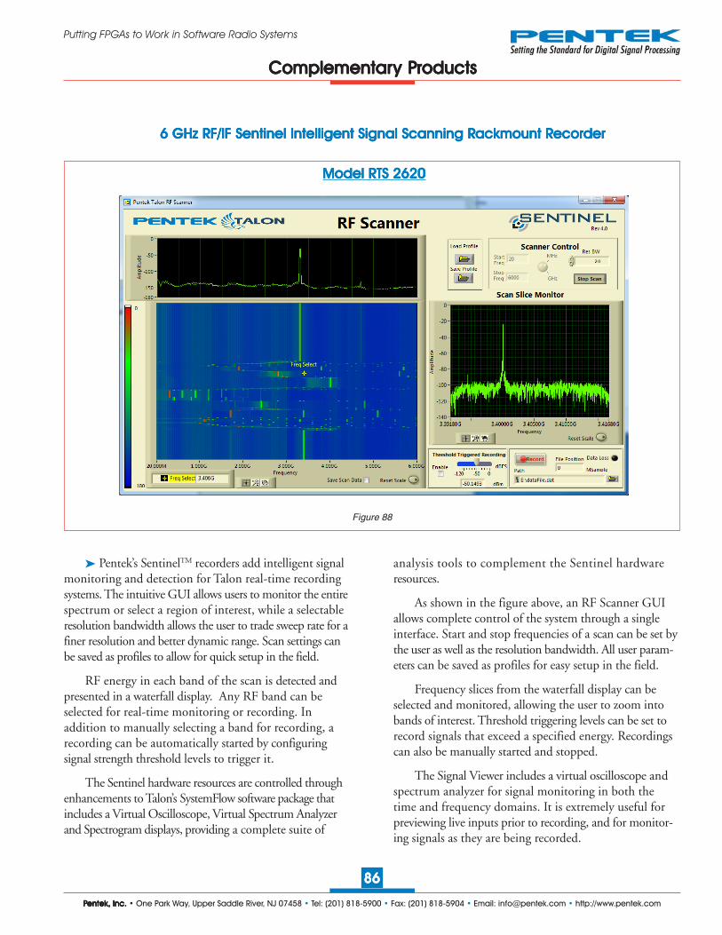
PPPPPentek, Inc.entek, Inc.entek, Inc.entek, Inc.entek, Inc. • One Park Way, Upper Saddle River, NJ 07458 • Tel: (201) 818-5900 • Fax: (201) 818-5904 • Email: [email protected] • http://www.pentek.com
8686868686
Putting FPGAs to Work in Software Radio Systems
Figure 88
ComplementarComplementarComplementarComplementarComplementary Py Py Py Py Productsroductsroductsroductsroducts
Model RTS 2620Model RTS 2620Model RTS 2620Model RTS 2620Model RTS 2620
6 GHz RF/IF Sentinel Intelligent Signal Scanning R6 GHz RF/IF Sentinel Intelligent Signal Scanning R6 GHz RF/IF Sentinel Intelligent Signal Scanning R6 GHz RF/IF Sentinel Intelligent Signal Scanning R6 GHz RF/IF Sentinel Intelligent Signal Scanning Rackmount Rackmount Rackmount Rackmount Rackmount Recorderecorderecorderecorderecorder
➤ Pentek’s SentinelTM recorders add intelligent signalmonitoring and detection for Talon real-time recordingsystems. The intuitive GUI allows users to monitor the entirespectrum or select a region of interest, while a selectableresolution bandwidth allows the user to trade sweep rate for afiner resolution and better dynamic range. Scan settings canbe saved as profiles to allow for quick setup in the field.
RF energy in each band of the scan is detected andpresented in a waterfall display. Any RF band can beselected for real-time monitoring or recording. Inaddition to manually selecting a band for recording, arecording can be automatically started by configuringsignal strength threshold levels to trigger it.
The Sentinel hardware resources are controlled throughenhancements to Talon’s SystemFlow software package thatincludes a Virtual Oscilloscope, Virtual Spectrum Analyzerand Spectrogram displays, providing a complete suite of
analysis tools to complement the Sentinel hardwareresources.
As shown in the figure above, an RF Scanner GUIallows complete control of the system through a singleinterface. Start and stop frequencies of a scan can be set bythe user as well as the resolution bandwidth. All user param-eters can be saved as profiles for easy setup in the field.
Frequency slices from the waterfall display can beselected and monitored, allowing the user to zoom intobands of interest. Threshold triggering levels can be set torecord signals that exceed a specified energy. Recordingscan also be manually started and stopped.
The Signal Viewer includes a virtual oscilloscope andspectrum analyzer for signal monitoring in both thetime and frequency domains. It is extremely useful forpreviewing live inputs prior to recording, and for monitor-ing signals as they are being recorded.

PPPPPentek, Inc.entek, Inc.entek, Inc.entek, Inc.entek, Inc. • One Park Way, Upper Saddle River, NJ 07458 • Tel: (201) 818-5900 • Fax: (201) 818-5904 • Email: [email protected] • http://www.pentek.com
8787878787
Putting FPGAs to Work in Software Radio Systems
Figure 89
ChannelsIn / Out
Ethernet
MODEL RTS 2715
USB
GigabitEthernet
PS/2Keyboard
PS/2Mouse
VideoOutput
GPSAntenna(Optional)
INTELPROCESSOR
SYSTEM DRIVEDDR
SDRAM
HOST PROCESSORRUNNING SYSTEMFLOW
RAID DATA STORAGE
DATA DRIVES DATA DRIVES
DATA DRIVES DATA DRIVES
The Talon RTS 2715 is a turnkey rackmount lab record-ing system for storing one or two 10-gigabit Ethernet (10GbE)streams. It is ideal for capturing any type of streaming sourcesincluding live transfers from sensors or data from other computersand supports both TCP and UDP protocols. Using highly-optimized disk storage technology, the system achievesaggregate recording rates up to 1.6 GB/sec.
Two rear panel SFP+LC connectors for 850 nm multi-mode or single-mode fibre cables, or CX4 connectors for coppertwinax cables accommodate all popular 10 GbE interfaces.Optional GPS time and position stamping accuratelyidentifies each record in the file header.
The RTS 2715 includes the SystemFlow RecordingSoftware. SystemFlow features a Windows-based GUI(Graphical User Interface) that provides a simple andintuitive means to configure and control the system.Custom configurations can be stored as profiles and later
loaded as needed, allowing the user to select preconfiguredsettings with a single click.
Built on a server-class Windows 7 Professionalworkstation, the RTS 2715 allows the user to installpost-processing and analysis tools to operate on therecorded data. The RTS 2715 records data to the nativeNTFS file system, providing immediate access to thedata.
The RTS 2715 is configured in a 4U or 5U 19" rack-mountable chassis, with hot-swap data drives, front panelUSB ports and I/O connectors on the rear panel. Systemsare scalable to accommodate multiple chassis to increasechannel counts and aggregate data rates.
Versions of the RTS 2715 are also available as RuggedRackmount (Model RTR 2755), and Extreme Rackmount(Model RTX 2775).
Model RTS 2715
ComplementarComplementarComplementarComplementarComplementary Py Py Py Py Productsroductsroductsroductsroducts
Model RTS 2715 Model RTS 2715 Model RTS 2715 Model RTS 2715 Model RTS 2715
10-10-10-10-10-Gigabit Ethernet RGigabit Ethernet RGigabit Ethernet RGigabit Ethernet RGigabit Ethernet Rackmount Rackmount Rackmount Rackmount Rackmount Recorderecorderecorderecorderecorder

PPPPPentek, Inc.entek, Inc.entek, Inc.entek, Inc.entek, Inc. • One Park Way, Upper Saddle River, NJ 07458 • Tel: (201) 818-5900 • Fax: (201) 818-5904 • Email: [email protected] • http://www.pentek.com
8888888888
Putting FPGAs to Work in Software Radio Systems
Figure 90
RAID DATA STORAGE
DATA DRIVES DATA DRIVES
DATA DRIVES DATA DRIVES
MODEL RTR 2736
USB
GigabitEthernet
PS/2Keyboard
PS/2Mouse
VideoOutput
GPSAntenna(Optional)
ChannelsIn / Out Serial
FPDP
INTELPROCESSOR
SYSTEM DRIVEDDR
SDRAM
HOST PROCESSORRUNNING SYSTEMFLOW
The Talon RTR 2736A is a complete turnkey record-ing system designed to operate under conditions of shockand vibration. It records and plays back multiple serialFPDP data streams in a rugged, lightweight portablepackage. It is ideal for capturing any type of streamingsources including live transfers from sensors or data fromother computers and is fully compatible with the VITA17.1 specification. Using highly-optimized disk storagetechnology, this system achieves aggregate recording ratesup to 3.2 GB/sec.
The system can be populated with up to eight SFPconnectors supporting Serial FPDP over copper, single-mode,or multi-mode fiber, to accommodate all popular serial FPDPinterfaces. It is capable of receiving and transmitting dataover these links and supports real-time data storage to disk.The system is capable of handling 1.0625, 2.125, 2.5,3.125 and 4.25 GBaud link rates supporting data transferrates of up to 420 MB/sec per serial FPDP link.
The system includes the SystemFlow RecordingSoftware. SystemFlow features a Windows-based GUIthat provides a simple and intuitive means to configureand control the system. Custom configurations can bestored as profiles and later loaded as needed, allowing theuser to select preconfigured settings with a single click.
The RTR 2736A is configured in portable, lightweightchassis with hot-swap SSDs, front panel USB ports andI/O connections on the side panel. It is built in extremelyrugged, 100% aluminum alloy unit, reinforced with shockabsorbing rubber corners and impact-resistant protectiveglass. Using vibration- and shock-resistant SSDs, thesystem is designed to operate reliably as a portable fieldsystem in harsh environments.
Versions of the RTR 2736A are also available as aRackmount Lab unit (Model RTS 2716), RuggedRackmount (Model RTR 2756), and Extreme Rackmount(Model RTX 2776).
Model RTR 2736A
ComplementarComplementarComplementarComplementarComplementary Py Py Py Py Productsroductsroductsroductsroducts
Serial FPDP RSerial FPDP RSerial FPDP RSerial FPDP RSerial FPDP Rugged Pugged Pugged Pugged Pugged Pororororortable Rtable Rtable Rtable Rtable Recorderecorderecorderecorderecorder
Model RTR 2736A Model RTR 2736A Model RTR 2736A Model RTR 2736A Model RTR 2736A

PPPPPentek, Inc.entek, Inc.entek, Inc.entek, Inc.entek, Inc. • One Park Way, Upper Saddle River, NJ 07458 • Tel: (201) 818-5900 • Fax: (201) 818-5904 • Email: [email protected] • http://www.pentek.com
8989898989
Putting FPGAs to Work in Software Radio Systems
Figure 91
Model RTX 2778
32-bitData In
32-bitLVDS I/ORecord
Interface
MODEL RTX 2778
Keyboard
Mouse
VideoOutput
GPSAntenna(Optional)
Clock
Data Valid
Data Suspend
32-bitData Out Optional
32-bitLVDS I/OPlaybackInterface
Clock
Data Valid
Data Suspend
USB
GigabitEthernet
INTELPROCESSOR
SYSTEM DRIVEDDR
SDRAM
HOST PROCESSORRUNNING SYSTEMFLOW
RAID DATA STORAGE
DATA DRIVES DATA DRIVES
DATA DRIVES DATA DRIVES
The Talon RTX 2778 is a turnkey record and playbacksystem that is built to operate under harsh conditions.Designed to withstand high vibration and operating tempera-tures, the RTX 2778 is intended for military, airborneand UAV applications requiring a rugged system.
The RTX 2778 records and plays back digital datausing the Pentek Model 78610 LVDS digital I/O board.Using highly optimized disk storage technology, the systemachieves aggregate recording rates of up to 1.0 GB/sec.
The RTX 2778 utilizes a 32-bit LVDS interfacethat can be clocked at speeds up to 250 MHz. It includesData Valid and Suspend signals and provides the abilityto turn these signals on and off as well as control their polarity.
The RTX 2778 includes the SystemFlow Record-ing Software. SystemFlow features a Windows-basedGUI (Graphical User Interface) that provides a simplemeans to configure and control the system.
Built on a Windows 7 Professional workstation,the RTX 2778 allows the user to install post-processingand analysis tools to operate on the recorded data. TheRTX 2778 records data to the native NTFS file system,providing immediate access to the recorded data.
The Talon RTX 2778 uses a shock- and vibration-isolated inner chassis and solid-state drives to assure reliabil-ity under harsh conditions. Developed by Pentek to enhancethe operation of Extreme recorders, up to four front-panelremovable QuickPacTM drive canisters are provided, eachcontaining up to eight SSDs. Fastened with four thumbscrews,each drive canister can hold up to 7.6 TB of data storageand allows for quick and easy removal of mission-critical datawith a minimum of down time.
Versions of the RTX 2778 are also available as aRackmount Lab unit (Model RTS 2718), RuggedPortable (Model RTR 2738), and Rugged Rackmount(Model RTR 2758).
ComplementarComplementarComplementarComplementarComplementary Py Py Py Py Productsroductsroductsroductsroducts
LLLLLVDS Digital I/O Extreme RVDS Digital I/O Extreme RVDS Digital I/O Extreme RVDS Digital I/O Extreme RVDS Digital I/O Extreme Rackmount Rackmount Rackmount Rackmount Rackmount Recorderecorderecorderecorderecorder
Model RTX 2778 Model RTX 2778 Model RTX 2778 Model RTX 2778 Model RTX 2778

PPPPPentek, Inc.entek, Inc.entek, Inc.entek, Inc.entek, Inc. • One Park Way, Upper Saddle River, NJ 07458 • Tel: (201) 818-5900 • Fax: (201) 818-5904 • Email: [email protected] • http://www.pentek.com
9090909090
Putting FPGAs to Work in Software Radio Systems
TTTTTalon 1/2 Aalon 1/2 Aalon 1/2 Aalon 1/2 Aalon 1/2 ATR Extreme RTR Extreme RTR Extreme RTR Extreme RTR Extreme Rugged ugged ugged ugged ugged 3.63.63.63.63.6 GS/s GS/s GS/s GS/s GS/s RF/IF Signal RRF/IF Signal RRF/IF Signal RRF/IF Signal RRF/IF Signal Recorderecorderecorderecorderecorder
Model RTX 2589Model RTX 2589Model RTX 2589Model RTX 2589Model RTX 2589
MODEL RTX 2589
USB 3.0
EthernetINTELPROCESSOR
DDR4 SYSTEM MEMORY
INTERNAL COMPUTER PERIPHERALS
3.6 Ghz (1-Channel)or
1.8 Ghz (2-Channel)12-bit A/D
RAIDCONTROLLER
OPTIONAL GPS
+12V to +28VDC PSU
REMOVABLEQUICKPAC DATA
DRIVE PACK
REMOVABLE OS DRIVE
REMOVABLE FAN
J2
HDMI
Channel 2 IN
Channel 1 IN
GPS (Optional)
J3-J13
DC POWER IN
J1
FRONT PANEL REAR PANEL
R 232S
Clock/Trigger
Figure 92
Pentek’s Talon RTX Small Form Factor (SFF) recordersprovide the performance of large rackmount recorders inthe smallest footprint available in Pentek’s Talon RecordingSystem product line. Packaged in an extremely rugged 1/2ATR form factor, these recorders provide high-performanceprocessing, high speed data storage and large solid statestorage capacity.
Optimized for SWaP (size, weight and power,) TalonRTX SFF recorders are packaged in a 1/2 ATR footprint,measuring 7.688" H x 4.880" W x 14.125" D and weigh-ing only 22 pounds (10 kg). These recorders are capable ofsustained real-time recording speeds up to 4 GB/s and canhold up to 30 TB of SSD storage.
Power consumption has been greatly reduced in thispackage. A standard system will draw approximately 110Watt full operation.
The Model RTX 2589 uses a Texas InstrumentsADC12D1800 12-bit, 3.6 GHz A/D converter to provideultra-wide bandwidth recording of RF/IF signals. The A/Dcan be configured as a single channel 3.6 GHz A/D or two1.8 GHz A/Ds. Selectable sample rates and data packing modesallow the user to capture large swaths of the RF spectrum inreal-time at sustained record rates as high as 4 GB/s.
The ADC12D1800 has a full power input bandwidthof 1.75 GHz in single-channel mode and 2.8 GHz in dual-channel mode.
Designed to operate in the toughest environments,the recorder chassis keeps all electronics sealed from theoutside environment and removes heat by conducting toforced-air cooling channels. Designed to operate from–40° to +60° C, these recorders can operate in mostthermal environments, making them ideal for UAVs,aircraft pods, tight equipment bays, military vehicles andmost outdoor environments.
ComplementarComplementarComplementarComplementarComplementary Py Py Py Py Productsroductsroductsroductsroducts

PPPPPentek, Inc.entek, Inc.entek, Inc.entek, Inc.entek, Inc. • One Park Way, Upper Saddle River, NJ 07458 • Tel: (201) 818-5900 • Fax: (201) 818-5904 • Email: [email protected] • http://www.pentek.com
9191919191
Putting FPGAs to Work in Software Radio Systems
ApplicationsApplicationsApplicationsApplicationsApplications
Figure 93
INTELPROCESSOR
SYSTEM DRIVEDDR
SDRAM
HOST PROCESSOR
UP TO 20 TB RAID
DATA DRIVES DATA DRIVES
DATA DRIVES DATA DRIVES
USB 2.0
GigabitEthernet
PS/2Keyboard
PS/2Mouse
VideoOutput
2
6
eSATA2
GPSAntenna
x8 PCIe
x8 PCIe
Input A
Input B
Input C
Input D
200 MHzA/D
200 MHzA/D
200 MHzA/D
200 MHzA/D
FPGAwith
4 banks of8-Channel
DDC
Pentek Cobalt 78622 PCIe Board
Input A
Input B
Input C
Input D
200 MHzA/D
200 MHzA/D
200 MHzA/D
200 MHzA/D
FPGAwith
4 banks of8-Channel
DDC
Pentek Cobalt 78622 PCIe Board
64-64-64-64-64-Channel SofChannel SofChannel SofChannel SofChannel Software Rtware Rtware Rtware Rtware Radio Radio Radio Radio Radio Recording Systemecording Systemecording Systemecording Systemecording System
Each DDC delivers a complex output stream consist-ing of 24-bit I + 24-bit Q samples at a rate of ƒs/N. Anynumber of channels can be enabled within each bank,selectable from 0 to 8. Each bank includes an outputsample interleaver that delivers a channel-multiplexedstream for all enabled channels within a bank.
An internal timing bus provides all timing and synchro-nization required by the eight A/D converters. It includesa clock, two sync and two gate or trigger signals. An on-board clock generator receives an external sample clock.This clock can be used directly by the A/D or divided bya built-in clock synthesizer circuit.
Built on a Windows 7 Professional workstation withhigh performance Intel® CoreTM i7 processor this systemallows the user to install post processing and analysistools to operate on the recorded data. The system recordsdata to the native NTFS file system, providing immediateaccess to the recorded data.
Included with this system is Pentek’s SystemFlowrecording software. Optional GPS time and positionstamping allows the user to record this critical signalinformation.
Shown above is a 64-channel recording system utilizingtwo Pentek Cobalt 78662 PCIe boards. The 78662samples four input channels at up to 200 megasamplesper second, thereby accommodating input signals withup to 80 MHz bandwidth.
Factory-installed in the FPGA of each 78662 is apowerful DDC IP core containing 32 channels. Each ofthe 32 channels has an independent 32-bit tuningfrequency setting that ranges from DC to ƒs, where ƒs isthe A/D sampling frequency. All of the 8 channelswithin each bank share a common decimation settingthat can range from 16 to 8192. For example, with asampling rate of 200 MHz, the available output band-widths range from 19.53 kHz to 10.0 MHz. Each 8-channelbank can have its own unique decimation setting support-ing a different bandwidth associated with each of the fouracquisition modules.
The decimating filter for each DDC bank acceptsa unique set of user-supplied 18-bit coefficients. The 80%default filters deliver an output bandwidth of 0.8*ƒs/N,where N is the decimation setting. The rejection ofadjacent-band components within the 80% outputbandwidth is better than 100 dB.

PPPPPentek, Inc.entek, Inc.entek, Inc.entek, Inc.entek, Inc. • One Park Way, Upper Saddle River, NJ 07458 • Tel: (201) 818-5900 • Fax: (201) 818-5904 • Email: [email protected] • http://www.pentek.com
9292929292
Putting FPGAs to Work in Software Radio Systems
Figure 94
LLLLL-Band Signal P-Band Signal P-Band Signal P-Band Signal P-Band Signal Processing Systemrocessing Systemrocessing Systemrocessing Systemrocessing System
ApplicationsApplicationsApplicationsApplicationsApplications
The Cobalt Model 78690 L-Band RF Tuner targetsreception and processing of digitally-modulated RFsignals such as satellite television and terrestrial wirelesscommunications. The 78690 requires only an antennaand a host computer to form a complete L-band SDRdevelopment platform.
This system receives L-Band signals between 925 MHzand 2175 MHz directly from an antenna. Signals abovethis range such as C Band, Ku Band and K band can bedownconverted to L-Band through an LNB (Low NoiseBlock) downconverter installed in the receiving antenna.
The Maxim Max2112 L-Band Tuner IC features alow-noise amplifier with programmable gain from 0 to65 dB and a synthesized local oscillator programmablefrom 925 to 2175 MHz. The complex analog mixertranslates the input signals down to DC. Basebandamplifiers provide programmable gain from 0 to 15 dBin steps of 1 dB. The bandwidth of the baseband lowpassfilters can be programmed from 4 to 40 MHz . TheMaxim IC accommodates full-scale input levels of -50 dBmto +10 dbm and delivers I and Q complex baseband outputs.
Analog Digital
Baseband IL-Band
x8 PCIe
LNA
Analog Local
Oscillator
Synthesizer
Q
Baseband AmpsAnalog Mixer
Analog Mixer
I
AnalogLowpass
FilterA/D
A/D
FPGA
VIRTEX-6
PC
WINDOWS
RF Input Baseband Q
MaximMAX2112
Pentek 78690 PCIe Board
LowpassFilter
Analog
The complex I and Q outputs are digitized by two200 MHz 16-bit A/D converters operating synchronously.
The Virtex-6 FPGA is a powerful resource forrecovering and processing a wide range of signalswhile supporting decryption, decoding, demodula-tion, detection, and analysis. It is ideal for interceptingor monitoring traffic in SIGINT and COMINTapplications. Other applications that benefit includemobile phones, GPS, satellite terminals, military telem-etry, digital video and audio in TV broadcasting satellites,and voice, video and data communications.
This L-Band signal processing system is ideal as afront end for government and military systems. Its smallsize adderesses space-limited applications. Ruggedizedoptions are also available from Pentek with the Models71690 XMC module and the 53690 OpenVPX board toaddress UAV applications and other severe environments.
Development support for this system is provided bythe Pentek ReadyFlow board support package for Windows,Linux and VxWorks. Also available is the Pentek GateFlowFPGA Design Kit to support custom algorithm development.

PPPPPentek, Inc.entek, Inc.entek, Inc.entek, Inc.entek, Inc. • One Park Way, Upper Saddle River, NJ 07458 • Tel: (201) 818-5900 • Fax: (201) 818-5904 • Email: [email protected] • http://www.pentek.com
9393939393
Putting FPGAs to Work in Software Radio Systems
Figure 95
ApplicationsApplicationsApplicationsApplicationsApplications
8-8-8-8-8-Channel OpenVPX Beamforming SystemChannel OpenVPX Beamforming SystemChannel OpenVPX Beamforming SystemChannel OpenVPX Beamforming SystemChannel OpenVPX Beamforming System
Two Model 53661 boards are installed in slots 1 and2 of an OpenVPX backplane, along with a CPU boardin slot 3. Eight dipole antennas designed for receiving2.5 GHz signals feed RF Tuners containing low noiseamplifiers, local oscillators and mixers. The RF Tunerstranslate the 2.5 GHz antenna frequency signal downto an IF frequency of 50 MHz.
The 200 MHz 16-bit A/Ds digitize the IF signalsand perform further frequency downconversion to baseband,with a DDC decimation of 128. This provides I+Q complexoutput samples with a bandwidth of about 1.25 MHz. Phaseand gain coefficients for each channel are applied tosteer the array for directionality.
The CPU board in VPX slot 3 sends commandsand coefficients across the backplane over two x4 PCIelinks, or OpenVPX “fat pipes”.
The first four signal channels are processed in theupper left 53661 board in VPX slot 1, where the 4-channelbeamformed sum is propagated through the 4X AuroraSum Out link across the backplane to the 4X Aurora SumIn port on the second 53661 in slot 2. The 4-channel localsummation from the second 53661 is added to the propa-gated sum from the first board to form the complete 8-channelsum. This final sum is sent across the x4 PCIe link to theCPU card in slot 3.
Assignment of the three OpenVPX 4X links on theModel 53661 boards is simplified through the use of acrossbar switch which allows the 53661 to operate witha wide variety of different backplanes.
Because OpenVPX does not restrict the use of serialprotocols across the backplane links, mixed protocolarchitectures like the one shown are fully supported. ➤
VPX P1
Slot 1
EP02
EP01
DP01
FP C
VPX P1
Slot 2
VPX P1
Slot 3 CPU
EP02
EP01
DP01
FPC
x4 PCIe
x4 PCIe
200 MHz
16-bit A/D
DDC 4G + Phase
PCIe
x4
I/F
200 MHz16-bit A/D
200 MHz
16-bit A/D
200 MHz
16-bit A/D
AURORA
BEAMFORMSUMMATION
DDC 3
G + Phase
DDC 2G + Phase
DDC 1
G + Phase
4X Sum In
4X Sum Out
Model 53661
x4 PCIe
200 MHz
16-bit A/D
DDC 4
G + Phase
PCIe
x4
I/F
200 MHz16-bit A/D
200 MHz
16-bit A/D
200 MHz
16-bit A/D
AURORA
BEAMFORMSUMMATION
DDC 3
G + Phase
DDC 2
G + Phase
DDC 1
G + Phase
4X Sum In
4X Sum Out
x4 PCIe
Model 53661
RF Tuner
RF Tuner
RF Tuner
RF Tuner
RF Tuner
RF Tuner
RF Tuner
RF Tuner
FP B
FP A
DP01
DP02
OpenVPX
CPUBoard
VPXBACKPLANE
4X Aurora

PPPPPentek, Inc.entek, Inc.entek, Inc.entek, Inc.entek, Inc. • One Park Way, Upper Saddle River, NJ 07458 • Tel: (201) 818-5900 • Fax: (201) 818-5904 • Email: [email protected] • http://www.pentek.com
9494949494
Putting FPGAs to Work in Software Radio Systems
ApplicationsApplicationsApplicationsApplicationsApplications
Figure 96
8-8-8-8-8-Channel OpenVPX Beamforming Demo systemChannel OpenVPX Beamforming Demo systemChannel OpenVPX Beamforming Demo systemChannel OpenVPX Beamforming Demo systemChannel OpenVPX Beamforming Demo system
➤ The beamforming demo system is equipped with aControl Panel that runs under Windows on the CPUboard. It includes an automatic signal scanner to detectthe strongest signal frequency arriving from a testtransmitter. This frequency is centered around the50 MHz IF frequency of the RF downconverter. Oncethe frequency is identified, the eight DDCs are setaccordingly to bring that signal down to 0 Hz forsummation.
The control panel software also allows specifichardware settings for all of the parameters for the eightchannels including gain, phase, and sync delay.
An additional display shows the beam-formed pattern ofthe array. This display is formed by adjusting the phaseshift of each of the eight channels to provide maximumsensitivity across arrival angles from -90O to +90O
perpendicular to the plane of the array.
The classic 7-lobe pattern for an ideal 8-elementarray for a signal arriving at 0O angle (directly in front ofthe array) is shown above. Below the lobe pattern is apolar plot showing a single vector pointing to thecomputed angle of arrival. This is derived from identify-ing the lobe with the maximum response.
An actual plot of a real-life transmitter is also shownfor a source directly in front of the display. In this casethe perfect lobe pattern is affected by physical objects,reflections, cable length variations and minor differencesin the antennas. Nevertheless, the directional informationis computed quite well. As the signal source is moved leftand right in front of the array, the peak lobe moves withit, changing the computed angle of arrival.
This demo system is available online at Pentek. Ifyou are interested in viewing a live demonstration, pleaselet us know of your interest by clicking on this link:
Beamforming Demo.
Beamforming Demo Control Panel Theoretical 7-lobe Beamforming Patern Real-Life Beamforming Patern

PPPPPentek, Inc.entek, Inc.entek, Inc.entek, Inc.entek, Inc. • One Park Way, Upper Saddle River, NJ 07458 • Tel: (201) 818-5900 • Fax: (201) 818-5904 • Email: [email protected] • http://www.pentek.com
9595959595
Putting FPGAs to Work in Software Radio Systems
The RFSoC’s eight 4 GSPS A/Ds on the 5950 are capable of producing an aggregatedata rate of 64 GBytes/sec when all channels are enabled. While capturing this much raw datais not feasible, the A/Ds built-in digital downconverters can reduce this data through-put inmany applications to a rate reasonable for the data streaming and storage components down-stream in the system. In some applications capturing the raw, full bandwidth data is crucial.The 5950’s dual 100GigE UDP engine provides a high-bandwidth path for moving data offof the board. Along with the built-in data acquisition IP, the 5950 can stream two fullbandwidth A/D data streams over optical cable to a downstream storage or processing subsystem.
Example Applications:Digital RF Memory (DRFM)
Figure 97
High-Bandwidth DataStreamingFigure 99
Waveform and Radar ChirpGeneratorFigure 98
A common requirement for countermeasures applications is a Digital RF Memory (DRFM).The DRFM must be able to effectively create a programmable delay between the analog signalreceived by the A/D and the same analog signal output by the D/A. In all cases, the delaytime must be deterministic and very often a short interval. The RFSoC’s on-chip A/Ds andD/As use low-latency parallel interfaces to transfer data between the converters and theprogrammable logic, ideal for implementing these types of delays with on-chip memory. The5950’s DRFM function provides a programmable delay from 1 to 32,768 data samples.
ApplicationsApplicationsApplicationsApplicationsApplications
The 5950’s IP includes a flexible waveform generator engine. Multiple waveforms can beloaded into the DDR4 SDRAM through the PCIe interface. These waveforms can then beoutput through the D/As based on user programmed sequences and triggers. In an alternate mode,waveforms can be streamed directly to the D/As via the 100GigE interface. The 5950 alsoincludes a chirp generator ideal for radar applications. Parameters including chirp duration and start/stop frequencies can be programmed. Chirps can be triggered by the front-panel trigger input orby a software command.