graduate computer architecture i lecture 16: fpga design
TRANSCRIPT

Graduate Computer Architecture I
Lecture 16: FPGA Design

2 - CSE/ESE 560M – Graduate Computer Architecture I
Emergence of FPGA
• Great for Prototyping and Testing– Enable logic verification without high cost of fab– Reprogrammable Research and Education– Meets most computational requirements– Options for transferring design to ASIC
• Technology Advances– Huge FPGAs are available
• Up to 200,000 Logic Units
– Above clocking rate of 500 MHz• Competitive Pricing

3 - CSE/ESE 560M – Graduate Computer Architecture I
System on Chip (SoC)
• Large Embedded Memories– Up 10 Megabits of on-chip memories (Virtex 4)– High bandwidth and reconfigurable
• Processor IP Cores– Tons of Soft Processor Cores (some open source)– Embedded Processor Cores
• PowerPC, Nios RISC, and etc. – 450+ MHz– Simple Digital Signal Processing Cores
• Up to 512 DSPs on Virtex 4• Interconnects
– High speed network I/O (10Gbps)– Built-in Ethernet MACs (Soft/Hard Core)
• Security– Embedded 256-bit AES Encryption

4 - CSE/ESE 560M – Graduate Computer Architecture I
Potential Advantages of FPGAs

5 - CSE/ESE 560M – Graduate Computer Architecture I
Designing with FPGAs
• Opportunities– Hardware logics are programmable– Immediate testing on the actual platform
• Challenges– Programming Environment
• Think and design in 2-D instead of 1-D• Consider hardware limitations
– Hardware Synthesis• Smart language interpreter and translator• Efficient HW resource utilization

6 - CSE/ESE 560M – Graduate Computer Architecture I
Today
• Programming Environment– Object Oriented Programming Model– Template based language editors– Hardware/Software Co-design– Still a disconnect between SW/HW methods– Lack of education to bring them together
• Hardware Synthesis– Getting smarter but not smart enough– Tuned specifically for each platform– Not able to take full advantage of resources– Manual tweaking and using templates

7 - CSE/ESE 560M – Graduate Computer Architecture I
High Performance Design in FPGA
• Fine Grain Pipelining– Reducing Critical Path– One level of look-up-table between D-flip flop– Works best for streaming data with little or no data
dependencies• Logic Resource
– Smaller sizes often yield faster design– Use all available resources– Less resource map and place conflicts– Quicker compilation
• Parallel Engines– Exploit parallelism in application– Faster place and route

8 - CSE/ESE 560M – Graduate Computer Architecture I
Pipelining
• DEFINITION:– a K-Stage Pipeline (“K-pipeline”) is an acyclic circuit
having exactly K registers on every path from an input to an output.
– a COMBINATIONAL CIRCUIT is thus an 0-stage pipeline.
• CONVENTION:– Every pipeline stage, hence every K-Stage pipeline,
has a register on its OUTPUT (not on its input).• ALWAYS:
– The CLOCK common to all registers must have a period sufficient to cover propagation over combinational paths + (input) register progation delay + (output) register setup time.

9 - CSE/ESE 560M – Graduate Computer Architecture I
Bad pipelining
• You can not just randomly registers– Successive inputs get mixed: e.g., B(A(Xi+1), Yi)
– This happened because some paths from inputs to outputs have 2 registers, and some have only 1!
• Not a well-formed K pipeline!

10 - CSE/ESE 560M – Graduate Computer Architecture I
Adding Pipelines
• Method– Draw a line that crosses every output
in the circuit and mark the endpoints as terminal points.
– Continue to draw new lines between the terminal points across various circuit connections, ensuring that every connection crosses each line in the same direction.
• These lines represent pipeline stages.• Adding a pipeline register at every
point where a separating line crosses a connection will always generate a valid pipeline
• Focus on the slowest part of the circuit

11 - CSE/ESE 560M – Graduate Computer Architecture I
Pipelining Example
• 8 bit to 256 bit decoder– 256 different combination
library ieee;use ieee.std_logic_1164.all;
entity DECODER is port( I: in std_logic_vector(7 downto 0); O: out std_logic_vector(255 downto 0));end DECODER;
architecture behavioral of DECODER isbegin process (I) begin case I is when “00000000” => O <= “1000...0000”; when “00000001” => O <= “0100...0000”; when “00000010” => O <= “0010...0000”; ... when “11111110” => O <= “0000...0010”; when “11111111” => O <= “0000...0001”; end case; end process;end behavioral;
256 bits
12 - CSE/ESE 560M – Graduate Computer Architecture I
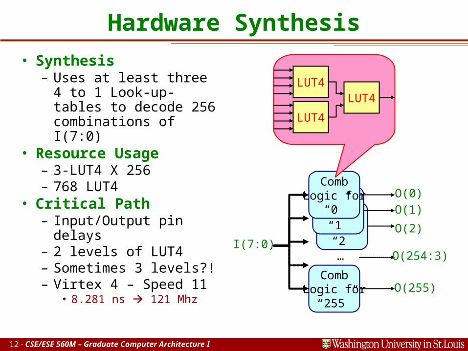
Hardware Synthesis
• Synthesis– Uses at least three 4 to
1 Look-up-tables to decode 256 combinations of I(7:0)
• Resource Usage– 3-LUT4 X 256– 768 LUT4
• Critical Path– Input/Output pin delays– 2 levels of LUT4– Sometimes 3 levels?! – Virtex 4 – Speed 11
• 8.281 ns 121 Mhz
“2”“1”
I(7:0)
CombLogic for
“0”
…
CombLogic for
“255”
O(0)
O(1)
O(2)
O(254:3)
O(255)
LUT4
LUT4
LUT4

13 - CSE/ESE 560M – Graduate Computer Architecture I
Pipelined Decoder• Input/Output pin DFF
– Already in most FPGAs– Minimizes pin latencies
• DFF after every LUT4– LUT4 always followed by DFF
(why not use it)– Only when possible– Minimizes logic latency
• FPGA Resource– 768 LUT4 as before– Plus 768 dff and 264 pin dff– But not really…
• Critical Path– 1 Level of LUT4– Plus small DFF prop delay and
setup– Virtex 4 – Speed 11
• 2.198 ns 455 Mhz• 3.76x Speedup
“2”“1”
I(7:0)
CombLogic for
“0”
…
CombLogic for
“255”
O(0)
O(1)
O(2)
O(254:3)
O(255)
LUT4
LUT4
LUT4
14 - CSE/ESE 560M – Graduate Computer Architecture I
logic
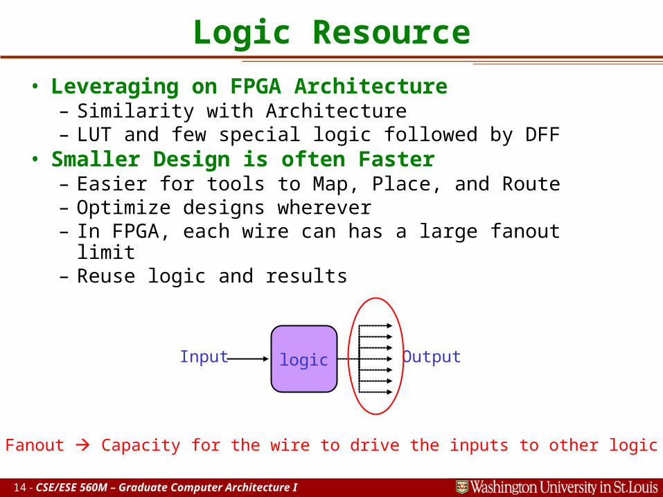
Logic Resource
• Leveraging on FPGA Architecture– Similarity with Architecture– LUT and few special logic followed by DFF
• Smaller Design is often Faster– Easier for tools to Map, Place, and Route– Optimize designs wherever– In FPGA, each wire can has a large fanout limit– Reuse logic and results
Input Output
Fanout Capacity for the wire to drive the inputs to other logic
15 - CSE/ESE 560M – Graduate Computer Architecture I
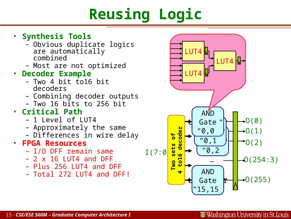
Reusing Logic• Synthesis Tools
– Obvious duplicate logics are automatically combined
– Most are not optimized• Decoder Example
– Two 4 bit to16 bit decoders– Combining decoder outputs– Two 16 bits to 256 bit
• Critical Path– 1 Level of LUT4– Approximately the same– Differences in wire delay
• FPGA Resources– I/O DFF remain same– 2 x 16 LUT4 and DFF– Plus 256 LUT4 and DFF– Total 272 LUT4 and DFF!
“2”“1”
CombLogic for
“0”
…
CombLogic for
“256”
O(0)
O(1)
O(2)
O(254:3)
O(255)
I(7:0) “0,2”“0,1”
ANDGate“0,0”
ANDGate
“15,15”
LUT4
Tw
o s
ets
of
4 to
16 d
eco
der
LUT4
LUT4
16 - CSE/ESE 560M – Graduate Computer Architecture I
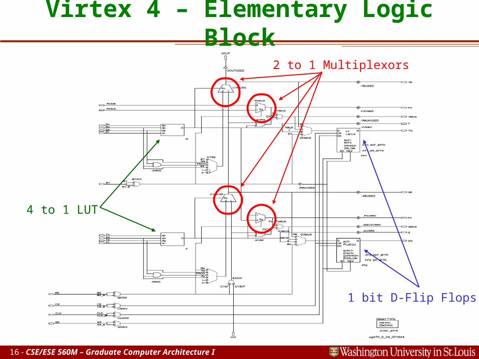
Virtex 4 – Elementary Logic Block
2 to 1 Multiplexors
1 bit D-Flip Flops
4 to 1 LUT

17 - CSE/ESE 560M – Graduate Computer Architecture I
Using MUXF as 2-input Gates
0
a
MUXF0
1sel
b
ab
z z
MUXF0
a
0
1sel
b
ab
Inverters can be pushed into the LUT4 or DFF (by using inverted Q)
zz

18 - CSE/ESE 560M – Graduate Computer Architecture I
Using Unused Multiplexors
• Decoder Example– Replace all LUT4 in
the 2nd Decoder stages with MUX based 2 input AND gates
• Critical Path– Same– 2.198 ns 455 Mhz
• FPGA Resources– I/O DFF remain same– 256 MUXF and DFF– 32 LUT4 and DFF
“2”“1”
CombLogic for
“0”
…
CombLogic for
“256”
O(0)
O(1)
O(2)
O(254:3)
O(255)
I(7:0) “0,2”“0,1”
ANDGate“0,0”
ANDGate
“15,15”
LUT4
Tw
o s
ets
of
4 to
16 d
eco
der
MUXF0
1sel

19 - CSE/ESE 560M – Graduate Computer Architecture I
Parallel Design
• Use Area to Increase Performance– Increase the Input bandwidth (Input Bus width)
• Processing multiple data at a time– Duplicate engines to process independent data sets
• Thread/Object level parallelism• Instructional level parallelism
– Loop unroll to expose the parallelism– Excellent for Streaming Data Applications
• Multimedia• Network Processing
• Performance Scalability– Linear Performance increase with Size
• Achieved for many algorithms– Sometimes Exponential Hardware Size
• Try to scale using higher level of parallelism

20 - CSE/ESE 560M – Graduate Computer Architecture I
Summary• FPGA Designing Methods
– Fine Grain Pipelining to Increase Clock Rate• If possible 1-level of LUT followed by DFF
– Parallel Engines to Increase Bandwidth• Duplicate logic to linearly increase the performance
– Reducing Logic Resource Usage• Reusing duplicate logics• Using all available embedded Logic• There are other logics (i.e. Embedded Procs, Large Memories,
Optimized primitive gates, and IP Cores)• Best Methods Today
– Learn about internal architecture of FPGA– Make your own templates and use them– Use IP Cores
• Future Research Topics– Integration of Generalize Pipelining Algorithms (In the works) – Smarter Synthesis Tools (Understanding HDL)– Automatic Platform Specific Optimization Techniques