general fpga architecture field programmable gate array
TRANSCRIPT


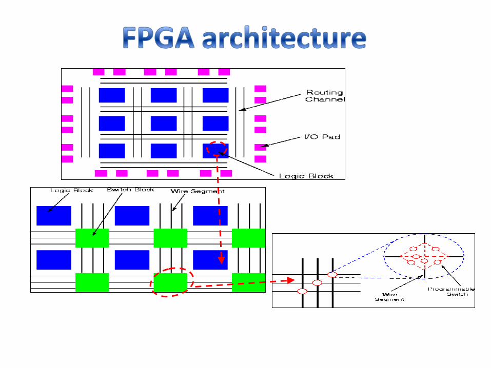
General FPGA Architecture
• Field Programmable Gate Array

Integrated circuit containing many identical logic cells Each logic cell can independently take on one of a
limited set of functions The individual cells are interconnected by a matrix of
wires and programmable switches Larger FPGAs provide additional functional blocks:
Phase-locked loop clock conditioningSerializer/deserializerLarge amounts of on-chip memoryDedicated multiplier/accumulator (“DSP”)
components

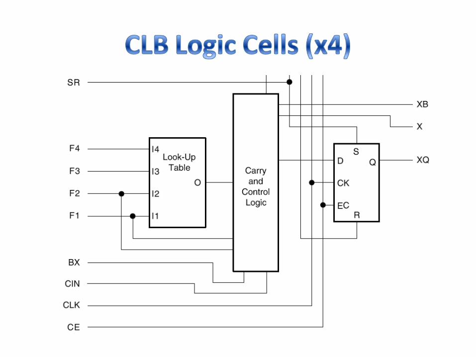

LUT contains Memory Cells to implement small logic functions.
Each cell holds ‘0’ or ‘1’ . Programmed with outputs of Truth Table Inputs select content of one of the cells as output
16-bit SR
flip-flop
clock
muxy
qe
abcd
16x1 RAM
4-inputLUT
clock enable
set/reset
3 Inputs LUT -> 8 Memory Cells
SRAM
Static Random Access MemorySRAM cells
SRAM
3 – 6 Inputs
Multiplexer MUX

SRAM

Connections Routing signals between Logic Blocks. Determined by SRAM cells.
SRAM
Around Fabric Edges Configurable Input Output I/O Blocks100’s – 1,000 Pins
Special Routing for Clocks

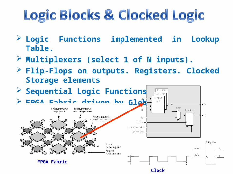
Logic Functions implemented in Lookup Table. Multiplexers (select 1 of N inputs). Flip-Flops on outputs. Registers. Clocked Storage elements Sequential Logic Functions. FPGA Fabric driven by Global Clock.
16-bit SR
flip-flop
clock
muxy
qe
abcd
16x1 RAM
4-inputLUT
clock enable
set/reset
FPGA Fabric
Clock
Integrated circuit containing many identical logic cells.
Each logic cell can independently take on one of a limited set of functions.
The individual cells are interconnected by a matrix of wires and programmable switches.
Larger FPGAs provide additional functional blocks:Phase-locked loop clock conditioningSerializer/deserializerLarge amounts of on-chip memoryDedicated multiplier/accumulator (“DSP”)
components

User provides a hardware description language(HDL).Using electronic design automation tool a technology mapped netlist is generated.Place & route process is done via timing analysis, simulation & other verification method.Then the source file is transferred to FPGA/CPLD via serial interface or to an EEPROM.

SRAM FLOATING GATE FUSE FLASH EPROM

When a customer orders a new type of chip, the manufacturer does not have to design it from scratch, but can just take a standard gate array and modify it to the customer's requirement, because they contain a standard grid of logic gates whose interconnections are specified by the customer.
Can manufacture the first few boards of a new product using FPGAs and then replace with Gate Arrays when the production ramps up.
FPGAs can be programmed on your desktop so fabrication time is not an issue. ----One of the attractions of FPGAs is the ability to prototype very quickly
All components on entire chip can clock at the same time up to hundreds of MHz
FPGAs offer the ability to fix bugs in a design without patching the Printed Circuit Board (PCB). ----Can be a career saver!
The term "field-programmable" may be obscure to some, but the "field" is just an engineering term for the world outside the factory where customers live.
The term "field-programmable" may be obscure to some, but the "field" is just an engineering term for the world outside the factory where customers live.

More expensive than custom siliconSlowerNo dynamic logicNo analog stuff(or small amount of fixed function analog stuff)

DSP Software-defined radio Aerospace Defense system ASIC Prototyping Medical Imaging Speech Recognition Cryptography Bioinformatics

FPGAs bring large amounts of computing power to bear on digital-signal processing problems Scores of computation blocks Fully parallel operation Hundreds of I/O pins
High-level design tools greatly ease the development process. Manufacturer development kits provide a solid foundation for application
development and even production systems. Fast fabrication time and lower cost are the main advantages of gate arrays
over standard cells.It can be programmed instantly using a desktop computer.
The most compelling advantages of FPLDs are low startup cost low financial risk quick manufacturing turnaround easy design changes

Major manufacturers
XILINX & ALTERA
In March 2010, two FPGA companies TABULA & TIER LOGIC announced their new FPGA technology .Tabula uses time-multiplexing and Tier Logic 3D-FPGA technology.
In 1984, Invented by Xilinx co-founder Ross Freeman,the new semiconductor,now known as the field programmable gate array

Digital Circuit and Design by S. Salivahanan & S. Arivazhagan. ISBN 81-259-2063-3.CMOS Digital Integrated Circuit by Sung-Mo Kang & Yusuf Leblebici .ISBN 978-0-07-053077-5.WIKIPEDIA : The Free EncyclopediaXilink Inc.
