what is an fpga a field programmable gate array (fpga) is a semiconductor device containing...
Post on 19-Dec-2015
242 views
TRANSCRIPT
What is an FPGA
• A Field Programmable Gate Array (FPGA) is a semiconductor device containing programmable logic components and programmable interconnects. The programmable logic components can be programmed to duplicate the functionality of basic logic gates such as AND, OR, XOR, NOT or more complex combinatorial functions such as decoders or simple math functions. In most FPGAs, these programmable logic components also include memory elements, which may be simple flip-flops or complete blocks of memory.
• A hierarchy of programmable interconnects allows the logic blocks of an FPGA to be interconnected as needed by the system designer. These logic blocks and interconnects can be programmed after the manufacturing process by the customer so that the FPGA can perform whatever logical function that is needed.
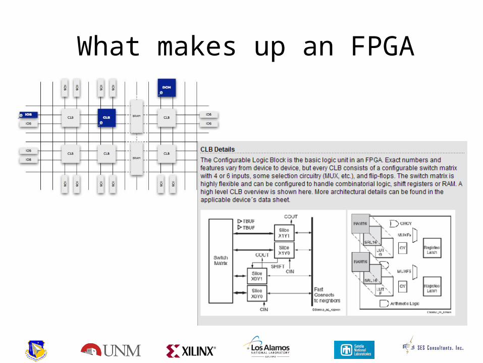
What makes up an FPGA
What projects are FPGAs good for• Aerospace & Defense
Radiation-tolerant FPGAs along with intellectual property for image processing, waveform generation, and partial reconfiguration for SDRs.
• AutomotiveAutomotive silicon and IP solutions for gateway and driver assistance systems, comfort, convenience, and in-vehicle infotainment.
• BroadcastSolutions enabling a vast array of broadcast chain tasks as video and audio finds its way from the studio to production and transmission and then to the consumer.
• ConsumerCost-effective solutions enabling next generation, full-featured consumer applications, such as converged handsets, digital flat panel displays, information appliances, home networking, and residential set top boxes.
• Industrial/Scientific/MedicalIndustry-compliant solutions addressing market-specific needs and challenges in industrial automation, motor control, and high-end medical imaging.
• Storage & ServerData processing solutions for Network Attached Storage (NAS), Storage Area Network (SAN), servers, storage appliances, and more.
• Wireless CommunicationsRF, base band, connectivity, transport and networking solutions for wireless equipment, addressing standards such as WCDMA, HSDPA, WiMAX and others.
• Wired CommunicationsEnd-to-end solutions for the Reprogrammable Networking Linecard Packet Processing, Framer/MAC, serial backplanes, and more
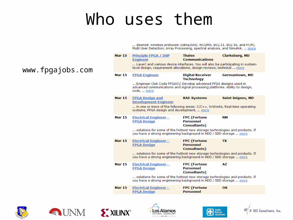
Who uses them
www.fpgajobs.com
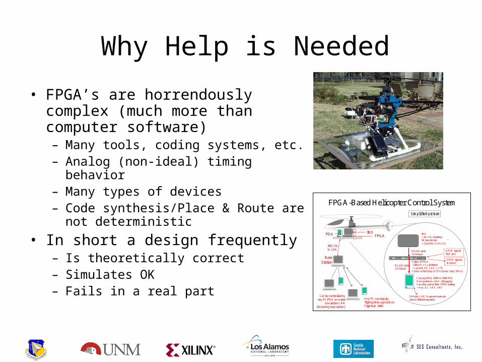
Why Help is Needed
• FPGA’s are horrendously complex (much more than computer software)– Many tools, coding systems, etc.– Analog (non-ideal) timing behavior– Many types of devices– Code synthesis/Place & Route are not
deterministic
• In short a design frequently– Is theoretically correct– Simulates OK– Fails in a real part
FPGA-Based Helicopter Control System
INSFPGAPDA
802.11bWLAN
BaseStation
Can be controlled by any PC/PDA on wired
or wireless LAN(Including base station)
Any PC can display flight path/waypoints on FlightSim 2002
INS2A x 8 v (battery)50 samples/sec2 pounds, 4 x 6 x 2.5”
RS-232 cable115 kbaud
Xilinx II FPGA200 mA x 5 v (battery) 1 pound, 4.5” x 6.5” x 1.75”Closes control loop in 52 microsec (reqt. 20 ms)
RS-232 cable115 kbaud
6 PCM signals from recv
6 PCM signals to servos
5 Mbit WLAN To ground network(about 200kbit required)
Compaq IPAQ 3800 or 3900 PDARuns guidance, comm, debuggingCan draw power from FPGA battery4 oz, 2.5” x 4.5” x 0.5”
Simplified picture
Why are they important
• They have the ability to revolutionize the way that prototyping is done.
• Allows companies to get to market quicker and stay in market longer.
Xilinx
• Largest manufacturer of HW
• Develop hardware and software
• Embedded PowerPC
• SIRF space hardened
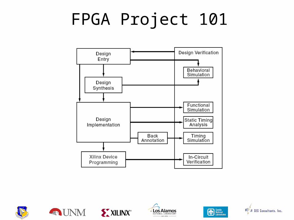
FPGA Project 101
ISE
• ISE is the software used to make the project we are going to complete.
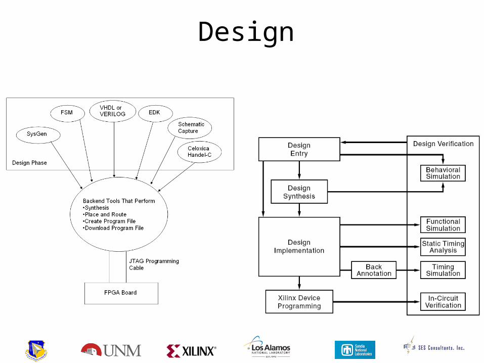
Design
How are FPGAs programs designed
• There are many different methodolgies for programming (or designing) with FPGAs– Hardware Descriptive Language (HDL)
• VHDL• Verilog
– Schematic Capture– C Code– EDK– System Generator
HDLs: VHDL and Verilog
• Hardware Descriptive Languages are ways of describing digital logic. They are not a programming language, they are languages for describing hardware and are the most popular mechanisms for creating FPGA projects– VHDL – VHSIC Hardware Descriptive Language– Verilog
• Which is best?
Schematic Capture
• Could be used– Difficult decission– Not normally used at commercial or university
level for FPGA design
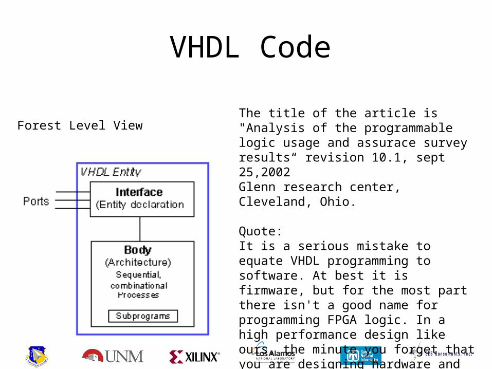
VHDL Code
Forest Level ViewThe title of the article is "Analysis of the programmable logic usage and assurace survey results“ revision 10.1, sept 25,2002Glenn research center, Cleveland, Ohio.
Quote:It is a serious mistake to equate VHDL programming to software. At best it is firmware, but for the most part there isn't a good name for programming FPGA logic. In a high performance design like ours, the minute you forget that you are designing hardware and think you are writing software, you fail.
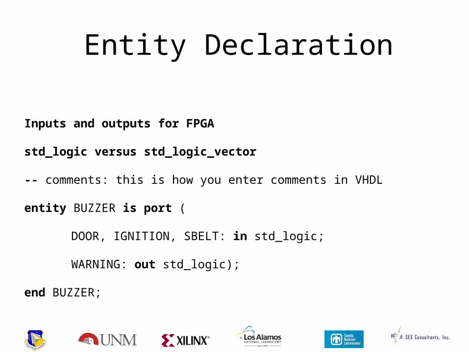
Inputs and outputs for FPGA
std_logic versus std_logic_vector
-- comments: this is how you enter comments in VHDL
entity BUZZER is port (
DOOR, IGNITION, SBELT: in std_logic;
WARNING: out std_logic);
end BUZZER;
Entity Declaration
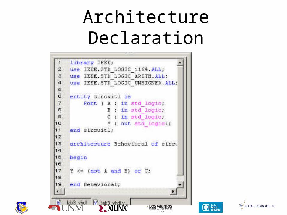
Architecture Declaration
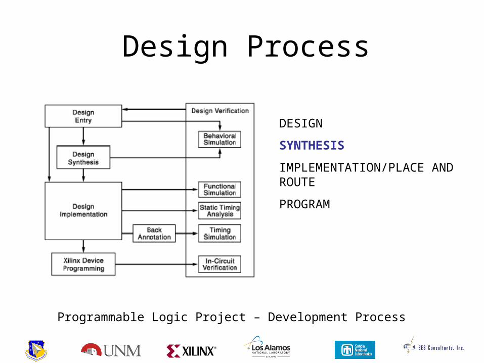
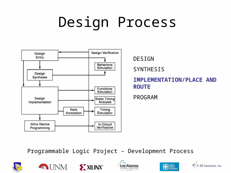
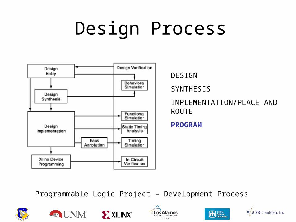
Design Process
Programmable Logic Project – Development Process
DESIGN
SYNTHESIS
IMPLEMENTATION/PLACE AND ROUTE
PROGRAM
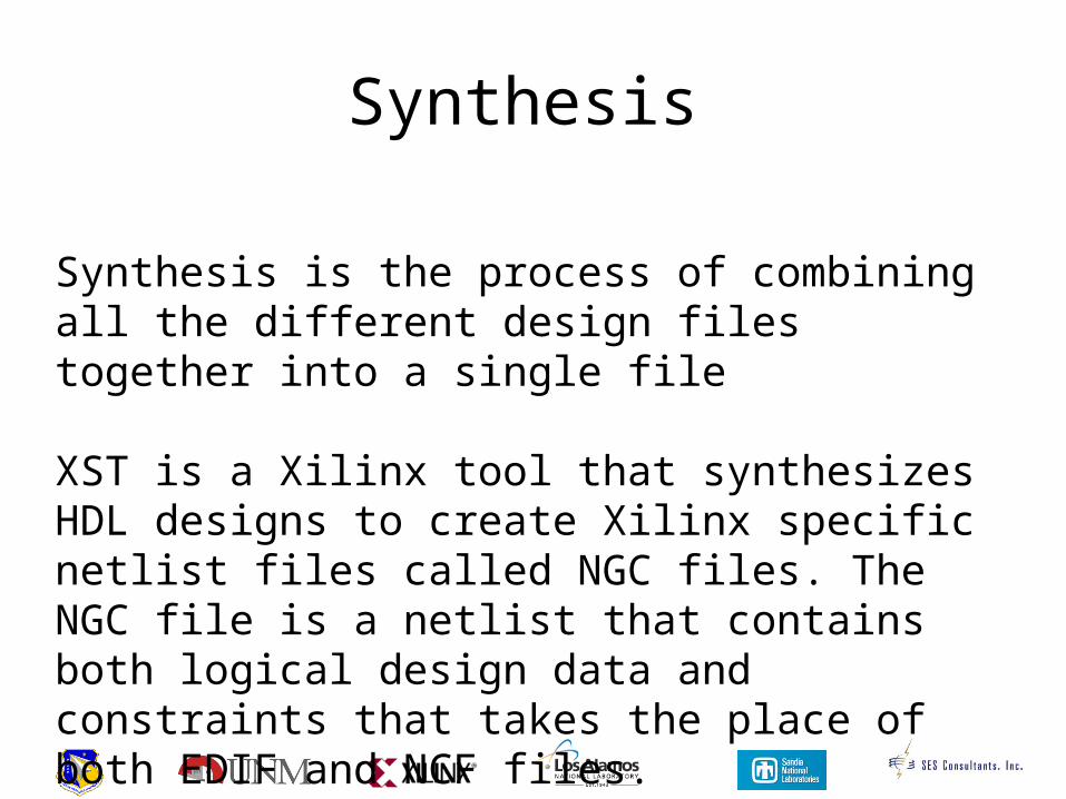
Synthesis
Synthesis is the process of combining all the different design files together into a single file
XST is a Xilinx tool that synthesizes HDL designs to create Xilinx specific netlist files called NGC files. The NGC file is a netlist that contains both logical design data and constraints that takes the place of both EDIF and NCF files.
There are other 3rd party synthesis engines that are very good but not necessary now
Synthesis – Choosing space, speed and other options
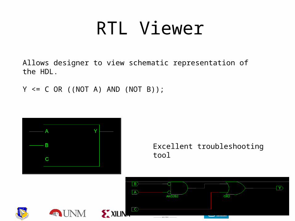
RTL Viewer
Allows designer to view schematic representation of the HDL.
Y <= C OR ((NOT A) AND (NOT B));
Excellent troubleshooting tool
Design Process
Programmable Logic Project – Development Process
DESIGN
SYNTHESIS
IMPLEMENTATION/PLACE AND ROUTE
PROGRAM
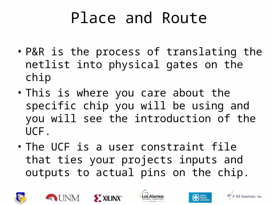
Place and Route
• P&R is the process of translating the netlist into physical gates on the chip
• This is where you care about the specific chip you will be using and you will see the introduction of the UCF.
• The UCF is a user constraint file that ties your projects inputs and outputs to actual pins on the chip.
SynthesisSchematic
Capture
Simulation0 1 0 0 1 1 1 0 1 1 0 0 1 1 1 1
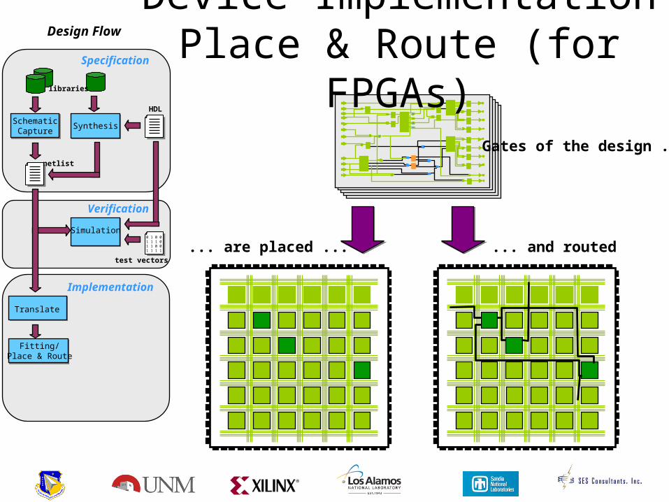
Design Flow
libraries
netlist
HDL
test vectors
Translate
Fitting/Place & Route
Implementation
Specification
Verification
Gates of the design ...
... are placed ... ... and routed
Device ImplementationPlace & Route (for FPGAs)
Design Process
Programmable Logic Project – Development Process
DESIGN
SYNTHESIS
IMPLEMENTATION/PLACE AND ROUTE
PROGRAM
Program the Device
• The FPGA is volatile. There are several ways to program the board– Through the use of the JTAG cable directly– Use the JTAG cable to program memory on the
board and then boot load the FPGA from memory on power cycle
Simulations
• There are two simuators– ISE– Modelsim
• Simulations allow a way to validate your projects. Create modules, test them. Create system, test them.
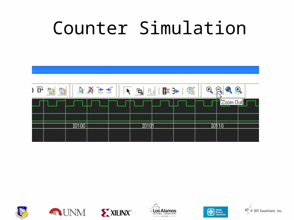
Counter Simulation
Behavioral and Timing Simulation
• There are two main types of simulation that can be performed.
• Behavioral is done to verify the design makes sense – not concerned with specific device parameters
• Functional or timing simulation is performed after the device is mapped to a specific device.
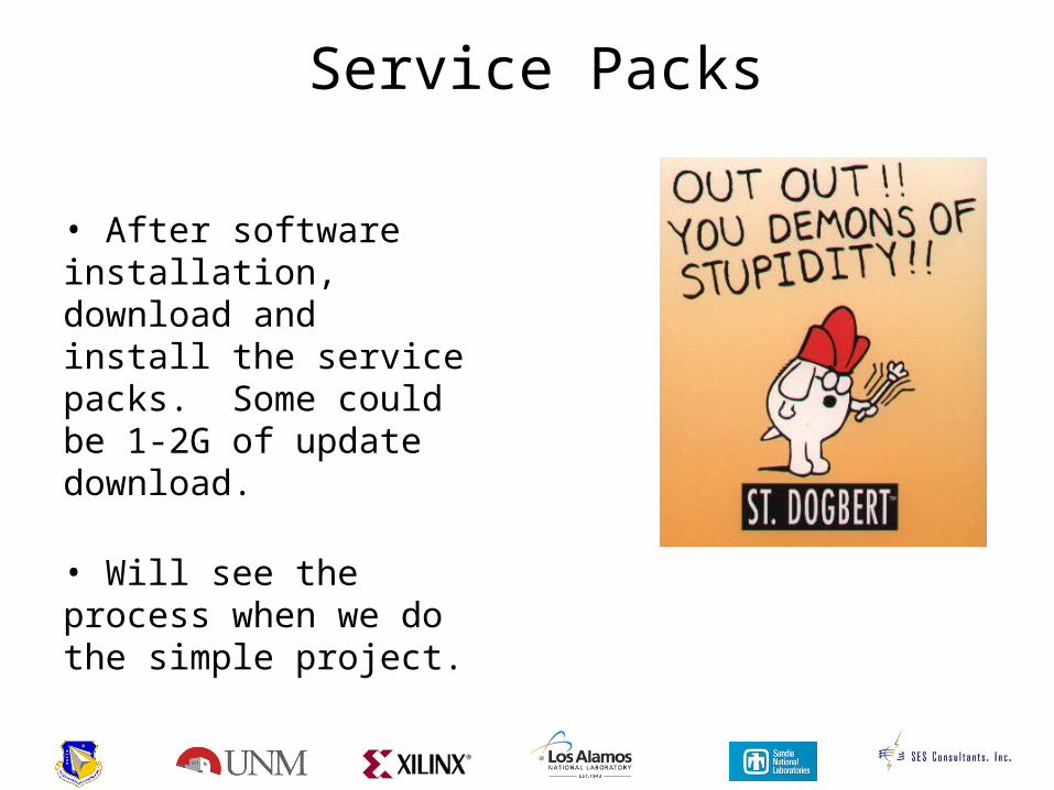
Service Packs
• After software installation, download and install the service packs. Some could be 1-2G of update download.
• Will see the process when we do the simple project.
Default Locations for SW
• When you are setting up the software, regardless of whether it is at the lab or at home, only install the software at the default locations. This is infinitely more critical when you get to a graduate level where you are looking at multiple software packages.
Educational Materials Available
• Clint’s web site www.eecs.wsu.edu/~ee214
• Digilent website www.digilentinc.com
• UNM 238L course site www.ece.unm.edu/vhdl
• XUP site
• www.fpgamac.com (FMAC tutorials used here)
• Quick start tutorials – launch within ISE
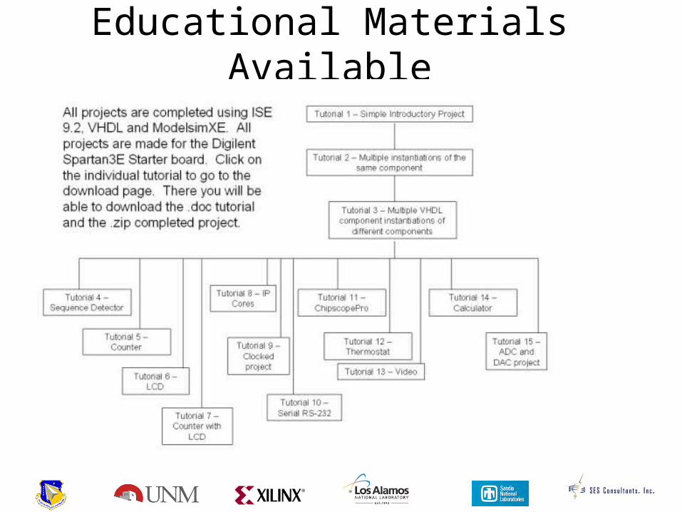
Educational Materials Available
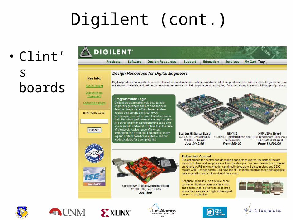
Digilent (cont.)
• Clint’s boards