growth of nickel silicide nanowires by using...
TRANSCRIPT

GROWTH OF NICKEL SILICIDE NANOWIRES BY
USING THERMAL CHEMICAL VAPOR DEPOSITION
FATEMA ABDELLAH AL SALMANI
SUBMITTED TO THE
FACULITY OF SCIENCE
UNIVERSITY OF MALAYA, IN PARTIAL
FULFILMENT OF THE REQUIRMENT FOR THE DEGREE
OF MASTER OF SCIENCE (APPLIYED PHYSICS)
2015

UNIVERSITI MALAYA
PERAKUAN KEASLIAN PENULISAN
Nama: FATEMA ABDELLAH AL SALMANI (No. K.P/Pasport: 02896153)
No. Pendaftaran/Matrik: SGB1300190
Nama Ijazah: SARJANA SAINS (FIZIK GUNAAN)
Tajuk Kertas Projek/Laporan Penyelidikan/Disertasi/Tesis (“Hasil Kerja ini”):
PERTUMBUHAN NIKEL SILISIDA NANO-DAWAI (NiSiNWs) DENGAN
MENGGUNAKAN HABA WAB KIMIA PEMENDAPAN
Bidang Penyelidikan: NANOTEKNOLOGI DAN NANOBAHAN
Saya dengan sesungguhnya dan sebenarnya mengaku bahawa:
(1) Saya adalah satu-satunya pengarang/penulis Hasil Kerja ini;
(2) Hasil Kerja ini adalah asli;
(3) Apa-apa penggunaan mana-mana hasil kerja yang mengandungi hakcipta telah dilakukan
secara urusan yang wajar dan bagi maksud yang dibenarkan dan apa-apa petikan, ekstrak, rujukan
atau pengeluaran semula daripada atau kepada mana-mana hasil kerja yang mengandungi hakcipta
telah dinyatakan dengan sejelasnya dan secukupnya dan satu pengiktirafan tajuk hasil kerja
tersebut dan pengarang/penulisnya telah dilakukan di dalam Hasil Kerja ini;
(4) Saya tidak mempunyai apa-apa pengetahuan sebenar atau patut semunasabahnya tahu bahawa
penghasilan Hasil Kerja ini melanggar suatu hakcipta hasil kerja yang lain;
(5) Saya dengan ini menyerahkan kesemua dan tiap-tiap hak yang terkandung di dalam hakcipta
Hasil Kerja ini kepada Universiti Malaya (“UM”) yang seterusnya mula dari sekarang adalah tuan
punya kepada hakcipta di dalam Hasil Kerja ini dan apa-apa pengeluaran semula atau penggunaan
dalam apa jua bentuk atau dengan apa juga cara sekalipun adalah dilarang tanpa terlebih dahulu
mendapat kebenaran bertulis dari UM;
(6) Saya sedar sepenuhnya sekiranya dalam masa penghasilan Hasil Kerja ini saya telah
melanggar suatu hakcipta hasil kerja yang lain sama ada dengan niat atau sebaliknya, saya boleh
dikenakan tindakan undang-undang atau apa-apa tindakan lain sebagaimana yang diputuskan oleh
UM.
Tandatangan Calon Tarikh
Diperbuat dan sesungguhnya diakui di hadapan,
Tandatangan Saksi Tarikh
Nama:
Jawatan:

UNIVERSITI MALAYA
ORIGINAL LITERARY WORK DECLARATION
Name of Candidate: FATEMA ABDELLAH ALSALMANI
I.C/Passport No: 02896153
Registration/Matric No: SGB130010
Name of Degree: MASTER OF SCIENCE (APPLYIED PHYSICS)
Title of Project Paper/Research Report/Dissertation/Thesis (“this Work”):
"GROWTH OF NICKEL SILICIDE NANOWIRES BY USING THERMAL
CHEMICAL VAPOR DEPOSITION"
Field of Study: NANOTECHNOLOGY AND NANOMATERIAL
I do solemnly and sincerely declare that:
(1) I am the sole author/writer of this Work;
(2) This Work is original;
(3) Any use of any work in which copyright exists was done by way of fair dealing and
for permitted purposes and any excerpt or extract from, or reference to or reproduction of
any copyright work has been disclosed expressly and sufficiently and the title of the Work
and its authorship have been acknowledged in this Work;
(4) I do not have any actual knowledge nor ought I reasonably to know that the making
of this work constitutes an infringement of any copyright work;
(5) I hereby assign all and every rights in the copyright to this Work to the University of
Malaya (“UM”), who henceforth shall be owner of the copyright in this Work and that
any reproduction or use in any form or by any means whatsoever is prohibited without
the written consent of UM having been first had and obtained;
(6) I am fully aware that if in the course of making this Work I have infringed any
copyright whether intentionally or otherwise, I may be subject to legal action or any other
action as may be determined by UM.
Candidate’s Signature Date
Subscribed and solemnly declared before,
Witness’s Signature Date
Name:
Designation:

iii
Abstract
Formation of nickel-silicide nanowires (NiSiNWs) using nickel foil as a catalyst
were studied in this research. The deposition of NiSiNWs was carried out by using home-
built thermal chemical vapor deposition system (CVD). A tungsten filament with purity
of 99.95% was employed as hot-wire for evaporation of Ni catalyst. A silane gas was used
as precursor for the formation of NiSiNWs. The deposition temperature were varied
between 300°C to 577°C and the surface morphology structure, elemental analysis and
crystallinity of NiSiNWs were analyzed on the effect of temperature. The characterization
study was done by using Field emission scanning electron microscope (FESEM), high
resolution transmission electron microscopy (HRTEM), electron diffraction x-ray (EDX)
and X-Ray diffraction (XRD). Moreover, the sample was measured on the electrical
properties by using cyclic voltammetry system. At low temperatures 300°C, 350°C and
393°C, Ni particles only appears on the surface of sample. As temperature increased at
437°C, a little amount of NiSiNWs started to appear on the sample. The appearance of
Ni3Si2 was observed at higher temperatures starting from 477°C. The high density of the
nanowires was demonstrated at high temperatures of 437 ͦ C to 577 ͦ C.
Keywords: nickel silicide, thermal chemical vapor deposition, nanowires, FESEM, XRD.

iv
Abstrak
Pembentukan nikel silicide (NiSiNWs) nanodawai menggunakan kerajang nikel
sebagai pemangkin telah dikaji dalam penyelidikan ini. Pemendapan NiSiNWs telah
dijalankan dengan menggunakan kimia haba wap pemendapan (CVD) system yang telah
dibina sendiri. Satu filamen tungsten dengan ketulenan 99.95% telah digunakan sebagai
wayar pemanas untuk penyejatan Ni pemangkin. Silana gas telah digunakan sebagai
pelopor untuk pembentukan NiSiNWs. Suhu pemendapan telah diubah di antara 300 ° C
hingga 577 ° C dan struktur permukaan morfologi, analisis unsur dan penghabluran
NiSiNWs telah dianalisis berdasarkan kesan suhu. Kajian pencirian dilakukan dengan
menggunakan pelepasan bidang mikroskop elektron imbasan (FESEM), resolusi tinggi
penghantaran elektron mikroskop (HRTEM), elektron pembelauan x-ray (EDX) dan
pembelauan X-Ray (XRD). Selain itu, ciri-ciri elektrik sampel telah diukur dengan
menggunakan sistem kitaran voltammetri. Pada suhu rendah 300 ° C, 350 ° C dan 393 °
C, Ni partikel hanya muncul pada permukaan sampel. Apabila suhu meningkat kepada
437 ° C, sedikit NiSiNWs mulai muncul diatas sampel. Kemunculan Ni3Si2 telah dikesan
pada suhu yang lebih tinggi mulai dari 477 ° C. Ketumpatan tinggi nanodawai telah
ditunjukkan pada suhu tinggi 437 ͦ C hingga 577 C. ͦ
Kata kunci: nikel silicide, menggunakan kimia haba wap pemendapan (CVD), wayar-
nano, FESEM dan XRD.

v
Acknowledgement
I wish to express my great appreciation to Dr. Zarina Binti Aspanut my supervisor for her
supervision and guidance throughout this work. I would also like to express my thanks to
my senior, Mohammad Mukhlis Bin Ramly for his assistance and guidance through the
lab work and analyzing process. And also not forget to thank all LDMRC teams and
students for their cooperation.
I wish to express my deep appreciation to my husband and my children for their
supporting and understanding during the period of my studying.
I would like to thanks my parents and all my family members for their praying and
supporting.

vi
Table of Contents
Page
Abstract ....................................................................................................................... iii
Abstrak ........................................................................................................................ iv
Acknowledgement ........................................................................................................ v
Chapter 1 ...................................................................................................................... 1
INTRODUCTION ........................................................................................................ 1
1.1Importance of Nickel Silicide Nanowires and Applications………………………1
1.2Effect of temperature on material growth techniques……………….. ................... 2
1.3Motivation of this work………. ............................................................................ 3
1.4Objectives…………….. ....................................................................................... 4
1.5Outline of thesis………………. ........................................................................... 4
Chapter 2 ...................................................................................................................... 6
LITERATURE REVIEW .............................................................................................. 6
2.1 Introduction ......................................................................................................... 6
2.2 Nickel Silicide Nanostructures ............................................................................. 6
2.3 Deposition techniques of NiSi Nanostructres ....................................................... 8
2.4 Studies on Surface Morphology and Elemental analysis of NiSi Nanostructures .. 9
2.4.1 FESEM ......................................................................................................... 9
2.4.2 HRTEM ...................................................................................................... 10
2.4.3 EDX ............................................................................................................ 12
2.5 Studies on Structural properties ......................................................................... 14
2.5.1 X-ray diffraction ......................................................................................... 14
2.6 Electrical Measurements .................................................................................... 16
Chapter 3 .................................................................................................................... 17

vii
METHODOLOGY/ EXPERIMENTAL DETALS ...................................................... 17
3.1 Introduction ....................................................................................................... 17
3.2 Thermal Chemical Vapor Deposition System .................................................... 17
3.3 Sample Fabrication ............................................................................................ 21
3.3.1 Substrate Cleaning ...................................................................................... 21
3.3.2 Pre-heating of Filament ............................................................................... 21
3.3.3 Ni Evaporation ............................................................................................ 22
3.3.4 Deposition Process ...................................................................................... 23
3.4 Characterization Techniques and Electrochemical Measurment ......................... 24
Chapter 4 .................................................................................................................... 26
RESULTS AND DISCUSSIONS ............................................................................... 26
4.1 Introduction ....................................................................................................... 26
4.2 Surface and Morphology of NiSi nanostructures ................................................ 26
4.2.1 FESEM Analysis ......................................................................................... 26
4.2.2XRD Analysis .............................................................................................. 31
4.2.3 HRTEM Analysis ........................................................................................ 33
4.3 Electrical Analysis ............................................................................................. 33
4.3.1 CV Measurements ....................................................................................... 33
Chapter 5 .................................................................................................................... 38
CONCLUSION AND SUGGESTION FOR FUTURE WORK ................................... 38
5.1 Conclusion ........................................................................................................ 38
REFERENCES ........................................................................................................... 39

viii
List of Figures
Page
Figure 1 a) Schematic diagram of the main component of FESEM, b)
schematic of signal generated when electron beam strike the
sample (Goldstein et al. 1981), and c) a photograph of FESEM.
11
Figure 2 Schematic representation of an energy-dispersive X-ray
spectrometer (Goldstein et al. 1981).
14
Figure 3 a) Schematic diagram of the X-ray diffractometer, and b) a
photograph of X-ray diffractometer (model of SIEMENS D5000
XRD with thin film attachment operating with CuK radiation).
16
Figure 4 (a) Schematic diagram of Home-built Thermal CVD system. (b) A
photograph of Home-built Thermal CVD system.
21
Figure 5 A photograph of cleaned Ni substrate. 22
Figure 6 (a) Photograph of the setup of the filament, hold by the filament
holder and (b) the pre-heated tungsten coil.
23
Figure 7 Ni evaporation process. 24
Figure 8 Substrate after deposition process. 25
Figure 9 FESEM images of NiSi nanowires prepared by thermal CVD at
different substrate temperatures of (a) 300, (b) 393, (c) 437, (d)
477, (e) 510 and (f) 577◦C.
29
Figure 10 FESEM image of NiSi nanowires with respective EDX spectra
prepared by Thermal CVD at different substrate temperatures of
(a) 393°C, (b) 477°C
31

ix
Figure 11 (a) Dark-field STEM image of NiSi nanowire prepared by Thermal
CVD at substrate temperature of 437◦C, (b–e) EDS element maps
of the nanowire.
32
Figure 12 XRD patterns of NiSi nanowires prepared by Thermal CVD at
different substrate temperature
33
Figure 13 HRTEM image of NiSi nanowires at 437 ͦ C 34
Figure 14 Cyclic voltammetry (CV) curves of NiSiNWs at different scan
rates within a potential window of −0.4 to 0.7 V for different
substrate temperatures.
36
Figure15 Cyclic voltammetry (CV) curves of NiSiNWs at scan rates 5mV/s
within a potential window of −0.4 to 0.7 V for different substrate
temperatures.
37
Figure16 Capacitance and specific capacitance of NiSiNWs at different step
size
38

x
List of Tables
Page
Table 1 ........................................................................................................................ 92

xi
List of Symbols and Abbreviations
CVD chemical vapor deposition
EDX energy-dispersion X-ray spectroscopy
FESEM field emission scanning electron microscope
HRTEM high resolution transmission electron microscopy
Ni nickel
NiSi nickel silicide
NiSiNWs nickel silicide nanowires
sccm standard cubic centimeters per minute
Si silicon
SiH4 silane
SiNWs silicon nanowires
Tf filament temperature
Ts substrate temperature
XRD X-Ray diffraction

xii

1
Chapter 1
INTRODUCTION
1.1 Importance of Nickel Silicide Nanowires and Applications
Nanotechnology is known as the fabrication, design and applications of
nanostructures and nanomaterial. The interest in nanomaterial is mainly due to their
exhibit structural, optical and electrical properties, which are distinctively different from
bulk or even micron-scaled of materials.
Si nanowires (SiNWs) have been widely used in prototype devices such as
integrated electronics, chemical and biological sensors, thermoelectric devices and
lithium ion batteries. To operate these devices efficiently, low resistance contact with the
SiNWs is essential [1]. Metallic silicide nanowires are promising candidates, because
their growth can be easily integrated with silicon processing technology [1]. The synthesis
of single-crystalline, transition metal silicide nanowires, such as TaSi and CoSi has been
recently reported using divers methods. For example, laser ablation [2], chemical vapor
deposition (CVD) [3], and plasma enhanced chemical vapor deposition (PECVD) [4]. As
devices size decreases, the amount of Si consumed in the course of the Si-metal reaction
becomes a major issue, because low Si consumption is crucial to maintain shallow source
and drain junction [2]. Therefore metal silicide that have lower Si consumption are more
desirable. Among all metal silicides, NiSi is superior and convenient due to its lower Si
consumption.
NiSi is an attractive candidate use as a gate contact material due to its low metal-
like resistivity, large processing window (350 ̊C – 750 ̊C) and high temperature stability

2
[5, 6]. Although the NiSi has many phase formations, the predominant phases are Ni2Si,
NiSi and NiSi2. The variation of temperature range during the deposition of Si determines
the phase formation of nickel silicide [7].
NiSiNWs have a high potential in the nanoscale electronics due to the tiny scale
and excellent electrical conductivity [8]. NiSiNWs are considered as potential candidates
to solve the general concerns in terms of electrical resistance and device speed. NiSiNWs
has been intensively researched for use as a contact material of gate and source/drain in
complementary metal oxide-semiconductor (CMOS) devices [9]. NiSiNWs interconnect
has proven a potential to deliver high level current. It also confirmed that each NiSiNWs
delivered current uniformly. Moreover, NiSiNWs has a high advantage to be a field
emitting entity [10].
1.2 Effect of temperature on material growth techniques
The recent studies on NiSiNWs showed that the temperature of substrate for
growing NiSiNWs played a dominant role in controlling the diameter of nanowires and
the formation of various kinds of silicon nanowire-related morphologies [7, 11, 12]. For
example, using HWCVD technique at 400, 450 and 527 ͦ C they obtained the diameters
of about 157,165 and 178nm respectively [13]. Moreover, using simple CVD process a
diameters of 40-60, 100-200 and 100-200nm at 450, 500 and 600 ͦ C were obtained
respectively [14]. The diameters of NiSiNWs increased with increasing substrates
temperatures. The lengths of NiSiNWs varied from tens micrometers to a few hundreds
micrometers as the temperature increased from 450 ͦ C to 500 ͦ C respectively [14].
According to Fan.X.et.al., the morphology and the phase of NiSi can be tuned by
modulating the reaction temperature [14]. Liu, H., et al reported that the amount of Ni
source and the reaction temperature are crucial parameters for the formation of the NiSi
[15].
3
Different phases of NiSiNWs can be formed at different temperatures. For
example, the Ni2Si phase is formed approximately at low temperature range of 250–300 ͦ
C, whereas NiSi2 is formed at temperatures exceeding 800 ͦ C [7].
It has been reported in previous works how the substrate temperatures affect the growth
of NiSiNWs [13, 16]. During the deposition process, a low substrate temperatures from
300 to 393 ͦ C are not sufficient to activate the reaction between Si and Ni to form
NiSiNWs [13, 16], while this formation can be achieved at high temperatures.
In this research the effects of substrate temperatures on the growth of NiSiNWs
will be studied. While fixing other parameters such as the silane flow rate and the
deposition pressure during the experiment.
1.3 Motivation of this work
Considering that the amorphous Si technologies took more than 60 years to mature
and emerge in a variety of electronic applications, however, SiNw technology is still in
its early stage for current technological applications. One of the main reasons is the high
cost of large-scale industrial production. Low temperature and a large area synthesis of
well-aligned SiNWs are the main requirements to satisfy current industrial, scientific and
technological applications of SiNWs. NiSiNWs are expected to further enhance the
properties of the nanowires in their mechanical, chemical resistivity, thermal stability and
in a wide range of optical properties.
Furthermore, highly metallic properties of single crystalline NiSiNWs could be
used as a 1-D electrode to enhance the efficiencies of electron transfer between current
collector support and individual electrode material, and ion transport to the electrode.
Recent studies on the growth of NiSiNWs by thermal CVD demonstrated that it
is a promising technique for the growth of 1-D Si-based nanostructure, owing to the lower
production coasty and the capability for large-scale production making this method more
4
attractive for industrial applications. This technique also have been proven to enhance the
growth rate of NiSiNWs besides have advantages of low-temperature growth processes.
In addition, thermal CVD provides an ion-free deposition by catalytical decomposition of
the source gas using a catalyzer usually tungsten is comparatively a better technique for
the growth of NiSiNWs. Due to the demand from industrial application, the fundamental
study on the effect of substrate temperature by using thermal CVD will be explored in
this research. Moreover, the relation of morphology surface of the sample will be
investigating with the electrical measurement study.
1.4 Objectives
The objectives of this work are as follows:
To growth nickel silicide nanowires by using thermal chemical vapor device
method with nickel as a catalyst.
To investigate the role of substrate temperature on the structural and
morphology of nickel silicide nanowires.
1.5 Outline of thesis
The report is written in five chapters; Introduction on importance of NiSiNWs and
the effect of temperature on material growth technique (Chapter 1), literature review on
NiSi nanostructures, deposition methods and analyses technique (Chapter 2), preparation
of NiSiNWs (Chapter 3), results of each characterization on the NiSiNWs accompanied
by discussion (Chapters 4), and end up with conclusion and suggestions for future works
(Chapter 5).

5
In chapter 1, importance and applications of NiSiNWs are provided. Some of the
synthesis methods are introduced. Moreover, the effects of temperature on material
growth techniques are discussed. The objectives and motivation of this work are
introduced.
In chapter 2, in this chapter literature review of previous works are illustrated.
Some informations about nickel silicide nanostructures are provide and different
deposition techniques of NiSiNWs are discussed. Moreover, studies on surface
morphology and elemental analysis of NiSiNWs are presented.
Chapter 3 will clarify the methodology/experimental details of this research. It
contributes description of home built thermal CVD system used in this work to grow the
nanowires. Moreover, it presents explanations of sample fabrication including the
substrate cleaning process, filament pre-heating, nickel evaporation, deposition process
and characterization techniques.
Chapter 4, in this chapter the effect of substrate temperature on the morphology
and electrical properties of NiSiNWs are explained. The morphology structure of
samples can be view from FESEM and HRTEM images, XRD spectra for crystallinity
and phases, EDX spectra for elemental analysis and cyclic voltammetry curves are
illustrated with related explanations.
Finally, conclusion and suggestions for future work are presented in Chapter 5.
The results and discussion in Chapters 4 aid to build up the conclusive ideas on the
formation of NiSis by employing Ni foil as catalyst and thermal CVD as deposition
technique.

6
Chapter 2
LITERATURE REVIEW
2.1 Introduction
In this chapter a review on nickel silicide nanostructures is presented. Some
deposition techniques are illustrated as well as some characterization techniques.
2.2 Nickel Silicide Nanostructures
Silicide is a compound of Si with an electropositive component [17]. They are
commonly used in silicon-based microelectronics since they can reduce the resistivity of
gate and local interconnect metallization. Some popular silicide candidates, such as CoSi2
and TiSi2, however have some limitations. TiSi2 for example showed line width
dependent sheet resistance and has difficulty in transformation from C49 phase to the low
resistive C54 phase.
Nickel silicides are transition metal silicides with low suitable work functions and
resistivity. They have been applied in several fields [18]. For example, Ni-rich silicides,
such as Ni2Si nanowires, are attractive nanoscale building blocks for interconnects and
fully silicided gate applications in nanoelectronics [19]. Silicon-rich nickel silicide, NiSi2,
has been explored for use in low-power memory devices, and for using an optical absorber
in optical communications applications [20].
Nickel monosilicide (NiSi) is a candidate for deep sub-micron devices due to its
low resistivity, low formation temperature and minimal Si consumption. Nickel disilicide
(NiSi2) is used as a metal base transistor and also finds novel applications as buried

7
epitaxial silicides because of its epitaxial relationship with respect to Si substrate. The
formation of metal silicide film on Si substrate involves diffusion of either the metal or
the silicon species across the interface [21].
Low resistivity, lower Si consumption and lower formation temperatures are some
advantages that present in nickel silicide. It is a promising material to replace those silicde
materials [5].
Recently, Ni silicide has appeared as an ideal electrical contact materials to the
source and provide drain and gate in complementary metal oxide silicon devices. They
also exhibit an excellent scaling down performance [22].
Several NiSiNWs growths have been reported. A unique nanowire growth
mechanism that the NiSi nanowire follows is the metal-induced growth (MIG) method
[17].By sputtering method, the highly linear nanowires were grown by solid-state reaction
of Ni and Si at 575 °C. For applying nanowires as nanoscale interconnections with little
or no damage on the fabricated structures, low-temperature process is desirable. Growing
an epitaxial Si film, which adopts the concepts of solid phase crystallization and solid
phase epitaxy is one of the great advantages of MIG. As a seed layer, the deposited metal
catalyst film, will interacts with sputtered Si to form a silicide layer, which grow Si film
above it. In MIG method, Ni and Co are common metal catalysts. The small lattice
mismatch of CoSi2 or NiSi2 provides an excellent precursor layer to grow an epitaxial Si
film as well as to render a spontaneously formed good ohmic contact layer. MIG method
is a fast Si crystallization method at a low temperature processing and would nurture
versatile approaches in Si application.

8
2.3 Deposition techniques of NiSi Nanostructres
Chemical vapor deposition (CVD) is the oldest techniques in the synthesis of
NiSiNWs. CVD is also known as thermal CVD as it thermally decomposes source gas by
heating. High, moderate and low temperatures CVD are three categories of thermal CVD
according to the deposition temperature.
For high temperature CVD, the reactor is usually constructed by a quartz tube.
Heating element is built outside, surrounding the quartz tube. One end of the tube supplies
Si-containing vapor, the other end is connected to evacuation tools.
Moderate temperature CVD typically works at a temperature range from 400
to700 ͦ C. It is constructed by a stainless steel or quartz-made reactor, with heating element
built inside the reactor. Different from high temperature CVD, only substrate rather than
the reactor is heated up.
In moderate and low temperature CVD, SiH4 is frequently used as precursor while
in high temperature SiCl4 is used.
The decomposition process can be presented by the following equation:
SiH4 (g) SiH2 (g) + H2 (g)
However, a higher temperature (~ 600 ̊C) is required for decomposition of SiH4 gas. Thus,
the better quality, less kinking and defects SiNWs are mostly synthesized at temperatures
beyond 500 ̊C.
The most important advantages of thermal CVD are the broader choice of catalyst
and allowing epitaxial growth of SiNWs. The wide range of operating temperature
permits a large variety of metals to be involved in growth. For example Au, Al, Ag, Cu
and Ni.
Thermal chemical vapor deposition (CVD) considered as low temperature CVD
technique. It utilizes a metallic catalyzer to decompose SiH4 precursor. Thermal CVD is

9
constructed by tungsten filament coil served as a catalyzer. It is connected to a high
voltage power source which supplies power to heat up the filament for deposition.
2.4 Studies on Surface Morphology and Elemental analysis of NiSi Nanostructures
2.4.1 FESEM
The characterization on NiSi nanostructure is highly dependent on surface morphological
imaging technique. An optical microscope is no longer applicable in order to view
submicron to nanosize of structures due to the resolution limit. For better resolution and
depth of focus electron microscope is needed, due to the natural behavior of electron
compared to photon [23].
FESEM is commonly used to study the surface morphology of the nanostructure
materials. In this device the electron source is produced by field emission gun. It can
achieve up to three orders of magnitude greater electron density and higher brightness.
The main components of FESEM, the signal generated when electron beam strike the
sample and a photograph of FESEM instrument are shown in Figure1 (a), (b) and (c)
respectively. Electrons are liberated from a field emission source and accelerated in a high
electrical field gradient. Within the high vacuum column these so-called primary electrons
are focused and deflected by electronic lenses to produce a narrow scan beam that
bombards the object. As a result the "electron hail" secondary electrons are dislocated
from each spot on the object. The smaller the angle of incidence of the electron beam is
with respect to the sample surface and the higher a certain point is in the sample, the more
secondary electrons are able to reach the detector and the lighter this dot will appear in
the final image following electronic signal amplification and digitalization.

10
2.4.2 HRTEM
Transmission electron microscopy (TEM) plays an important role for the
characterization of the structural properties and crystallinity of the SiNWs. Atomic
structure of a SiNWs can be directly investigated by employing high resolution
transmission electron microscopy (HRTEM). A high resolution of ~1 Å is theoretically
obtained in a HRTEM due to the shortening in de Broglie wavelength of the high energetic
electron beam [23]. This is useful in determination of the crystalline or amorphous
structures and structure defects such as twinning and lattice dislocation within NWs. It
can also be used to identify the atomic lattice spacing, crystalline plane, preferred
orientation and growth direction of the NWs.
(a) (b)
(c
)
Figure 1: a) schematic diagrame of main componant of FESEM, b) schematic of
signal generated when electron beam strike the sample (Goldstein et al. 1981), and
c) a photograph of FESEM

11
TEM is constructed with an electron gun, usually field emission gun for high
resolution. The voltage applied to accelerate the electron is in a range of 200 to 300 kV
to allow the transmission of electron beam through the specimen. The electron beam is
focused by two condenser lenses into a coherent beam, and further restricted from
deviation by a condenser aperture. The focused electron beams then strike the specimen
and are transmitted through the specimen. The transmitted electrons are focused by the
objective lens into an image which is then passed through the intermediate and projector
lenses, and then projected on the fluorescent screen. The objective and selected area
apertures are used for TEM image and diffraction pattern projections, respectively. For
the TEM image projection mode, the objective aperture acts to block the high angle
diffracted electrons, while, for the diffraction pattern projection mode, the selected area
aperture acts to assist the examination of the diffraction of electrons. The transmitted
electrons can be classified into three types, namely unscattered, elastically scattered and
inelastically scattered electrons. The electrons transmitted through the specimen without
any interaction with the specimen atoms are called unscattered electrons. These
unscattered electrons mainly contribute to the TEM images.
The darker area in a TEM image can be due to the thicker or heavier element in
that area, thus fewer electrons are transmitted through that area. Elastically scattered
electrons are generated when the incident electrons are scattered by the specimen atoms
with no loss of energy. The elastically scattered electrons follow Bragg’s diffraction law,
where the incident electrons are scattered by the atoms with the same atomic spacing and
possess same scattering angle. The same angle of scattered electrons forms a pattern of
diffraction spots. This diffraction pattern is utilized to generate selected area electron
diffraction (SAED) pattern, which gives information on the structures (amorphous or
crystalline), orientation and atomic arrangement of the sample. Conversely, the electrons
generated when the incident electrons interact with the specimen atoms with loss in

12
energy are inelastically scattered electrons. The inelastic loss of energy by the incident
electrons is unique to each of the elements interacted with. Thus, it provides the
information of the compositional and chemical bonding of the sample.
In order to obtain higher resolution (up to atomic level), the sample should be thin
enough (< 100 nm) to enable the transmission of the electron beam. A TEM grid, usually
copper grid with carbon supporting film, is used to hold the sample. The samples on the
substrate were immersed in an ethanol solution and sonicated for about 15 minutes to
extract the SiNWs from the substrate. The diluted SiNWs in an ethanol solution was then
transferred onto a copper grid through a cleaned pipette. The copper grid was dried in a
dry cabinet for a few hours before carrying out TEM measurement.
2.4.3 EDX
Energy dispersion X-ray spectroscopy EDX provides a qualitative and
quantitative analysis of the chemical composition of the NiSiNWs sample. The detector
can be attached in a FESEM or HRTEM to effectively collect the X-ray radiation from
the sample. The radiated X-ray at all energies is collected at the same time while a
complete spectrum covering the whole energy range can be acquired for analysis using
EDX.
A schematic diagram of an EDX is illustrated in Figure 2 [24].Generally, an EDX
consists of a detector, an amplifier and a multichannel analyzer. The detector is
constructed by a small piece of semiconductor plate, usually Si or germanium (Ge), with
a p-i-n junction in reverse biased. The Si is doped with Li and cooled down to ~77 K with
liquid N2 to increase the resistivity of the Si plate, thus limits the current leaking through
when voltage is applied through the Si plate. Both sides of the Si plate are covered by thin
layers of Au electrodes (~20 nm) so that bias voltage can be applied through the p-i-n
junction of Si. A thin beryllium window is placed in the outer surface of the detector to

13
prevent contaminants coating the detector. As a result, EDX is not able to detect all
elements lighter than sodium (Na) because the X-rays radiated by those light elements are
not able to transmit through the beryllium window of the detector. However, utilization
of Polymer-based thin windows allows for detection of light elements.
Figure 2: schematic representation of an energy-dispersive X-ray
spectrometer (Goldstein et al. 1981).

14
2.5 Studies on Structural properties
2.5.1 X-ray diffraction
X-ray diffraction (XRD) is commonly used in characterization of the crystal
structure of a material. Crystallinity of an element can be identify by determining the peak
position in XRD spectra, while the orientation plane correspond to the peak can be
assigned.
The XRD spectrum provides a qualitative determination of the crystallinity of a
material by analyzing the intensity of the diffraction peak. Crystallite size of the material
can be quantitatively calculated from the width of the diffraction peak using several
methods.
As XRD detector is only sensitive to crystalline structures, it can be applied for
both homogeneous and inhomogeneous samples, which is suitable for the structural
characterization of nanomaterials.
A schematic diagram and a photograph of X-ray diffractometer are illustrated in
Figure 3 (a) and (b) respectively. The diffractometer is designed according to the Bragg-
Brentano geometry. It consists of a monochromatic X-ray radiator and a detector, which
are placed on the circumference of a circle centered on the sample. X-rays are generated
in a cathode ray tube by accelerating electron towards a Cu anode plate. CuKα is
commonly used as X-ray source. The produced X-ray beam is then filtered by
monochromator to a wavelength of 0.7 to 2 A and collimated towards sample. The X-ray
beam diverges from the source and diffracted by the sample to form a convergent
diffracted beam. The convergent diffracted beam is filtered by a monochromator and
focused at a slit, then enters the detector. Intensity of the diffracted X-ray beam is
measured as the number of current pulses per unit time by an electronic X-ray detector.
During the measurement, the X-ray detector is mechanically rotated in an angle of 2θ

15
accompanied by a rotation of sample holder in an angle of θ, while the angle of incident
beam to sample holder always keeps at θ. Thus, the angle of incident beam is always equal
to the angle of diffracted beam.
The detector measures data of each angular increment in a minimum order of
0.01o, while the length of time per count and step size of the angular increment are
controlled by the computerized program.
When Bragg’s law is satisfied in measuring a crystalline sample, the X-rays
scattered by all the atoms in all of the planes are completely in phase, thereby forming
constructive interference and the X-rays are diffracted at maximum intensity. This results
in the diffraction peak in XRD pattern. The intensity of the diffraction peak is proportional
to the degree of crystallinity of the sample. In the rest of angles, the scattered rays cancel
out each other (destructive interference).
K filter
2 Sample
Detector
diaphragm
Detector
Aperture
diaphragm
Measuring circle
Focusing circle
Scattered-
radiation
diaphragm
Focus
X-ray tube
θ Glancing angle
2θ Diffraction angle
α Aperture angle
Figure 3: a) schematic diagram of the X-ray diffractometer, and b) a photograph of X-ray
diffractometer (model of SIEMENS D5000 XRD with thin film attachment operating with CuK
radiation)

16
2.6 Electrical Measurements
The electrochemical measurements were carried using a three-electrode
configuration in 0.5M Na2SO4 electrolyte. NiSiNWs used directly as a working electrode
with Pt and SCE as the counter and references electrode respectively. CV operation was
conducted to evaluate the electrochemical performance of the samples. The specific
capacitance was calculated from the CV curve using equation 1:
𝐶 =1
𝑚 𝜈 𝛥𝑉 ∫ 𝑖 𝑉 𝑑𝑉 (1)
Where C is the specific capacitance, m is the mass of the active materials in the
electrode, 𝜈 is the potential scan rate, Δ𝑉 is the potential window in the CV and ∫ 𝑖 𝑉 𝑑𝑉
is the integrated area of the CV curve.

17
Chapter 3
METHODOLOGY/ EXPERIMENTAL DETALS
3.1 Introduction
In this chapter, setup for the home-built thermal CVD is presented. Sample
fabrication is explained by illustrating the substrate cleaning, filament pre-heating, and
nickel evaporation and deposition process respectively. Information about
characterization techniques are included at the end of this chapter.
3.2 Thermal Chemical Vapor Deposition System
A schematic diagram and a photograph of the home-built thermal CVD system is
illustrated in Figure 4 (a) and (b) respectively. The system consists of six parts; the CVD
reactor, plasma generator, hot-wire power supply, vacuum system, gas line management
and heating elements.
The CVD reactor of this deposition system consists of a cylindrical stainless steel
chamber. The CVD reactor is well-sealed with Viton o-rings and is directly connected to
a vacuum pump for evacuation. The connecting tube has an air admittance valve for
venting purposes. A glass viewport on the body of the reactor is used for viewing interior
of the reactor. It also acts as a window for the optical pyrometer used to determine the
filament temperature. A stainless steel made substrate holder is designed to hold
substrates with dimensions of 2.5 x 2.5 cm. The heater rod and thermocouple are attached
to the substrate holder which is grounded to the earth and isolated from the body of the
reactor by Quartz stands.

18
Tungsten wire (purity of 99.95 %) is coiled to form a solenoid shaped filament
with ~30 coils of diameter 2 mm and length of ~2 cm. This filament coil serves as the hot
filament for the evaporation of metal catalyst and decomposition of source gas. The
tungsten filament is placed on a filament holder, which is connected to a power supply.
The power supply consists of a voltage regulator (IBC voltage regulator 1P-1kVA) with
voltage ranging from 0 – 250 V and a step down transformer. The transformer steps down
the output voltage to a range of 0 – 20 V and maximum current of 60 A. By regulating
the voltage supplied to the tungsten filament, different filament temperatures, Tf can be
controlled for deposition. An ammeter is connected with the voltage supply to measure
the current flow through the tungsten filament. Tf is measured by a pyrometer (Reytek,
Raynger, 3i). The detector of the pyrometer is stimulated by the incoming infrared energy
and produces a signal to the circuitry, which will process the signal and compute the Tf.
The tungsten filament is pre-heated to remove surface contaminations such as carbon and
other metallic elements before deposition. Pre-heat treatment is carried out for 10 minutes
at Tf ~1600 °C in H2 with flow rate of 100 sccm.
For the purpose of materials fabrication in CVD, a high vacuum level is important
to provide a clean deposition environment and minimize contaminations in the sample. A
vacuum pump is a device that removes gas molecules from a sealed volume in order to
leave behind partial vacuum. A rotary pump is to expand the volume of a container. To
continue evacuating a chamber indefinitely without requiring infinite growth, a
compartment of the vacuum can be repeatedly closed off, exhausted, and expanded again.
The simplest rotary pump is a circular rotor rotating inside of a larger circular cavity. The
centers of these two circles are offset, causing eccentricity. The vanes are allowed to slide
into and out of the rotor and seal on all edges, creating vane chambers that do the pumping
work. On the intake side of the pump, the vane chambers are increasing in volume and
are filled with fluid forced in by the inlet pressure. On the discharge side of the pump, the

19
vane chambers are decreasing in volume, forcing fluid out of the pump. The rotary
vacuum pumps can attain pressures as low as 10-3 mbar.
A highly purified SiH4 (99.9995%) is used as the precursor gas and H2 gas with
purity of 99.999% is used to dilute the SiH4 gas in deposition, it's also serves as a precursor
in pre-heating of coiled tungsten filament process.
The source gas tanks are stored in a gas room. The SiH4 gas tank is kept in a
secured gas cabinet equipped with a control panel. The source gases are introduced into
the CVD reactor through the gas line, which is constructed using a 316L stainless steel
tubing (outside diameter of 1/4 in). A check valve is installed in each gas line to prevent
the backflow of the source gas. A ball valves are used to open or close the gas line, while
metering valves are used to roughly control the amount of gas flow. The gas flow rate is
accurately controlled by using a mass flow controller (MFC) with unit reading of standard
cubic centimeters per minute (sccm). The SiH4 and H2 gas flow rate are controlled by a
MFC in a flow rate range of 0 – 10 sccm and 0-200 sccm respectively.

20
(a)
(b)
Figure 4: (a) Schematic diagram of Home-built thermal CVD
system. (b) A photograph of Home-built thermal CVD system.
View portHot filament
RF electrode
Substrate holder
Electrical feedthrough
(Heater & Thermocuople)
High Current SupplyGauge
To RF supplyGases inlet
To vacuum system
View portHot filament
RF electrode
Substrate holder
Electrical feedthrough
(Heater & Thermocuople)
High Current SupplyGauge
To RF supplyGases inlet
To vacuum system

21
3.3 Sample Fabrication
3.3.1 Substrate Cleaning
Prior to the substrate cleaning, the tools such as tweezers, petri disc and beakers
were cleaned using acetone and dried under N2 purging. A Ni substrates were cleaned
using deionized water and acetone. First, Ni foil substrate were immersed in a beaker
containing deionized water. Then, Ni foil substrates were immersed in a beaker containing
acetone. This step was repeated for two times to remove organic impurities. The Ni foil
cleaning process was ended with purging N2 gas on the sample. A cleaned Ni foil substrate
is shown in Figure 5.
3.3.2 Pre-heating of Filament
The tungsten filament was pre-heated to remove surface contaminations such as
carbon and other metallic elements before deposition. Pre-heat treatment was carried out
for 10 minutes at Tf ~1600 °C in H2 with flow rate of 100 sccm. Both for Ni evaporation
and deposition process required a pre-heated tungsten filament. The setup of the filament,
Figure 5: A photograph of cleaned Ni Foil
substrate.

22
hold by the filament holder and the pre-heated tungsten coil are shown in Figure 6 (a) and
(b) respectively.
(a)
(b)
3.3.3 Ni Evaporation
Figure 7 illustrates a photograph of CVD system during Ni evaporation process.
Samples were prepared by Ni evaporation using heated tungsten filament. Ni foil with
1mm width and 12mm length (1 mm x 12 mm) which was tightly hung on a coiled
filament is used as a source of evaporation. The Ni was evaporated at a filament
Figure 6: (a) photograph of the setup of the filament,
hold by the filament holder and (b) the pre-heated
tungsten coil.

23
temperature ~ 1600 °C in a H2 flow rates of 100 sccm on a heated substrate temperature
of 150 °C. The hot wire voltage supply used for Ni evaporation was 150 V. The
evaporation time was fixed at 5 minutes.
3.3.4 Deposition Process
Deposition process is accomplished by the decomposition of silane gas on Ni
surfaces to make different composition (NiSi, Ni2Si, and Ni3Si2) of nanowires[9].
Deposition process was carried out by varying the substrate temperature from
300°C to 577°C. The SiH4 and H2 gas flow rate were fixed at 7sccm, 100sccm
respectively. The chamber pressure was fixed at 0.5 mbar. The filament to substrate
distance was fixed at 2.5 cm. The deposition time was fixed 5 minutes. A photograph of
substrates after deposition process is shown in Figure 8.
Figure 7: Ni evaporation process

24
3.4 Characterization Techniques and Electrochemical Measurment
The morphological study for the FESEM images of the nanowires were obtained
using a (JEOL- JSM 7600-F) at low electron accelerating voltage of 2 kV. While the
elemental analysis for the EDX spectrum was collected by (JEOL- JSM 7600-F). The
working distances for the imaging and EDX were fixed at 8 mm and 15 mm respectively.
Nanostructure analysis for the HRTEM image of the nanowires were obtained byTEM
(JEOL JEM-2100F) with an accelerating voltage of 200 kV. The crystalline orientation
for the X-ray diffractometry (XRD) spectra were recorded in the 2 range of 20–70◦ at a
fixed grazing incidence angle of 1.5◦ using a PAN-alytical Empyrean X-ray
diffractometer with X-ray wavelength of 1.5406 ˚A. The step time and step size of the
scanning were fixed at 2 s and 0.026◦, respectively. The XRD was the most widely used
technique in materials characterization, which is based on the diffraction of X-ray
radiation within the film structure.
Figure 8: substrate after deposition process

25
The electrochemical measurements were carried using a three-electrode
configuration in 1M KOH as electrolyte. NiSiNWs used directly as a working electrode
with Pt and Hg/HgO as the counter and references electrode respectively.

26
Chapter 4
RESULTS AND DISCUSSIONS
4.1 Introduction
This chapter presents the results and discussions involved in this study on the
growth of NiSiNWs using nickel as a catalyst by thermal chemical vapor deposition
(CVD). The results obtained from Field emission scanning electron microscopy
(FESEM), X-ray diffractometr (XRD), high resolution transmission electron microscopy
(HRTEM) and electrical analysis are presented in different subsections of this chapter.
4.2 Surface and Morphology of NiSi nanostructures
4.2.1 FESEM Analysis
FESEM images of NiSiNWs prepared by thermal CVD at different substrate
temperatures are presented in Figure 9. The sample prepared at 300°C showed a formation
of spherical grains of Ni nanoparticles distributed on the substrate surface. At this low
substrate temperatures, SiH4 and Ni catalyzed decomposition are not sufficient to form
NiSi particles during the reaction [5]. The reaction of Ni and Si most probably occur on
the Ni nanoparticles surface only. Therefore, no nanowires formed at this low temperature
due to the insufficiency of Si to Ni ratio for achieving its nucleation [13]. As the
temperatures increased to 437 °C short nanowires started to grow on the roots and
randomly distributed on the surface of the substrate. This could be due to the low substrate
temperature attributed to a low surface mobility for forming NiSi solid particles. Further
increasing in the temperatures result in randomly growth and few nanowires grown on

27
the same root as demonstrated in Figure 9 at 477°C. The moderate mobility of the growth
species at this temperature are sufficiently enhances the formation of NiSi phase solid
particles and increase the precipitation of the nanowires. At temperatures of 577°C the
roots are still observed and higher density, longer nanowires are appeared. The
decomposition of SiH4 and Ni diffusion at this temperature is sufficient as a result the
reaction forms different phases of NiSi and the nanowires formed are higher density and
longer comparing with those formed at lower temperatures. From the insert image of
Figure 9 (d-f), it is observed that more than one nanowire are grown from one root. The
average estimated length of the nanowires prepared at 437, 477, 510 and 577°C are about
179.3nm, 436.5nm, 580.8nm and 853.6nm respectively. While the average estimated
width of the nanowires roots at these temperatures are 43.4nm, 124.1nm, 345.4nm and
529.8nm respectively. This increase in the nanowires density is similar to several reported
works previously [11, 12]. It is believed that this increase in nanowires' lengths and roots'
widths is due to the increase in surface mobility of the growth species [13]. It is also
depend on the diffusion rate of Ni and Si in the CVD chamber. At high temperatures the
diffusion of Si increased and this give rise to the formation of NiSi at different phases.
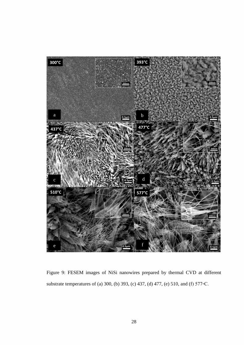
28
Figure 9: FESEM images of NiSi nanowires prepared by thermal CVD at different
substrate temperatures of (a) 300, (b) 393, (c) 437, (d) 477, (e) 510, and (f) 577◦C.
200nm
577°C
200nm
510°C
0.5µm
0.5µm
200nm
477°C
200nm
437°C
0.5µm
200nm
393°C
0.5µm
300°C
200nm
a b
c d
e f

29
The FESEM images of the samples prepared at substrates temperatures 393°C and
477°C with respective EDX spectra are shown in Figure 10. The elemental composition
of the samples at 393°C and 477°C are tabulated in table 1. It is noticed that at 393°C the
sample consist of 89.17% Ni, 9.41% Si and 1.42% O. At this temperature Ni is dominant
because the diffusion rate of Ni is faster than Si. However, the NiSi is not observed in
XRD spectra in Figure 12 at 393°C. This is because the amount of Si is not sufficient
enough to form nanowires.
At 477°C the percentage of Ni, Si and O are 80.72%, 18.06% and 1.22%
respectively. As the temperature increased the diffusion of Si increased and this give rise
to the formation of NiSi at different phases. The Ni to Si ratio at 393°C and 477°C can be
calculated from table 1 and they are 9.48 and 4.47 respectively.
Table 1
Element contents of NiSi nanowires at 393 °C and 477 °C
Temperatures
(°C )
Ni (%) Si (%) O (%) Ni to Si ratio
393 89.17 9.41 1.42 9.48
477 80.72 18.06 1.22 4.47

30
Figure11 illustrated the composition of NiSiNWs investigated by STEM/EDS
elemental mapping at 437. As Figure11 (a) shows a typical bright-field STEM image of
a single nanowire on a carbon film supported by a TEM copper-grid clearly reveals that
the nanowire consisted of a core only without a shell. The Ni, Si, C and O elemental maps
of the nanowires are presented in Figure11 (b), (c), (d) and (e) respectively. From the
elemental mapping result it is observed that the nanowires consist of Ni and Si only. The
appearance of O generally occurs in CVD grown nanowires it might originate from
residual air inside the chamber. While the C come from the carbon film supported by
TEM copper- grid.
(a) (b)
Figure 10: FESEM image of NiSi nanowires with respective EDX spectra
prepared by thermal CVD at different substrate temperatures of (a) 393°C, (b)
477°C.

31
4.2.2XRD Analysis
The XRD pattern of NiSiNWs prepared at different substrate temperatures are
shown in Figure 12. At low temperatures 300°C and 393°C, Ni only appears in the surface
of the sample. It is located at 44.50 ͦ and 76.37 ͦ belongs to the (111) and (220) crystalline
planes according to the JCPDS card number 00-004-0850. At these low temperatures, the
arrival of Si- rich species on the Ni surface is not sufficient to activate the reaction of Ni
and Si or the formation of NiSi is very low through the solid diffusion control process
described by Peng et al [7, 13, 25]. This observation support the FESEM images in Figure
9 a, b and c in which no NiSiNWs observed.
As the temperature increased at 437°C, a little amount of NiSi located at 47.28 ͦ
belongs to the (202) crystalline planes according to the JCPDS card number 00-038-0844
started to appears in the sample. The appearance of Ni3Si2 is observed at higher
temperatures starting from 477°C. And it is located at 46.74 ͦ belongs to the (531)
Figure 11: (a) Dark-field STEM image of NiSi nanowire prepared by thermal CVD at
substrate temperature of 437◦C, (b–e) EDS element maps of the nanowire.

32
crystalline planes according to the JCPDS card number 00-017-0881. These results
support the previous discussed FESEM images where the nanowires can be seen clearly
on the surface of the samples prepared at higher substrate temperatures 437, 477, 510 and
577°C. The increase in the temperature leads to transition of Ni-rich silicide to Si-rich
silicide. And different silicide phases to appear such as NiSi and Ni3Si2.
Figure 12: XRD patterns of NiSi nanowires prepared by thermal CVD at different
substrate temperature
20 30 40 50 60 70 80
0
1000
2000
3000
4000
5000
6000
7000
8000
9000
10000
Ni
NiSi
Ni3Si
2
577C
510C
477C
437C
Inte
nsity (
arb
.units)
2()
393C
20 30 40 50 60 70 80
0
2000
4000
6000
8000
10000
12000
14000
16000
18000
Ni
350C
300C
2()
Inte
nsity (
arb
.un
its)

33
4.2.3 HRTEM Analysis
The microstructure of these nanowires was investigated by HRTEM as
shown in Figure 13. A single nanowire of the sample prepared at 437 ͦ C was
selected for this HRTEM measurement. From the image it is clear that the NiSi
nanowires consist no shell but only core. The elemental composition contents Si
and Ni as discussed previously. The estimated lattice spacing is about 0.19 nm
corresponds to NiSi (202) crystallographic plane JCPDS card No. 00-038-0844
which agreed with XRD spectra of 437 ͦ C as reported above.
4.3 Electrical Analysis
4.3.1 CV Measurements
Figure 14 shows cyclic voltammograms of the nickel silicides at different scan
rates over the main potential region of −0.5 to 0.7 V at different substrate temperatures
from 300 ͦ C to 577 ͦ C. The current density increases with the scan rate. The anodic peaks
Figure 13: HRTEM image of NiSi nanowires at 437 ͦ C

34
shift toward the positive region and the cathodic peaks shift toward the negative region.
This resulted in an increase of the peak separation between the anodic and cathodic peaks.
When this phenomenon happen, it indicates to irreversible formation of the passive film
on the electrode surface [26].
At 393 ͦ C the CV profiles of the sample retain a distorted rectangular shape and do not
significantly change with the increasing scan rates from 5mvs to 100mvs. From the figure
the anodic peaks are located at about 0.54 V over 393 ͦ C sample.
The anodic peaks over the samples prepared at 437, 477, 510 and 577 ͦ C are
located at about 0.5, 0.48, 0.5 and 0.48 respectively. The rectangular shape become less
distorted as the temperature increases [27]. The anode peak has been reported at 0.7 V for
the Ni oxidation: Ni–OH + Ni–OH = Ni–O + H2O [18, 28].
To further explain the electronic properties of nickel silicides, CV curves of the samples
prepared at different temperatures at scan rates 5 mV s−1 are shown in Figure 15. With
the increasing substrate temperature, the electrochemical surface areas of NiSiNWs were
increased. The anodic peak potentials shifted in the negative direction and the cathodic
peak potentials shifted in the positive direction. The highest current intensity was
observed at sample prepared at 477 ͦ C. This can be related to the structural and
morphology of NiSiNWs at this temperature. As can be observed from FESEM image in
Figure 9 (e) the surface area of NiSiNWs at 477°C is high and this will enhance the current
intensity.

35
-0.4 -0.2 0.0 0.2 0.4 0.6 0.8
-0.005
0.000
0.005
0.010
0.015
500Ccu
rre
nt (A
)
potential (V)
100 mV/s
75 mV/s
50 mV/s
25 mV/s
10 mV/s
5mV/s
-0.4 -0.2 0.0 0.2 0.4 0.6 0.8
-0.010
-0.005
0.000
0.005
0.010
0.015
550C
cu
rre
nt (A
)
potential (V)
100 mV/s
75 mV/s
50 mV/s
25 mV/s
10 mV/s
5 mV/s
-0.4 -0.2 0.0 0.2 0.4 0.6 0.8
-0.002
0.000
0.002
0.004
0.006
0.008400C
cu
rre
nt (A
)
potential (V)
100mvs
75mvs
50mvs
25mvs
10mvs
5mvs
-0.4 -0.2 0.0 0.2 0.4 0.6 0.8
-0.020
-0.015
-0.010
-0.005
0.000
0.005
0.010
0.015
0.020
0.025450C
cu
rre
nt (A
)
potential (V)
100mvs
75mvs
50mvs
25mvs
10mvs
5mvs
-0.4 -0.2 0.0 0.2 0.4 0.6 0.8
-0.004
-0.002
0.000
0.002
0.004
0.006
0.008
600C
cu
rre
nt (A
)
potential (V)
100 mV/s
75 mV/s
50 mV/s
25 mV/s
10 mV/s
5 mV/s
393 ͦC
Figure 14: Cyclic voltammetry (CV) curves of nickel silicides at different scan rates
within a potential window of −0.5 to 0.7 V for different substrate temperatures.
437 ͦ C 477 ͦ C
510 ͦ C 577 ͦ C
-0.4 -0.2 0.0 0.2 0.4 0.6 0.8
-0.004
-0.002
0.000
0.002
0.004
0.006
0.008
0.010
0.012
0.014
0.016
cu
rre
nt (A
)
potential (V)
100mvs
75mvs
50mvs
25mvs
10mvs
5mvs
300C

36
Figure 16 shows the capacitance and specific capacitance values of NiSi
electrodes calculated at different step size from 0.005 to 0.1 (V/s). The results showed
that the sample prepared at 477 ͦ C exhibited the highest specific capacitance at all the
scan rate. This can be related to the structure morphology of the NiSiNWs prepared at
this temperature. As can be observed from FESEM image in Figure 9 (e) the surface area
of NiSiNWs at 477°C is higher comparing with sampled prepared at 510°C and 577°C.
Such higher surface areas would make the access of ions in the electrolyte in the electrode
surface more easy and enhance the capacitance [29].The specific capacitance of NiSi
obtained at temperatures higher than 477°C decreased with the heat-treatment
temperature due to possible loss of the electrode-electrolyte interface area. The surface
area is important because the redox reaction is basically an interfacial phenomenon.
Therefore, increasing the reaction sites will help to improve the overall capacitance [30].
Figure 15: Cyclic voltammetry (CV) curves of nickel silicides at scan rates 5mV/s
within a potential window of −0.5 to 0.7 V for different substrate temperatures.

37
The low temperatures 300°C and 393°C, contribute to low capacitance. This result
support previous discussed FESEM images where the nanowires are not grown at this low
temperatures.
Figure 16: Capacitance and specific capacitance of NiSi at different step size
0.02 0.04 0.06 0.08 0.10
0
50
100
150
200
250
300
350
400
300C
393C
437C
477C
510C
577C
Sp
ecific
Ca
pa
cita
nce
pe
r G
ram
(F
/g)
step size (Vs)

38
Chapter 5
CONCLUSION AND SUGGESTION FOR FUTURE WORK
5.1 Conclusion
In this work, the NiSiNWs were synthesized by using thermal CVD with
assistant of Ni as catalyst. The effects of substrate temperature on the growth, structural
and electrical of NiSiNWs was studied.
Ni nanoparticles was acted as a catalyst templates by forming NiSi solid
particles to initially grow the nanowires through a solid diffusion reaction process of Ni
and Si at substrate temperature above 393 ͦ C.
At higher substrates temperatures, more intensive nanowires grown due to the
sufficient diffusion of Ni and Si.
The crystalline NiSi with core only was successfully observed by HRTEM. The
NiSi phase changes from Ni-rich to Si- rich as the temperature increased.
The CV measurements showed that the sample prepared at 477 ͦ C exhibited the
highest specific capacitance at all the scan rate. However, for temperatures higher than
477°C the capacitance decreased with the heat-treatment temperature due to possible
loss of the electrode-electrolyte interface area.

39
REFERENCES
1. Peng, B., J.-K. Ha, and K.-K. Cho, Fabrication of silicon oxide nanowires on Ni coated
silicon substrate by simple heating process. Materials Technology, 2012. 27(1): p. 30-33.
2. Fukata, N., et al., Synthesis of silicon nanowires using laser ablation method and their
manipulation by electron beam. Science and Technology of Advanced Materials, 2005. 6(6):
p. 628-632.
3. Chang-Beom Jin, C.-J.K.a.M.-H.J., Growth of nickel silicide nanowire by chemical vapor
deposition.
4. Chong, S.K., et al., Structural and photoluminescence investigation on the hot-wire assisted
plasma enhanced chemical vapor deposition growth silicon nanowires. Journal of
Luminescence, 2012. 132(6): p. 1345-1352.
5. Kim, C.J., et al., Spontaneous Chemical Vapor Growth of NiSi Nanowires and Their
Metallic Properties. Advanced Materials, 2007. 19(21): p. 3637-3642.
6. Yu Huang, K.-N.T., Silicon and silicide nanowires : applications, fabrication, and properties.
7. Kim, J., Y. Park, and M.M. Kumar, Influence of temperature, metal layer, and groove angle
in the nanowire growth: a prospective study on nickel silicide nanowires. Journal of
Nanoparticle Research, 2015. 17(1): p. 1-7.
8. Zhang, X., et al., Nickel silicide nanocrystal-containing magnetoceramics from the bulk
pyrolysis of polysilazane and nickelocene. Ceramics International, 2014. 40(5): p. 6937-
6947.
9. Kim, J., Nickel Silicide Nanowire Growth and Applications 2010.
10. Tinani, M., et al., In situ real-time studies of nickel silicide phase formation. Journal of
Vacuum Science & Technology B, 2001. 19(2): p. 376-383.
11. Chen, Y.Q., et al., Temperature dependence of morphology and diameter of silicon
nanowires synthesized by laser ablation. Chemical Physics Letters, 2002. 358(5–6): p. 396-
400.
12. Yang, M.-R., S.-Y. Chu, and R.-C. Chang, Synthesis and study of the SnO2 nanowires
growth. Sensors and Actuators B: Chemical, 2007. 122(1): p. 269-273.
13. Hamzan, N.B., et al., Effects of substrate temperature on the growth, structural and optical
properties of NiSi/SiC core–shell nanowires. Applied Surface Science, 2015. 343(0): p. 70-
76.

40
14. Fan, X., et al., Phase-controlled synthesis of nickel silicide nanostructures. Materials
Research Bulletin, 2012. 47(11): p. 3797-3803.
15. Liu, H., et al., Temperature-dependent structure and phase variation of nickel silicide
nanowire arrays prepared by in situ silicidation. Materials Research Bulletin, 2012. 47(12):
p. 3991-3994.
16. Utlu, G., N. Artunç, and S. Selvi, Temperature and thickness dependence of the grain
boundary scattering in the Ni–Si silicide films formed on silicon substrate at 500 °C
by RTA. Materials Chemistry and Physics, 2012. 132(2–3): p. 421-430.
17. Kim, J.A.W.A., Thin Solid Films, 2005. 483: p. 60-65.
18. Chen, X., et al., Structural and electrochemical properties of nanostructured nickel silicides
by reduction and silicification of high-surface-area nickel oxide. Materials Research
Bulletin, 2012. 47(3): p. 867-877.
19. Yipu Song , A.L.S., and Song Jin Ultralong Single-Crystal Metallic Ni2Si Nanowires with
Low Resistivity 2007
20. Chung-Yang Lee , M.-P.L., Kao-Feng Liao , Wei-Fan Lee , Chi-Te Huang , Sheng-Yu Chen
and Lih-Juann Chen Free-Standing Single-Crystal NiSi2 Nanowires with Excellent
Electrical Transport and Field Emission Properties 2009.
21. Abhaya, S., R. Rajaraman, and G. Amarendra, Experimental and theoretical positron
annihilation studies on bulk nickel silicides. Applied Surface Science, 2008. 255(1): p. 142-
144.
22. Lavoie, C.d.H., F. M, Detavernier, C, & Cabral Jr. C.,, Microelectronic Engineering, (2003):
p. 70,144-157.
23. Chong, S.K., formation of silicon nanwires by chemical vapour deposition technique using
indium catalyst. 2012.
24. Goldstein, J.I., Newbury, D. E., Echlin, P., Joyce, D. C , Fiori, C , and E. and Lifshin, . ,
Scanning Electron Microscopy and X-ray Microanalysis:New York (Plenum). 1981.
25. Peng, Y., et al., Thermodynamic evaluation of the C–Ta–Ti system and extrapolation to the
C–Ta–Ti–N system. International Journal of Refractory Metals and Hard Materials, 2013.
40(0): p. 36-42.
26. Abd El Aal, E.E., S. Abd El Wanees, and A. Abd El Aal, Anodic behaviour and passivation
of a lead electrode in sodium carbonate solutions. Journal of Materials Science, 1993.
28(10): p. 2607-2614.

41
27. Siamak Pilban Jahromi, a.A.P., *a Boon Tong Goh,a Yee Seng Lim,a Wan Jefrey
Basirun,b Hong Ngee Limc and Nay Ming Huang, Influence of particle size on
performance of a nickel oxide nanoparticle-based supercapacitor. RSC Adv, 2015: p. 14010-
14019.
28. Grdeń, M. and A. Czerwiński, EQCM studies on Pd–Ni alloy oxidation in basic solution.
Journal of Solid State Electrochemistry, 2008. 12(4): p. 375-385.
29. Zou, X., et al., Remarkably enhanced capacitance of ordered polyaniline nanowires tailored
by stepwise electrochemical deposition. Journal of Solid State Electrochemistry, 2007.
11(2): p. 317-322.
30. Kumta*, D.C.a.P.N., Chemically Synthesized Nanostructured VN for Pseudocapacitor
Application. Electrochemical and Solid-State Letters, 2005: p. 8 (8) A418-A422