development of low-noise high value chromium silicide ... · pdf filedevelopment of low-noise...
TRANSCRIPT
Development of low-noise high value chromium silicide resistors
for cryogenic detector applications
Murzy Jhabvala a), NASA/Goddard Space Flight Center, Greenbelt, Maryland 20771
Sachi Babu, Ball Aerospace Technologies Corp.,Greenbelt, Maryland 20771
Carlos Monroy, Raytheon ITSS, 4500 Forbes Blvd., Lanham, Maryland 20706
C. Darren. Dowell, California Institute of Technology, 320-47, Pasadena, California 91125
Extremely high sensitivity detectors, such as silicon bolometers are required in many NASA
missions for detection of photons from the x-ray to the far infrared regions. Typically, these
detectors are cooled to well below the liquid helium (LHe) temperature (4.2K) to achieve the
maximum detection performance. As photoconductors, they are generally operated with a load
resistor and a pre-set bias voltage, which is then coupled to the input gate of a source-follower
Field Effect Transistor (FET) circuit. It is imperative that the detector system signal to noise
performance be limited by the noise of the detector and not by the noise of the external
components. The load resistor value is selected to optimize the detector performance. These
two criteria tend to be contradictory in that these detectors require load resistors in the hundreds
of megaohms, which leads to a higher Johnson noise. Additionally, the physical size of the
resistor must be small for device integration as required by such missions as the NASA High
Resolution Airborne Wide-Band Camera (HAWC) instrument and the Submillimeter High-
Angular Resolution Camera (SHARC) for the Caltech Submillimeter Observatory (CSO). We
have designed, fabricated and characterized thin film resistors using a CrSi/TiW/AI metal system
on optical quality quartz substrates. The resistor values range from 100M_ to over 650Mf2 and
are Johnson noise limited at LHe temperatures. The resistor film is sputtered with a sheet
resistance ranging from 300D,/D to 1600D_,/V1 and the processing sequence developed for these
devices allows for chemically fine tuning the sheet resistance in-situ. The wafer fabrication
process was of sufficiently high yield (>80%) providing clusters of good resistors for integrated
multiple detector channels, a very important feature in the assembly of these two instruments.
a) Electronic mail: [email protected]
https://ntrs.nasa.gov/search.jsp?R=20020003352 2018-05-24T03:41:12+00:00Z
I. INTRODUCTION
NASA, the Department of Defense and the international astronomy community has extensively
relied on highly sensitive infrared (IR) detectors for more than three decades. Over the years, the
detectors have evolved in both sensitivity and technology, from germanium bolometers to
composite silicon bolometers, to extrinsic photoconductors, to micromachined silicon
membranes and recently to 2-dimensional "pop-up" bolometer arrays I (not to mention the
proliferation of large format arrays). However, the basic methodology for operating these
discrete photoconductors has remained essentially unchanged. The detector is cooled, the most
sensitive detectors being cooled the most, a load resistor is connected in series, a bias voltage is
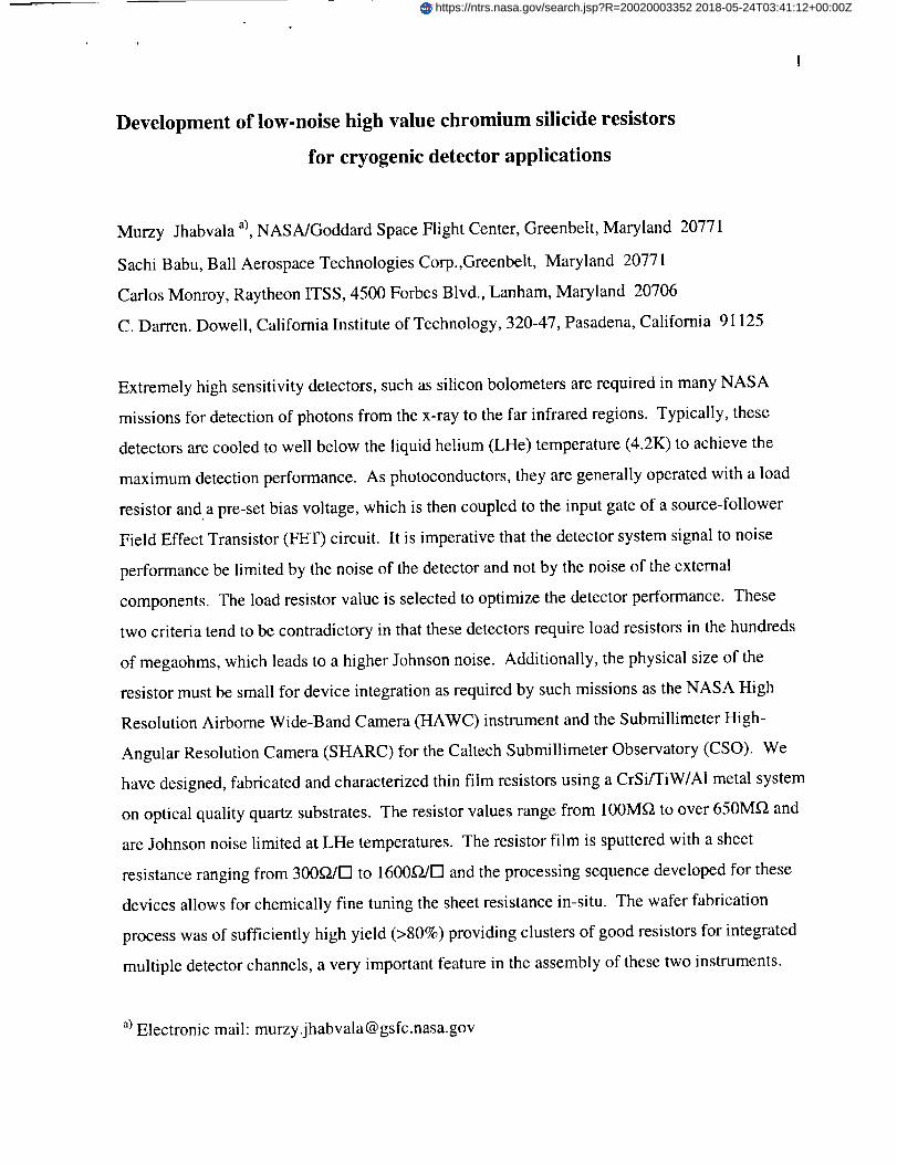
applied and the signal is extracted, as shown in figure 1 below. This method has been used in the
Infrared Astronomical Satellite (IRAS), NASA's Cosmic Background Explorer (COBE),
numerous DoD missions, many ground-based astronomy telescopes and is
VB
I VDD
--
Detector Rs(0.2 K) 300 K)
_1_w
FIG 1. Source-follower JFET circuit employed in low noise, high performance detector
systems.
currently the method to be employed by the future High Resolution Airborne Wide-Band
Camera (HAWC) to be installed on the SOFIA (Stratospheric Observatory for Infrared
Astronomy) Boeing 747 aircraft astronomy platform and by the ground based Submillimeter
High-Angular Resolution Camera (SHARC) to be installed on the Caltech (California Institute of
Technology) Submillimeter Observatory (CSO). ASTRO-E is a future NASA mission, which
hassimilar loadresistor-preamprequirements.HAWC will bea facility instrumentproviding
userswith thebestangularresolutionin the40-300micrometerIR spectralregion. It is intended
to providedataonawide rangeof astronomicalphenomenon,sucha,starformationin our own
andin distantgalaxies2. TheHAWC instrumentdevelopmentis ahighlycollaborativeeffort
betweentheUniversityof Chicago,California Instituteof TechnologyandNASA's Goddard
SpaceFlight Center(GSFC). TheSHARCinstrumentis acollaborativeeffort betweenCaltech
andGSFCalsointendedto searchfor andprovidedataaboutextragalacticsource
emissions3. Both instrumentsarebasedon therecentlydeveloped"pop-up"bolometerMEMS
technologydevelopedbyH. MoselelyandC. Allen of theGoddardSpaceFlight Center1. The
circuit in Figure 1is simplein principlebutextractingthemaximumperformancefrom the
detectorcanbequitechallenging.Duringoperation,incidentradiationis absorbedby the
detector,whichrespondsby undergoingachange(decrease)in impedance.Theinstantaneous
detectorvoltage,VD,is simply:
andtheoutputvoltageVo,is
Vo = G VD,
whereG is thegainof thesource-followerandgenerallyrangesfrom 0.8-0.98. To obtainthe
maximumsensitivity,thedetectorsignal-to-noiseratiomustbelimited by thedetectornoiseand
notby thenoisefrom othersystemcomponents.The mostegregiousnoiseoffenderstendto be
theloadresistorsandtheJFETandto minimizethis effectextraordinarydesignsare
implemented.TheJFETsarecarefullyevaluatedto locatetheiroptimumoperatingtemperature.
Theresistorsaredesignedsothattheirvalue(typically 10-20timesthedetectordark resistance)
optimizesthedetectorresponsivityandmustbefabricatedto beJohnsonnoiselimited. For the
HAWC anSHARCinstrumentsthis translatesto individually screenedJFETsoperatingat 110K,
resistorsof 350-450M_ for HAWC and100-200Mg2for SHARCoperatingnear4.2K. Both
instrumentsarebaseliningafocalplanearrayof 12x 32 (384)detectorelements,eachdetector
requiringaloadresistorandJFET. Thispaperwill describethedevelopmentof the load
4
resistorsfor theseprojectsatNASA's GoddardSpaceFlight Center.We will describethe
design,fabrication,assemblyandpresenttestresultsof resistorswe fabricated.
II. DESIGN AND FABRICATION
A custom resistor pattern was developed to bracket the desired resistance values of 100-200MfZ
for SHARC and 350-450M_ for HAWC. However, the critical performance metric is the noise
of the device at its operating temperature and should be Johnson noise limited. Experiments
were conducted to determine the minimum CrSi film thickness we were confident would not
introduce excess noise as the resistors were processed (dicing, for example), assembled and
cryogenically cycled. This film thickness would then drive the resistor design. The minimum
CrSi thickness we implemented was nominally around 570]k yielding a resistivity of 1.06-
1.16KD_,/r-I. Another constraint was the yield consideration. Each instrument requires 384
individual load resistors, which is further complicated by the various operating temperatures
required of the three components (detector, load resistor and JFET). The detectors are located at
the focal plane and operate at T<0.06K. The JFETs will be operated at 110K and the load
resistors will operate near the liquid helium bath temperature of 4.2K. The three components are
electrically connected but must be kept thermally isolated yet remains in close proximity to each
other. To accomplish this, the load resistors and JFETs are mounted on their own ceramic carrier
boards and then interconnected using the Goddard developed silicon bridge chip technology 4.
Each instrument contains 384 detectors electrically divided into three groups of 128 channels.
The 384 JFETs are individually "hand" mounted onto a ceramic board and then cryogenically
rescreened and replaced, if necessary. The resistors can be mounted in groups of up to 32
(depending on the contiguous yield) so conceivably one board can be populated with just four
resistor segments as opposed to 128 individual die. Therefore one of the resistor design
considerations is selecting an appropriate geometry which achieves the desired resistance value
in the allotted real estate but keeps the line width large enough to maximize the yield. These two
constraints lead to a serpentine structure in a rectangular area of 25 mils by 1100 mils. The lines
and spaces are drawn at 4.0 microns and each resistor has 3,425 segments for a total of
approximately 425,0001-'1s. The 25-mil width was an instrument constraint to meet a 25-mil
channel-to-channel pitch. Each resistor was designed to have a single bond pad at one end and
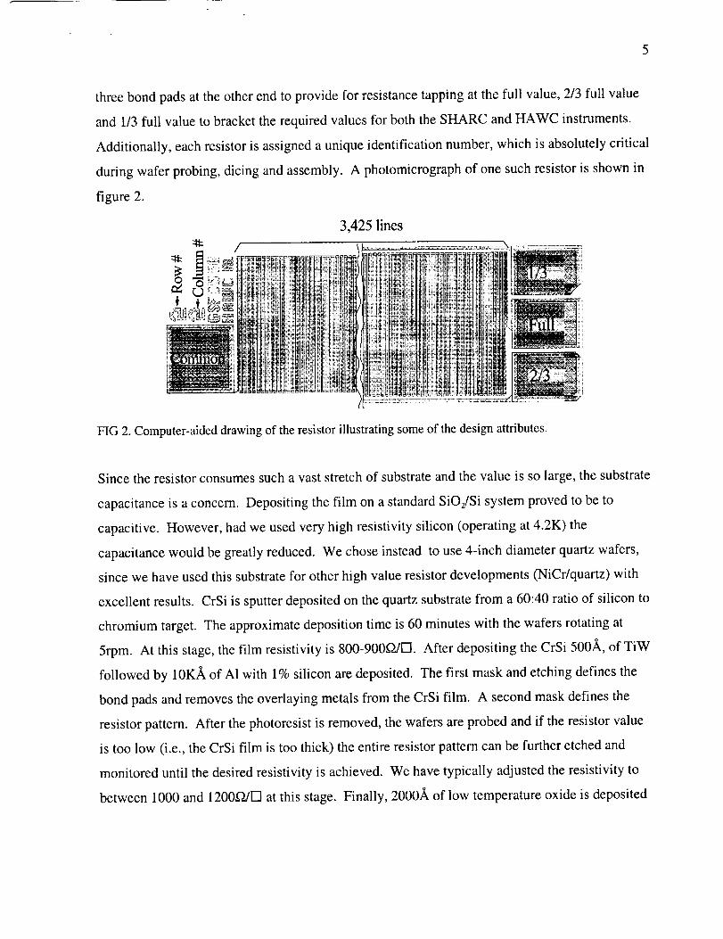
threebondpadsattheotherendto providefor resistancetappingatthefull value,213full value
and1/3full valueto brackettherequiredvaluesfor both theSHARCandHAWC instruments.
Additionally, eachresistoris assignedauniqueidentificationnumber,which is absolutelycritical
duringwaferprobing,dicingandassembly.A photomicrographof onesuchresistoris shownin
figure 2.
3,425lines
FIG2.Computer-aideddrawingoftheresistorillustratingsomeof thedesignattributes.
Sincetheresistorconsumessucha vaststretchof substrateandthevalueis so large,thesubstrate
capacitanceis aconcern.Depositingthefilm onastandardSiO2/Sisystemprovedto beto
capacitive.However,hadweusedveryhigh resistivitysilicon (operatingat4.2K) the
capacitancewouldbegreatlyreduced.We choseinsteadto use4-inchdiameterquartzwafers,
sincewehaveusedthis substratefor otherhigh valueresistordevelopments(NiCr/quartz)with
excellentresults.CrSi is sputterdepositedon thequartzsubstratefrom a 60:40ratioof silicon to
chromiumtarget. Theapproximatedepositiontimeis 60minuteswith thewafersrotatingat
5rpm. At this stage,thefilm resistivity is 800-900DJD.After depositingtheCrSi 500_, of TiW
followedby 10K/_,of A1with 1%siliconaredeposited.Thefirst maskandetchingdefinesthe
bondpadsandremovestheoverlayingmetalsfromtheCrSi film. A secondmaskdefinesthe
resistorpattern. After thephotoresistis removed,thewafersareprobedandif theresistorvalue
is too low (i.e.,theCrSi film is toothick) theentireresistorpatterncanbe furtheretchedand
monitoreduntil thedesiredresistivity is achieved.Wehavetypically adjustedtheresistivityto
between1000and 1200D,/Datthis stage.Finally, 2000_of low temperatureoxideis deposited
andthebondpadareasopened.
HF in aratioof 60:5:1.
Theetchantfor theCrSi film is amixture5of H3PO4,HNO3and
IlL RESULTS
Since these devices are to be integrated into a flight detector assembly, there are additional
screening criteria other than just functional performance. The additional criteria include:
1. Johnson noise limit performance at cryogenic temperatures
2. Voltage and temperature coefficients (R vs. V and R vs. T)
3. Contiguous device yield
4. Device to device matching
5. Cryogenic cycling
A. Temperature, voltage and noise performance
The test resistors were mounted in a large 1.5"x.75" Kovar header. Although directly
mounted on the LHe cold surface, there was a substantial thermal rise to the resistors and
temperature sensor, which was mounted, on the topside of the package. The dewar used for these
tests is multipurpose and the wiring harness posed a substantial thermal load The lowest
temperature we were able to achieve during the actual noise measurements was 10K. Our noise
measurement system is in an isolated screen room, which prevents LHe transfer. However, the
DC resistance measurements were taken in proximity to our helium source and therefore we
were able to refresh the reservoir as necessary. These DC measurements were made at 5K.
After assessing functionality at room temperature, 77K and 5K, the noise performance of the
resistors was evaluated. In the past, we have encountered excess noise (from otherwise good
resistors) as a result of wafer processing methods. Some problems have been the noise generated
when an interface oxide layer is inadvertently introduced between the metal films and a second
problem has been the introduction of microcracks in the resistor film from wafer dicing, thermal
stresses and improper handling. Drawing on our past experience with thin film NiCr resistors we
had previously fabricated, we encountered no excess noise in these CrSi resistors at the test
temperatures of 300K, 77K and 10K. We also did not see additional noise as a function of
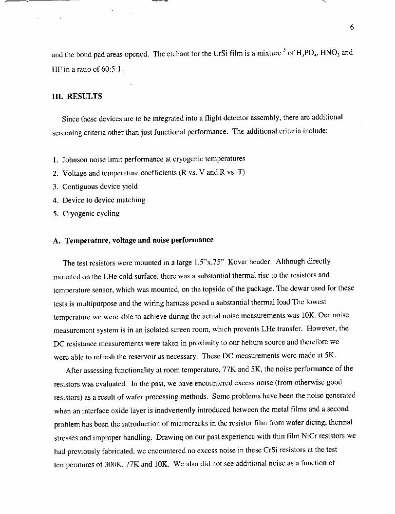
resistorbiasvoltage. We did observeavoltageandtemperaturecoefficient(at5K) which will be
described.TheresistorsandJFETsweremountedinsidealiquid heliumcryostat.A seriesof DC
electricaltestswerefirst performed.Measurementsof theJFETgain(>.95),resistanceand
resistancevs.biasweremadeat roomtemperature(T=295K),77K and5K. Theplotsof figure 3
showtheresistanceasafunctionof temperatureandbias. Threeresistors(arbitrarilyR1, R2and
R3),eachnominally280M_ at 295Kweremeasured.TheresistorsR1andR2weremeasured
asacombinedseriespairandR3wasmeasuredasasingle280M_ resistor.Themeasurement
serieswith ananoammeterto measuretheresistorcurrent.methodusedavoltagesourcein(;50 .... .......
8OO
560
v ._[10
380
3OO
250
650
600
550
500
450
4O0
350
3O0
2500
............ -- ----dT_
1 2 3 4 5 iS 7 $
Bias (V)
FIG 3. Resistance as a function of voltage at T=295K, 77K and 10K for a single
280 Mr2 resistor and two resistors in series totaling 560 Mr2.
The thermal coefficient of resistance (TCR) for these devices is calculated from
a=--R0
For R0 equal to the room temperature resistance, c_ ranges from -1 x 10-_/K to -4x 10-_/K.
However, the resistance was highest at 77K and therefore the TCR from 77K to 5K is positive
(=4x 10_FK).
The voltage coefficient, VCR, at a specific temperature is similarly defined as
a = _ _ = R(V_)(Vz - V_)
The accuracy of the ammeter at very low bias voltage levels made it difficult to obtain a near
zero bias resistance. However, over the 1-7 voltage range the VCR was typically =5x10³/V.
Over the range of the detector operation where the current through the resistor is almost constant
8
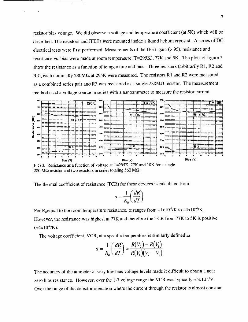
thisrepresentsan insignificantvariation. Uponcompletionof theseDC tests,noisespectrawere
obtained.TheJohnsonnoisevoltage,V,, is given by
V. = /4kTBR
where,
k=Boltzmann' s constant, 1.38x 10 .23W-sec/K
T =temperature (K)
B = measurement bandwidth
R = resistor value
The frequency spectrum of concern is that below 200 Hz and of particular concern is the low
frequency performance below 30 Hz. In the first test one end of the 280M_ was grounded
inside the dewar and the noise was measured with the JFET source-follower connected to an
Ithaco 1201 amplifier (gain set to 20) and an HP 35670A signal analyzer. Figure 4 shows the
noise spectrum at three temperatures normalized to unity bandwidth and gain.
IE
l"5Z
2
1.5 --
1
0.5 .......
0
i ii- ZI 2]EZ
iii ij K! ....... "twt',_.i
..... li p,_a-;-.-:rr.._-........
i
_ mbmt_
50 100
Frequency (Hz)
150 200
FIG 4. The test configuration and noise spectra for a single 280 Mff2 CrSi resistor at T=295K,
77K and 10K.
The calculated values are listed below for the single 280Mff2 resistor.
ILK) ¥n(_tV/Hz uz}
295 2.13
77 1.09
10 0.4
Thesevaluesarein excellentagreementwith the acquireddataat frequenciesbelow=20Hz.The
noisevoltageattenuationasafunctionof frequencyis aresultof theshuntingcapacitanceacross
the280Mff2resistor.TheconditionwhereRC= l/2rff occursatthefrequencywherethevoltage
is reducedto .707of theDC or low frequencyvalue.From thenoisespectrathis frequencyis
between60-80Hzcorrespondingto acapacitiveloadof 5.6pF-7.5pF.This is essentiallythe
parasiticcapacitanceof theresistor-JFETcombination.
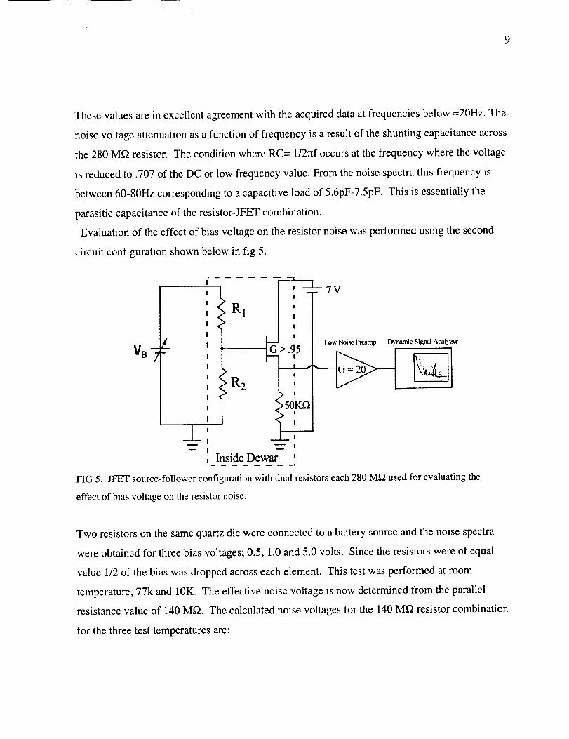
Evaluationof theeffectof biasvoltageon theresistornoisewasperformedusingthesecond
circuit configurationshownbelowin fig 5.
iI, l iT, --,- 7V, RII
I I
I
_2_'I
, Inside Dewar '_J
FIG 5. JFET source-follower configuration with dual resistors each 280 Mg2 used for evaluating the
effect of bias voltage on the resistor noise.
Two resistors on the same quartz die were connected to a battery source and the noise spectra
were obtained for three bias voltages; 0.5, 1.0 and 5.0 volts. Since the resistors were of equal
value 1/2 of the bias was dropped across each element. This test was performed at room
temperature, 77k and 10K. The effective noise voltage is now determined from the parallel
resistance value of 140 M_. The calculated noise voltages for the 140 M_ resistor combination
for the three test temperatures are:
10
V.(._V/Hz m)
295 1.5
77 0.77
10 0.28
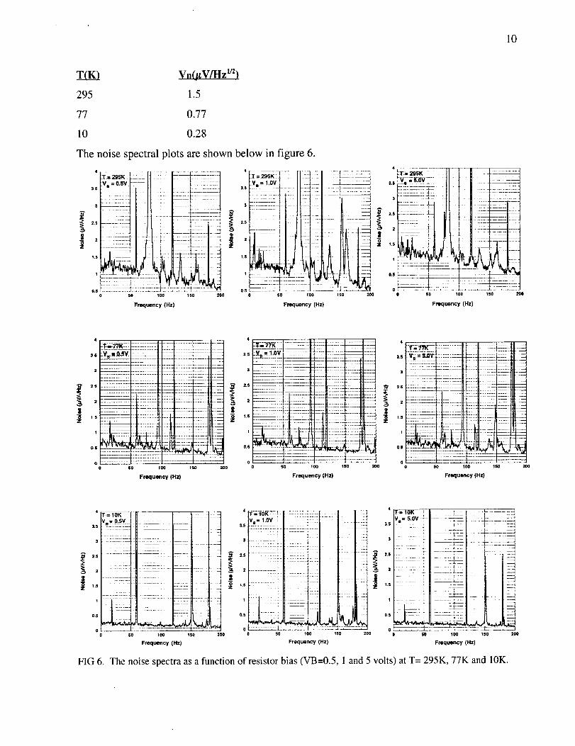
The noise spectral plots are shown below in figure 6.
|
4
T _ 2951< :_::
V_ = 0,SV _-_-3.5
.... --:: ::I3 ...... -,
- 2 212___Z2._ i
,.,2:5:5-:71
2 • 4
1.5
1
-22 --2_ ---_--2--_.2o,6 .....................
o so
+- I +
L
,ti1
too
+i_5'_5. ........
......+ .......
-{....... _-::::+
....._i.i_i-ii !_
I1 I: 5
150 200
Frequency (Ha)
4
3.5
3
2,5
_ 2I
I.S
1
0.S
--
50 t00 150 200
Frequency (Ha)
,t__ _ __i_-_-_÷_i_0 S0 100 150 200
Frequency (Hz)
.,@
4 I
+_-]i:i ....
....... ÷......
..... + .......... + ......
2.5 _ ......
1,5 ----_ .....
........ + .....
o 5o
_A--- I- .......... 4--
:_:_22.: .......
.... _!11=-- H-_--- t -
_+ ii --
+_ _-_÷__÷......
Ioo 15o 2OO
Frequency (Hz)
A
4
.... + -- j...............
'-- __., ___Z .................
+ iiii- ii+-..'2 '-----'-"-_---_
:_----_-::::I :::-: _
........... + _-- I_.s "-_ _ :_:: "_ 1.s
.l--i
0.5 _ ...... O.S
°_1 oo so lOO 15o 2oo
Frequency (Hz)
Y;; --_ ::
........ + +
so
......IF......._............ L.
......._ ....... :_ ..............+L ..... S__
- -i+ ....... ,-
_2-_E_L:]i?_-?_-_--=
100 150 200
Fr_lu_'_cy (Hz)
4 _
,I::!iiii!il:.: I
I_._._,+ i:'I:
O.S
0 5O
m_
-::. -_
_2:!-i-!_
"i I---+I i ; ' +
100 150 200
Frequency (Hz)
4 _:_i)__-::!I
3.5 ......... +
+ .. _ +
.......... ÷_!
.__ +_+2.5 + ,
I.sI
I '0,5
o_o so
-- __::i] ::i
, ::T22lOO 15o
Frequency (Hz)
2OO
4
--"Z .... _LJt.. __ ! --
:.::+.__ ........._
] -_.... i --_1 -- 1 _ --t-- i
0.5 _ --_
o 50 loa 15o 200
Frequency (Hz)
FIG 6. The noise spectra as a function of resistor bias (VB=0.5, 1 and 5 volts) at T= 295K, 77K and 10K.
11
Of particularnoteis the invarianceof thespectraamplitudewith increasingbiasvoltagefrom 0
to 5.0volts (2.5volts acrosseachresistor).Theacquireddatais in excellentagreementwith the
calculateddataatlow frequencies.Most of the largespikesarethe60Hz andharmonicswhich
areomnipresentin terrestrialtestconfigurations.Thereareotherspuriousnoisespikesthatresult
from thedewarmicrophonicsandexternalelectricalequipmentemissions.
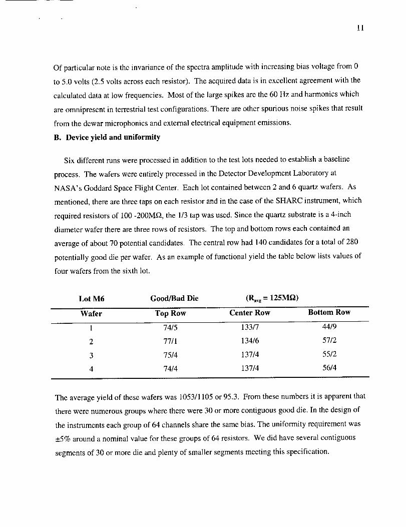
B. Device yield and uniformity
Six different runs were processed in addition to the test lots needed to establish a baseline
process. The wafers were entirely processed in the Detector Development Laboratory at
NASA's Goddard Space Flight Center. Each lot contained between 2 and 6 quartz wafers. As
mentioned, there are three taps on each resistor and in the case of the SHARC instrument, which
required resistors of 100 -200MK2, the 1/3 tap was used. Since the quartz substrate is a 4-inch
diameter wafer there are three rows of resistors. The top and bottom rows each contained an
average of about 70 potential candidates. The central row had 140 candidates for a total of 280
potentially good die per wafer. As an example of functional yield the table below lists values of
four wafers from the sixth lot.
Lot M6 Good/Bad Die (R_v_ = 125M_)
Wafer Top Row Center Row Bottom Row
1 74/5 133/7 44/9
2 77/1 134/6 57/2
3 75/4 137/4 55/2
4 74/4 137/4 56/4
The average yield of these wafers was 1053/1105 or 95.3. From these numbers it is apparent that
there were numerous groups where there were 30 or more contiguous good die. In the design of
the instruments each group of 64 channels share the same bias. The uniformity requirement was
_+5% around a nominal value for these groups of 64 resistors. We did have several contiguous
segments of 30 or more die and plenty of smaller segments meeting this specification.
12
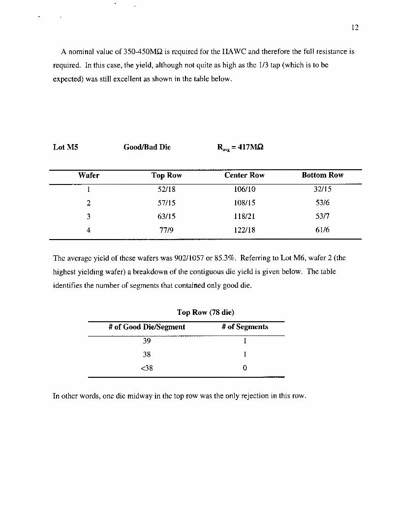
A nominalvalueof 350-450Mg2is requiredfor theHAWC andthereforethefull resistanceis
required. In thiscase,theyield, althoughnotquite ashigh asthe1/3tap(which is to be
expected)wasstill excellentasshownin thetablebelow.
Lot M5 Good/Bad Die R_vg = 417M_
Wafer Top Row Center Row Bottom Row
1 52/18 106/10 32/15
2 57/15 108/15 53/6
3 63/15 118/21 53/7
4 77/9 122/18 61/6
The average yield of these wafers was 902/1057 or 85.3%. Referring to Lot M6, wafer 2 (the
highest yielding wafer) a breakdown of the contiguous die yield is given below. The table
identifies the number of segments that contained only good die.
Top Row (78 die)
# of Good Die/Segment # of Segments
39 1
38 1
<38 0
In other words, one die midway in the top row was the only rejection in this row.
13
Middle Row (140 die)
# of Good Die/Segment # of Segments
60 1
26 1
10- 12 4
<10 0
Bottom Row (59 die)
# of Good Die/Segment # of Segments
28 2
On this wafer the resistance values ranged from 109M_ to 166 M_. In a given row, however,
the variation amongst any contiguous 12 die was a maximum of 6% between the high and low
value and in some cases less than 0.5%.
C. Cryogenic cycling
During the course of an instrument build, many components of a cryogenic system will be
subjected to numerous cooling cycles throughout its mission lifetime. In some cases, many
dozens of thermal cycles may be encountered, in more extreme cases only a few cycles may be
permitted. In any case, the devices will experience some number of thermal cycles and it is
expected and generally required that not only will the devices survive mechanically but that their
stability also remain unchanged or at the very least highly predictable. To this end two quartz
strips containing nine resistors were epoxy mounted to a HAWC load resistor ceramic board.
After a 100C epoxy cure and cool the resistors were directly immersed into LN2, thermally
equilibrated to 77K and then removed. The resistors were then rapidly brought to room
temperature with the help of a heat gun. This process was repeated for a total of 10 LN2 soaks.
Generally, the cooldown from room temperature to 77K wilt manifest any failures due to thermal
14
shocks.If adevicesurvivesthis testwehavehighconfidencethatthedevicewill remain
mechanicallystablethroughoutcryogeniccycling. Theresistanceof all ninedeviceswas
measuredinitially in June,2000,thenagainimmediatelybeforethefirst LN2 immersionon
October26,2000andagainafterthetenthimmersionin LN2 alsoonOctober26,2000. All nine
resistorswerewithin .5%of their initial value,thevariability of themeasurementsystem.In
Marchof 2001weagainmeasuredthevalueof eachresistorandthenimmersedthesampleinto
LHe, allowedtimefor equilibrationthenremovedandbroughtthedeviceto roomtemperature
(with theaidof theheatgun). We repeatedthissequencefor five LHe soaksandthen
remeasuredtheresistors.To within ourmeasuringaccuracyeachof thenineresistorswas
exactlythevaluewehadmeasuredin June,2000.
III. SUMMARY
The need for high value, integrated resistors capable of operating at liquid helium temperatures
has been a nagging issue for decades in the astronomy and low temperature physics
communities. Although resistors are technologically one of the least complex electronic
components their evolution has not kept pace with advanced detector technology. We have
presented results indicating we have breached the gap between resistor technology and detector
technology. The CrSi resistors we have fabricated can easily exceed 250 Mg2, operate at low
temperatures, can be integrated on silicon, quartz or sapphire substrates and can be manufactured
with high yield using relatively standard IC photolithograhic processes.
As part of our future efforts to improve detector performance we will be integrating these
resistors directly with silicon microbolometer arrays not only improving system performance by
Locating the resistors in close proximity to the detector but by also reducing the wire
interconnects that are sources of microphonic noise generation. The overall resistor production
is relatively inexpensive and the manufacturing time relatively short.
Acknowledgement
The authors would like to express their appreciation to Harvey Moseley, Dave Franz, Frank
Peters, Carol Sappington, Peter Shu, Wayne Smith, George Voellmer and Arlin Bartels...
15
i S.H. Moseley,Jr.,C.D.DoweIl,C. A Allen andT.G Phillips,ASPConferenceSeries217,140,
editedby J.G. MangumandS.J.E.Radford(2000).
2A. Harperet al, Proceedingsof SPIE,4014,43 (2000).
3D. Dowell, S.H. MoseleyandT. Phillips,ASPConferenceSeries217,105,editedby J.G.
MangumandS.J.E.Radford(2000).
4C.Allen, S.H. Moseley,D. S.SchwingerandD.E.Franz,presentedatNanospace1998,
Houston,Texas.
5L. MaisselandR. Glang,Handbook of Thin Film Technology (McGraw-Hill 1970).