gate stack and silicide issues in silicon processing...
TRANSCRIPT
Gate Stack and SilicideIssues in Silicon Processing II
www.cambridge.org© in this web service Cambridge University Press
Cambridge University Press978-1-107-41219-4 - Materials Research Society Symposium Proceedings: Volume 670:Gate Stack and Silicide Issues in Silicon Processing IIEditors: S. A. Campbell, L. A. Clevenger, P. B. Griffin and C. C. HobbsFrontmatterMore information
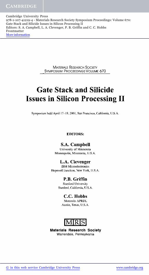
MATERIALS RESEARCH SOCIETYSYMPOSIUM PROCEEDINGS VOLUME 670
Gate Stack and SilicideIssues in Silicon Processing II
Symposium held April 17-19,2001, San Francisco, California, U.S.A.
EDITORS:
S.A. CampbellUniversity of Minnesota
Minneapolis, Minnesota, U.S.A.
L.A. ClevengerIBM Microelectronics
Hopewell Junction, New York, U.S.A.
P.B. GriffinStanford University
Stanford, California, U.S.A.
C.C. HobbsMotorola APRDL
Austin, Texas, U.S.A.
Materials Research SocietyWarrendale, Pennsylvania
www.cambridge.org© in this web service Cambridge University Press
Cambridge University Press978-1-107-41219-4 - Materials Research Society Symposium Proceedings: Volume 670:Gate Stack and Silicide Issues in Silicon Processing IIEditors: S. A. Campbell, L. A. Clevenger, P. B. Griffin and C. C. HobbsFrontmatterMore information
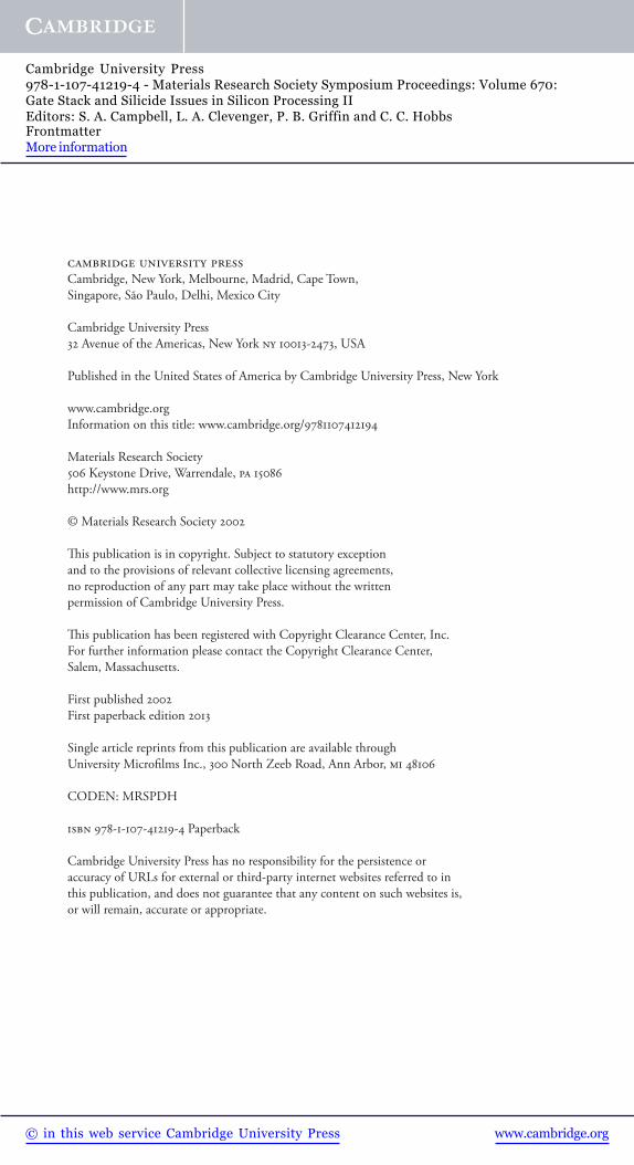
cambridge university press Cambridge, New York, Melbourne, Madrid, Cape Town, Singapore, São Paulo, Delhi, Mexico City
Cambridge University Press32 Avenue of the Americas, New York ny 10013-2473, USA
Published in the United States of America by Cambridge University Press, New York
www.cambridge.orgInformation on this title: www.cambridge.org/9781107412194
Materials Research Society506 Keystone Drive, Warrendale, pa 15086http://www.mrs.org
© Materials Research Society 2002
This publication is in copyright. Subject to statutory exceptionand to the provisions of relevant collective licensing agreements, no reproduction of any part may take place without the written permission of Cambridge University Press.
This publication has been registered with Copyright Clearance Center, Inc.For further information please contact the Copyright Clearance Center,Salem, Massachusetts.
First published 2002 First paperback edition 2013
Single article reprints from this publication are available throughUniversity Microfilms Inc., 300 North Zeeb Road, Ann Arbor, mi 48106
CODEN: MRSPDH
isbn 978-1-107-41219-4 Paperback
Cambridge University Press has no responsibility for the persistence oraccuracy of URLs for external or third-party internet websites referred to inthis publication, and does not guarantee that any content on such websites is,or will remain, accurate or appropriate.
www.cambridge.org© in this web service Cambridge University Press
Cambridge University Press978-1-107-41219-4 - Materials Research Society Symposium Proceedings: Volume 670:Gate Stack and Silicide Issues in Silicon Processing IIEditors: S. A. Campbell, L. A. Clevenger, P. B. Griffin and C. C. HobbsFrontmatterMore information
CONTENTS
Preface xi
Materials Research Society Symposium Proceedings xii
HIGH-k MA TERIALS
* Materials and Physical Properties of Novel High-k and Medium-kGate Dielectrics Kl.l
Ran Liu, Stefan Zollner, Peter Fejes, Rich Gregory, Shifeng Lu,Kim Reid, David Gilmer, Bich-Yen Nguyen, Zhiyi Yu,Ravi Droopad, Jay Curless, Alex Demkov, Jeff Finder,and Kurt Eisenbeiser
Ultra-Thin Zirconium Oxide Films Deposited by Rapid ThermalChemical Vapor Deposition (RT-CVD) as Alternative GateDielectric K1.4
Jane P. Chang and You-Sheng Lin
PROCESSING OF HIGH-kGA TE DIELECTRICS
* Challenges in Integrating the High-k Gate Dielectric Film to theConventional CMOS Process Flow K2.1
Avinash Agarwal, Michael Freiler, Pat Lysaght,Loyd Perrymore, Renate Bergmann, Chris Sparks, Bill Bowers,Joel Barnett, Deborah Riley, Yudong Kim, Billy Nguyen,Gennadi Bersuker, Eric Shero, Jae E. Lim, Steven Lin,Jerry Chen, Robert W. Murto, and Howard R. Huff
Engineered Tantalum Aluminate and Hafnium Aluminate ALDFilms for Ultrathin Dielectric Films With Improved Electrical andThermal Properties K2.2
Robert B. Clark-Phelps, Anuranjan Srivastava, Lance Cleveland,Thomas E. Seidel, and Ofer Sneh
High Permittivity Oxide Gate Stacks on Silicon IncorporatingUHV Silicon Nitride Interfacial Layers K2.3
Mark A. Shriver, Ann M. Gabrys, T.K. Higman,and S.A. Campbell
Alternating Layer Chemical Vapor Deposition (ALD) of MetalSilicates and Oxides for Gate Insulators K2.4
Roy G. Gordon, Jill Becker, Dennis Hausmann, and Seigi Suh
* Invited Paper
www.cambridge.org© in this web service Cambridge University Press
Cambridge University Press978-1-107-41219-4 - Materials Research Society Symposium Proceedings: Volume 670:Gate Stack and Silicide Issues in Silicon Processing IIEditors: S. A. Campbell, L. A. Clevenger, P. B. Griffin and C. C. HobbsFrontmatterMore information
Characterization of TiO2 Films Grown at Low Temperatures forAlternative Gate Dielectric Application K2.10
Jun-Ying Zhang and Ian W. Boyd
GATE STACK AND SUICIDE ISSUESIN Si PROCESSING II
Promising Gate Stacks With Ru and RuO2 Gate Electrodes andY-Silicate Dielectrics K3.1
Huicai Zhong, Greg Heuss, You-Seok Suh, Shin-Nam Hong,Veena Misra, Jason Kelly, and Gregory Parsons
Preliminary First Principles Study of Hf and Zr Aluminates asReplacement High-k Dielectrics K3.2
Michael Haverty, Atsushi Kawamoto, Gyuchang Jun,Kyeongjae Cho, and Robert Dutton
Development of Polycide Application and Control of ProcessConditions on DCS Based WSix K3.6
Young-Kyou Park, Jaihyung Won, Ju-Hwan Park,and Jung-Ho Park
Effect of Pre-Cooling Treatment on the Formation of C54 PhaseTitanium Silicide K3.7
Lin Zhang and Yong Keun Lee
ELECTRICAL PERFORMANCE OFNOVEL GATE DIELECTRICS
* Chemical Vapor Deposition of Titania/Silica and Zirconia Films K4.1Wayne L. Gladfelter, Ryan C. Smith, David Burleson,Charles J. Taylor, Jeffrey T. Roberts, Stephen A. Campbell,Noel Hoilien, Mike Tiner, Rama Hegde, and Christopher Hobbs
Transistors Built With ZrO2 and HfO2 Deposited From Nitratos K4.2Stephen A. Campbell, Noel Hoilien, Tiezhong Ma, Fang Chen,Ryan Smith, and Wayne Gladfelter
Electrical Characteristics of TaOxNy/ZrSixOy Stack GateDielectric for MOS Device Applications K4.6
Hyungsuk Jung, Hyundoek Yang, Kiju Im, and Hyunsang Hwang
* Invited Paper
VI
www.cambridge.org© in this web service Cambridge University Press
Cambridge University Press978-1-107-41219-4 - Materials Research Society Symposium Proceedings: Volume 670:Gate Stack and Silicide Issues in Silicon Processing IIEditors: S. A. Campbell, L. A. Clevenger, P. B. Griffin and C. C. HobbsFrontmatterMore information
Electrical and Structural Characteristics of Ultra-ThinTiO2/Ti-Si-O Stacked Gate Insulator Formed by RF SputteringTechnique K4.7
M. Koyama, A. Kaneko, M. Koike, I. Fujiwara, M. Yabuki,M. Yoshiki, M. Koike, and A. Nishiyama
Investigation on the Thermal and Electrical Properties of Ti-Si-OFilm Formed by the Composite Sputtering Deposition K4.8
Akira Nishiyama, Akio Kaneko, Masato Koyama,Yoshiki Kamata, Ikuo Fujiwara, Masahiro Koike,Masahiko Yoshiki, and Mitsuo Koike
Comparison of Conductance and Capacitance Techniques forMeasurement of Interface States in Thin Oxides K4.9
T.K. Higman
NOVEL GATE STRUCTURES
Dual Work Function CMOS Gate Technology Based on MetalInterdiffusion K5.1
Igor Polishchuk, Pushkar Ranade, Tsu-Jae King,and Chenming Hu
Molybdenum Gate Electrode Technology for Deep Sub-MicronCMOS Generations K5.2
Pushkar Ranade, Ronald Lin, Qiang Lu, Yee-Chia Yeo,Hideki Takeuchi, Tsu-Jae King, and Chenming Hu
Reduction of Whisker-Originated Short Between W Polymetaland Contact Plug K5.6
Yasushi Akasaka, Hiroshi Suzuki, Yuji Yokoyama,Nobuaki Yasutake, Hitomi Yasutake, Susumu Yoshikawa,Yusuke Kohyama, Yoshio Ozawa, Katsuhiko Hieda,Kyoichi Suguro, and Toshihiro Nakanishi
Annealing Behavior of WSix Films Prepared by CVD K5.7M. Katiyar, G.S. Samal, R.K. Gupta, Deepak, P.K. Sahoo,V.N. Kulkarni, and O. Adetutu
The Electrical Characteristics of the MOSCAP Structures WithW/WNx/poly SilxGexGates Stack K5.9
S.-K. Kang, JJ. Kim, D.-H. Ko, T.H. Ahn, I.S. Yeo, T.W. Lee,and Y.H. Lee
A Study on the Polycrystalline Silicon Germanium Gate ElectrodeFabrication Technology for Cobalt Silicide Process K5.10
Hidekazu Sato, Takae Sukegawa, Toshifumi Mori,Kousuke Suzuki, and Haruhisa Mori
vii
www.cambridge.org© in this web service Cambridge University Press
Cambridge University Press978-1-107-41219-4 - Materials Research Society Symposium Proceedings: Volume 670:Gate Stack and Silicide Issues in Silicon Processing IIEditors: S. A. Campbell, L. A. Clevenger, P. B. Griffin and C. C. HobbsFrontmatterMore information
NOVEL SUICIDE PROCESSES
X-ray Techniques for Silicides K6.2Douglas J. Tweet, Jer-shen Maa, and Sheng Teng Hsu
Effects of a Ta Interlayer on the Titanium Silicide Reaction: C40Formation and Higher Scalability of the TiSi2 Process K6.3
F. La Via, S. Privitera, F. Mammoliti, and M.G. Grimaldi
Direct Formation of C54 Phase on the Basis of C40 TiSi2 and ItsApplications in Deep Sub-Micron Technology K6.4
S.Y. Chen, Z.X. Shen, S.Y. Xu, A.K. See, L.H. Chan,and W.S. Li
Increased Thermal Stability of Co-Silicide Using Co-Ta AlloyFilms K6.5
Min-Joo Kim, Hyo-Jick Choi, Dae-Hong Ko, Ja-Hum Ku,Siyoung Choi, Kazuyuki Fujihara, Ho-Kyu Kang,and Hoo-Jeung Lee
A Comparative Study of Nickel Silicide Formation Using aTitanium Cap Layer and a Titanium Interlayer K6.6
W.L. Tan, K.L. Pey, Simon Y.M. Chooi, and J.H. Ye
The Influence of Ti and TiN on the Thermal Stability of CoSi2 K6.7C. Detavernier, Guo-Ping Ru, R.L. Van Meirhaeghe,and K. Maex
Stability Improvement of Nickel Silicide With Co Interlayer on Si,Polysilicon and SiGe K6.9
Jer-shen Maa, Douglas J. Tweet, Yoshi Ono, Lisa Stecker,and Sheng Teng Hsu
Silicide Formation for Ni and Pd Bilayers on Si(100) Substrates K6.10Xin-Ping Qu, C. Detavernier, R.L. Van Meirhaeghe,and F. Cardon
SHALLOW JUNCTIONS ANDINTEGRATION ISSUES INFEOL
Electrical Performance and Scalability of Ni-MonosilicideTowards sub 0.13 um Technologies K7.1
Anne Lauwers, Muriel de Potter, Richard Lindsay, An Steegen,Nico Roelandts, Fred Loosen, Christa Vrancken, and Karen Maex
Vlll
www.cambridge.org© in this web service Cambridge University Press
Cambridge University Press978-1-107-41219-4 - Materials Research Society Symposium Proceedings: Volume 670:Gate Stack and Silicide Issues in Silicon Processing IIEditors: S. A. Campbell, L. A. Clevenger, P. B. Griffin and C. C. HobbsFrontmatterMore information
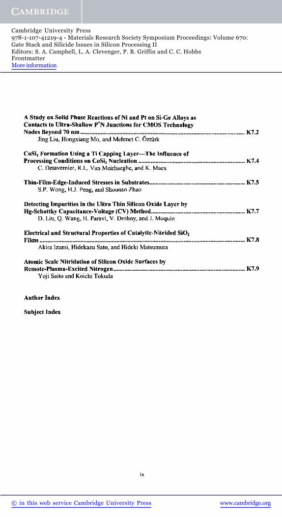
A Study on Solid Phase Reactions of Ni and Pt on Si-Ge Alloys asContacts to Ultra-Shallow P+N Junctions for CMOS TechnologyNodes Beyond 70 nm K7.2
Jing Liu, Hongxiang Mo, and Mehmet C. Ozturk
CoSi2 Formation Using a Ti Capping Layer—The Influence ofProcessing Conditions on CoSi2 Nucleation K7.4
C. Detavernier, R.L. Van Meirhaeghe, and K. Maex
Thin-Film-Edge-Induced Stresses in Substrates K7.5S.P. Wong, H.J. Peng, and Shounan Zhao
Detecting Impurities in the Ultra Thin Silicon Oxide Layer byHg-Schottky Capacitance-Voltage (CV) Method K7.7
D. Liu, Q. Wang, H. Paravi, V. Drobny, and J. Moquin
Electrical and Structural Properties of Catalytic-Nitrided SiO2
Films K7.8Akira Izumi, Hidekazu Sato, and Hideki Matsumura
Atomic Scale Nitridation of Silicon Oxide Surfaces byRemote-Plasma-Excited Nitrogen K7.9
Yoji Saito and Koichi Tokuda
Author Index
Subject Index
IX
www.cambridge.org© in this web service Cambridge University Press
Cambridge University Press978-1-107-41219-4 - Materials Research Society Symposium Proceedings: Volume 670:Gate Stack and Silicide Issues in Silicon Processing IIEditors: S. A. Campbell, L. A. Clevenger, P. B. Griffin and C. C. HobbsFrontmatterMore information
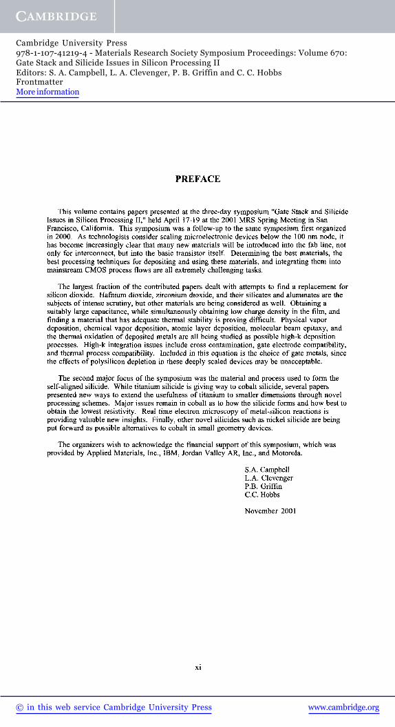
PREFACE
This volume contains papers presented at the three-day symposium "Gate Stack and SilicideIssues in Silicon Processing II," held April 17-19 at the 2001 MRS Spring Meeting in SanFrancisco, California. This symposium was a follow-up to the same symposium first organizedin 2000. As technologists consider scaling microelectronic devices below the 100 nm node, ithas become increasingly clear that many new materials will be introduced into the fab line, notonly for interconnect, but into the basic transistor itself. Determining the best materials, thebest processing techniques for depositing and using these materials, and integrating them intomainstream CMOS process flows are all extremely challenging tasks.
The largest fraction of the contributed papers dealt with attempts to find a replacement forsilicon dioxide. Hafnium dioxide, zirconium dioxide, and their silicates and aluminates are thesubjects of intense scrutiny, but other materials are being considered as well. Obtaining asuitably large capacitance, while simultaneously obtaining low charge density in the film, andfinding a material that has adequate thermal stability is proving difficult. Physical vapordeposition, chemical vapor deposition, atomic layer deposition, molecular beam epitaxy, andthe thermal oxidation of deposited metals are all being studied as possible high-k depositionprocesses. High-k integration issues include cross contamination, gate electrode compatibility,and thermal process compatibility. Included in this equation is the choice of gate metals, sincethe effects of poly silicon depletion in these deeply scaled devices may be unacceptable.
The second major focus of the symposium was the material and process used to form theself-aligned silicide. While titanium silicide is giving way to cobalt silicide, several paperspresented new ways to extend the usefulness of titanium to smaller dimensions through novelprocessing schemes. Major issues remain in cobalt as to how the silicide forms and how best toobtain the lowest resistivity. Real time electron microscopy of metal-silicon reactions isproviding valuable new insights. Finally, other novel silicides such as nickel silicide are beingput forward as possible alternatives to cobalt in small geometry devices.
The organizers wish to acknowledge the financial support of this symposium, which wasprovided by Applied Materials, Inc., IBM, Jordan Valley AR, Inc., and Motorola.
S.A. CampbellL.A. ClevengerP.B. GriffinC.C. Hobbs
November 2001
www.cambridge.org© in this web service Cambridge University Press
Cambridge University Press978-1-107-41219-4 - Materials Research Society Symposium Proceedings: Volume 670:Gate Stack and Silicide Issues in Silicon Processing IIEditors: S. A. Campbell, L. A. Clevenger, P. B. Griffin and C. C. HobbsFrontmatterMore information
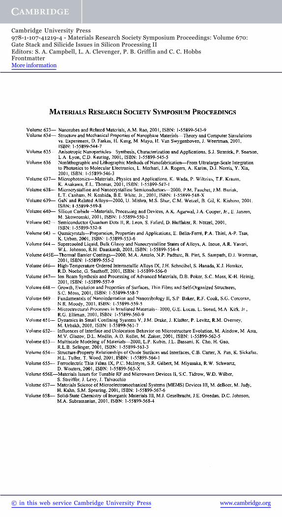
MATERIALS RESEARCH SOCIETY SYMPOSIUM PROCEEDINGS
Volume 633— Nanotubes and Related Materials, A.M. Rao, 2001, ISBN: 1-55899-543-9Volume 634— Structure and Mechanical Properties of Nanophase Materials—Theory and Computer Simulations
vs. Experiment, D. Farkas, H. Kung, M. Mayo, H. Van Swygenhoven, J. Weertman, 2001,ISBN: 1-55899-544-7
Volume 635— Anisotropic Nanoparticles—Synthesis, Characterization and Applications, S.J. Stranick, P. Searson,L.A. Lyon, CD. Keating, 2001, ISBN: 1-55899-545-5
Volume 636— Nonlithographic and Lithographic Methods of Nanofabrication—From Ultralarge-Scale Integrationto Photonics to Molecular Electronics, L. Merhari, J.A. Rogers, A. Karim, D.J. Norris, Y. Xia,2001, ISBN: 1-55899-546-3
Volume 637— Microphotonics—Materials, Physics and Applications, K. Wada, P. Wiltzius, T.F. Krauss,K. Asakawa, EL. Thomas, 2001, ISBN: 1-55899-547-1
Volume 638— Microcrystalline and Nanocrystalline Semiconductors—2000, P.M. Fauchet, J.M. Buriak,L.T. Canham, N. Koshida, B.E. White, Jr., 2001, ISBN: 1-55899-548-X
Volume 639— GaN and Related Alloys—2000, U. Mishra, M.S. Shur, CM. Wetzel, B. Gil, K. Kishino, 2001.ISBN: 1-55899-549-8
Volume 640— Silicon Carbide—Materials, Processing and Devices, A.K. Agarwal, J.A. Cooper, Jr., E. Janzen,M. Skowronski, 2001, ISBN: 1-55899-550-1
Volume 642— Semiconductor Quantum Dots II, R. Leon, S. Fafard, D. Huffaker, R. Notzel, 2001,ISBN: 1-55899-552-8
Volume 643— Quasicyrstals—Preparation, Properties and Applications, E. Belin-Ferre, P.A. Thiel, A-P. Tsai,K. Urban, 2001, ISBN: 1-55899-553-6
Volume 644— Supercooled Liquid, Bulk Glassy and Nanocrystalline States of Alloys, A. Inoue, A.R. Yavari,W.L. Johnson, R.H. Dauskardt, 2001, ISBN: 1-55899-554-4
Volume 645E—Thermal Barrier Coatings—2000, M.A. Antelo, N.P. Padture, B. Pint, S. Sampath, D.J. Wortman,2001, ISBN: 1-55899-555-2
Volume 646— High-Temperature Ordered Intermetallic Alloys IX, J.H. Schneibel, S. Hanada, K.J. Hemker,R.D. Noebe, G. Sauthoff, 2001, ISBN: 1-55899-556-0
Volume 647— Ion Beam Synthesis and Processing of Advanced Materials, D.B. Poker, S.C. Moss, K-H. Heinig,2001, ISBN: 1-55899-557-9
Volume 648— Growth, Evolution and Properties of Surfaces, Thin Films and Self-Organized Structures,S.C. Moss, 2001, ISBN: 1-55899-558-7
Volume 649— Fundamentals of Nanoindentation and Nanotribology II, S.P. Baker, R.F. Cook, S.G. Corcoran,N.R. Moody, 2001, ISBN: 1-55899-559-5
Volume 650— Microstructural Processes in Irradiated Materials—2000, G.E. Lucas, L. Snead, M.A. Kirk. Jr.,R.G. Elliman, 2001, ISBN: 1-55899-560-9
Volume 651— Dynamics in Small Confining Systems V, J.M. Drake, J. Klafter, P. Levitz, R.M. Overney,M. Urbakh, 2001, ISBN: 1-55899-561-7
Volume 652— Influences of Interface and Dislocation Behavior on Microstructure Evolution, M. Aindow, M. Asta,M.V. Glazov, D.L. Medlin, A.D. Rollet, M. Zaiser, 2001, ISBN: 1-55899-562-5
Volume 653— Multiscale Modeling of Materials—2000, L.P. Kubin, J.L. Bassani, K. Cho, H. Gao,R.L.B. Selinger, 2001, ISBN: 1-55899-563-3
Volume 654— Structure-Property Relationships of Oxide Surfaces and Interfaces, C.B. Carter, X. Pan, K. Sickafus,H.L. Tuller, T. Wood, 2001, ISBN: 1-55899-564-1
Volume 655— Ferroelectric Thin Films IX, P.C Mclntyre, S.R. Gilbert, M. Miyasaka, R.W. Schwartz,D. Wouters, 2001, ISBN: 1-55899-565-X
Volume 656E—Materials Issues for Tunable RF and Microwave Devices II, S.C Tidrow, W.D. Wilber,S. Streiffer, J. Levy, J. Talvacchio
Volume 657— Materials Science of Microelectromechanical Systems (MEMS) Devices III, M. deBoer, M. Judy,H. Kahn, S.M. Spearing, 2001, ISBN: 1-55899-567-6
Volume 658— Solid-State Chemistry of Inorganic Materials III, M.J. Geselbracht, J.E. Greedan, D.C. Johnson,M.A. Subramanian, 2001, ISBN: 1-55899-568-4
www.cambridge.org© in this web service Cambridge University Press
Cambridge University Press978-1-107-41219-4 - Materials Research Society Symposium Proceedings: Volume 670:Gate Stack and Silicide Issues in Silicon Processing IIEditors: S. A. Campbell, L. A. Clevenger, P. B. Griffin and C. C. HobbsFrontmatterMore information
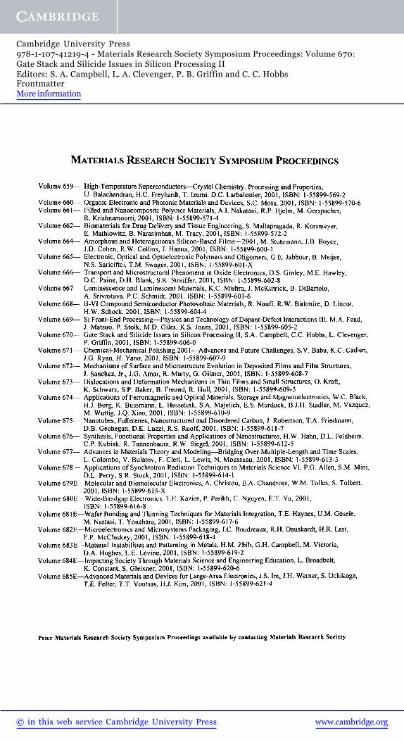
MATERIALS RESEARCH SOCIETY SYMPOSIUM PROCEEDINGS
Volume 659— High-Temperature Superconductors—Crystal Chemistry, Processing and Properties,U. Balachandran, H.C. Freyhardt, T. Izumi, D.C. Larbalestier, 2001, ISBN: 1-55899-569-2
Volume 660— Organic Electronic and Photonic Materials and Devices, S.C. Moss, 2001, ISBN: 1-55899-570-6Volume 661— Filled and Nanocomposite Polymer Materials, A.I. Nakatani, R.P. Hjelm, M. Gerspacher,
R. Krishnamoorti, 2001, ISBN: 1-55899-571-4Volume 662— Biomaterials for Drug Delivery and Tissue Engineering, S. Mallapragada, R. Korsmeyer,
E. Mathiowitz, B. Narasimhan, M. Tracy, 2001, ISBN: 1-55899-572-2Volume 664— Amorphous and Heterogeneous Silicon-Based Films—2001, M. Stutzmann, J.B. Boyce,
J.D. Cohen, R.W. Collins, J. Hanna, 2001, ISBN: 1-55899-600-1Volume 665— Electronic, Optical and Optoelectronic Polymers and Oligomers, G.E. Jabbour, B. Meijer,
N.S. Sariciftci, T.M. Swager, 2001, ISBN: 1-55899-601-XVolume 666— Transport and Microstructural Phenomena in Oxide Electronics, D.S. Ginley, M.E. Hawley,
D.C. Paine, D.H. Blank, S.K. Streiffer, 2001, ISBN: 1-55899-602-8Volume 667— Luminescence and Luminescent Materials, K.C. Mishra, J. McKittrick, B. DiBartolo,
A. Srivastava, P.C. Schmidt, 2001, ISBN: 1-55899-603-6Volume 668— II-VI Compound Semiconductor Photovoltaic Materials, R. Noufi, R.W. Birkmire, D. Lincot,
H.W. Schock, 2001, ISBN: 1-55899-604-4Volume 669— Si Front-End Processing—Physics and Technology of Dopant-Defect Interactions III, M.A. Foad,
J. Matsuo, P. Stolk, M.D. Giles, K.S. Jones, 2001, ISBN: 1-55899-605-2Volume 670— Gate Stack and Silicide Issues in Silicon Processing II, S.A. Campbell, C.C. Hobbs, L. Clevenger,
P. Griffin, 2001, ISBN: 1-55899-606-0Volume 671— Chemical-Mechanical Polishing 2001—Advances and Future Challenges, S.V. Babu, K.C. Cadien,
J.G. Ryan, H. Yano, 2001, ISBN: 1-55899-607-9Volume 672— Mechanisms of Surface and Microstrucure Evolution in Deposited Films and Film Structures,
J. Sanchez, Jr., J.G. Amar, R. Murty, G. Gilmer, 2001, ISBN: 1-55899-608-7Volume 673— Dislocations and Deformation Mechanisms in Thin Films and Small Structures, O. Kraft,
K. Schwarz, S.P. Baker, B. Freund, R. Hull, 2001, ISBN: 1-55899-609-5Volume 674— Applications of Ferromagnetic and Optical Materials, Storage and Magnetoelectronics, W.C. Black,
H.J. Borg, K. Bussmann, L. Hesselink, S.A. Majetich, E.S. Murdock, B.J.H. Stadler, M. Vazquez,M. Wuttig, J.Q. Xiao, 2001, ISBN: 1-55899-610-9
Volume 675— Nanotubes, Fullerenes, Nanostructured and Disordered Carbon, J. Robertson, T.A. Friedmann,D.B. Geohegan, D.E. Luzzi, R.S. Ruoff, 2001, ISBN: 1-55899-611-7
Volume 676— Synthesis, Functional Properties and Applications of Nanostructures, H.W. Hahn, D.L. Feldheim,C.P. Kubiak, R. Tannenbaum, R.W. Siegel, 2001, ISBN: 1-55899-612-5
Volume 677— Advances in Materials Theory and Modeling—Bridging Over Multiple-Length and Time Scales,L. Colombo, V. Bulatov, F. Cleri, L. Lewis, N. Mousseau, 2001, ISBN: 1-55899-613-3
Volume 678— Applications of Synchrotron Radiation Techniques to Materials Science VI, P.G. Allen, S.M. Mini,D.L. Perry, S.R. Stock, 2001, ISBN: 1-55899-614-1
Volume 679E—Molecular and Biomolecular Electronics, A. Christou, E.A. Chandross, W.M. Tolles, S. Tolbert2001, ISBN: 1-55899-615-X
Volume 680E—Wide-Bandgap Electronics, T.E. Kazior, P. Parikh, C. Nguyen, E.T. Yu, 2001,ISBN: 1-55899-616-8
Volume 68IE—Wafer Bonding and Thinning Techniques for Materials Integration, T.E. Haynes, U.M. Gosele,M. Nastasi, T. Yonehara, 2001, ISBN: 1-55899-617-6
Volume 682E—Microelectronics and Microsystems Packaging, J.C. Boudreaux, R.H. Dauskardt, H.R. Last,F.P. McCluskey, 2001, ISBN: 1-55899-618-4
Volume 683E—Material Instabilities and Patterning in Metals, H.M. Zbib, G.H. Campbell, M. Victoria,D.A. Hughes, L.E. Levine, 2001, ISBN: 1-55899-619-2
Volume 684E—Impacting Society Through Materials Science and Engineering Education, L. Broadbelt,K. Constant, S. Gleixner, 2001, ISBN: 1-55899-620-6
Volume 685E—Advanced Materials and Devices for Large-Area Electronics, J.S. Im, J.H. Werner, S. Uchikoga,T.E. Felter, T.T. Voutsas, H.J. Kim, 2001, ISBN: 1-55899-621-4
Prior Materials Research Society Symposium Proceedings available by contacting Materials Research Society
www.cambridge.org© in this web service Cambridge University Press
Cambridge University Press978-1-107-41219-4 - Materials Research Society Symposium Proceedings: Volume 670:Gate Stack and Silicide Issues in Silicon Processing IIEditors: S. A. Campbell, L. A. Clevenger, P. B. Griffin and C. C. HobbsFrontmatterMore information