improvement of thermal stability of ni silicide on heavily ... · improvement of thermal stability...
TRANSCRIPT
1
Master Thesis
Improvement of Thermal Stability of Ni Silicide on Heavily Doped N+-Si
Supervisor
Professor Hiroshi Iwai
Iwai Laboratory
Department of Electronics and Applied Physics
Tokyo Institute of Technology
05M36269
Takashi Shiozawa
2
LIST OF CONTENT Index ............................................................................................ 2
Chapter 1 INTRODUCTION .................................................................... 5
1 Background of this study ............................................................... 6
1.1 Low-Resistivity Materials for Nanoscale CMOS ......................... 9
1.2 Transition of Silicide Technology ............................................... 11
1.3 Comparison of Silicide Materials ................................................ 12
1.4 Purpose of This Study ................................................................. 16
Chapter 2 FABRICATION AND MEASUREMENTS ...................... 18
2 Flow of Experiments .................................................................. 19
2.1 Si Substrate Cleaning Process ..................................................... 19
2.2 UHV Sputtering System .............................................................. 20
2.3 Infrared Annealing Furnace ........................................................ 22
2.4 Four-point Probe Technique ....................................................... 24
2.5 Atomic Force Microscopy (AFM) .............................................. 26
2.6 Scannin Electron Microscope (SEM) ......................................... 27
2.7 X-ray Diffraction (XRD) ............................................................ 27
2.8 Auger Electron Spectroscopy ..................................................... 28
3
Chapter 3 EXPRIMENT RESULTS ......................................................... 30
3.1 Experimental results of pure Ni silicide ...................................... 31
3.1.1 Fabrication process of Ni silicide ............................................. 31
3.1.2 Characteristics of pure Ni silicide …..….................................. 33
3.2 Experimental results of Ni silicide with Al layer ........................ 40
3.2.1 Fabrication process of Ni silicide with Al layer ....................... 40
3.2.2 Characteristics of Ni silicide with Al layer .............................. 41
3.3 Experimental results of Ni silicide
with Al interlayer using TEG wafer .................. 52
3.3.1 Fabrication process of Ni silicide
with Al interlayer on TEG wafer ....................... 52
3.3.2 Characteristics of Ni silicide
with Al layer on TEG wafer .............................. 53
3.4 Experimental results of Ni silicide
with other metal layers ...................................... 60
3.4.1 Characteristics of Ni silicide with other metal layer ................ 60
4
Chapter 4 CONCLUSIONS .................................................................... 60
4.1 Results of This Study ........................................................... 61
4.2 Future Issues ......................................................................... 62
Acknowledgements ............................................................... 63
References ............................................................................... 65

5
Chapter 1
INTRODUCTION
6
1. Background of This Study
About a half century ago, Brattain, Bardeen and Shockley succeeded in inventing
the first transistor. Then, an integrated circuit (IC) is made by killby in 1948. After the
invention of the IC, the number of transistors included in a chip have increased
according to Moore’s law and the semiconductor technologies have accomplished
wonderful development.
CMOS (Complementary Metal Oxide Semiconductor) technology evolution in the
past years has followed the path of device scaling for achieving density, speed, and
power improvements. MOSFET (Metal Oxide Semiconductor Field-Effect Transistor)
scaling was propelled by the rapid advancement of lithographic techniques for
delineating fine lines of 1µm width and below.
In constant-field scaling, it was proposed that one can keep short-channel effects
under control by scaling down the vertical dimensions (gate insulator thickness,
junction depth, etc.) along with the horizontal dimensions, while also proportionally
decreasing the applied voltages and increasing the substrate doping concentration
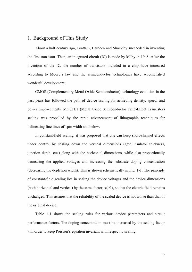
(decreasing the depletion width). This is shown schematically in Fig. 1-1. The principle
of constant-field scaling lies in scaling the device voltages and the device dimensions
(both horizontal and vertical) by the same factor, κ(>1), so that the electric field remains
unchanged. This assures that the reliability of the scaled device is not worse than that of
the original device.
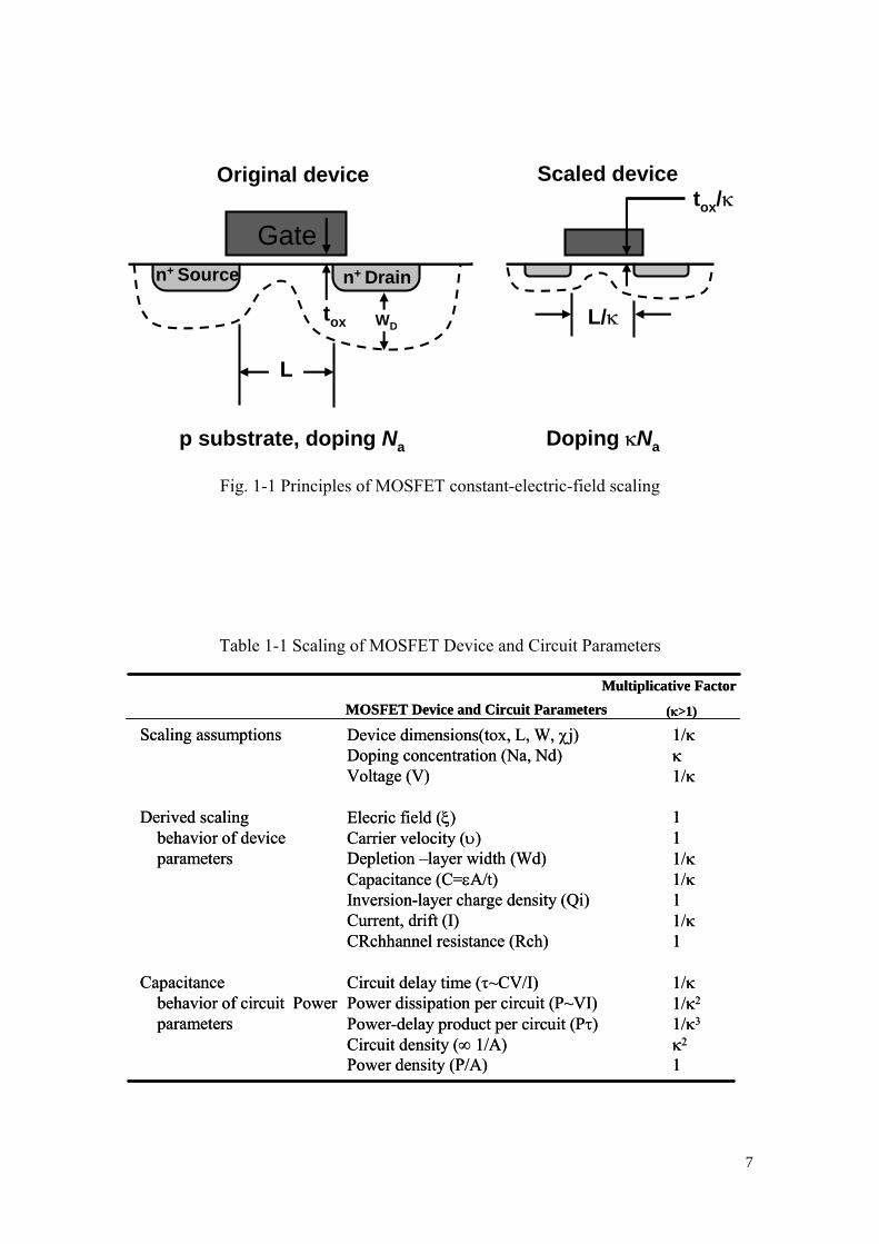
Table 1-1 shows the scaling rules for various device parameters and circuit
performance factors. The doping concentration must be increased by the scaling factor
κ in order to keep Poisson’s equation invariant with respect to scaling.
7
L
n+ Source n+ Drain
Gate
tox WD L/κ
tox/κOriginal device Scaled device
p substrate, doping Na Doping κNa
Fig. 1-1 Principles of MOSFET constant-electric-field scaling
Table 1-1 Scaling of MOSFET Device and Circuit Parameters
Scaling assumptions
Derived scalingbehavior of deviceparameters
Capacitancebehavior of circuit Power parameters
Device dimensions(tox, L, W, χj)Doping concentration (Na, Nd)Voltage (V)
Elecric field (ξ) Carrier velocity (υ) Depletion –layer width (Wd) Capacitance (C=εA/t)Inversion-layer charge density (Qi) Current, drift (I) CRchhannel resistance (Rch)
Circuit delay time (τ~CV/I)Power dissipation per circuit (P~VI) Power-delay product per circuit (Pτ) Circuit density (∞ 1/A) Power density (P/A)
1/κκ1/κ
111/κ1/κ11/κ1
1/κ1/κ2
1/κ3
κ2
1
MOSFET Device and Circuit ParametersMultiplicative Factor
(κ>1)
8
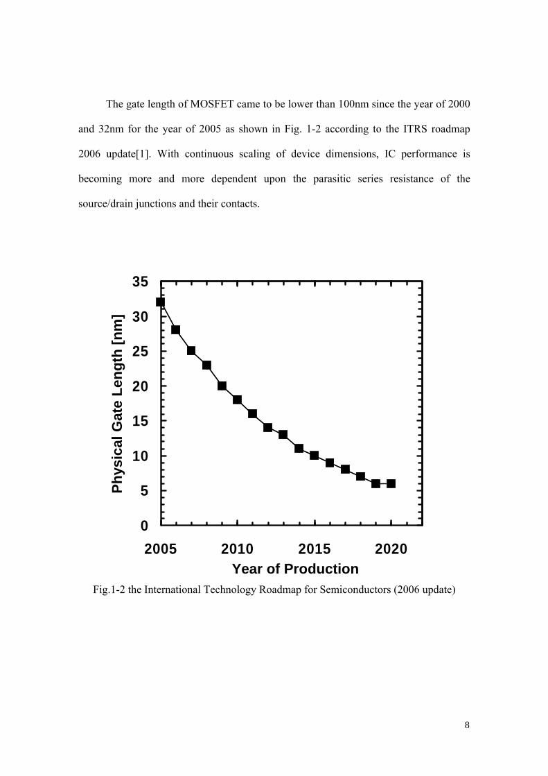
The gate length of MOSFET came to be lower than 100nm since the year of 2000
and 32nm for the year of 2005 as shown in Fig. 1-2 according to the ITRS roadmap
2006 update[1]. With continuous scaling of device dimensions, IC performance is
becoming more and more dependent upon the parasitic series resistance of the
source/drain junctions and their contacts.
0
5
10
15
20
25
30
35
2005 2010 2015 2020
Phys
ical
Gat
e Le
ngth
[nm
]
Year of Production Fig.1-2 the International Technology Roadmap for Semiconductors (2006 update)
9
1.1 Low-Resistivity Materials for Nanoscale CMOS
The primary thrust of very large scale integration (VLSI) has resulted in devices
that are smaller and faster and that consume less power. The continued evolution of
smaller and smaller devices has aroused a renewed interest in the development of new
metallization schemes for low-resistivity gates, interconnections, and ohmic contacts.
This is interest in new metallization arose because as the device sizes are scaled down,
the linewidth gets narrower and the sheet resistance contribution to the RC delay
increases.
The conventional polysilicon whose sheet resistance is about 30 to 60 Ω/sq, is too
high to be applied to modern VLSI. Aluminum, tungsten, and molybdenum are notable
among the metals proposed for gate and interconnect metallization. The use of
aluminum, however, requires all postgate processing of the devices to be limited to
very low temperatures, preferably below 500oC. The use of the refractory metals
tungsten and molybdenum requires complete passivation of these metals from
oxidizing ambients, deposition by means that will not lead to unwanted traps in the
gate oxide, and reliable etching of the metals for pattern generation. The uncertainties
associated with the stability of these metal films have led to search for alternatives.
The silicides have attracted attention because of their low and metal-like
resistivities and their high temperature stability. The use of silicides, with resistivity
about one-tenth of the polysilicon, have greatly improved the speed of the circuits.
Scaling down the size of the device also means reduced junction depths, which
can lead to contact problems. In particular, shallow junctions limit the use of aluminum
due to its known penetration in silicon. Forming silicides in the contact windows by

10
reaction between the silicon substrate and a thin metal layer offers a possibility of
forming contacts with lower contanct resistances.
(A) (B)
(C) (D)
(A) (B)
(C) (D)
MetalPoly-Si
Silicide
(A) (B)
(C) (D)
(A) (B)
(C) (D)
Fig.1- Self-Align Silicide (SALICIDE) Process. (A) Conventional MOSFET before Metallization. (B) After Metal Deposition.
(C) After RTA for Silicidation. (D)After Selective Etching
11
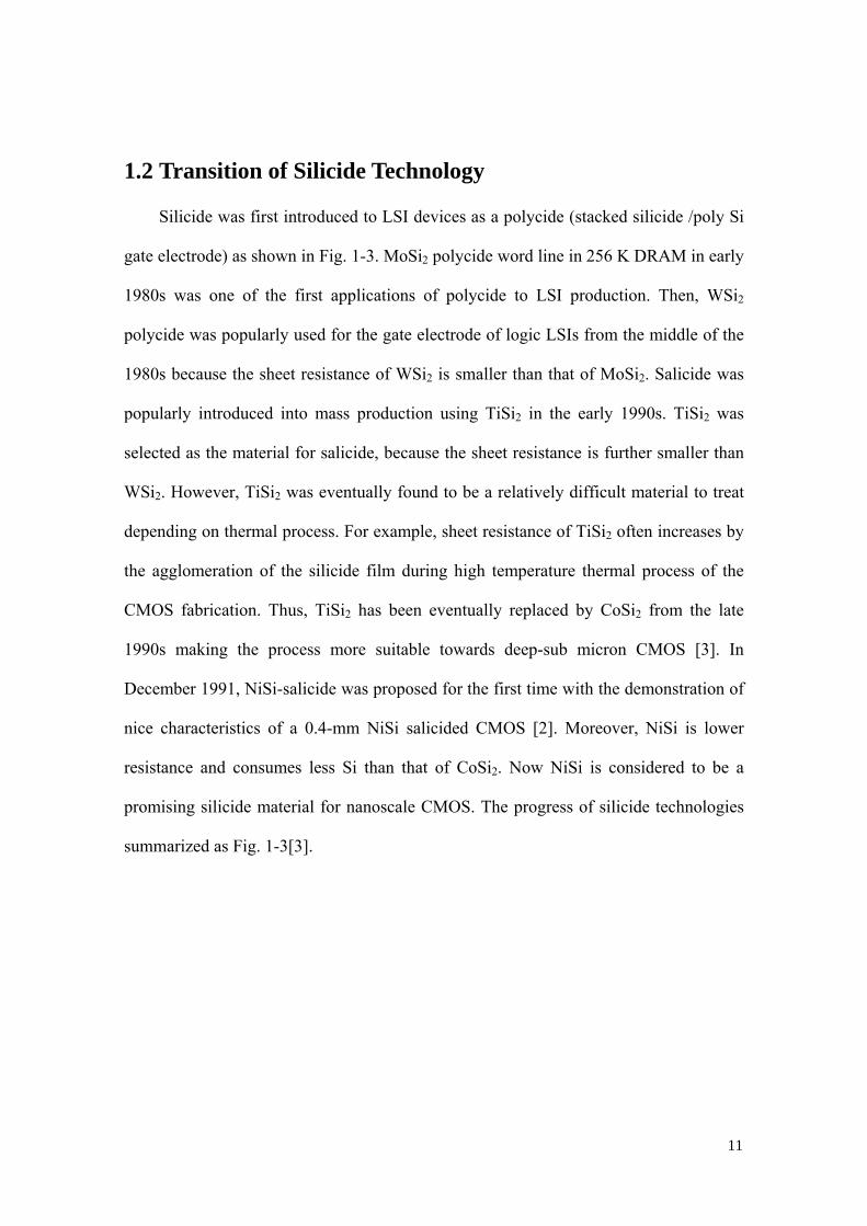
1.2 Transition of Silicide Technology
Silicide was first introduced to LSI devices as a polycide (stacked silicide /poly Si
gate electrode) as shown in Fig. 1-3. MoSi2 polycide word line in 256 K DRAM in early
1980s was one of the first applications of polycide to LSI production. Then, WSi2
polycide was popularly used for the gate electrode of logic LSIs from the middle of the
1980s because the sheet resistance of WSi2 is smaller than that of MoSi2. Salicide was
popularly introduced into mass production using TiSi2 in the early 1990s. TiSi2 was
selected as the material for salicide, because the sheet resistance is further smaller than
WSi2. However, TiSi2 was eventually found to be a relatively difficult material to treat
depending on thermal process. For example, sheet resistance of TiSi2 often increases by
the agglomeration of the silicide film during high temperature thermal process of the
CMOS fabrication. Thus, TiSi2 has been eventually replaced by CoSi2 from the late
1990s making the process more suitable towards deep-sub micron CMOS [3]. In
December 1991, NiSi-salicide was proposed for the first time with the demonstration of
nice characteristics of a 0.4-mm NiSi salicided CMOS [2]. Moreover, NiSi is lower
resistance and consumes less Si than that of CoSi2. Now NiSi is considered to be a
promising silicide material for nanoscale CMOS. The progress of silicide technologies
summarized as Fig. 1-3[3].
12
Fig. 1-3 Progress of silicate materials
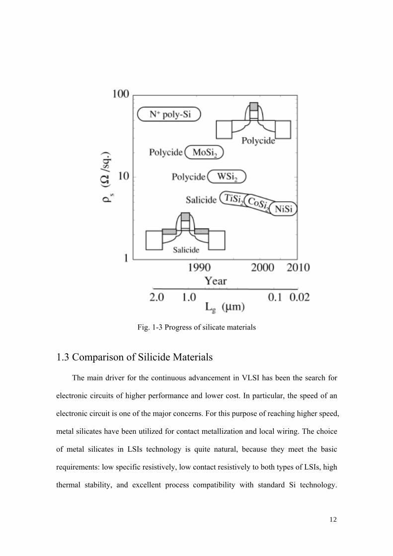
1.3 Comparison of Silicide Materials
The main driver for the continuous advancement in VLSI has been the search for
electronic circuits of higher performance and lower cost. In particular, the speed of an
electronic circuit is one of the major concerns. For this purpose of reaching higher speed,
metal silicates have been utilized for contact metallization and local wiring. The choice
of metal silicates in LSIs technology is quite natural, because they meet the basic
requirements: low specific resistively, low contact resistively to both types of LSIs, high
thermal stability, and excellent process compatibility with standard Si technology.
13
Today, metal silicides are an inseparable part of an electronic device. Here are some
comparisons about silicide materials. Fig. 1-4 shows the dependence of sheet resistance
on line width for various silicide materials. Ni silicide possesses not only the lowest
sheet resistance but also the best width independence among TiSi2(Conventional
process), TiSi2(Pre-amorphization) and CoSi2 as well.
Fig. 1-4 Dependence of sheet resistance on line width for various silicide materials
14
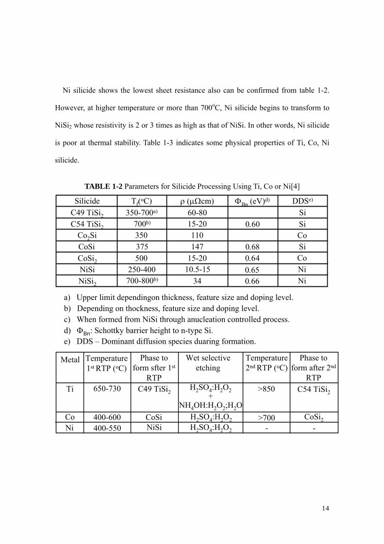
Ni silicide shows the lowest sheet resistance also can be confirmed from table 1-2.
However, at higher temperature or more than 700oC, Ni silicide begins to transform to
NiSi2 whose resistivity is 2 or 3 times as high as that of NiSi. In other words, Ni silicide
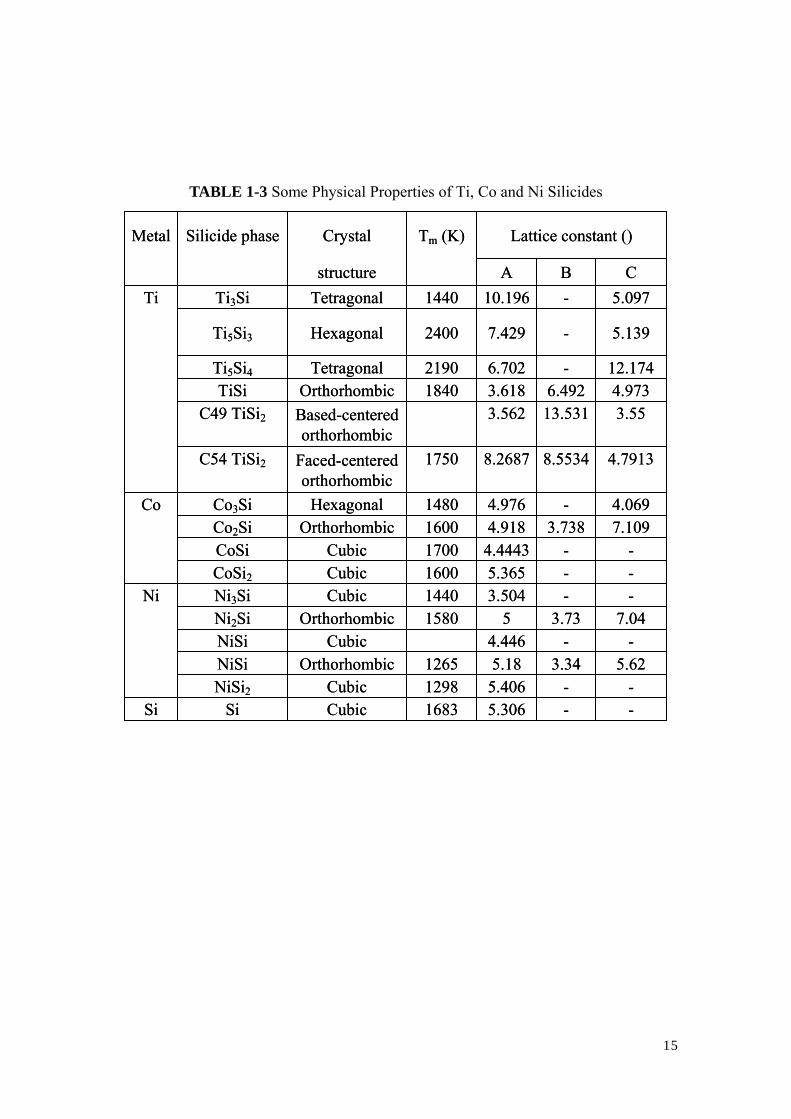
is poor at thermal stability. Table 1-3 indicates some physical properties of Ti, Co, Ni
silicide.
TABLE 1-2 Parameters for Silicide Processing Using Ti, Co or Ni[4]
SilicideC49 TiSi2
C54 TiSi2Co2Si
CoSi2NiSiNiSi2
Tf(oC)
CoSi
350-700a)
700b)
700-800b)250-400
500375350
ρ (µΩcm)60-8015-20110147
15-2010.5-15
34
ΦBn (eV)d)
0.60
0.680.640.650.66
DDSe)
SiSi
SiCo
CoNiNi
a) Upper limit dependingon thickness, feature size and doping level.b) Depending on thockness, feature size and doping level.c) When formed from NiSi through anucleation controlled process.d) ΦBn: Schottky barrier height to n-type Si.e) DDS – Dominant diffusion species duaring formation.
Metal Temperature1st RTP (oC)
Phase to form sfter 1st
RTP
Wet selective etching
Temperature2nd RTP (oC)
Phase to form after 2nd
RTPTi
CoNi
650-730 C49 TiSi2
400-600400-550
CoSiNiSi
H2SO4:H2O2+
NH4OH:H2O2;H2OH2SO4:H2O2H2SO4:H2O2
>850
>700-
C54 TiSi2
CoSi2
-
15
TABLE 1-3 Some Physical Properties of Ti, Co and Ni Silicides
--5.3061683CubicSiSi--5.4061298CubicNiSi2
5.623.345.181265OrthorhombicNiSi--4.446CubicNiSi
7.043.7351580OrthorhombicNi2Si--3.5041440CubicNi3SiNi--5.3651600CubicCoSi2
--4.44431700CubicCoSi7.1093.7384.9181600OrthorhombicCo2Si4.069-4.9761480HexagonalCo3SiCo
4.79138.55348.26871750Faced-centeredorthorhombic
C54 TiSi2
3.5513.5313.562Based-centeredorthorhombic
C49 TiSi2
4.9736.4923.6181840OrthorhombicTiSi12.174-6.7022190TetragonalTi5Si4
5.139-7.4292400HexagonalTi5Si3
5.097-10.1961440TetragonalTi3SiTiCBAstructure
Lattice constant ()Tm (K)Crystal Silicide phaseMetal
16
1.4 Purpose of This Study
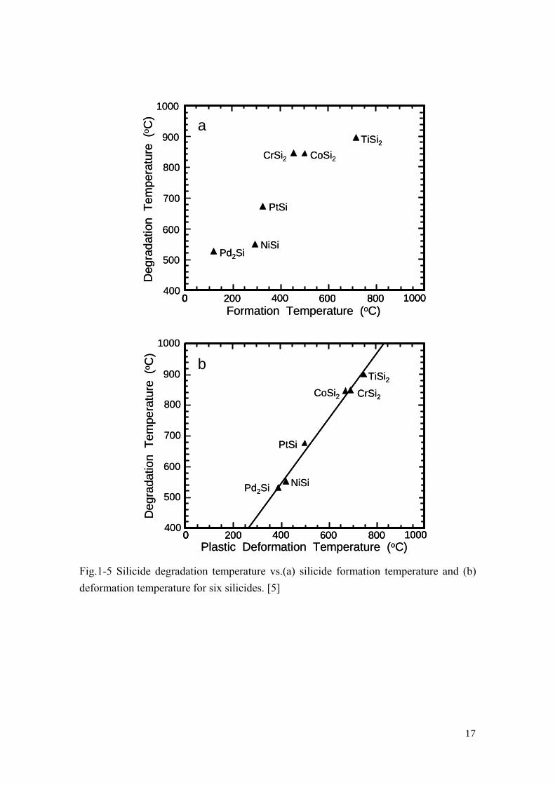
As mentioned in section 1.3, the thermal stability of Ni silicide is very poor.
Compared with other silicide materials as shown in Fig. 1-5, Ni silicide is so sensible to
heat that its degradation temperature is only 500-600oC. Ni silicide forms at about
350oC and turns to be a high resistance material called NiSi2 at the temperature of about
700 oC on P-type Si. While the thermal stability of Ni silicide on heavily doped N+
substrates with As concentration of ~1020/cm3, whose density is expected for the 45nm
node exhibited considerable degradation compared with that on the P+ substrates to
mention it later. Thus, the purpose of this study is to find out the method to improve the
thermal stability of Ni silicide on heavily doped N+ Si with maintaining quality of
thermal stability the case its method is adopted to P+ heavily doped Si.
17
NiSiPd2Si
PtSi
CoSi2 CrSi2
TiSi2
TiSi2CrSi2 CoSi2
PtSi
NiSiPd2Si
00 200 400 600 800 1000400
500
600
700
800
900
1000
Formation Temperature (oC)
Deg
rada
tion
Tem
pera
ture
(o C
)
00 200 400 600 800 1000400
500
600
700
800
900
1000
Plastic Deformation Temperature (oC)
Deg
rada
tion
Tem
pera
ture
(o C
)
NiSiPd2Si
PtSi
CoSi2 CrSi2
TiSi2
TiSi2CrSi2 CoSi2
PtSi
NiSiPd2Si
00 200 400 600 800 100000 200 400 600 800 1000400
500
600
700
800
900
1000
Formation Temperature (oC)
Deg
rada
tion
Tem
pera
ture
(o C
)
00 200 400 600 800 100000 200 400 600 800 1000400
500
600
700
800
900
1000
Plastic Deformation Temperature (oC)
Deg
rada
tion
Tem
pera
ture
(o C
)
a
b
Fig.1-5 Silicide degradation temperature vs.(a) silicide formation temperature and (b) deformation temperature for six silicides. [5]
18
Chapter 2
FABRICATION AND MEASUREMENTS
19
2 Flow of Experiments
In this chapter, experiment instruments which were used in this study were
introduced. Before these introductions, flow of experiments was presented in brief.
N-type (100)Si substrates with As concentration of ~1020/cm3, whose density is
expected for the 45nm node, were used in this study.
After Si substrate was cleaned by SPM and diluted HF, film structures M/Ni/Si,
Ni/M/Si, Ni/M/Ni/Si(Here M is a metal additive except Ni.) and Ni/Si were deposited
on Si (100) substrates by using an UHV-sputtering system after substrate cleaning
process. Then these samples were annealed in forming gas (N2:H2=97:3) ambient using
a rapid thermal annealing (abbreviated as RTA) system. Sheet resistance of the silicide
layers was measured by the four point probe method. Structures of the layers were
observed by AFM, XRD, AES etc.
2.1 Si Substrate Cleaning Process
At first, high quality thin films require ultra clean Si surface without particle
contamination, metal contamination, organic contamination, ionic contamination, water
absorption, native oxide and atomic scale roughness.
One of the most important chemicals used in Si substrate cleaning is DI
(de-ionized) water. DI water is highly purified and filtered to remove all traces of ionic,
particulate, and bacterial contamination. The theoretical resistivity of pure water is
18.25 MΩcm at 25oC. Ultra-pure water (UPW) system used in this study provided UPW
of more than 18.2 MΩcm at resistivity, fewer than 1 colony of bacteria per milliliter
and fewer than 1 particle (fФ0.1µm) per milliliter.
In this study, the Si substrate was cleaned on a basis of RCA cleaning process,
20
which was proposed by W. Kern et al. But some steps were reduced. The flow of the Si
clean process was shown as Fig.2.1. The first step, which use a solution of sulfuric acid
(H2SO4) / hydrogen peroxide (H2O2) (H2SO4: H2O2=4:1), was performed to remove any
organic material and metallic impurities. After that, the native or chemical oxide was
removed by diluted hydrofluoric acid (HF:H2O=1:99). Then the cleaned wafer was
dipped in DI water. Finally, the cleaned Si substrate was loaded to chamber to deposit
as soon as it was dried by air gun.
2.2 UHV-Sputtering System
After cleaned by chemicals, film structures such as M/Ni/Si, Ni/M/Si (Here M is a
metal additive except Ni.) and Ni/Si were formed by an UHV-sputtering system.
Sputtering is one of the vacuum processes used to deposit ultra thin films on
substrates. It is performed by applying a high voltage across a low-pressure gas
(usually argon at about 5 millitorr)to create a “plasma,” which consists of electrons and
gas ions in a high-energy state. Then the energized plasma ions strike a “target,”
composed of the desired coating material, and cause atoms from that target to be ejected
with enough energy to travel to, and bond with the substrate.
An UHV-sputtering system is used for thin film formations of electronic devices,
for experiments of GMR, and for creating new materials of high temperature
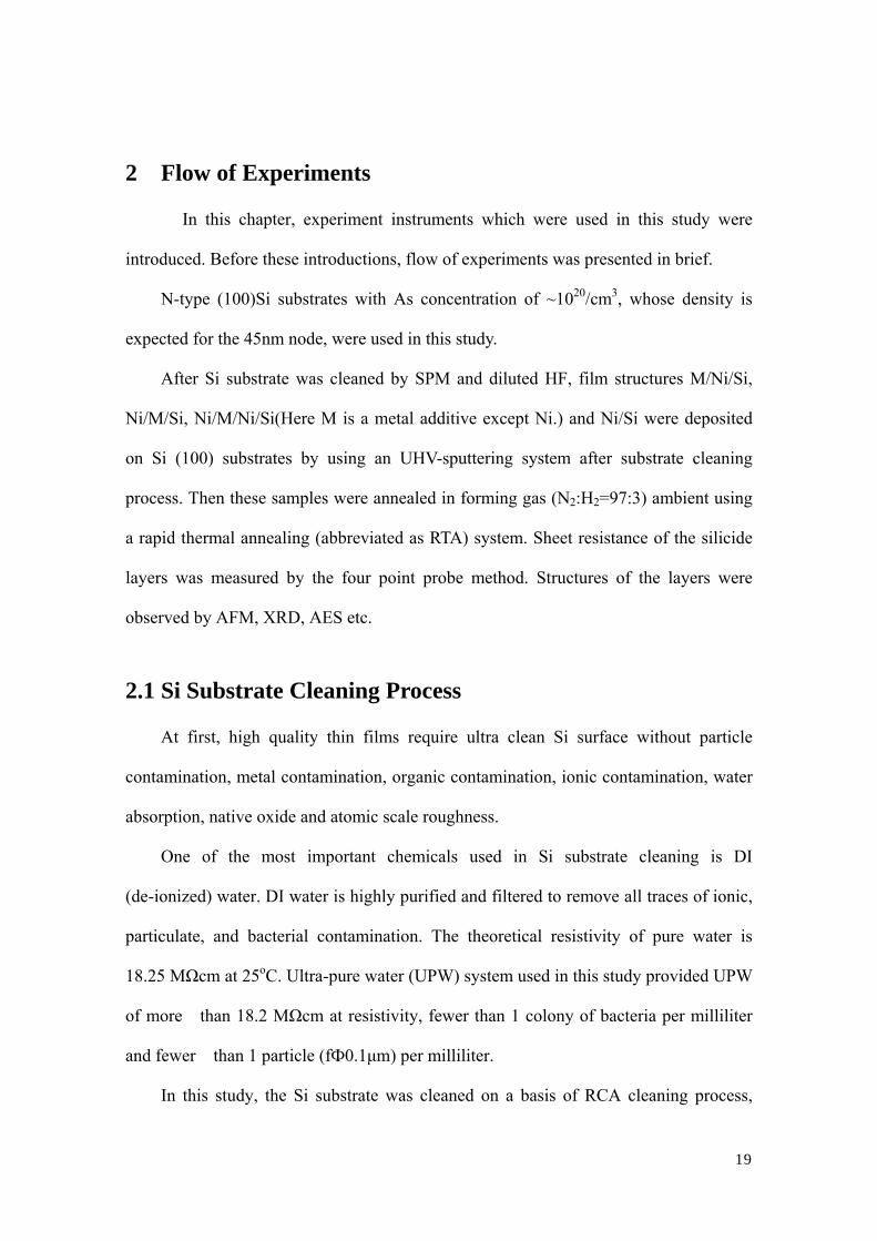
superconductors. In this study, UHV Multi Target Sputtering System ES-350SU
shown as Fig. 2-2 was conducted. The rotating function of target positioning is
developed, enabling this system to sputter 5 targets by means of DC & RF power
sources by using a single electrode. The substrate holder can be rotated and its speed
can be selected. As for other details, Table 2-1 is attached for reference.
21
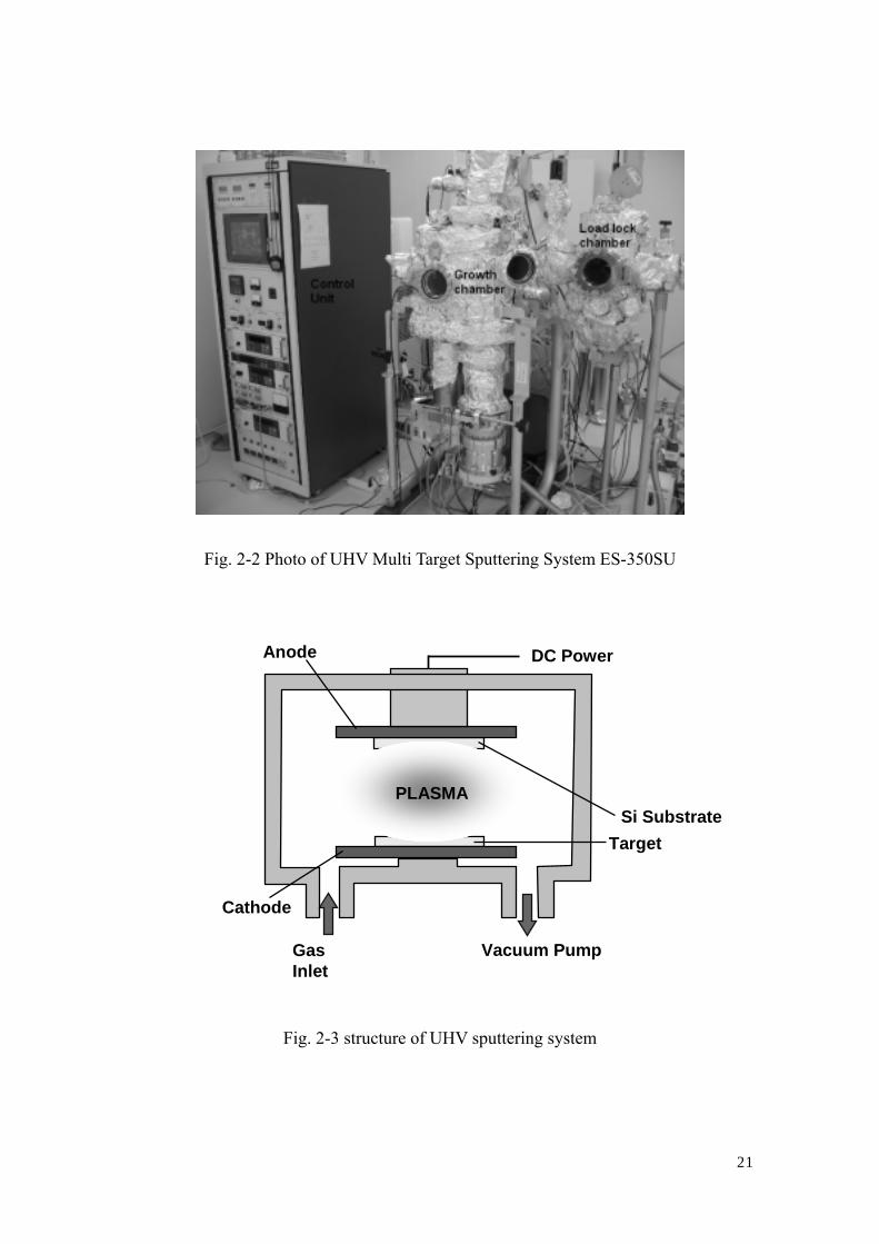
Fig. 2-2 Photo of UHV Multi Target Sputtering System ES-350SU
Vacuum Pump
PLASMASi Substrate
Target
DC PowerAnode
Cathode
Gas Inlet
Fig. 2-3 structure of UHV sputtering system
22
Table 2-1 Specifications for UHV Multi Target Sputtering System ES-350SU
1. Ultimate pressure 1.5 x 10⁻⁶Pa
2. Substrate size 2 inch in diameter
3. Heating temperature 600ºC
4. Heater type Lamp type heater
Growth chamber
5. Target 3 inch x 5 pieces (motor-driven)
6. Vacuum pumps TMP 500L/sec and RP 250L/min
7.Ultimate pressure 6.6 x 10⁻⁵Pa
8. Vacuum pumps
TMP60L/sec and RP90L/min
Load lock chamber
9. Substrate holder with cooling function / Substrate holder with heating function /Cleaning function / Radical beam source
2.3 Infrared Annealing Furnace
After formation from UHV sputtering system, thin films of Ni/Si, Ni/M/Si,
M/Ni/Si were moved to annealing furnace to hold thermal process.
In order to obtain high quality films, annealing process after deposition is required.
The annealing after deposition is considered to bring the suppression of leakage current
because of the defects in the films and surface roughness. In this study, thermal process
leads to the reaction of Ni with Si.
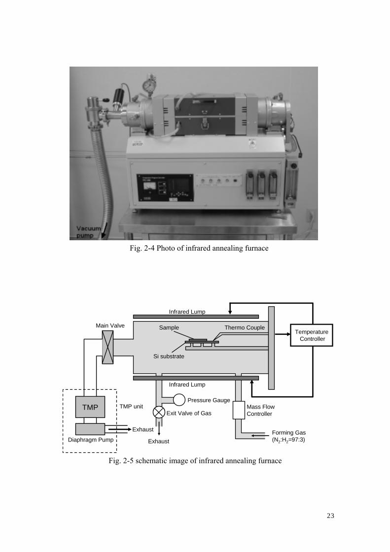
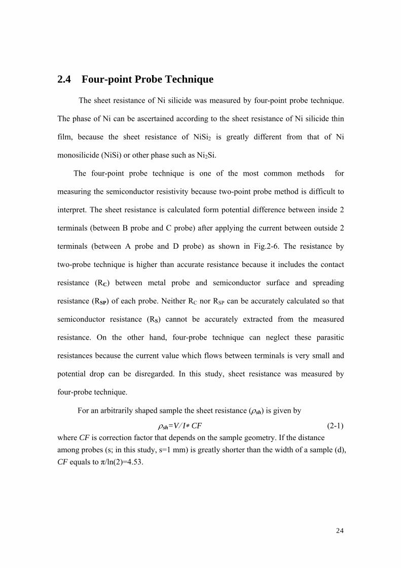
The equipment for annealing used in this investigation was QHC-P610CP
(ULVAC RIKO Co. Ltd). Fig. 2-4 is the photo of the infrared annealing furnace, whose
schematic illustration was shown as Fig. 2-5. The annealing was performed by six
infrared lamps surrounding the sample stage which were made of carbon and coated by
SiC. The heating temperature was controlled by thermocouple feedback.
23
Fig. 2-4 Photo of infrared annealing furnace
TMPTMP
Exhaust
Diaphragm Pump
Thermo CoupleMain Valve
Infrared Lump
Infrared Lump
TemperatureController
TMP unit Mass Flow Controller
Pressure Gauge
Exit Valve of Gas
ExhaustForming Gas (N2:H2=97:3)
Sample
Si substrate
Fig. 2-5 schematic image of infrared annealing furnace
24
2.4 Four-point Probe Technique
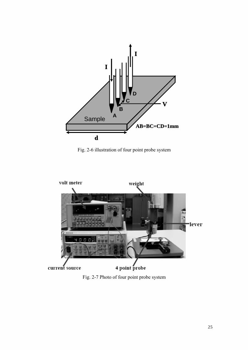
The sheet resistance of Ni silicide was measured by four-point probe technique.
The phase of Ni can be ascertained according to the sheet resistance of Ni silicide thin
film, because the sheet resistance of NiSi2 is greatly different from that of Ni
monosilicide (NiSi) or other phase such as Ni2Si.
The four-point probe technique is one of the most common methods for
measuring the semiconductor resistivity because two-point probe method is difficult to
interpret. The sheet resistance is calculated form potential difference between inside 2
terminals (between B probe and C probe) after applying the current between outside 2
terminals (between A probe and D probe) as shown in Fig.2-6. The resistance by
two-probe technique is higher than accurate resistance because it includes the contact
resistance (RC) between metal probe and semiconductor surface and spreading
resistance (RSP) of each probe. Neither RC nor RSP can be accurately calculated so that
semiconductor resistance (RS) cannot be accurately extracted from the measured
resistance. On the other hand, four-probe technique can neglect these parasitic
resistances because the current value which flows between terminals is very small and
potential drop can be disregarded. In this study, sheet resistance was measured by
four-probe technique.
For an arbitrarily shaped sample the sheet resistance (ρsh) is given by
ρsh=V/ I∗ CF (2-1) where CF is correction factor that depends on the sample geometry. If the distance among probes (s; in this study, s=1 mm) is greatly shorter than the width of a sample (d), CF equals to π/ln(2)=4.53.
25
AB
CD
V
I
I
Sample
d
AB=BC=CD=1mm
AB
CD
V
I
I
Sample
d
AB
CD
V
I
I
Sample
d
AB=BC=CD=1mm
Fig. 2-6 illustration of four point probe system
Fig. 2-7 Photo of four point probe system
26
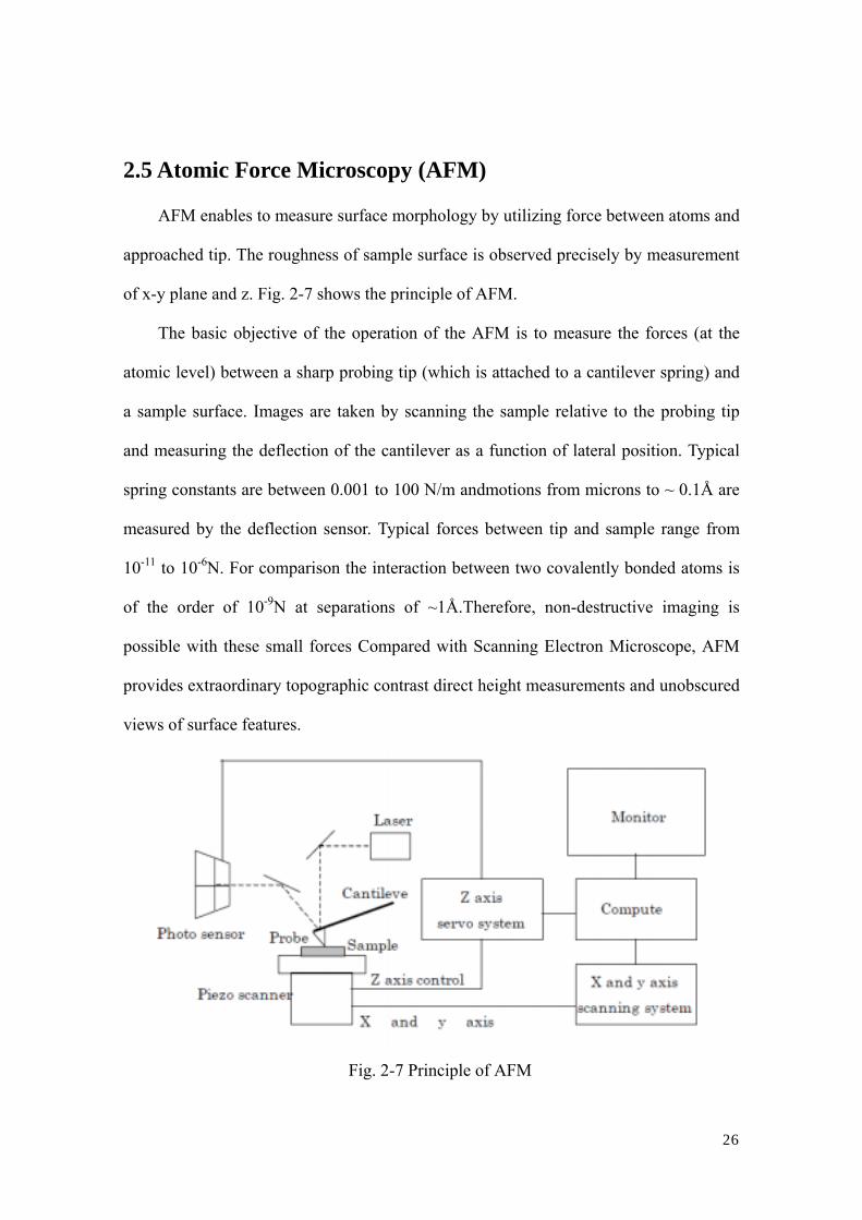
2.5 Atomic Force Microscopy (AFM)
AFM enables to measure surface morphology by utilizing force between atoms and
approached tip. The roughness of sample surface is observed precisely by measurement
of x-y plane and z. Fig. 2-7 shows the principle of AFM.
The basic objective of the operation of the AFM is to measure the forces (at the
atomic level) between a sharp probing tip (which is attached to a cantilever spring) and
a sample surface. Images are taken by scanning the sample relative to the probing tip
and measuring the deflection of the cantilever as a function of lateral position. Typical
spring constants are between 0.001 to 100 N/m andmotions from microns to ~ 0.1Å are
measured by the deflection sensor. Typical forces between tip and sample range from
10-11 to 10-6N. For comparison the interaction between two covalently bonded atoms is
of the order of 10-9N at separations of ~1Å.Therefore, non-destructive imaging is
possible with these small forces Compared with Scanning Electron Microscope, AFM
provides extraordinary topographic contrast direct height measurements and unobscured
views of surface features.
Fig. 2-7 Principle of AFM

27
2.6 Scanning Electron Microscope (SEM)
The Scanning Electron Microscope (SEM) is a microscope that uses electrons
rather than light to form an image. There are many advantages to using the SEM instead
of a light microscope. The SEM has a large depth of field, which allows a large amount
of the sample to be in focus at one time. The SEM also produces images of high
resolution, which means that closely spaced features can be examined at a high
magnification. Preparation of the samples is relatively easy since most SEMs require the
sample to be conductive. The combination of higher magnification, larger depth of
focus, greater resolution, and ease of sample observation makes the SEM one of the
most heavily used instruments in research areas today. The SEM uses electrons instead
of light to form an image. A beam of electrons is produced at the top of the microscope
by heating of a metallic filament. The electron beam follows a vertical path through the
column of the microscope. It makes its way through electromagnetic lenses which focus
and direct the beam down towards the sample. Once it hits the sample, other electrons
(backscattered or secondary) are ejected from the sample. Detectors collect the
secondary or backscattered electrons, and convert them to a signal that is sent to a
viewing screen similar to the one in an ordinary television, producing an image.
2.7 X-ray Diffraction (XRD)
X-ray Diffraction (XRD) is a powerful non-destructive technique for
characterizing crystalline materials. It provides information on structures, phases,
preferred crystal orientations (texture) and other structural parameters such as average
grain size, crystallinity, strain and crystal defects. X-ray diffraction peaks are produced
28
by constructive interference of monochromatic beam scattered from each set of lattice
planes at specific angles. The peak intensities are determined by the atomic decoration
within the lattice planes. Consequently, the X-ray diffraction pattern is the fingerprint of
periodic atomic arrangements in a given material. An on-line search of a standard
database for X-ray powder diffraction pattern enables quick phase identification for a
large variety of crystalline samples.
2.8 Auger Electron Spectroscopy
Auger Electron Spectroscopy (Auger spectroscopy or AES) is a surface specific
technique utilizing the emission of low energy electrons in the Auger process and is one
of the most commonly employed surface analytical techniques for determining the
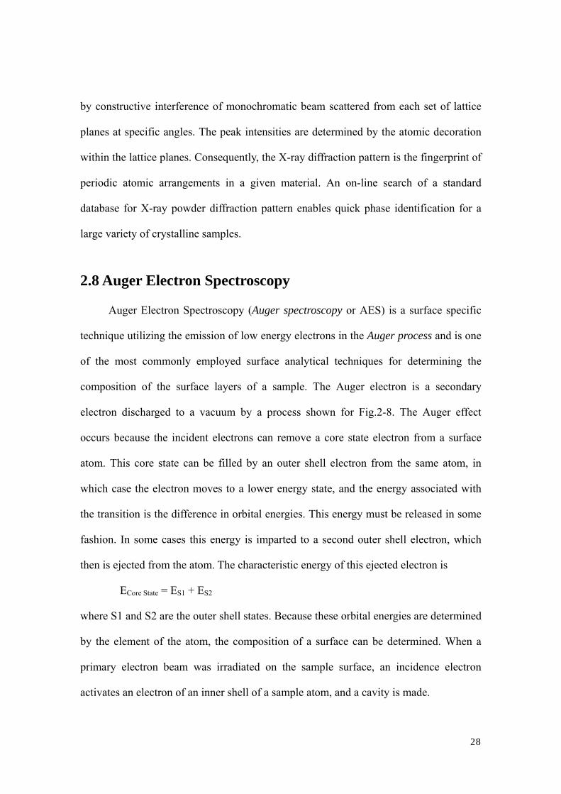
composition of the surface layers of a sample. The Auger electron is a secondary
electron discharged to a vacuum by a process shown for Fig.2-8. The Auger effect
occurs because the incident electrons can remove a core state electron from a surface
atom. This core state can be filled by an outer shell electron from the same atom, in
which case the electron moves to a lower energy state, and the energy associated with
the transition is the difference in orbital energies. This energy must be released in some
fashion. In some cases this energy is imparted to a second outer shell electron, which
then is ejected from the atom. The characteristic energy of this ejected electron is
ECore State = ES1 + ES2
where S1 and S2 are the outer shell states. Because these orbital energies are determined
by the element of the atom, the composition of a surface can be determined. When a
primary electron beam was irradiated on the sample surface, an incidence electron
activates an electron of an inner shell of a sample atom, and a cavity is made.
29
Auger Electron (Ea)Auger Electron (Ea)Primary ElectronPrimary Electron
EnergyEnergy
Fig. 2-8 Principle of AES
30
Chapter 3 EXPERIMENT
RESULTS
31
3.1 Experimental results of pure Ni silicide
In this section, pure Ni silicide was studied to understand its characteristics and
improvement its poor thermal stability. Four kinds of pure Ni silicides (P-type or N-type,
heavily doped or lightly doped) were systemically investigated.
3.1.1 Fabrication process of Ni silicide.
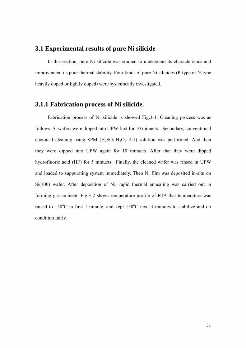
Fabrication process of Ni silicide is showed Fig.3-1. Cleaning process was as
follows. Si wafers were dipped into UPW first for 10 minuets. Secondary, conventional
chemical cleaning using SPM (H2SO4:H2O2=4:1) solution was performed. And then
they were dipped into UPW again for 10 minuets. After that they were dipped
hydrofluoric acid (HF) for 5 minuets. Finally, the cleaned wafer was rinsed in UPW
and loaded to suppurating system immediately. Then Ni film was deposited in-situ on
Si(100) wafer. After deposition of Ni, rapid thermal annealing was carried out in
forming gas ambient. Fig.3-2 shows temperature profile of RTA that temperature was
raised to 150oC in first 1 minute, and kept 150oC next 3 minutes to stabilize and do
condition fairly.
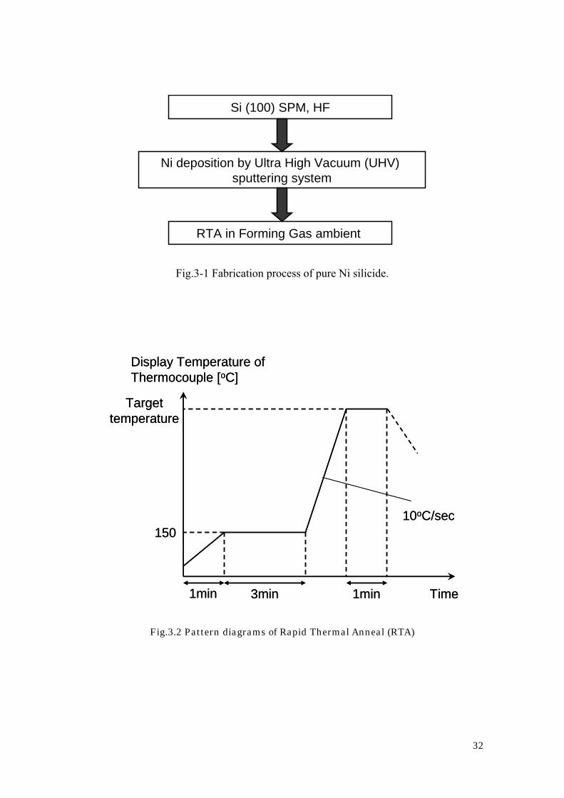
32
Si (100) SPM, HF
Ni deposition by Ultra High Vacuum (UHV) sputtering system
RTA in Forming Gas ambient
Fig.3-1 Fabrication process of pure Ni silicide.
150
Target temperature
1min 3min 1min
10oC/sec
Time
Display Temperature of Thermocouple [oC]
150
Target temperature
1min 3min 1min
10oC/sec
Time
Display Temperature of Thermocouple [oC]
Fig.3.2 Pattern diagrams of Rapid Thermal Anneal (RTA)
33
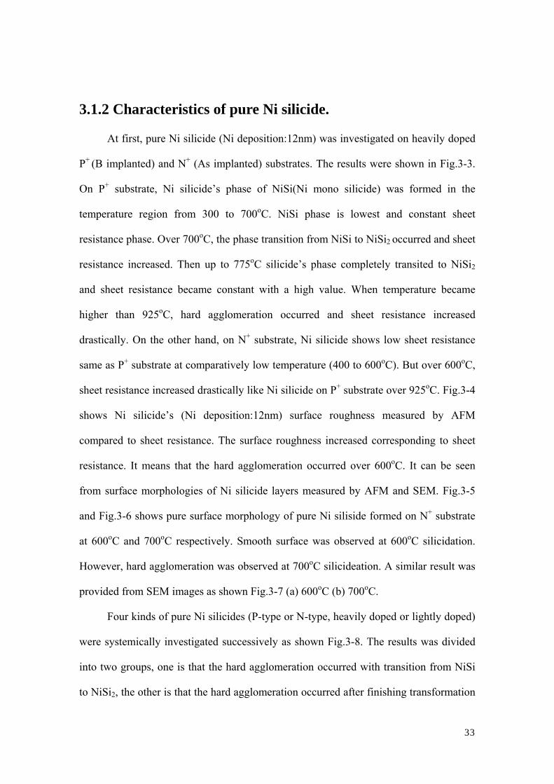
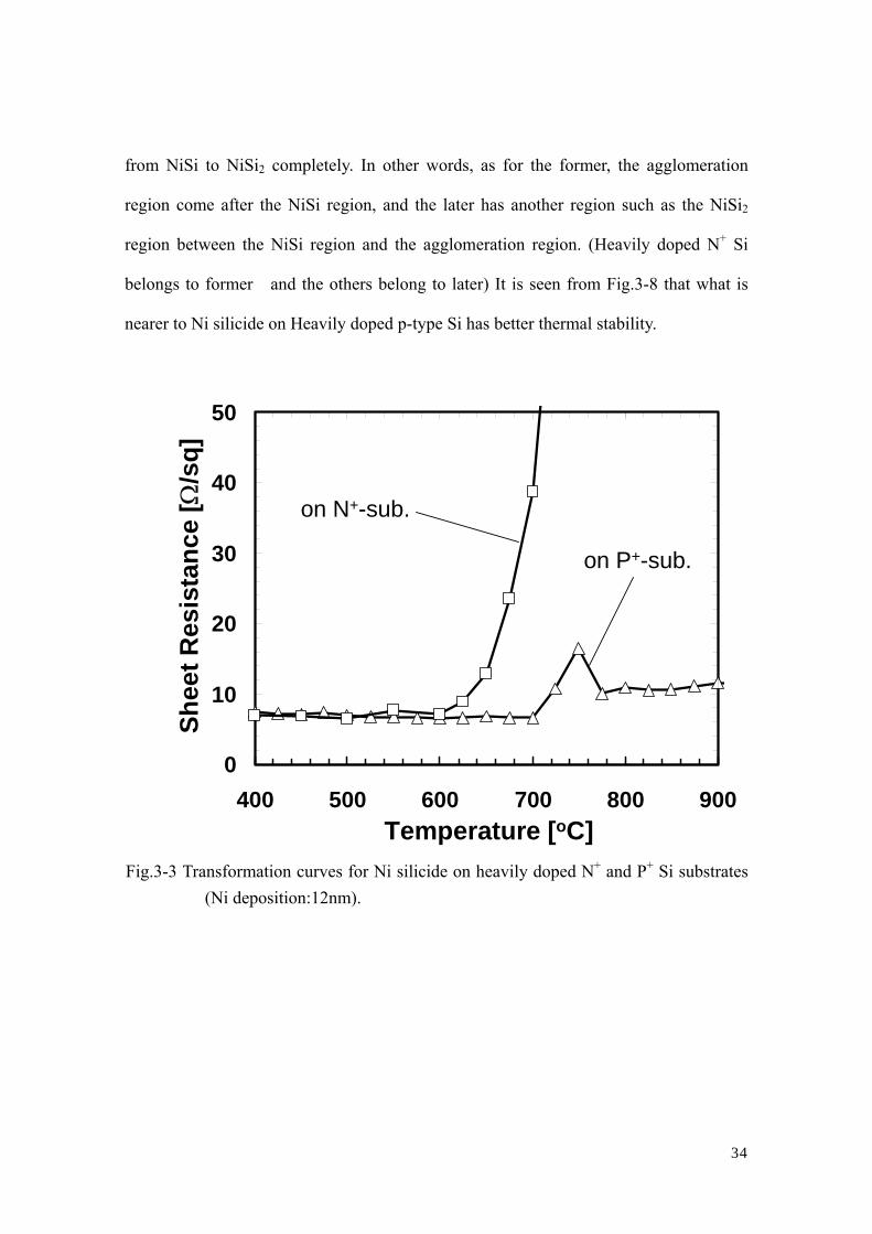
3.1.2 Characteristics of pure Ni silicide.
At first, pure Ni silicide (Ni deposition:12nm) was investigated on heavily doped
P+ (B implanted) and N+ (As implanted) substrates. The results were shown in Fig.3-3.
On P+ substrate, Ni silicide’s phase of NiSi(Ni mono silicide) was formed in the
temperature region from 300 to 700oC. NiSi phase is lowest and constant sheet
resistance phase. Over 700oC, the phase transition from NiSi to NiSi2 occurred and sheet
resistance increased. Then up to 775oC silicide’s phase completely transited to NiSi2
and sheet resistance became constant with a high value. When temperature became
higher than 925oC, hard agglomeration occurred and sheet resistance increased
drastically. On the other hand, on N+ substrate, Ni silicide shows low sheet resistance
same as P+ substrate at comparatively low temperature (400 to 600oC). But over 600oC,
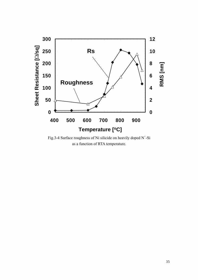
sheet resistance increased drastically like Ni silicide on P+ substrate over 925oC. Fig.3-4
shows Ni silicide’s (Ni deposition:12nm) surface roughness measured by AFM
compared to sheet resistance. The surface roughness increased corresponding to sheet
resistance. It means that the hard agglomeration occurred over 600oC. It can be seen
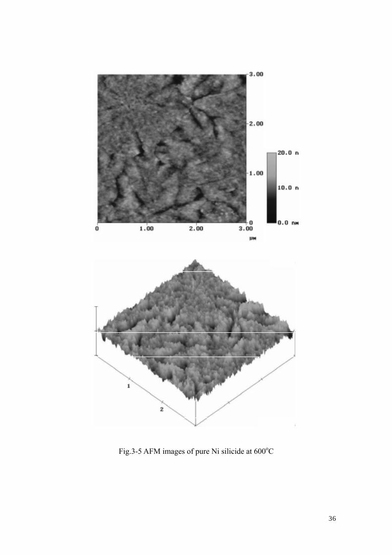
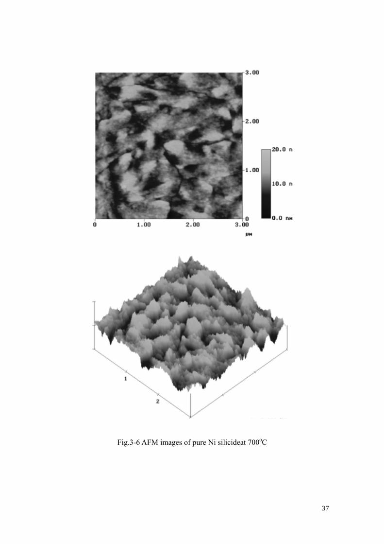
from surface morphologies of Ni silicide layers measured by AFM and SEM. Fig.3-5
and Fig.3-6 shows pure surface morphology of pure Ni siliside formed on N+ substrate
at 600oC and 700oC respectively. Smooth surface was observed at 600oC silicidation.
However, hard agglomeration was observed at 700oC silicideation. A similar result was
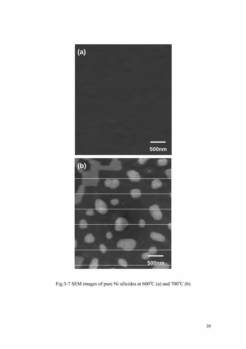
provided from SEM images as shown Fig.3-7 (a) 600oC (b) 700oC.
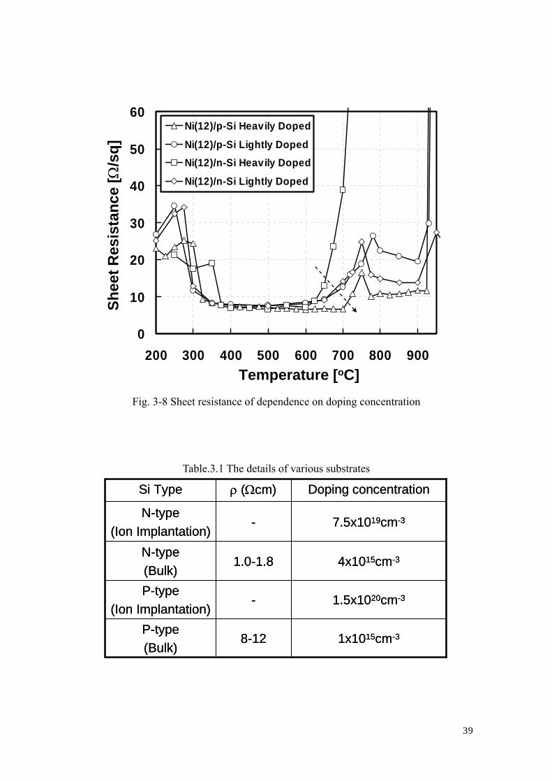
Four kinds of pure Ni silicides (P-type or N-type, heavily doped or lightly doped)
were systemically investigated successively as shown Fig.3-8. The results was divided
into two groups, one is that the hard agglomeration occurred with transition from NiSi
to NiSi2, the other is that the hard agglomeration occurred after finishing transformation
34
from NiSi to NiSi2 completely. In other words, as for the former, the agglomeration
region come after the NiSi region, and the later has another region such as the NiSi2
region between the NiSi region and the agglomeration region. (Heavily doped N+ Si
belongs to former and the others belong to later) It is seen from Fig.3-8 that what is
nearer to Ni silicide on Heavily doped p-type Si has better thermal stability.
0
10
20
30
40
50
400 500 600 700 800 900
on P+-sub.
Temperature [oC]
Shee
t Res
ista
nce
[Ω/s
q]
on N+-sub.
Fig.3-3 Transformation curves for Ni silicide on heavily doped N+ and P+ Si substrates (Ni deposition:12nm).
35
0
50
100
150
200
250
300
400 500 600 700 800 9000
2
4
6
8
10
12
Rs
Roughness
Temperature [oC]
Shee
t Res
ista
nce
[Ω/s
q]
RM
S [n
m]
Fig.3-4 Surface roughness of Ni silicide on heavily doped N+-Si
as a function of RTA temperature.
36
Fig.3-5 AFM images of pure Ni silicide at 600oC
37
Fig.3-6 AFM images of pure Ni silicideat 700oC
38
500nm
500nm
(a)
(b)
Fig.3-7 SEM images of pure Ni silicides at 600oC (a) and 700oC (b)
39
0
10
20
30
40
50
60
200 300 400 500 600 700 800 900
Ni(12)/p-Si Heavily Doped
Ni(12)/p-Si Lightly DopedNi(12)/n-Si Heavily Doped
Ni(12)/n-Si Lightly Doped
Temperature [oC]
Shee
t Res
ista
nce
[Ω/s
q]
Fig. 3-8 Sheet resistance of dependence on doping concentration
Table.3.1 The details of various substrates
1.5x1020cm-3-P-type
(Ion Implantation)
4x1015cm-31.0-1.8N-type(Bulk)
7.5x1019cm-3-N-type
(Ion Implantation)
Doping concentrationρ (Ωcm)Si Type
1x1015cm-38-12P-type(Bulk)
1.5x1020cm-3-P-type
(Ion Implantation)
4x1015cm-31.0-1.8N-type(Bulk)
7.5x1019cm-3-N-type
(Ion Implantation)
Doping concentrationρ (Ωcm)Si Type
1x1015cm-38-12P-type(Bulk)
40
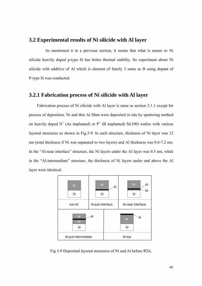
3.2 Experimental results of Ni silicide with Al layer
As mentioned it in a previous section, it seems that what is nearer to Ni
silicide heavily doped p-type Si has better thermal stability. So experiment about Ni
silicide with additive of Al which is element of family 3 same as B using dopant of
P-type Si was conducted.
3.2.1 Fabrication process of Ni silicide with Al layer
Fabrication process of Ni silicide with Al layer is same as section 3.1.1 except for
process of deposition. Ni and thin Al films were deposited in situ by sputtering method
on heavily doped N+ (As implanted) or P+ (B implanted) Si(100) wafers with various
layered structures as shown in Fig.3-9. In each structure, thickness of Ni layer was 12
nm (total thickness if Ni was separated to two layers) and Al thickness was 0.6-7.2 nm.
In the “Al-near interface” structure, the Ni layers under the Al layer was 0.5 nm, while
in the “Al-intermediate” structure, the thickness of Ni layers under and above the Al
layer were identical.
Si
Si
Si
SiSi
Ni Ni
non-Al Al-just interface Al-near interface
Al-just intermediate Al-top
NiNiNi
Ni
Al
Al
Al
Al
Ni
Fig 3-9 Deposited layered structures of Ni and Al before RTA.
41
3.2.2 Characteristics of Ni silicide with Al layer
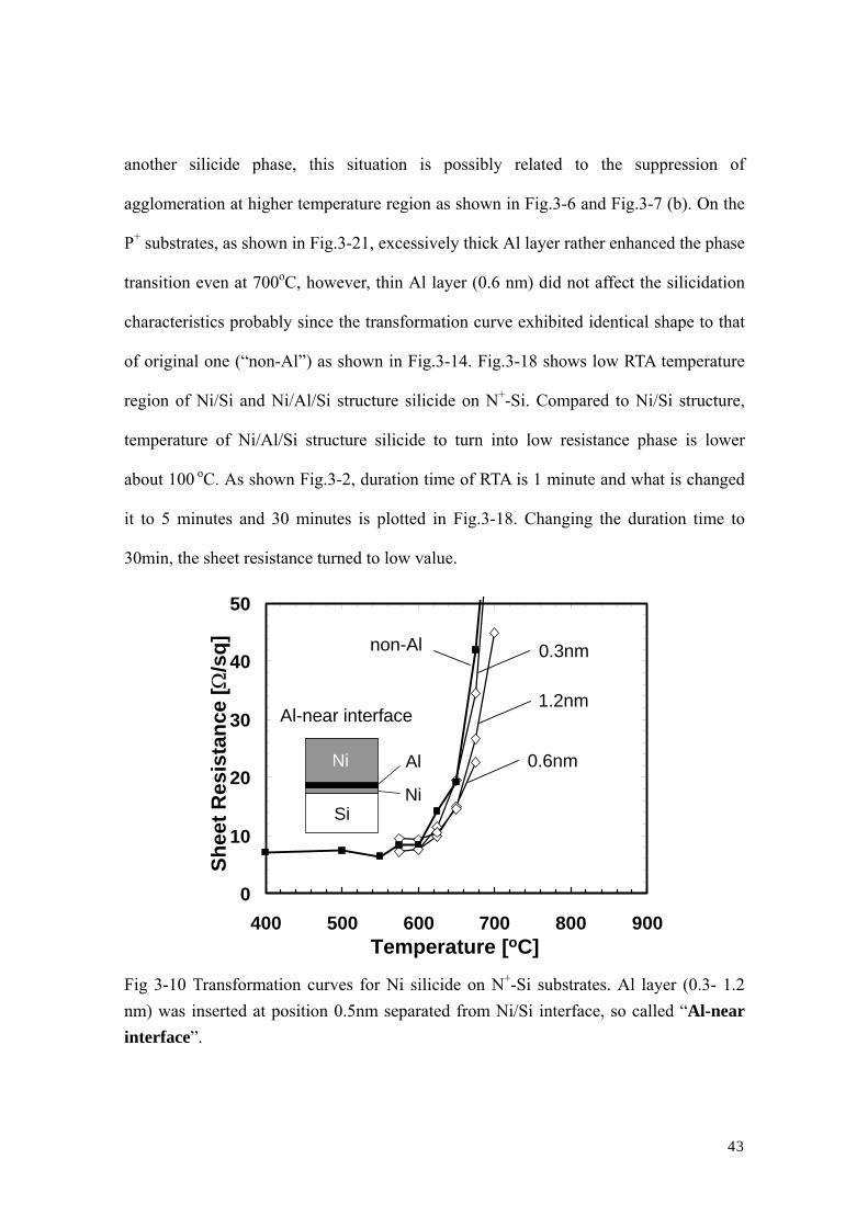
In order to overcome the problem of the poor thermal stability on the N+ substrates,
various layered structures as shown in Fig.9 were examined. The transformation curves
for the “Al-top”, “Al-intermediate” and “Al-near interface” structure with various Al
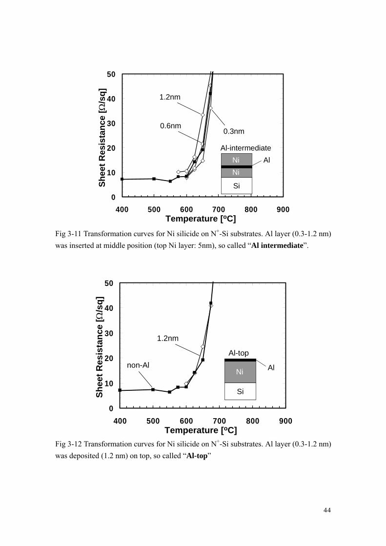
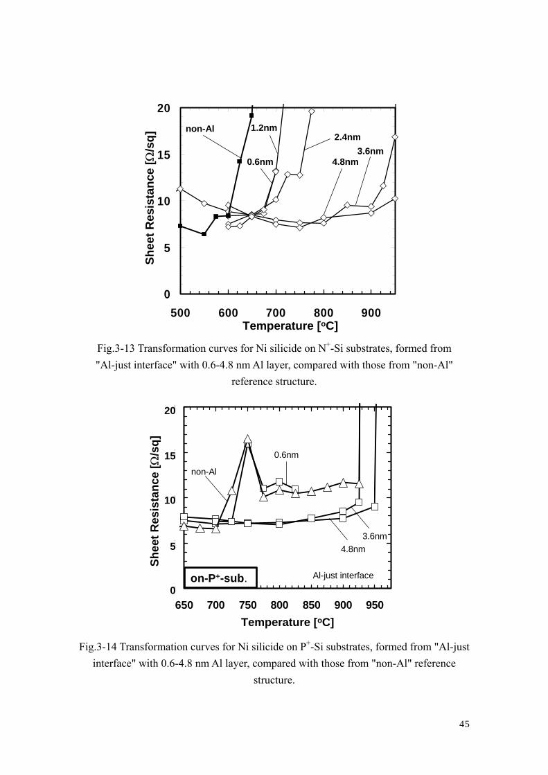
thicknesses on the N+ substrates are shown in Fig.3-10, Fig.3-11, and Fig.3-12
respectively. The obtained curves for these structures were all close to the reference
curve of the “non-Al” structure, indicating no apparent improvement on thermal
stability. On the other hand, only the case of “Al-just interface” exhibited obvious
improvement of thermal stability on N+ substrates as shown in Fig.13, in which
relatively low sheet resistance was maintained up to 900oC with increasing thickness of
the inserted Al layer. Transformation curves for the case of the “Al-just interface” were
observed also on the P+ substrates as shown in Fig.14. The sheet resistances for the case
of the “Al-just interface” were low up to higher temperature comparing to the case of
“non-Al” structure. In the case of 0.6 nm Al addition, the transformation curve was
identical to that of “non-Al”, however, the curves became flat for the case of thicker Al
addition (3.6 nm and 4.8 nm).
In the case of the “non-Al”, significant agglomeration was observed(mentioned it
in section 3.1.1), which resulted in the very high sheet resistance. On the other hand, in
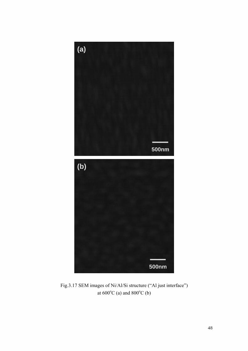
the case of “Al-just interface”, the surfaces were very smooth even at as high as 800oC
by surface morphology observed by AFM and SEM shown in Fig.3-15, Fig.3-16, and
Fig.3-17. The uniform silicide layers obtained in the wide temperature range is
considered to provide rather flat characteristics in the transformation curves as shown in
Fig.3-13.
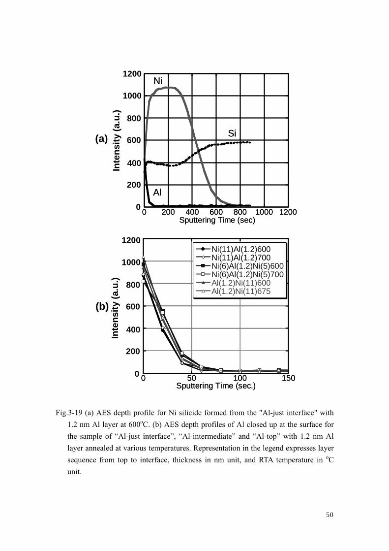
Behavior of the deposited Al was investigated through observation of AES depth
42
profiles after these silicidation processes. It was fond that almost all Al segregated at the
surface after the RTA even if the Al had been deposited under the Ni in the initial stage
(“Al-just interface”) as shown in Fig.3-19 (a). Furthermore, the Al segregation was
observed independent of the initial layered structures of deposition as shown in Fig.3-19
(b), in which Al profiles at the surface are magnified for the cases of 1.2 nm Al
deposition in the “Al-just interface”, “Al-intermediate” and “Al-top” structures after
RTA over 600oC. This means that Ni and Al diffused each other but most of Al was not
taken into the formed silicide layers. It should be noticed that the only 0.5 nm separation
of Al from the interface, i.e., the “Al-near interface” structure (Fig.9), degraded the
effect of thermal stability improvement. It indicates that existence of Al between Ni and
Si in the initial stage of silicidation process is essential and Al involvement in the later
stage is not so significant.
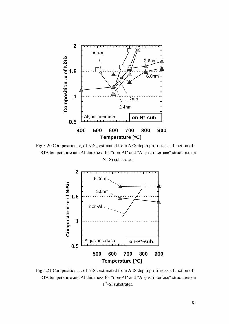
Structure of the Ni silicide layers were estimated from the AES depth profiles. The
averaged composition x of NiSix was evaluated from the relative intensity ratio of Ni
and Si in the silicide layer (Fig.3-19 (a)) for each sample. The obtained evaluated
compositions were plotted as a function of RTA temperature for the “non-Al” and the
“Al-just interface” samples as shown in Fig.3-20 and Fig.3-21. On the N+ substrates, as
shown in Fig.3-20, increase in x with RTA temperature was found to be reduced as
thickness of Al increased. The value of x (1<x<2) is considered to represent mixture
ratio of NiSi(x=1) and NiSi2(x=2). Phase transition from NiSi to NiSi2 occurred entirely
for the “non-Al” and the “Al-just interface” with thiner Al (<2.4 nm) in the temperature
region of 600-750oC. However, in the case of the “Al-just interface” with thicker Al
(>2.4 nm), the increase in x seemed to saturate between 1 and 2. Although it is not clear
whether this means coexistence of NiSi domain and NiSi2 domain or formation of
43
another silicide phase, this situation is possibly related to the suppression of
agglomeration at higher temperature region as shown in Fig.3-6 and Fig.3-7 (b). On the
P+ substrates, as shown in Fig.3-21, excessively thick Al layer rather enhanced the phase
transition even at 700oC, however, thin Al layer (0.6 nm) did not affect the silicidation
characteristics probably since the transformation curve exhibited identical shape to that
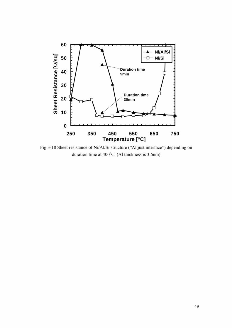
of original one (“non-Al”) as shown in Fig.3-14. Fig.3-18 shows low RTA temperature
region of Ni/Si and Ni/Al/Si structure silicide on N+-Si. Compared to Ni/Si structure,
temperature of Ni/Al/Si structure silicide to turn into low resistance phase is lower
about 100 oC. As shown Fig.3-2, duration time of RTA is 1 minute and what is changed
it to 5 minutes and 30 minutes is plotted in Fig.3-18. Changing the duration time to
30min, the sheet resistance turned to low value.
0
10
20
30
40
50
400 500 600 700 800 900
1.2nm
0.6nm
0.3nmnon-Al
Temperature [oC]
Shee
t Res
ista
nce
[Ω/s
q]
Si
Ni Al
Ni
Al-near interface
Fig 3-10 Transformation curves for Ni silicide on N+-Si substrates. Al layer (0.3- 1.2 nm) was inserted at position 0.5nm separated from Ni/Si interface, so called “Al-near interface”.
44
0
10
20
30
40
50
400 500 600 700 800 900Temperature [oC]
Shee
t Res
ista
nce
[Ω/s
q] 1.2nm
0.6nm0.3nm
Si
NiNi
AlAl-intermediate
Fig 3-11 Transformation curves for Ni silicide on N+-Si substrates. Al layer (0.3-1.2 nm) was inserted at middle position (top Ni layer: 5nm), so called “Al intermediate”.
0
10
20
30
40
50
400 500 600 700 800 900Temperature [oC]
Shee
t Res
ista
nce
[Ω/s
q]
1.2nm
non-Al
Si
Ni Al
Al-top
Fig 3-12 Transformation curves for Ni silicide on N+-Si substrates. Al layer (0.3-1.2 nm) was deposited (1.2 nm) on top, so called “Al-top”
45
0
5
10
15
20
500 600 700 800 900Temperature [oC]
Shee
t Res
ista
nce
[Ω/s
q]
non-Al
0.6nm
1.2nm2.4nm
3.6nm4.8nm
Fig.3-13 Transformation curves for Ni silicide on N+-Si substrates, formed from "Al-just interface" with 0.6-4.8 nm Al layer, compared with those from "non-Al"
reference structure.
Fig.3-14 Transformation curves for Ni silicide on P+-Si substrates, formed from "Al-just interface" with 0.6-4.8 nm Al layer, compared with those from "non-Al" reference
structure.
0
5
0
5
0
650 700 750 800 850 900 950
Si
Ni Al
Al-just interfaceon-P+-sub.
non-Al
3.6nm4.8nm
0.6nm
650Temperature [oC]
Shee
t Res
ista
nce
[Ω/s
q]
20
15
10
5
0
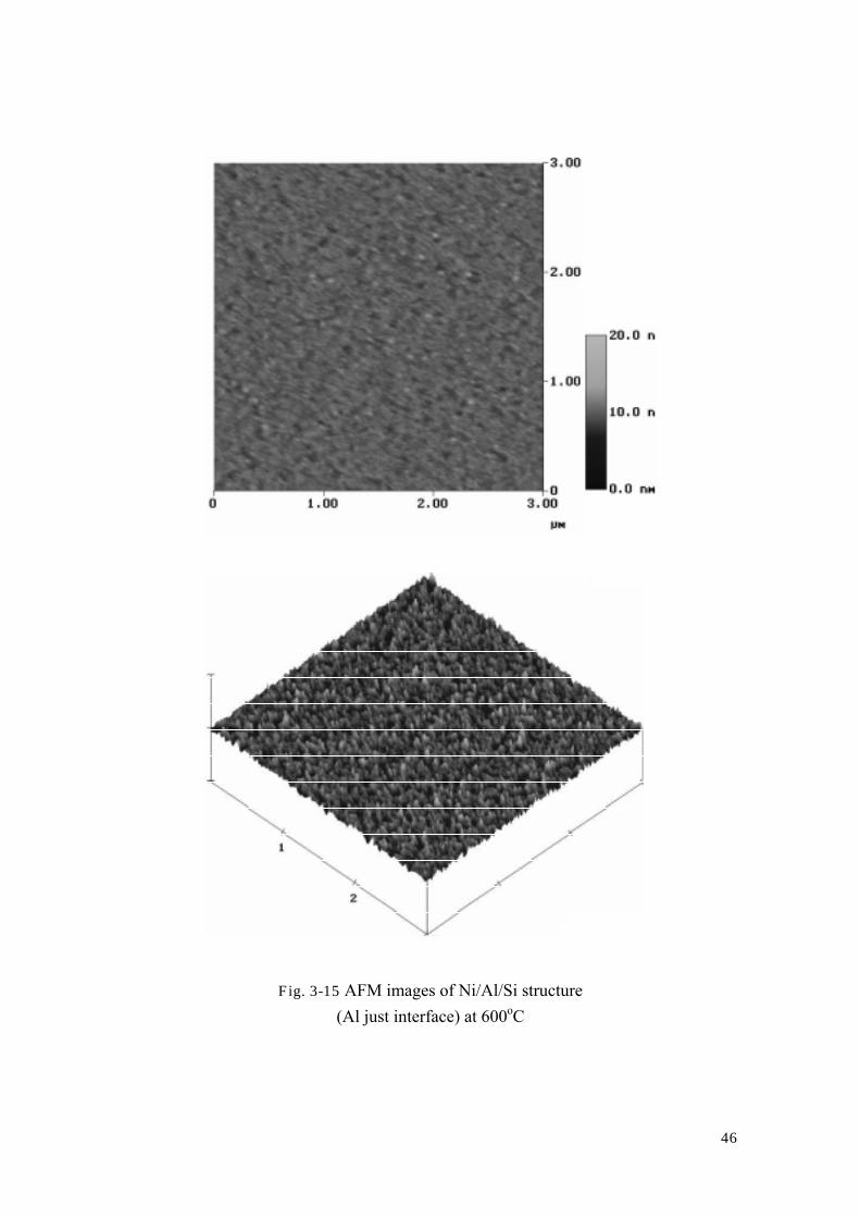
46
Fig. 3-15 AFM images of Ni/Al/Si structure
(Al just interface) at 600oC
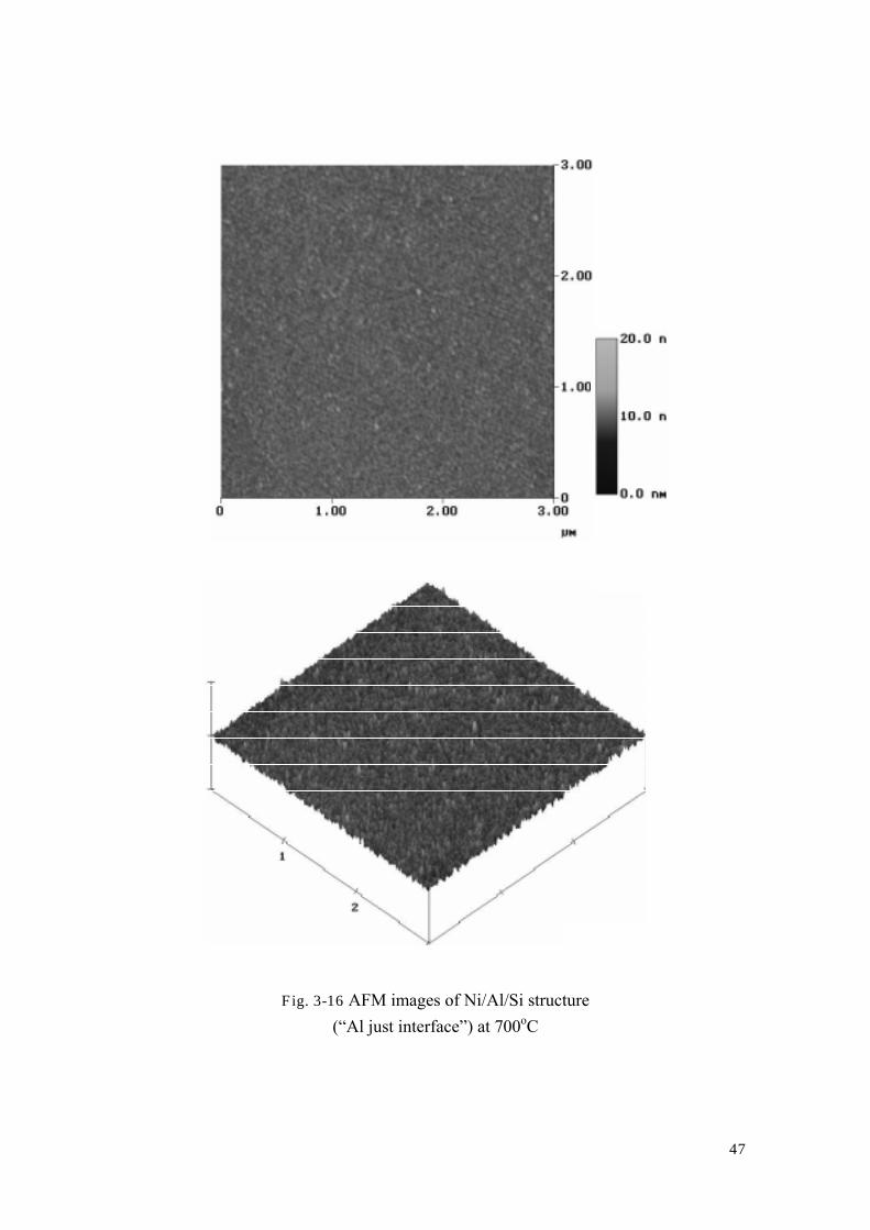
47
Fig. 3-16 AFM images of Ni/Al/Si structure
(“Al just interface”) at 700oC
48
500nm
500nm
(a)
(b)
Fig.3.17 SEM images of Ni/Al/Si structure (“Al just interface”) at 600oC (a) and 800oC (b)
49
0
10
20
30
40
50
60
250 350 450 550 650 750
Duration time 5min
Duration time 30min
Ni/Al/SiNi/Si
Temperature [oC]
Shee
t Res
ista
nce
[Ω/s
q]
Fig.3-18 Sheet resistance of Ni/Al/Si structure (“Al just interface”) depending on
duration time at 400oC. (Al thickness is 3.6nm)
50
0 50 100 150
Ni(11)Al(1.2)600Ni(11)Al(1.2)700Ni(6)Al(1.2)Ni(5)600Ni(6)Al(1.2)Ni(5)700Al(1.2)Ni(11)600Al(1.2)Ni(11)675
Sputtering Time (sec.)0 50 100 150
Ni(11)Al(1.2)600Ni(11)Al(1.2)700Ni(6)Al(1.2)Ni(5)600Ni(6)Al(1.2)Ni(5)700Al(1.2)Ni(11)600Al(1.2)Ni(11)675
Sputtering Time (sec.)
0 200 400 600 800 1000 1200Sputtering Time (sec)
Ni
Si
Al
0 200 400 600 800 1000 1200Sputtering Time (sec)
Ni
Si
Al
1200
1000
800
600
400
200
0
(a)
(b)
Inte
nsity
(a.u
.)
1200
1000
800
600
400
200
Inte
nsity
(a.u
.)
0
Fig.3-19 (a) AES depth profile for Ni silicide formed from the "Al-just interface" with 1.2 nm Al layer at 600oC. (b) AES depth profiles of Al closed up at the surface for the sample of “Al-just interface”, “Al-intermediate” and “Al-top” with 1.2 nm Al layer annealed at various temperatures. Representation in the legend expresses layer sequence from top to interface, thickness in nm unit, and RTA temperature in oC unit.
51
Fig.3.20 Composition, x, of NiSix estimated from AES depth profiles as a function of
RTA temperature and Al thickness for "non-Al" and "Al-just interface" structures on N+-Si substrates.
400 500 600 700 800 900Temperature [oC]
on-P+-sub.
non-Al
6.0nm
3.6nm
Al-just interface0.5
1
1.5
2
Com
posi
tion
:x o
f NiS
ix
Fig.3.21 Composition, x, of NiSix estimated from AES depth profiles as a function of
RTA temperature and Al thickness for "non-Al" and "Al-just interface" structures on P+-Si substrates.
0.5
1
1.5
2
40.5
1
1.5
2
400 500 600 700 800 900Temperature [oC]
Com
posi
tion
:x o
f NiS
ix
on-N+-sub.
1.2nm
2.4nm
3.6nm
6.0nm
non-Al
Al-just interface
52
3.3 Experimental results of Ni silicide with Al interlayer using
TEG wafer
As mentioned in section 1.3, when the line width is pretty narrow, so called
narrow line effect occurs in TiSi2. It is said that the narrow line effect was not observed
about Ni silicide, but the property of Ni silicide may be changed by the addition metal.
Therefore experimental of Ni silicide with Al interlayer using TEG wafer was
conducted.
3.3.1 Fabrication process of Ni silicide with Al layer on TEG
wafer
Fabrication process of Ni silicide with Al layer on TEG wafer shown Fig.3-1.
Cleaning process was as follows. TEG wafers were dipped into UPW first for 5 minuets.
Secondary, they were dipped hydrofluoric acid (HF) for 1 minuets to remove the native
oxide. After that, the wafer was rinsed in UPW and loaded to suppurating system
immediately. Deposition and Annealing process were performed same as previous
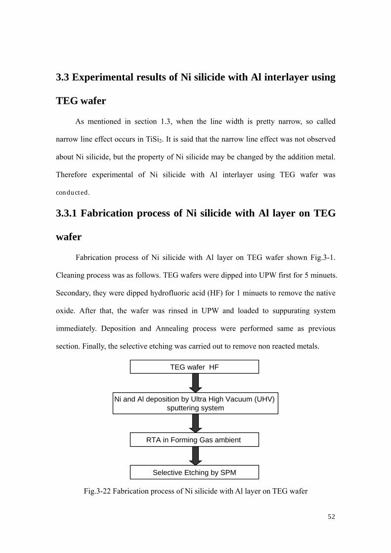
section. Finally, the selective etching was carried out to remove non reacted metals.
TEG wafer HF
Ni and Al deposition by Ultra High Vacuum (UHV) sputtering system
RTA in Forming Gas ambient
Selective Etching by SPM Fig.3-22 Fabrication process of Ni silicide with Al layer on TEG wafer
53
3.3.2 Characteristics of Ni silicide with Al layer on TEG wafer
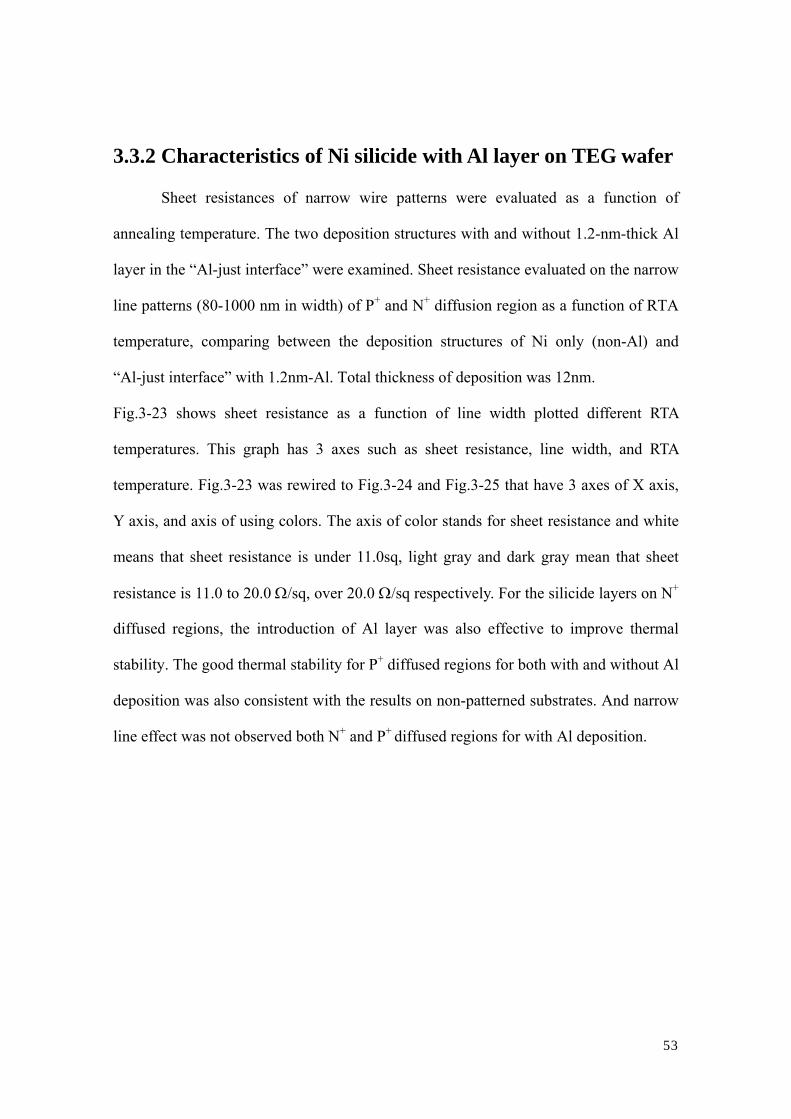
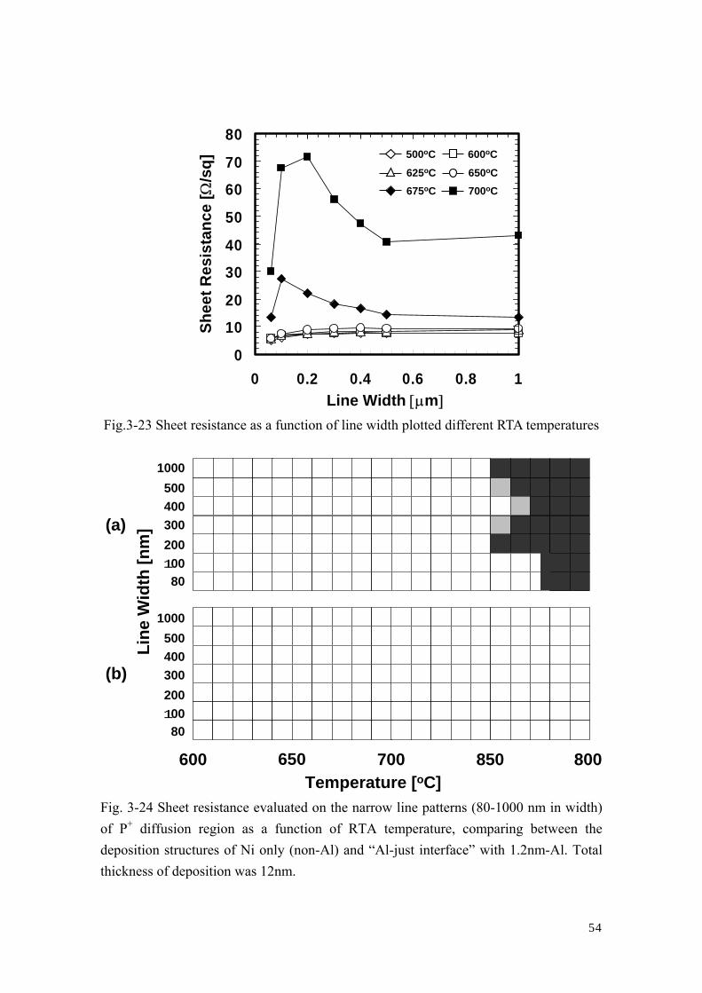
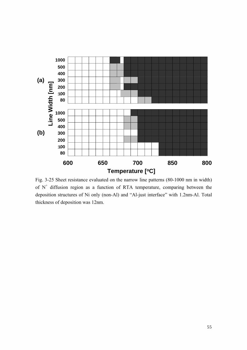
Sheet resistances of narrow wire patterns were evaluated as a function of
annealing temperature. The two deposition structures with and without 1.2-nm-thick Al
layer in the “Al-just interface” were examined. Sheet resistance evaluated on the narrow
line patterns (80-1000 nm in width) of P+ and N+ diffusion region as a function of RTA
temperature, comparing between the deposition structures of Ni only (non-Al) and
“Al-just interface” with 1.2nm-Al. Total thickness of deposition was 12nm.
Fig.3-23 shows sheet resistance as a function of line width plotted different RTA
temperatures. This graph has 3 axes such as sheet resistance, line width, and RTA
temperature. Fig.3-23 was rewired to Fig.3-24 and Fig.3-25 that have 3 axes of X axis,
Y axis, and axis of using colors. The axis of color stands for sheet resistance and white
means that sheet resistance is under 11.0sq, light gray and dark gray mean that sheet
resistance is 11.0 to 20.0 Ω/sq, over 20.0 Ω/sq respectively. For the silicide layers on N+
diffused regions, the introduction of Al layer was also effective to improve thermal
stability. The good thermal stability for P+ diffused regions for both with and without Al
deposition was also consistent with the results on non-patterned substrates. And narrow
line effect was not observed both N+ and P+ diffused regions for with Al deposition.
54
Line Width [µm]
Shee
t Res
ista
nce
[Ω/s
q]
0
10
20
30
40
50
60
70
80
0 0.2 0.4 0.6 0.8 1
500oC
625oC675oC
600oC
650oC700oC
Fig.3-23 Sheet resistance as a function of line width plotted different RTA temperatures
Line
Wid
th [n
m]
1000500400300200100
80
1000500400300200100
80
600 650 700 800850Temperature [oC]
(a)
(b)
Fig. 3-24 Sheet resistance evaluated on the narrow line patterns (80-1000 nm in width) of P+ diffusion region as a function of RTA temperature, comparing between the deposition structures of Ni only (non-Al) and “Al-just interface” with 1.2nm-Al. Total thickness of deposition was 12nm.
55
Line
Wid
th [n
m]
1000500400300200100
80
1000500400300200100
80
600 650 700 800850Temperature [oC]
(a)
(b)
Fig. 3-25 Sheet resistance evaluated on the narrow line patterns (80-1000 nm in width) of N+ diffusion region as a function of RTA temperature, comparing between the deposition structures of Ni only (non-Al) and “Al-just interface” with 1.2nm-Al. Total thickness of deposition was 12nm.
56
3.4 Experimental results of Ni silicide with other metal layers
Experiments about Ni silicide with additive of B, Sn, and Pt was conducted. B is
element of family 3 same as Al, Sn is element of family 4 same as C which was reported
as good element for Ni silicide [6] and Pt was reported a lot for additive metal of Ni
silicide [7-15].
3.4.1 Characteristics of Ni silicide with other metal layers
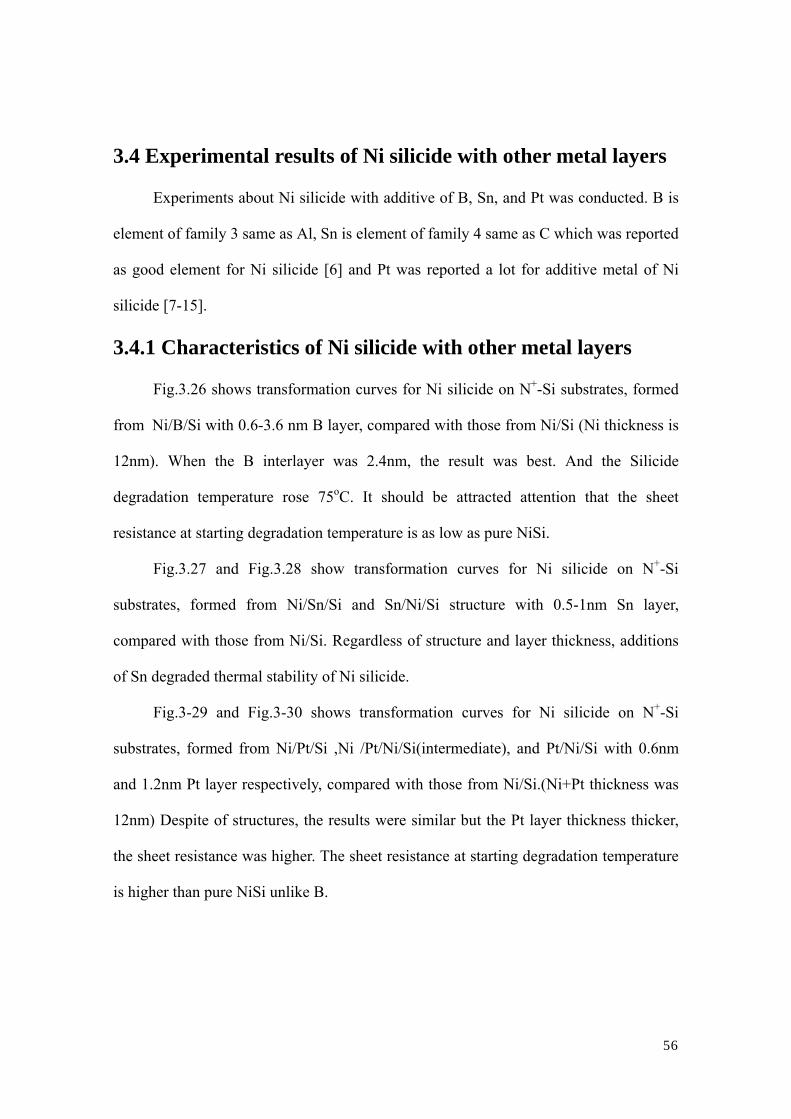
Fig.3.26 shows transformation curves for Ni silicide on N+-Si substrates, formed
from Ni/B/Si with 0.6-3.6 nm B layer, compared with those from Ni/Si (Ni thickness is
12nm). When the B interlayer was 2.4nm, the result was best. And the Silicide
degradation temperature rose 75oC. It should be attracted attention that the sheet
resistance at starting degradation temperature is as low as pure NiSi.
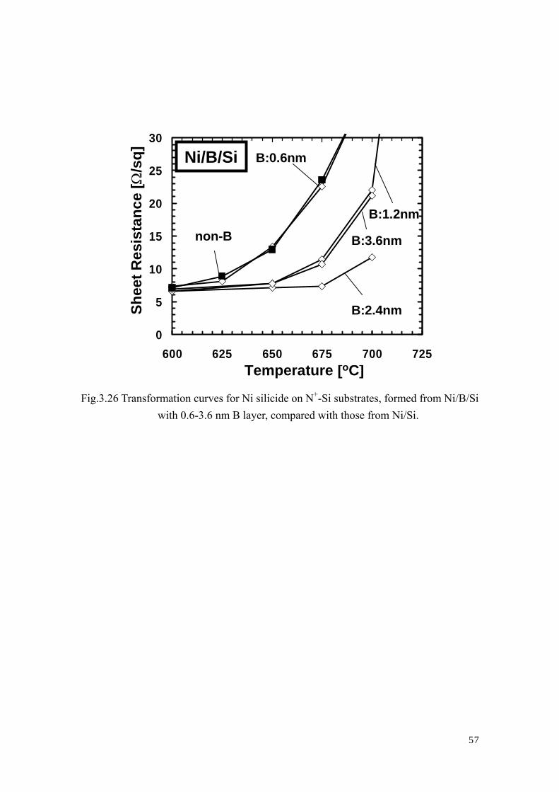
Fig.3.27 and Fig.3.28 show transformation curves for Ni silicide on N+-Si
substrates, formed from Ni/Sn/Si and Sn/Ni/Si structure with 0.5-1nm Sn layer,
compared with those from Ni/Si. Regardless of structure and layer thickness, additions
of Sn degraded thermal stability of Ni silicide.
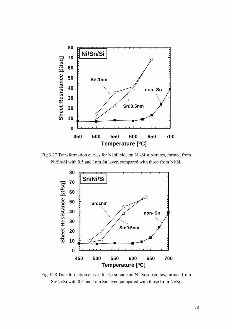
Fig.3-29 and Fig.3-30 shows transformation curves for Ni silicide on N+-Si
substrates, formed from Ni/Pt/Si ,Ni /Pt/Ni/Si(intermediate), and Pt/Ni/Si with 0.6nm
and 1.2nm Pt layer respectively, compared with those from Ni/Si.(Ni+Pt thickness was
12nm) Despite of structures, the results were similar but the Pt layer thickness thicker,
the sheet resistance was higher. The sheet resistance at starting degradation temperature
is higher than pure NiSi unlike B.
57
Temperature [oC]
Shee
t Res
ista
nce
[Ω/s
q]
0
5
10
15
20
25
30
600 625 650 675 700 725
B:2.4nm
B:3.6nm
B:1.2nm
B:0.6nm
non-B
Ni/B/Si
Fig.3.26 Transformation curves for Ni silicide on N+-Si substrates, formed from Ni/B/Si with 0.6-3.6 nm B layer, compared with those from Ni/Si.
58
0
10
20
30
40
50
60
70
80
450 500 550 600 650 700
Ni/Sn/Si
Sn:1nm
Sn:0.5nm
non- Sn
Temperature [oC]
Shee
t Res
ista
nce
[Ω/s
q]
Fig.3.27 Transformation curves for Ni silicide on N+-Si substrates, formed from Ni/Sn/Si with 0.5 and 1nm Sn layer, compared with those from Ni/Si.
0
10
20
30
40
50
60
70
80
450 500 550 600 650 700
Sn/Ni/Si
Sn:1nm
Sn:0.5nm
non- Sn
Temperature [oC]
Shee
t Res
ista
nce
[Ω/s
q]
Fig.3.28 Transformation curves for Ni silicide on N+-Si substrates, formed from
Sn/Ni/Si with 0.5 and 1nm Sn layer, compared with those from Ni/Si.
59
0
5
10
15
20
25
30
550 600 650 700 750 800
Pt:5%
Temperature [oC]
Shee
t Res
ista
nce
[Ω/s
q] Ni/Pt/Ni/SiPt/Ni/Si
Ni/Pt/Si
Ni/Si
Fig.3.29 Transformation curves for Ni silicide on N+-Si substrates, formed from
Ni/Pt/Si ,Ni /Pt//Ni/Si(intermediate), and Pt/Ni/Si with 0.6 nm Pt layer, compared with those from Ni/Si.
0
5
10
15
20
25
30
550 600 650 700 750 800
Pt:10%Ni/Pt/Ni/SiPt/Ni/Si
Ni/Pt/Si
Ni/Si
Temperature [oC]
Shee
t Res
ista
nce
[Ω/s
q]
Fig.3.30 Transformation curves for Ni silicide on N+-Si substrates, formed from
Ni/Pt/Si ,Ni /Pt//Ni/Si(intermediate), and Pt/Ni/Si with 1.2 nm Pt layer, compared with those from Ni/Si.
60
Chapter 4 CONCLUSIONS
61
4.1 Results of This Study
To begin with, we investigated pure Ni silicide on heavily doped N+-Si. From it,
we found the degrading temperature of Ni silicide on heavily doped N+-Si was lower
about 100oC than that of Ni silicide on heavily doped P+-Si and the degrading was
caused by hard agglomeration.
Secondary, we investigated Ni silicide with Al layer to overcome the problem of
the poorer thermal stability on the N+ substrates, and various layered structures as
Al/Ni/Si, Ni/Al/Ni/Si, and Ni/Al/Si were examined. Al/Ni/Si and Ni/Al/Ni/Si structures
were not effective to improve the thermal stability of Ni silicide on the N+ substrates,
but the Ni/Al/Si structure was so effective to improve the thermal stability Ni silicide on
the N+ substrates especially Al thickness was over 2.4nm. Sheet resistance of Ni silicide
with over 2.4nm Al layer inserting Ni-Si interface maintained under 10Ω/sq up to 900oC
which is lower than those of NiSi2 seen on P+ substrate. And very smooth surface
morphologies were observed from SEM and AFM images at 800oC. The same results
were observed on P+ substrate. Composition, x, of NiSix estimated from AES depth
profiles. As far as the Ni/Al/Si structure (Al thickness: < 2.4nm) is concerned, the
increase in x seemed to saturate between 1 and 2. Although it is not clear whether this
means coexistence of NiSi domain and NiSi2 domain or formation of another silicide
phase, this situation is possibly related to the suppression of agglomeration at higher
temperature region. Sheet resistances of narrow wire patterns were evaluated using TEG
wafers. And narrow line effect was not observed both N+ and P+ diffused regions for
with Al (1.2nm) deposition.
Finally, experiments about Ni silicide with additive of B, Sn, and Pt were
conducted. We found the Ni silicide on N+-Si substrates formed from Ni/B/Si with B
62
layer effective. And the Silicide degradation temperature rose 75oC at the maximum. B
is element of family 3 same as Al, therefore we showed possibility that elements of
family 3 such as Al and B is effective materials for Ni silicide.
4.2 Future Issues
We showed possibility that elements of family 3 such as Al and B is effective
materials for Ni silicide. However the mechanism of its effect is not understood
completely. The mechanism should be made clear for applications of silicide for future
device. At the same time, a trial to really use this result for real device should be made.
63
Acknowledgements
I wishes to express his deep gratitude to his supervisor Professor Hiroshi Iwai, who
gave him great guidance and support during his Master study. He led me to a treasure of
knowledge and showed me what a researcher should be. The experience of doing
research in IWAI Lab. was invaluable to me.
I would like to express my sincere appreciation to Associate Professor Kazuo
Tsutsui of his very wonderful advices and warm-hearted instructions in my research. He
always enlightens my confidence when I have difficulty.
I also want to thank Professor Noriaki Nakayama for his warmhearted
encouragement to make progress in my research.
I want to express my gratitude to Visiting Professor Takeo Hattori and Visiting
Professor Nobuyuki Sugii, who always give me good advices about my research.
I also want to thank Assistant Kuniyuki Kakushima and Assistant Parhat Ahmet
for providing an excellent experiment environment and tremendous supports for my
research.
I also wants to thank my other silicide group member, Mr. Koji Nagahiro. I want to
thank them for their helpful discussions and good cooperation in experiment. I need to
thank former silicide group member Xiang Ruifei for providing help in using the
experimental tool. Special thanks go to Technical Officer Dai Syoji for teaching me
how to carry out SEM measurement.
Many thanks to current and former graduate students, Dr. NG Jin Aun, Dr. Atsushi
Kuriyama, Dr. Molina Reyes Joel, Dr. Yuichiro Sasaki, Dr. Hendriansyah Sauddin, Mr.
Jaeyeol Song, Mr. Yasuhiro Shiino, Mr. Masayuki Nakagawa, Mr. Kiichi Tachi ,
64
Manabu Adachi, Yoshihisa Ohisi, Tamasa Kawanago, Soushi Staoh Yasuhiro
Morozumi and Ko-ichi Okamoto for many helpful discussions.
I would very much appreciate the great supports from secretaries, Ms. Mikoto
Karakawa, Ms. Yuki Hashizume, Ms. Akiko Matsumoto, Ms. Takako Fukuyama, and
Ms. Nobuko Iizuka.
This study was supported by ULSI Process Technology Development Center,
Semiconductor Company, Matsushita Electric Industrial Co., Ltd. I would like to thank
Dr. Yasutoshi Okuno, Mr. Michikazu Matsumoto, and Mr. Masafumi Kubota for their
useful advices and indispensable support in Si-substrate supplying and measurements.
Takashi Shiozawa
Yokohama, Japan
January, 2007
65
References
[1] International Technology Roadmap for Semiconductors (ITRS) 2006 update.
[2] Yuan Taur and Tak H. Ning, “Fundamentals of MODERN VLSI DEVICES”
CAMBRIDGE UNIVERSITY PRESS.
[3] H. Iwai, T. Ohguro, and H. Ohmi, “NiSi salicide technology for scaled CMOS”
Microelectronic Engineering 60, pp.157-169.
[4] Shi-Li Zhang , Mikael Ostling,Critical Reviews in Solid State and Materials
Sciences, 28(1):1–129 (2003)
[5] Q. Z. Hong, S. Q. Hong, F. M. d’Heurle, and J. M. E. Harper, “Thermal stability of
silicide on polycrystalline Si” Thin Solid Films 253, 479 (1994).
[6] O. Nakatsuka, K. Okubo, A. Sakai, M. Ogawa, Y. Yasuda and S. Zaima,
“Improvement in NiSi/Si contact properties with C-implantaition” Microelectronic
Engineering 82, pp.479-484 (2005)
[7] J. F. Liu, H. B. Chen, J. Y. Feng and J. Zhu, “Improvement of the thermal stability
of NiSi films by using a thin Pt interlayer” Appl. Phys. Lette., 77(14),
pp.2177-2179 (2000).
[8] J. F. Liu, J. Y. Feng and J. Zhu, “Comparison of the thermal stability of NiSi films
in Ni/Pt/(111)Si and Ni/Pt/(100)Si systems” J. Appl. Phys., 90(2) pp.745-749
(2001)
[9] L. W. Cheng, S. L. Cheng, L. J. Chien, H. C. Chien, H. L. Lee, and F. M. Pan,
“Formation of Ni Silicides on (001)Si with a thin interposing Pt layer” J. Vac. Sci.
Technol. A, 18(4), pp.1176-1179(2000).
66
[10] J. Y. Dai, D. Mangelinck, and S.K. Lahiri, Coexistence of hexagonal and
orthorhombic structures in NiSi films containing Pt, Appl. Phys. Lette., Vol.75,
No.15, 1999, pp.2214-2216.
[11] R.N. Wang, Y. He, J. Y. Feng, Explanation of the enhancement of NiSi thermal
stability according to TFD equations and Miedema’s model, Nuclear Instruments
and Methods in Physics Research, Vol.222, Issues 3-4, 2004 pp.462-468.
[12] P. S. Lee, K. L. Pey, D. Mangelinck, J. Ding, D. Z. Chi, J. Y. Dai, and L.Chane,
Phase and Layer Stability of Ni-and Ni(Pt)-Silicides on Narrow Poly-Si Lines,
Journal of The Electrochemical Society, 149(6)G331-G335(2002).
[13] P. S. Lee, K. L. Pey, D, Mangelinck, J. Ding, T. Osipowics, and A. See, Layer
Inversion of Ni(Pt)Si on Mixed Phase Si Films, Electrochemical and Solid-State
Letters, 5(3)G15-G17(2002).
[14] J. F. Liu, J. Y. Feng, and J. Zhu, Film thickness dependence of the NiSi-to-NiSi2
transition temperature in the Ni/Pt/Si(100) system, APPLIED PHYSICS LETTERS
Vol.80, No.2,2002,pp.270-272.
[15] C. Detavernier and C. Lavoie, Influence of Pt addition on the texture of NiSi on
Si(001), APPLIED PHYSICS LETTERS, Vol.18, 2004pp.3549-3551.