high dielectric constant pvdf based …ncl.csircentral.net/1511/1/final_thesis_printed.pdfdoctor of...
TRANSCRIPT

HIGH DIELECTRIC CONSTANT
PVDF BASED NANOCOMPOSITES FOR
APPLICATIONS IN LOW THERMAL
EMISSIVITY AND FIELD EFFECT DEVICES
A THESIS SUBMITTED TO THE
UNIVERSITY OF PUNE
FOR THE DEGREE OF
DOCTOR OF PHILOSOPHY(Ph.D.) IN
PHYSICS BY
CHETAN V. CHANMAL
DR. (MRS.) JYOTI JOG (RESEARCH GUIDE)
POLYMER SCIENCE AND ENGINEERING DIVISION
CSIR-NATIONAL CHEMICAL LABORATORY
PUNE - 411008 (INDIA)
July 2014

CERTIFICATE
This is to Certify that the work presented in the thesis entitled “HIGH
DIELECTRIC CONSTANT PVDF BASED NANOCOMPOSITES FOR
APPLICATIONS IN LOW THERMAL EMISSIVITY AND FIELD EFFECT
DEVICES” by Mr. Chetan V. Chanmal, submitted for the degree Doctor of
Philosophy in Physics was carried out under my supervision at the Polymer Science
and Engineering Division, National Chemical Laboratory, Pune, 411008, India. Such
material as has been obtained from other sources has been duly acknowledged in the
thesis.
Dr. (Mrs.) Jyoti P. Jog
(Research Guide)
Date:
Place: NCL, Pune
DECLARATION
I hereby declare that the work presented in the thesis entitled “HIGH DIELECTRIC
CONSTANT PVDF BASED NANOCOMPOSITES FOR APPLICATIONS IN
LOW THERMAL EMISSIVITY AND FIELD EFFECT DEVICES”, submitted
for Ph. D. Degree in Physics to the University of Pune, has been carried out under the
supervision of Dr. (Mrs.) Jyoti P. Jog at the Polymer Science and Engineering
Division, National Chemical Laboratory, Pune. The work is original and has not been
submitted in part or in full by me for any degree or diploma to this or any other
University.
Chetan V. Chanmal
(Research Students)
Date:
Place: NCL, Pune


Acknowledgements
During the course of my thesis work there were many people who were instrumental
in helping me. I would like to thank all those people who made this thesis possible and
an enjoyable experience for me.
My foremost thanks go to my research advisor Dr. Jyoti P. Jog for her support,
guidance, encouragement and for allowing me freedom to pursue my interests and
learn how to learn. Under her guidance I not only learned how to conduct research,
but also how to communicate my ideas. I have learned a great deal from interacting
with her.
I take this opportunity with deep sense of gratitude to record my sincere thanks to Dr.
S. B. Ogale for his keen interest, valuable guidance during this work. His passion
towards research, never lasting enthusiasm, and pursuit for high impact research has
made deep impression on me.
I express my sincere thanks to Dr. S. Sivaram, former Director of National Chemical
Laboratory (CSIR-NCL), Dr. Sourav Pal, Director, National Chemical Laboratory
(CSIR-NCL) for giving me the opportunity to work in this prestigious research
institute. I would like to thank Dr. M. G. Kulkarni, former Head, PSE Division and
Dr. A. J. Verma, Head, PSE Division for their cooperation during the work of thesis. I
would also like to thank the technical and non-technical staff of the Polymer Science
and Engineering division for their help. Many thanks are also due to the staff
members of Students Academic Office for their time-to-time help.
I greatly acknowledge the financial assistance from Council of Scientific and
Industrial Research (CSIR) for providing a research fellowship for carrying out the
doctoral work. I would also like to thank DRDO, Jodhpur for providing financial
support.
I take this opportunity to thank Dr.S.I.Patil, Head, Department of Physics, University
of Pune for his help in admission process. A special thanks to Prof. S.V. Bhoraskar
and Dr. V.L.Mathe for their encouragement and fruitful scientific discussion. Thanks
are due to Dr. N. B. Chaure for his help in FET studies.

I am very much thankful to Mr. Vivek Borkar whose help during this course was
invaluable. I am thankful to all the staff members of NCL especially, Mr. A. B.
Gaikwad (SEM facility), Mrs. Dhoble, Sunita Tombhare, Dr.S.D.Deshpande, and
Dr. Harshavardhan Pol. My sincere thanks to Deenanath Bharati for his help.
My heartfelt thanks go to Prashant Patil and M. dhanalaxmi for your friendship and
support in all ups and downs during this work. Without your help this work would not
be possible. It was a memorable experience and I really enjoyed the time spent
together.
I would also like to thank all lab members of JPJ group: Dr. Santosh Wanjale,
Dr. Rajendra Kalgaonkar, Dr. Harshada Nagar, Dr. L. Priya, Amol Ridhore, Sachin
Punde, Sachin, Usman, MSc. Project students Asha, and Remya for providing The
wonderful working environment.
I had wonderful time to work with the members of SBO group, both past and present:
Dr. Abhimanyu Rana, Dr. Prasad Yadav, Dr. Meenal Deo, Dr. Lily Mandal, Vishal,
Deepti, Rounak, Dr. Parvez, Aniruddha, Anil, and Satish for their help during the
work of the thesis.
I take this opportunity to thank Dr.S.K.Vadagbalkar, Principle, D.B.F. Dayanand
College, Solapur, and Dr. R. N. Mulik, Head, Department of Physics, Dayanand
College, Solapur for their whole-hearted help and constant support from the very first
day in the college. Many thanks are due to teaching staff members of Physics
department Dayanand College, Solapur: Prof. E.K.Kore, Prof. S.D. Chavan, and
Dr.S.G.Pawar. Thanks are also due to the non-teaching staff members of Physics
department.
I am grateful to the Jindam family for their support and encouragement during the
work of the thesis.
I don’t have words to express my feelings towards my parents, their support and
blessings have made me what I am today. Their patience and sacrifice will remain my
inspiration throughout my life. The greatest thanks are to my wife, Nileema for being
with me in all ups and down in this journey.
Chetan Chanmal

List of Nomenclature
PVDF Poly (vinylidene) Fluoride
BaTiO3 Barium titanate
MWCNT Multiwalled Carbon Nanotube
XRD X-ray Diffraction
DRS Dielectric Relaxation Spectroscopy
SEM Scanning Electron Microscopy
TEM Transmission Electron Microscopy
DMA Dynamic Mechanical Analysis
DSC Differential Scanning Calorimetry
PLD Pulsed Laser Deposition
IR Infrared
ATR Attenuated Total Internal Reflection
ITO Indium Tin Oxide
I-V Current Voltage
PVP Poly (4-vinylphenol)
rpm Revolution per minute
List of symbols
f - frequency
fmax - frequency maximum in loss spectra
ω - angular frequency
ε - dielectric permittivity
ε' - real Part of complex dielectric permittivity
ε″ - imaginary part of complex dielectric permittivity
tan δ - dielectric loss tangent
M′ - real part of electric modulus spectra
M″ - imaginary part of electric modulus spectra
σdc - dc conductivity
Δε - dielectric relaxation strength
α, β - shape parameters describing the symmetric and asymmetric broadening of relaxation, respectively.
Ea - activation energy
τ - relaxation time
T - temperature
Tc - Curie temperature
MWS - Maxwell-Wagner-Sillars relaxation
Tg - glass transition temperature
αc - crystalline relaxation
αa - co-operative segmental relaxation
μ - mobility
Ion/off - on off current ratio
VDS - drain source voltage
VGS - gate source voltage

ABSTRACT
A study of polymer nanocomposites is an emerging area in polymer science
where the property improvements are obtained by incorporation of nanofillers in the
polymer matrix. There are three types of nanofillers, viz., nanoparticles having three
dimensions in the nano scale, two-dimensional fillers like nano tubes, and nano clays
with single dimension in the nano scale. Earlier, the research in this field was largely
focused on the improvements in the mechanical, thermal and electrical properties of
the polymer materials. Now, with the significant understanding of structure-property
relations in polymer nanocomposites, research is driven to explore the potential
applications of these materials in diverse fields like organic field effect transistors
(OFET), photodetectors, sensors and light emitting diodes. It is in this context that the
work presented in this thesis has been undertaken to investigate properties and
applications of polymer nanocomposites based on Polyvinylidene Fluoride (PVDF)
with three different types on nanofillers viz. Clay having one dimension in nanoscale,
Carbon nanotubes (MWCNTs) having two dimensions in nanoscale and Barium
Titanate (BaTiO3) having three dimensions in the nanoscale. PVDF is chosen as the
polymer matrix, as it is one of the important polymer because of its potential
application as ferroelectric and pyroelectric material. These properties combined with
high elasticity and processing ability provides a variety of technological applications
of this polymer.
The main objective of the thesis was to explore the applications of polymer
nanocomposites as an alternative material in organic field effect transistor devices and
also to understand the effect of nanofiller on the structure and dielectric properties of
PVDF. The polymer nanocomposite materials presented in this study are potentially
useful as gate insulators and active channel layer in organic field-effect transistors.
Chapter 1 gives basic overview of polymer nanocomposites and properties of
materials used in the thesis. This chapter also discusses the various applications of
polymer nanocomposites relevant to the thesis.
Chapter 2 gives a general outline of the fabrication techniques used for polymer
nanocomposites and basic theory of various techniques used for characterization of
polymer nanocomposites.
Chapter 3 describes the effect of BaTiO3 nanoparticles on the dielectric relaxation
behavior of PVDF. Three dielectric relaxation processes were identified in
PVDF/BaTiO3 nanocomposites, viz. crystalline relaxation (αc), glass transition
relaxation (αa) and Maxwell-Wagner-Sillars (MWS) relaxation. Further, the
PVDF/BaTiO3 nanofibers were prepared by electrospinning technique. The
nanofibers show reduction in the thermal emissivity due to non woven porous
morphology of the electrospun fiber.
In Chapter 4, we have discussed the interesting dielectric properties of
PVDF/MWCNT thin film nanocomposites fabricated by Pulsed Laser Deposition
(PLD) technique. The addition of MWCNT shows enhancement in the polar
ferroelectric β phase of PVDF along with significant enhancement in the dielectric
permittivity near the percolation threshold. We have also fabricated the organic field
effect transistor (OFET) with PVDF/MWCNT nanocomposite thin layer as an active
channel layer. The device shows strong field effect modulation in the drain current.
In Chapter 5, we discuss the fabrication organic field effect transistor using
PVDF/Clay nanocomposites as a gate dielectric layer. The device exhibits excellent
transistor performance with p-type of operation. The OFET also exhibits non-volatile
memory and Infrared (heat) sensing applications due to the ferroelectric and
pyroelectric properties of gate dielectric layer.
The Chapter 6 summarizes the work described in this thesis by presenting the salient
features of the work. Possible avenues for future investigations are also outlined.

Table of Contents
Chapter 1: Introduction and Literature Survey 1 - 30
1.1 Introduction ……………………………………………………………... 2
1.2 Polymer Nanocomposites……………………………………………….... 2
1.3 Poly (vinylidene Fluoride) (PVDF) …………………………………....... 4
1.4 Nanomaterials…………………………………………………………….. 8
1.4.1 Clay……………………………………………………….. 9
1.4.2 MWCNT……………………………………………………... 10
1.4.3 BaTiO3……………………………………………………... 11
1.5 PVDF based Nanocomposites…………………………………………… 12
1.6 Applications of Polymer Nanocomposites……………………………… 15
1.6.1 High Dielectric Constant Materials………………………….. 16
1.6.2 Organic Field Effect Transistor (OFET)…………………….. 17
1.6.3 Thermal Emissivity………………………………………….. 21
1.7 Research Objectives……………………………………………………… 23
1.8 Structure of the Thesis…………………………………………………… 24
1.9 References……………………………………………………………….... 25
Chapter 2: Materials and Experimental Techniques 31-56
2.1 Introduction………………………………………………………………. 32
2.2. Materials………………………………………………………………….. 32
2.2.1 PVDF………………………………………………………… 32
2.2.2 Barium Titanate (BaTiO3)…………………………………… 33
2.2.3 Multiwalled Carbon Nanotubes (MWCNT)…………………. 34
2.2.4 Clay………………………………………………………….. 35
2.3 Fabrication of Nanocomposites………………………………………….. 36
2.3.1 Melt Compounding Technique………………………………. 36
2.3.2 Pulsed Laser Deposition (PLD)……………………………… 36
2.3.3 Electrospinning……………………………………………… 38
2.3.4 Spin Coating………………………………………………… 40

2.4 Characterization Techniques…………………………………………...... 41
2.4.1 X-ray Diffraction (XRD)…………………………………….. 41
2.4.2 ATR-FTIR Spectroscopy……………………………………. 43
2.4.3 Raman Spectroscopy……………………………………….... 45
2.4.4 Scanning Electron Microscopy (SEM)……………………… 46
2.4.5 Transmission Electron Microscopy (TEM)…………………. 48
2.4.6 Dielectric Relaxation Spectroscopy (DRS)…………………. 49
2.4.7 Ferroelectric Analysis……………………………………….. 54
2.5 References…………………………………………………………………….. 55
Chapter 3: Dielectric Relaxation and Low Thermal Emissivity Studies of
PVDF/BaTiO3 Nanocomposites 57-85
Section I: Dielectric Relaxation Dynamics in PVDF/BaTiO3 Nanocomposites
3.I.1 Introduction………………………………………………………………. 58
3.I.2 Experimental……………………………………………………………… 59
3.I.2.1 Materials……………………………………………………. 59
3.I.2.2 Fabrication of PVDF/BaTiO3 Nanocomposites……………. 60
3.I.2.3 Nanocomposite Characterization ………………………….. 60
3.I.3 Results and Discussion……………………………………………………. 61
3.I.3.1 Morphology ………………………………………………... 61
3.I.3.2 Structural Analysis ………………………………………… 62
3.I.3.3 Dielectric Relaxation Spectroscopy (DRS) ……………….. 62
3.I.3.4 Electric Modulus Formalism……………………………….. 67
3.I.3.5 Activation Energy..…………… …………………………… 70
3.I.3.6 Cole-Cole Plot……………………………………………… 72
3.I.4 Conclusions……………………………………………………………….. 73
Section II: Electrospun PVDF/BaTiO3 Nanofibers for Low Thermal Emissivity
3.II.1 Introduction……………………………………………………… 74 3.II.2 Experimental……………………………………………………………… 74
3.II.3 Results and Discussion…………………………………………………… 78
3.II.3.1 Morphology ………………………………………………. 78
3.II.3.2 Structural Analysis………………………………………... 79

3.II.3.3 Thermal Emissivity of PVDF/BaTiO3 nanofibers………… 82
3.II.4 Conclusions……………………………………………………………….. 83
3.II.5 References………………………………………………………………… 83
Chapter 4: Strong Electric Field Modulation of Transport in PVDF/MWCNT
Nanocomposite near the Percolation Threshold 86-111
4.1 Introduction……………………………………………………………….. 87
4.2 Experimental……………………………………………………………… 89
4.2.1 Materials……………………………………………………... 89
4.2.2 PLD Processing of PVDF/MWCNT Thin Films……………. 89
4.2.3 Nanocomposite Characterization…………………………….. 90
4.2.3.1 Morphology ……………………………………….. 90
4.2.3.2 Structural Characterization………………………… 90
4.2.3.3 Dielectric Relaxation Spectroscopy………………... 90
4.2.4 Fabrication of PVDF/MWCNT Nanocomposite FET……….. 91
4.3 Results and Discussion……………………………………………………. 92
4.3.1 Morphology …………………………………………............. 92
4.3.2 Structural Analysis…………………………………………… 93
4.3.3 TEM Analysis………………………………………………... 97
4.3.4 Dielectric Relaxation Spectroscopy (DRS)………………….. 98
4.3.5 AC Conductivity measurements …………………………….. 101
4.3.6 I-V Characteristics…………………………………………… 104
4.3.7 Scanning Tunneling Microscopy (STM)…………………….. 105
4.3.8 Field Effect Device using Nanocomposites as Channel Layer. 106
4.4 Conclusions………………………………………………………………... 108
4.5 References…………………………………………………………………. 108
Chapter 5: Nonvolatile Memory and Infrared (IR) Sensor based on PVDF/Clay
Nanocomposites 112-136
Section I: Dielectric Studies of PVDF/Clay Nanocomposites
5.I.1 Introduction………………………………………………………………. 113
5.I.2 Experimental……………………………………………………………... 114
5.I.2.1 Materials and Processing of Nanocomposites……………... 114

5.I.2.2 Nanocomposite Characterization…………………………… 114
5.I.3 Results and Discussion…………………………………………………… 115
5.I.3.1 Structural Analysis………………………………………… 115
5.I.3.2 Dielectric Studies…………………………………………... 116
5.I.4 Conclusions……………………………………………………………….. 124
Section II: PVDF/Clay Nanocomposites as a Gate Dielectric in Organic FET
5.II.1 Introduction………………………………………………………………. 125
5.II.2 Experimental……………………………………………………………… 126
5.II.3 Results and Discussion……………………………………………………. 128
5.II.3.1 Structural Analysis………………………………………… 128
5.II.3.2 Transistor Characteristics of PVDF/Clay-OFET………….. 129
5.II.3.3 Nonvolatile Memory OFET………………………………. 131
5.II.3.4 Infrared (IR) Response of the Device……………………... 132
5.II.3.5 Temperature Sensing of OFET……………………………. 133
5.II.4 Conclusions………………………………………………………………... 134
5.II.5 References…………………………………………………………………. 134
Chapter 6: Conclusion and Future Scope 137-141
6.1 Summary of the Thesis………………………………………………………. 138
6.2 Scope for Future Work………………………………………………………. 140
Appendix I: Magneto-Dielectric Properties of PVDF/Fe3O4 Nanocomposites
142- 149
A.1 Introduction………………………………………………………………….. 143
A.2 Experimental………………………………………………………………… 144
A.3 Results and Discussion………………………………………………………. 145
List of Publications……………………………………………………………….. 150
Chetan V. Chanmal 1 University of Pune
Chapter 1
Introduction and Literature Survey
This chapter provides the necessary background to the contents of the thesis, the
motivation behind this work, as well as the objectives of this work. The overview of
PVDF and its properties is also presented in this chapter. The various applications of
nanocomposites relevant to thesis are described in this chapter.

Ph.D. Thesis Physics Chapter 1
Chetan V. Chanmal 2 University of Pune
1.1 Introduction
Advanced materials science is perhaps the most important field in the modern
society catering the solutions for energy and environmental issues. In recent years
significant progress has been achieved in understanding the basic principles which
determine electric, magnetic and optical properties of the materials [1-3]
. In last two
decades, nanostructured materials such as polymer nanocomposites are receiving
increased attention due to their wide spread potential applications. Polymeric
materials reinforced by inorganic nanofillers are expected to exhibit improved
mechanical behavior, aging resistance, flame retardancy, and thermal stability [4-7]
.
Therefore, understanding the unique properties of these materials is very important.
In this context, the work in this thesis was undertaken to prepare the
nanocomposites of PVDF. Three different types of nanofillers having different
dimensions in the nanoscale were used viz. Clay (1D), Multiwalled Carbon
Nanotubes (MWCNT) (2D) and Barium Titanate BaTiO3 (3D). This chapter also
describes the necessary background of various applications of polymer
nanocomposites relevant to the content of this thesis is provided.
1.2 Polymer Nanocomposites
Since the discovery of plastics in the first half of the twentieth century, many
traditional materials (wood, steel, etc) are replaced by plastics due to their lightness,
their processability, low density, good mechanical properties and other important
properties like thermal, optical, electrical, etc. However, it was realized that the
engineering application of polymers are often limited by major problems due to their
low stiffness, low strength and low thermal stability. Therefore, a new technology
needs to be developed which can answer new requirements, such as enhanced
mechanical, thermal properties, reduced flammability etc.
This led to development of new field called polymer composites. By
definition, a composite material is formed by the combination of different phases,
which have distinct structural and chemical compositions, leading to a synergy of
physical, chemical and/or mechanical properties compared to each component taken
separately. Historically, micron sized fillers (talk, alumina, calcium carbonate…)
were introduced to reinforce polymeric materials at reduced cost. From a practical
point of view, this family of materials has been widely used in diverse areas including
transportation, construction, electronics and consumer products [8-10]
. Some examples

Ph.D. Thesis Physics Chapter 1
Chetan V. Chanmal 3 University of Pune
of composites can be found in common applications, such as in the building trade
(reinforcing concrete), flake jacket (Kevlar fibers), Carpentry (Plywood), Carbon and
glass fibers are often used as reinforcing agents in aerospace and aviation applications
[11-14].
The advent of nanotechnology has further provided impetus pushing for the
development of materials with enhanced properties. Polymer nanocomposites
represent a new class of materials based on reinforcement of polymeric materials
using organo–inorganic nanofillers in which one of the components (filler) at least is
in the nanometer scale. Polymer nanocomposites have attracted great interest, both in
academia and industry, as they often exhibit remarkable improvement in the
properties as compared to the pristine polymer or conventional micro-composites. In
general, these improvements can include high modulus, high breakdown strength,
heat resistance and flammability. These improvements in the properties are influenced
by size, shape, dispersion and aspect ratio of nanofiller. In polymer nanocomposites,
very small amount (5% by weight) of nanofiller inclusion is required to achieve the
enhancement in the properties.
Nanoparticles are categorized in three groups. First one is the nanoparticles in
which all three dimensions are in nano scale e.g., semiconductor, metal nanoparticles,
etc [15, 16]
. Second one is the two dimensional nanomaterials where in two dimensions
of the filler are in nanoscale. Examples are nanotubes and cellulose whiskers that have
the third dimension larger, forming elongated structures [17]
. The third variety
comprises of the nano clays, which are platelet shaped, with one dimension
(thickness) in nanoscale. This family of nanocomposites can be called as the
polymer/clay nanocomposites.
Figure 1.1: Schematic of Nanofillers having three different dimensions in nanoscale.

Ph.D. Thesis Physics Chapter 1
Chetan V. Chanmal 4 University of Pune
1.3 Poly (vinylidene Fluoride) (PVDF)
Polyvinylidene fluoride, abbreviated as PVDF or PVF2, is a semi-crystalline
polymer, which exhibits interesting physical and electrical properties depending on
chain confirmations, crystalline form and molecular weight distribution [18, 19]
. PVDF
also shows excellent chemical properties, weather resistance, durability and
biocompatibility [20-23]
. Most importantly, PVDF possess ferroelectric, piezoelectric
and pyroelectric properties [24-26]
. These properties together are very useful for device
applications such as transducers, medical diagnosis, electromechanical systems,
nanogenerators and large scale integration of electronic circuits [27-29]
.
Figure 1.2: Molecular structure of PVDF.
Polymorphism in PVDF
The most fascinating characteristic of PVDF is its polymorphism. PVDF
exhibits five crystalline forms, denoted by , , , , and depending on the
fabrication processes and conditions. However, the phase that has aroused more
technological interest, for providing the best pyro and piezoelectric properties, is the
phase. The phase is thermodynamically more stable than phase. Not surprisingly,
extensive research in PVDF is driven to crystallization of PVDF from phase into
phase.
The crystalline forms of PVDF can be grouped into two categories viz. polar
and non-polar form. When polymer chain packing in the unit cell occur in such a way
that the dipole attributed to each crystalline align parallel to one another a non-zero
dipole moment results as in the case , and which are polar. On the other hand
when polymer chains packing in the unit cell assume antiparallel alignment of
molecular dipoles, net dipole moment becomes zero, as in the case of and phase.
phase is the most commonly obtained phase and is generally obtained from
melt crystallization at temperature above 110 °C [30]
. The chain conformation of this
phase is trans-gauche-trans-minus gauche (TGTG') with t=179° and g=45° and anti
Ph.D. Thesis Physics Chapter 1
Chetan V. Chanmal 5 University of Pune
parallel dipole moment. The unit cell consists of two monomeric units, forming an
orthorhombic unit cell with lattice parameters, a= 0.496 nm, b= 0.964 nm and
c= 0.462 nm [31, 32]
.The phase can be obtained by solution crystallization from
xylene/acetone mixture, monochloro benzene (MCB) and Dimethyl Formamide
(DMF) [33]
.
The phase has all trans configuration comprising fluorine atoms and
hydrogen atoms on opposite sides of the polymer backbone This configuration gives
net non-zero dipole moment which leads phase to exhibit high piezoelectric
constant and ferroelectric properties. The oriented phase can be obtained from
phase by uniaxial or biaxial drawing of PVDF film at temperature 70 - 90 °C [34]
.
Drawing at temperature more than 120 °C results in oriented phase. The to
conversion varies as a function of temperature and maximum conversion is obtained
at 90 °C [35]
. The crystallization of PVDF from solution with dimethylformamide
(DMF) or dimethylacetamide (DMA) may result or phase or mixture of these
phases depending on temperature at which evaporation occurs. The unit cell of
phase of PVDF is orthorhombic and consists of two polymer chains with cell
constants, a=0.858 nm, b=0.491 nm and c=0.256 nm [31]
. The polymer chains possess
a slightly deflected all trans conformation and parallel dipole moment.
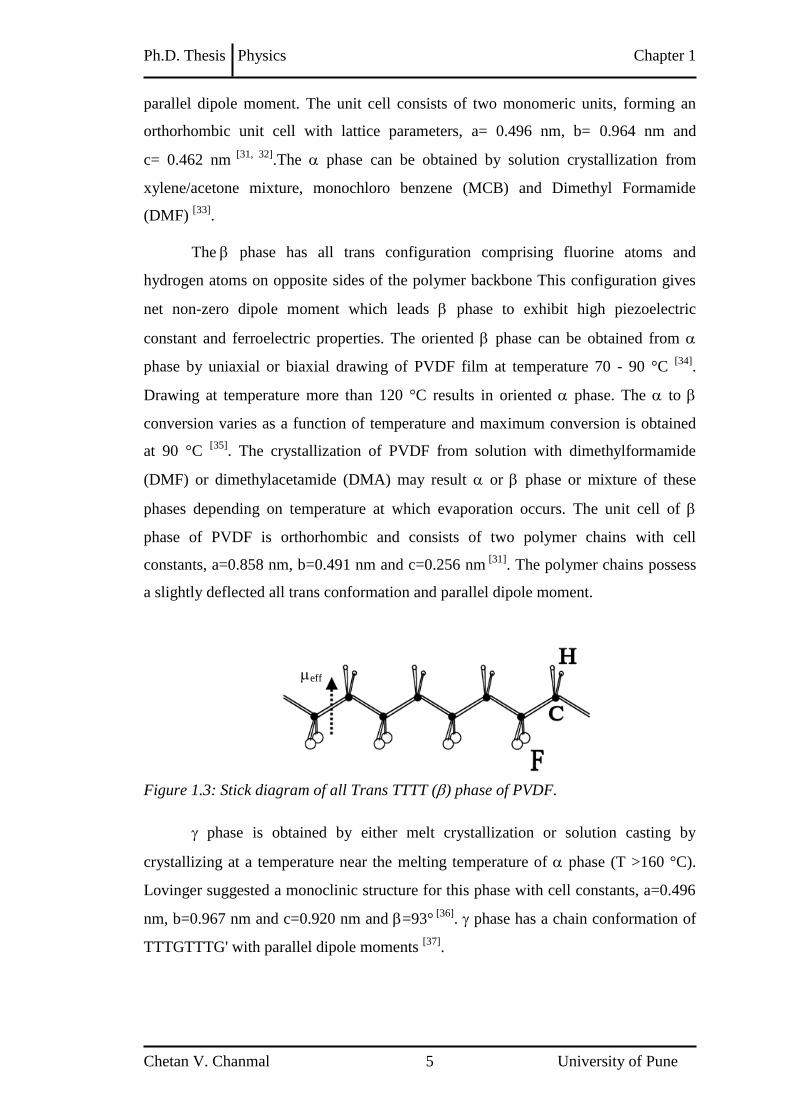
Figure 1.3: Stick diagram of all Trans TTTT () phase of PVDF.
phase is obtained by either melt crystallization or solution casting by
crystallizing at a temperature near the melting temperature of phase (T >160 °C).
Lovinger suggested a monoclinic structure for this phase with cell constants, a=0.496
nm, b=0.967 nm and c=0.920 nm and =93° [36]
. phase has a chain conformation of
TTTGTTTG' with parallel dipole moments [37]
.
eff
Ph.D. Thesis Physics Chapter 1
Chetan V. Chanmal 6 University of Pune
Properties of PVDF
Crystallinity:
The commercial grade PVDF is about 40-50 % crystalline. The heat of fusion
of 100 % crystalline PVDF is 25 Cal/g [38]
.
Thermal properties:
PVDF is thermally stable up to temperature 470 °C beyond which it degrades
with pronounced loss of mass, nearly 60 %. The degradation is due to the emission of
hydrogen fluoride along with a small amount of C4H3F3. Above 600 °C a residual
mass closer to 20 % is observed corresponding to the cross-linked material. The glass
transition temperature is found to be about − 60 °C from dynamic mechanical analysis
(DMA) and differential scanning calorimetry (DSC) experiments. The melting
temperature of PVDF lies in the range of 160 °C to 180 °C depending on the type
crystalline phase. The melting temperature is lower than the Curie temperature (Tc) of
PVDF calculated in the range 205 to 208 °C. This indicates that heating the poled
PVDF films to temperatures lower than the melting temperature induces important
conformational changes, but not a complete phase transition and thus not a complete
depolarization of the polymer.
Piezoelectric properties:
Piezoelectric material is one which undergoes changes in electrical
polarization in response to mechanical stress (or vice versa). This property can further
extended to distinguish two important related properties i.e. pyroelectricity and
ferroelectricity. In 1969, Kawai found high piezoelectric activity in polarized PVDF
and many potential applications of PVDF were explored since then. PVDF exhibits by
far strongest piezoelectric and pyroelectric property of all known polymers [39]
.
Moreover, piezoelectric polymer is considered superior over conventional
piezoelectric ceramics as they offer ease of process and flexibility of polymer matrix.
The acoustic impedance of piezoelectric polymer is low which matches closely with
water, living tissue and other organic materials. Owing to their low acoustic
impedance, they have been also used as materials for broadband energy convertors[40]
.
Ferroelectric properties:
Ferroelectric polymer thin films have great potential for applications in
microelectromechanical systems and solid state electronic memories. The origin of

Ph.D. Thesis Physics Chapter 1
Chetan V. Chanmal 7 University of Pune
ferroelectric properties in PVDF lies in the internal crystal structure imparting
nonzero dipole moment due to high electronegative fluorine atom and orientation of
crystalline dipole in the preferred direction. Polar PVDF (, , phases) exhibits
ferro-electric properties. The long-range order interaction of dipoles in the
ferroelectric phase is extremely strong. Therefore, the Curie temperature (TC) of
220 °C is higher than the melting point (Tm) [25]
.
Pyroelectric property:
Pyroelectricity in PVDF was first observed by Bergman et al. in 1971. PVDF
is strong absorber of infrared energy in the wavelength region of 7-20 m [41]
. This
wavelength region covers same wavelength region of human body. Therefore, PVDF
makes natural choice of material useful in human motion sensor and pyroelectric
sensor in sophisticated instruments like night vision cameras and laser beam profiling
sensors.
Dielectric Property:
PVDF is known for its unique dielectric properties. The unique dielectric
properties of PVDF based nanocomposites originates from the presence of highly
electronegative fluorine on the polymer chains and the alignment of the C-F dipole in
the direction of applied electric field. The dielectric permittivity of PVDF is close to 9
for non-polar phase and around 10-12 for polar phase. Several dielectric
relaxations are seen in PVDF. The a relaxation, corresponding to the segmental
motion in amorphous phase of PVDF, is observed at − 40 °C [42]
. This peak maxima
shifts towards lower frequency with decreasing temperature along with a broadening.
The c-transition observed at approximately 80 °C of PVDF is due to the relaxation
within the crystalline phase [43]
. As temperature increases the magnitude of the loss
peak increases and shifts to higher frequencies. This c relaxation is observed only in
the case of phase PVDF. Third relaxation is observed in the low frequency which is
ascribed to the Maxwell-Wagner-Sillars (MWS) relaxation. The MWS relaxation is
observed due to difference in the conductivity and permittivity values of the
crystalline and amorphous phases.
Along with above mentioned properties, PVDF is known for its heat resistant,
flame resistance and thermally stable engineering polymer. It is highly weather
resistant, and is resistant to most of the chemicals.
Ph.D. Thesis Physics Chapter 1
Chetan V. Chanmal 8 University of Pune
1.4 Nanomaterials
Before discussing properties of nanocomposites, it is important to understand
the advantages offered by nanofillers compared to large sized fillers. The first obvious
difference between conventional composites materials and nanocomposites is the size
of the filler. Nanoparticles are, by definition, particles with diameters below the
micron dimension: generally, below 0.1 μm (100 nm). A more stringent definition
considers nanoparticles as particles with properties depending directly on their size.
Examples are optical, electrical, or magnetic properties. The reduced filler size leads
to a large increase in their specific area and as a consequence this influences filler
polymer interactions [44, 45]
. Because of the very high values of specific surface area in
nanomaterials, the relative number of molecules close to the surface is very high,
which leads to significant variations of their electronic, optical, electro-magnetic and
thermodynamic or mechanical properties and behavior [46-50]
. In other words, the
amount of nanofiller incorporated into polymer matrix is considerably lower
compared to micron sized fillers to achieve the similar improvement of properties.
Thus, the important advantage that these nanocomposites have is the various property
enhancements are all achieved at very low filler content of 5 vol% [51, 52]
. Hence, in
most cases, clarity and polymer processability are unaffected.
Along with the individual properties of the host material and fillers, interfacial
region shared by both the components affect properties of nanocomposites. Small size
of nanoparticles provides large interfacial area between particles and host material.
Other factors like aspect ratio of the nanoparticles, filler dispersion in the matrix,
physical or chemical interaction of nanoparticles with host material also affect
properties of nanocomposites [53, 54]
. Good dispersion of nanoparticles in the polymer
matrix is the key requirement for attaining superior properties in nanocomposites. The
unique properties of nanocomposites are achieved by interfacial interaction between
polymer and nanofillers. Poor nanofiller/polymer interfacial interactions lead to brittle
materials. Thus, the key factor obtain performing composites is linked to the ability to
finely disperse the nanoparticles and to take a maximum benefit of their large surface
area through strong interfacial adhesion within the polymer matrix.

Ph.D. Thesis Physics Chapter 1
Chetan V. Chanmal 9 University of Pune
1.4.1 Clay
Clays are hydrous aluminum silicates and are generally classified as
phyllosilicates. This consists of natural clays like montmorillonite, hectorite, and
saponite as well as synthetic clays such as magadite, mica, laponite, flourohectorite,
etc [55, 56]
. Montmorillonite is the clay by far most commonly used in polymer layered
silicate nanocomposite. Montmorillonite has a general formula (M+y. n H2O) (Al2-y
Mgy) Si4 O10 (OH)2). M+ is the exchangeable cation (monovalent ion) and nH2O
includes the interlayer water not specifically associated with ions. Crystal structure
consists of layers made up of two tetrahedrally coordinated silicon atoms fused to an
edge-shared octahedral sheet of either aluminum or magnesium hydroxide. The layer
thickness is around 1 nm, and the lateral dimensions of these layers may vary from 30
nm to several microns or larger, depending on the particular layered silicate. When
these high aspect ratio nanoparticles are dispersed in a polymer, they can be either,
intercalated by the polymer chains, or, individually exfoliated within the polymer
matrix. Stacking of the layers leads to a regular Van der Waals gap between the layers
called the interlayer or gallery. Isomorphic substitutions within the layers (for e.g.,
Al3+
replaced by Mg2+
or Fe2+
replaced by Li+) generate negative charges that are
counterbalanced by alkali or alkaline earth cations located between the platelets or in
the galleries as shown in figure 1.4. Chemical modification of clay is required for
making it dispersible in polymer matrix. The properties of polymer/clay
nanocomposites are governed by the level of dispersion of clay in the polymer matrix.
Figure 1.4: Structure of Montmorillonite clay [7]
.
Ph.D. Thesis Physics Chapter 1
Chetan V. Chanmal 10 University of Pune
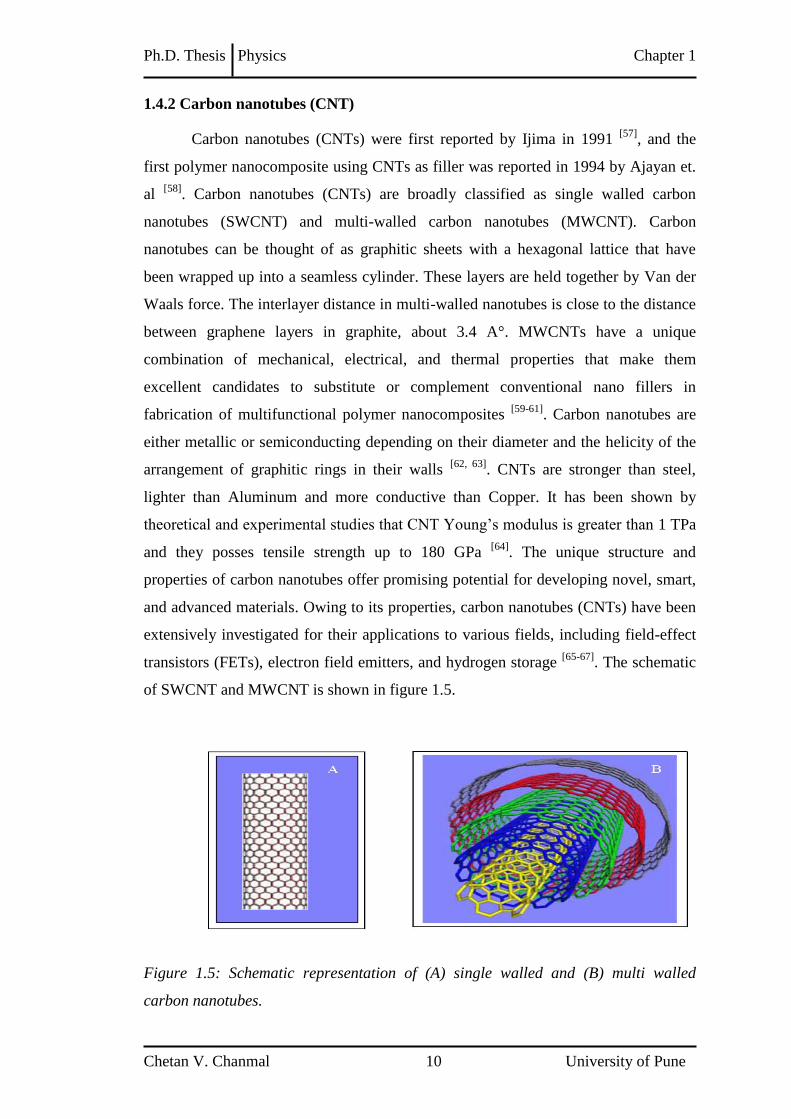
1.4.2 Carbon nanotubes (CNT)
Carbon nanotubes (CNTs) were first reported by Ijima in 1991 [57]
, and the
first polymer nanocomposite using CNTs as filler was reported in 1994 by Ajayan et.
al [58]
. Carbon nanotubes (CNTs) are broadly classified as single walled carbon
nanotubes (SWCNT) and multi-walled carbon nanotubes (MWCNT). Carbon
nanotubes can be thought of as graphitic sheets with a hexagonal lattice that have
been wrapped up into a seamless cylinder. These layers are held together by Van der
Waals force. The interlayer distance in multi-walled nanotubes is close to the distance
between graphene layers in graphite, about 3.4 A°. MWCNTs have a unique
combination of mechanical, electrical, and thermal properties that make them
excellent candidates to substitute or complement conventional nano fillers in
fabrication of multifunctional polymer nanocomposites [59-61]
. Carbon nanotubes are
either metallic or semiconducting depending on their diameter and the helicity of the
arrangement of graphitic rings in their walls [62, 63]
. CNTs are stronger than steel,
lighter than Aluminum and more conductive than Copper. It has been shown by
theoretical and experimental studies that CNT Young’s modulus is greater than 1 TPa
and they posses tensile strength up to 180 GPa [64]
. The unique structure and
properties of carbon nanotubes offer promising potential for developing novel, smart,
and advanced materials. Owing to its properties, carbon nanotubes (CNTs) have been
extensively investigated for their applications to various fields, including field-effect
transistors (FETs), electron field emitters, and hydrogen storage [65-67]
. The schematic
of SWCNT and MWCNT is shown in figure 1.5.
Figure 1.5: Schematic representation of (A) single walled and (B) multi walled
carbon nanotubes.

Ph.D. Thesis Physics Chapter 1
Chetan V. Chanmal 11 University of Pune
1.4.3 Barium Titanate (BaTiO3)
The ceramic Barium Titanate (BaTiO3) is perhaps the most widely
investigated oxide in the field of dielectrics. It has been attracted considerable interest
for its wide variety of applications. The high dielectric constant of BaTiO3 makes it
suitable for applications like multilayer ceramic capacitors (MLCCs), dynamic
random access ferroelectric memories (DRAMs), etc. BaTiO3 also exhibits attractive
piezoelectric properties useful for a large area of applications such as nonvolatile
memories, surface acoustic wave devices, tunable capacitors, pyroelectric detectors,
etc. However, major disadvantage of BaTiO3 is the requirement of high temperature
during its processing.
Barium titanate belongs to a group of materials that crystallize with the
perovskite structure having the general composition of ABO3. Barium titanate exists in
the paraelectric cubic phase above its Curie temperature of about 130 °C, while in the
temperature range of 0 °C to 130 °C, the ferroelectric tetragonal phase is stable [68]
.
The important dielectric properties of BaTiO3 arise from a structural change where the
center Ba2+
and Ti4+
cations are displaced relative to the O2-
ions, leading to the
formation of electric dipoles (Figure 1.6). This leads to net dipole moment produced
per unit volume for the dipoles pointing in a given direction.
BaTiO3 nanoparticles are synthesized by using number of methods, such as,
hydrothermal method, sol-gel processing, flame assisted spray pyrolysis (FASP),
radio-frequency plasma chemical vapor deposition (RF-plasma CVD), and
electrochemical route [69-73]
.
Figure 1.6: Crystal structure of BaTiO3 above the Curie temperature is cubic (left)
and below the Curie temperature is tetragonal (right).
Ba2+
O2-
Ti4+
Ph.D. Thesis Physics Chapter 1
Chetan V. Chanmal 12 University of Pune
1.5 PVDF based Nanocomposites
PVDF is studied with various nanofillers having different morphology and
dimensions in nanoscale. The nanofillers addition to PVDF is used for variety of
reasons: cost reduction, improved processing, thermal conductivity, electrical
property, magnetic property and high dielectric material. For example fillers such as
FeCl2 and MnCl2 are used to provide better electrical and magnetic properties [74]
.
Below we discuss some important nanocomposites systems based on PVDF.
As mentioned earlier, phase can be easily obtained from melt crystallization
and is more stable compared to phase. Generally, it is difficult to obtain phase
PVDF film and many attempts were made to stabilize the phase. In order to enhance
the phase content, which will provide the important properties of PVDF for various
applications, making composites of PVDF with other organic or inorganic fillers was
studied extensively. Nanocomposites of PVDF with organically modified silicates
were shown to crystallize PVDF into phase. Priya and Jog first reported the
stabilization of phase of PVDF in nanocomposites with the addition of clay [75, 76]
.
The thermal annealing studies indicated the stable phase in these nanocomposites.
The addition of clay also found to improve the mechanical properties of
nanocomposites. Wu et al. studied nanocomposite of Poly (vinylidene fluoride)
(PVDF) with graphene sheets (GSs) [77]
. The structure-properties relationships of
PVDF/GSs nanocomposites were studied using differential scanning calorimetry and
X-ray diffraction. The addition of GSs to the PVDF matrix promotes phase to
phase transformation of the polymer crystal. The nanocomposites also found to
exhibit significant increases in mechanical properties and thermal stability compared
to the neat PVDF. Addition of MWCNT to PVDF has demonstrated remarkable
improvement properties, not only dielectric permittivity but also mechanical, thermal
and piezoelectric properties [78]
. In case of MWCNT based nanocomposites,
dispersion of MWCNT is important factor which determines the final properties
achieved in the nanocomposites. Hong et al. studied the piezoelectric properties of
solution blended MWCNT and PVDF nanocomposites [79]
. For drawn samples, the β
phase content increased with increasing MWCNT loading. With the addition of poling
process, pure phase has been obtained at 0.2 wt% loading of MWCNT. The
presence of MWCNT in PVDF matrix plays a role of nucleating agent for the

Ph.D. Thesis Physics Chapter 1
Chetan V. Chanmal 13 University of Pune
crystallization of phase PVDF and hence the enhancement in the properties. Levi et
al., have shown that to conversion of PVDF occurs in solution blended
PVDF/Carbon nanotube composites and the ratio between these two crystalline
phases varies depending on the weight % of Carbon nanotubes [80]
. The nanofillers
MgNO3 and AgNO3 were used to promote tophase of PVDF and to increase the
electric conduction in the nanocomposites [81]
. In other work CuCl2 based
nanocomposites were used to promote the phase in PVDF. Recently,
electrospinning of PVDF nanofibers shows phase formation [82]
. The high voltage
during electrospinning acts like poling filed to PVDF which helps in crystallization of
phase PVDF.
The electronic packaging industry requires thermally conductive but
electrically insulating polymer composites. The composites of PVDF with aluminium
nitride and silicon nitride were studied in this context. The highest thermal
conductivity of 11.5 W/mK was obtained with PVDF and aluminium nitride [83]
.
Various nanofillers were added to PVDF to increase the dielectric permittivity
of PVDF. Electroactive ceramics like lead zirconate titanate (PZT) and BaTiO3 are
useful for this purpose [84]
. These ceramics possess very high dielectric permittivity at
relatively low dielectric losses. However they have drawbacks like high temperature
is required for synthesis, poor flexibility and not suitable for large area synthesis. PZT
and BaTiO3 were added to PVDF to get piezo and pyroelectric transducers. These
composites are important in various applications as they combine important feature of
individual components and their property can be tailored to various requirements.
These nanocomposites are also useful in the development of sensors and actuators.
The dielectric permittivity was also increased to high value in these nanocomposites.
A three-phase composite with multi-walled carbon nanotubes (MWNTs) and BaTiO3
particles embedded into Polyvinylidene fluoride was prepared by using a simple
blending and hot-molding technique by Dang et al [85]
. The results show that dielectric
permittivity increases rapidly when the concentration of MWCNT is close to
percolation threshold. In another alternative approach, semiconducting nanofillers
were added into PVDF matrix to increase dielectric permittivity with low conductivity
level. Nan et al. studied the Bi2S loaded PVDF nanocomposites [86]
. The preferential
orientation of Bi2S rods led to the anisotropic electric properties.

Ph.D. Thesis Physics Chapter 1
Chetan V. Chanmal 14 University of Pune
The ever increasing demand of energy from modern society is perhaps the
greatest challenges that mankind will continue to face. Over the past decades
intensive research efforts have been carried out in developing energy harvesting
system. Several efforts were demonstrated for mechanical energy harvesting using
PVDF based nanofibers membranes [87, 88]
. Most of them were based on piezoelectric
effect. Electrospun PVDF nanofibers were directly used as active layer to make
mechanical to electrical energy conversion devices. The device was also useful for
driving electronic device and shows long term stability. Piezoelectric PVDF is a good
alternative material for fabricating flexible generators. Piezoelectric polymer
nanofibers also offers better flexibility in comparison to the inorganic nanowires.
Although PVDF has poorer piezo property than PZT, they offer unique advantage in
fabrication of flexible nanogenerators [89]
.The piezoelectric coefficients of ~ − 20 to
30 (d33) and ~ 18 (d31) pC/N are reported for phase PVDF, which is sufficient to
generate appreciable voltage under strain [90]
. The biocompatibility of PVDF also
allows to use in biological system for energy harvesting.
In recent year significant interest in molecular electronics and organic
compounds based devices has taken place. Due to its ferroelectric properties, PVDF is
one of the most promising candidates for applications in information storage medium
among various non-volatile organic memories. The basic principle of operation in this
device is bistable electric polarization of gate dielectric, which can be switched by an
applied electric field [91]
. The present motivation in OFET is driven to search for SiO2
alternative which can significantly reduce the operating voltage [92]
. Therefore, choice
of gate dielectric material is important parameter to fully utilize applications of
OFET. In this context, PVDF and its copolymers are extensively investigated as gate
dielectric material in OFET architecture. These OFET showed mobility comparable to
conventional silicon base FET and high on/off ratio.
Mhaisalkar et al. fabricated ferroelectric thin film transistor using Pentacene as
semiconducting layer and P(VDF-TrFE) copolymer as gate insulator [93]
. The
transistor devices exhibited a generally observed clockwise hysteresis of drain current
during the sweeping of gate voltage, which indicates the memory effects by dipole
moment in P (VDF-TrFE) layer. They have also found positive turn on voltage shift
up to +25 V when the gate bias was swept from ON to OFF state. This observed shift
was attributed to the surface dipole field, trap states in semiconductor, and surface

Ph.D. Thesis Physics Chapter 1
Chetan V. Chanmal 15 University of Pune
roughness due to high remnant dipolar polarization of P (VDF-TrFE). Cheomlin park
et al. used spin coated PVDF thin films to fabricate ferroelectric OFET [94]
. The
device shows a drain current bistablility of 100 A at zero gate voltage with ±20 V
gate voltage sweep. Ideal characteristics of a gate dielectric are that it should be
solution processable at room temperature, flexible and should possess high dielectric
constant. Feng Yan et al. fabricated solution processable low voltage OFET with high
dielectric constant PVDF copolymer as relaxor ferroelectric [95]
. The OFET shows
carrier mobility greater that 0.1 cm2 V
-1s
-1 at gate voltage of 3 V.
Functional materials can be directly integrated into OFET device to get several
applications of OFET. Organic thin film transistors and ferroelectric polymer
(polyvinylidene difluoride) sheet material are integrated to form various sensors for
stress/strain, acoustic wave, and Infrared (heat) sensing applications [96]
. Recent
studies have demonstrated that direct integration functional materials into OFET
device offers a unique way of realizing multimodal devices [97]
.
1.6 Applications of Polymer Nanocomposites
In the past decade polymer nanocomposite materials have been developed and
its several potential applications were been explored in variety of fields including
energy, sensor, transistors, etc. Figure 1.7 shows the important applications of
nanocomposites in diverse fields.
Figure 1.7: Overview of some of the potential applications of polymer
nanocomposites.
Ph.D. Thesis Physics Chapter 1
Chetan V. Chanmal 16 University of Pune
1.6.1 High Dielectric Constant Materials
High energy storage capacitors with high efficiency plays very important role
in the modern electric industry [98]
. To achieve this materials with high permittivity
and high breakdown strength are required, as the energy density of the material is
proportional to the dielectric permittivity and the square of the applied field. Polymers
are suitable choice for high energy density capacitors because of combination of high
breakdown strength and low cost. However, polymers have relatively low dielectric
constant (usually within the range of 2–10) and it is difficult for them to meet the
capacitor requirements. On the other hand, ferroelectric ceramics have high dielectric
constant but suffer from problem like high processing temperatures, brittle nature and
large area synthesis. Currently, research interest is focused on the fabrication of high-
dielectric constant polymer-based nanocomposites. Recently, nanocomposites of
ceramic particles and polymer matrix are fabricated as means of engineering dielectric
property and energy storage capacity [99]
. The basic idea behind this approach is to
integrate complementary properties of each constituent to get substantially enhanced
energy density. The advantage of this method is that, although the breakdown strength
of the polymer/ceramic composites is generally lower than that of pure polymers, the
composites can withstand a relatively high electric field. Different polymer matrix are
used in the nanocomposites are polyethylenes, poly (methyl methacrylate)s, epoxy
resins, and polyimides. These polymers have typically low dielectric constant which
significantly limits energy density obtained in the nanocomposites. Owing to its high
dielectric constant, ferroelectric polymers like PVDF and its copolymer have been
also used for the fabrication of high dielectric constant nanocomposites.
Another popular approach to increase the dielectric permittivity is to add
conducting nanofiller to polymer matrix. Percolative systems consisting of insulating
polymers and conductive fillers can show very high dielectric constants near the
percolation threshold. Dramatic changes in the physical properties of composites
occur when filler particles form a percolating network through the polymer matrix.
So far, numerous percolative composites with high dielectric constants have been
reported [100]
. Typical conductive components include (i) carbon-based fillers such as
carbon black, carbon nanotubes, carbon fiber, graphene, graphite platelets, (ii) metal-
based fillers such as particles and nanowires [101]
.

Ph.D. Thesis Physics Chapter 1
Chetan V. Chanmal 17 University of Pune
The enhancement in the dielectric constant can well described by established
percolation theory. According to percolation theory, the effective dielectric constant ε
of a nanocomposites in percolative system is inversely proportional to the difference
between the volume content of conductive fillers and the percolation threshold, :
According to above equation, a very high dielectric constant can be achieved if the
composites contain an appropriate volume fraction of conductive filler.
Although a very high capacitance or dielectric constant can be realized, the
nanocomposite material cannot withstand a high electric field because of the very
high electrical conductivity of the fillers, resulting in some limitations for certain
applications.
1.6.2 Organic Field Effect Transistor (OFET)
A field-effect transistor (FET) is a three terminal device where the drain
source current (IDS) is modulated and controlled by input voltage at drain electrode
(VDS) and gate electrode (VGS). The metal insulator semiconductor (MIS) structure is
fabricated respectively by gate electrode, gate dielectric and active semiconducting
layer. By controlling the voltage on gate electrode (field effect), charges can be
collected at the semiconductor dielectric interface. These charges are collected across
the conducting channel due to field effect can then be drifted along the channel by
applying a voltage at the drain terminal (VDS). An FET is already referred to as being
organic field effect transistor (OFET), in which the semiconducting layer is merely
composed of organic molecules or polymers, although all components may be
replaced by organic materials.
Unlike silicon based transistors, organic thin film transistors can be fabricated
at room temperature and a variety of substrates can be used. The main difference
between organic and inorganic device is that OFET works in accumulation mode, i.e.
conduction mainly occurs in the ON state of device. Without a gate voltage being
applied, no current flows between the source and drain electrode, the device is in OFF
state. In the ON state, charge carriers are formed within few angstroms of the
semiconductor dielectric interface when the gate voltage is applied. These charges are
of same type of majority carriers in the semiconductor. Despite of this fundamental

Ph.D. Thesis Physics Chapter 1
Chetan V. Chanmal 18 University of Pune
difference, the basic equations describing operation of device resembles those of
inorganic FET and can be applied to organic FET.
Operating mode
Most OFETs reported in the literature so far exhibit either p-type or n-type
behavior, meaning that the charge carriers are either holes or electrons respectively.
p-type OFETs comprise the majority of these devices, showing the best transport
properties and considerably more stable than n-type devices [102]
. However, very
recently, few groups [103, 104]
have shown that ambipolar charge transport is also quite
achievable and is a generic property of the organic semiconductors.
As stated earlier, the OFETs mainly works in accumulation mode. In hole
transporting devices, a negative voltage is applied to the gate, inducing holes at the
source electrode. These positive charge carriers will be injected into the
semiconductor layer, provided that the hole injection barrier between the Fermi level
of the metal and the highest occupied molecular orbital (HOMO) of the
semiconductor is low. These accumulated holes form a conducting channel at the
organic semiconductor/insulator interface. By applying a second negative bias to the
drain (VDS), the charges move along the channel and are collected at the drain.
OFETs are generally prepared in two configurations: The bottom-gate and the
top - gate configuration as shown in Figure 1.8 (a). Bottom gate- top contact is
favored over the top gate-bottom contact configuration because bottom contact has
higher resistance, which reduces the output current due to poor growth of
semiconductor on electrode surfaces. Also top contact device has larger contact area
between the electrodes and the semiconductor which allows for more effective charge
injection into the organic semiconductor. However, patterning of metal electrodes on
top of semiconductor requires controlled metal evaporation in order to avoid damage
of polymer film during deposition. Figure 1.8 (b) presents the schematic of device
architecture in top contact geometry showing the channel width (W) and length (L).
Ph.D. Thesis Physics Chapter 1
Chetan V. Chanmal 19 University of Pune
Bottom - gate
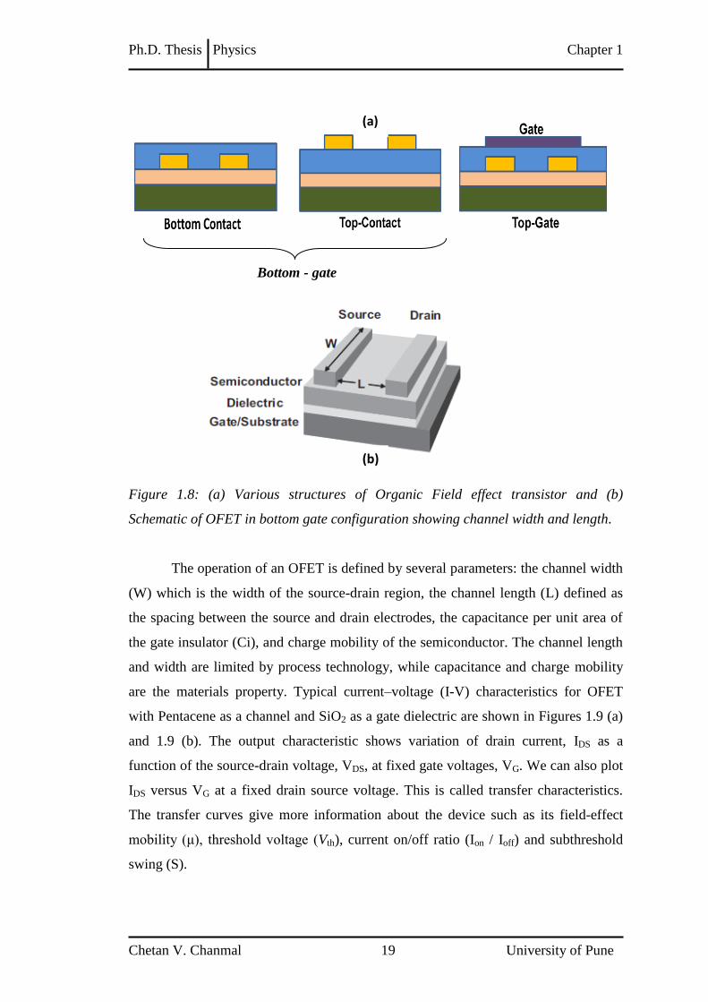
Figure 1.8: (a) Various structures of Organic Field effect transistor and (b)
Schematic of OFET in bottom gate configuration showing channel width and length.
The operation of an OFET is defined by several parameters: the channel width
(W) which is the width of the source-drain region, the channel length (L) defined as
the spacing between the source and drain electrodes, the capacitance per unit area of
the gate insulator (Ci), and charge mobility of the semiconductor. The channel length
and width are limited by process technology, while capacitance and charge mobility
are the materials property. Typical current–voltage (I-V) characteristics for OFET
with Pentacene as a channel and SiO2 as a gate dielectric are shown in Figures 1.9 (a)
and 1.9 (b). The output characteristic shows variation of drain current, IDS as a
function of the source-drain voltage, VDS, at fixed gate voltages, VG. We can also plot
IDS versus VG at a fixed drain source voltage. This is called transfer characteristics.
The transfer curves give more information about the device such as its field-effect
mobility (μ), threshold voltage (Vth), current on/off ratio (Ion / Ioff) and subthreshold
swing (S).
(a)
(b)

Ph.D. Thesis Physics Chapter 1
Chetan V. Chanmal 20 University of Pune
Figure 1.9: (a) Output and (b) transfer characteristics of Pentacene/SiO2 OFET.
The output curves show the gate modulation of source–drain current (IDS).
According to the common model of OFETs, in the linear regime (at low VDS (< VGS −
Vth)), μ (which has units of cm2 V
− 1 s
− 1) can be calculated from the following
equation:
The value of μ of the OFETs in the saturation region (at high VDS (> VGS −
Vth)) is given by:
Where, is the capacitance per unit area of the gate dielectric layer, and L and W are
the channel length and width, respectively. From this equation, it is obvious that μ
will be gate-voltage dependent, if the relationship between IDS and VG is nonlinear.
Although it is expected that the linear regime and the saturation regime μ values to be
similar for a device, this is not always the case. Source and drain contact resistances
or high electric fields often affect the linear regime mobilities.
(a) (b)
Ph.D. Thesis Physics Chapter 1
Chetan V. Chanmal 21 University of Pune
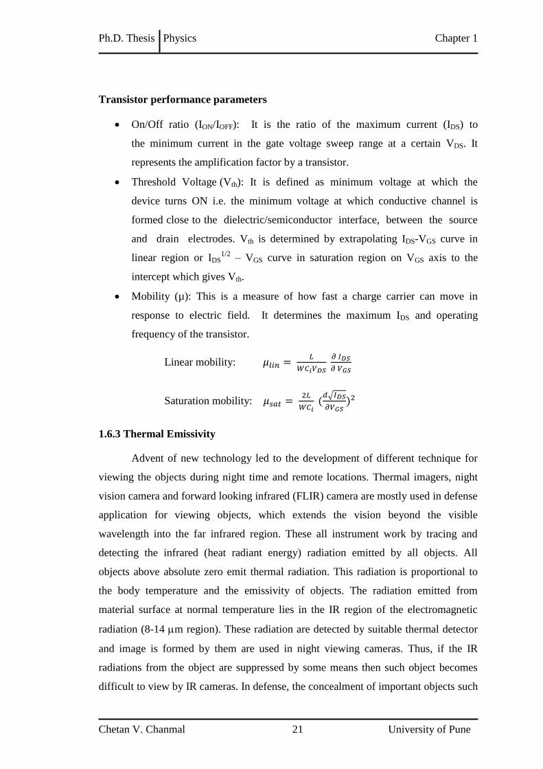
Transistor performance parameters
On/Off ratio (ION/IOFF): It is the ratio of the maximum current (IDS) to
the minimum current in the gate voltage sweep range at a certain VDS. It
represents the amplification factor by a transistor.
Threshold Voltage (Vth): It is defined as minimum voltage at which the
device turns ON i.e. the minimum voltage at which conductive channel is
formed close to the dielectric/semiconductor interface, between the source
and drain electrodes. Vth is determined by extrapolating IDS-VGS curve in
linear region or IDS1/2
– VGS curve in saturation region on VGS axis to the
intercept which gives Vth.
Mobility (µ): This is a measure of how fast a charge carrier can move in
response to electric field. It determines the maximum IDS and operating
frequency of the transistor.
Linear mobility:
Saturation mobility:
1.6.3 Thermal Emissivity
Advent of new technology led to the development of different technique for
viewing the objects during night time and remote locations. Thermal imagers, night
vision camera and forward looking infrared (FLIR) camera are mostly used in defense
application for viewing objects, which extends the vision beyond the visible
wavelength into the far infrared region. These all instrument work by tracing and
detecting the infrared (heat radiant energy) radiation emitted by all objects. All
objects above absolute zero emit thermal radiation. This radiation is proportional to
the body temperature and the emissivity of objects. The radiation emitted from
material surface at normal temperature lies in the IR region of the electromagnetic
radiation (8-14 m region). These radiation are detected by suitable thermal detector
and image is formed by them are used in night viewing cameras. Thus, if the IR
radiations from the object are suppressed by some means then such object becomes
difficult to view by IR cameras. In defense, the concealment of important objects such
Ph.D. Thesis Physics Chapter 1
Chetan V. Chanmal 22 University of Pune
as military equipments or vehicles from infrared detection is necessary for the
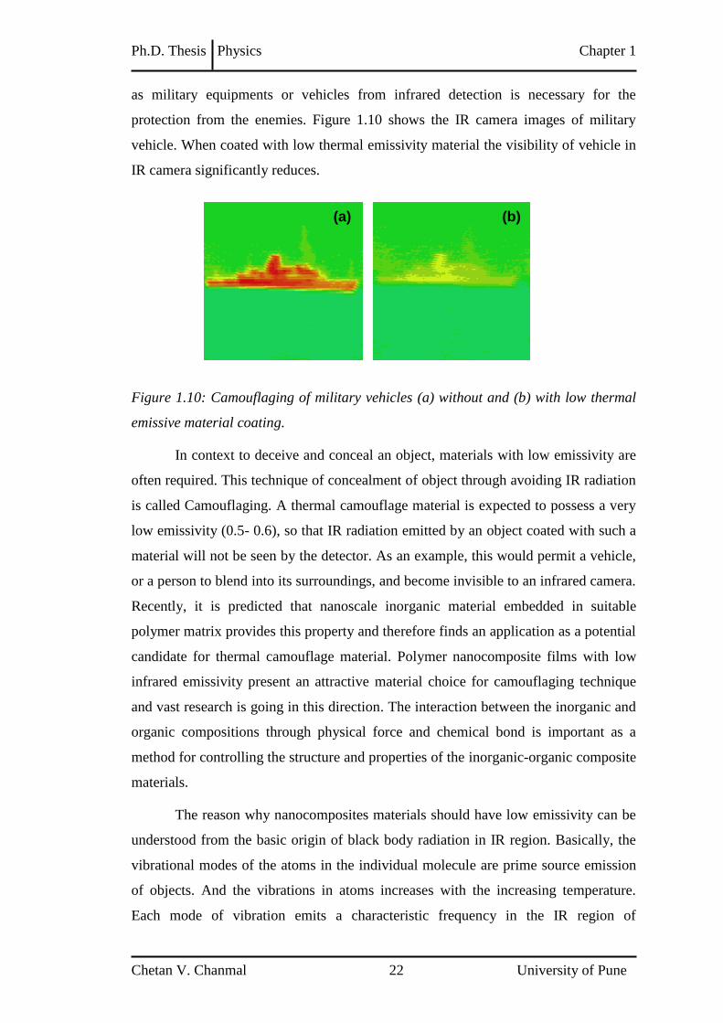
protection from the enemies. Figure 1.10 shows the IR camera images of military
vehicle. When coated with low thermal emissivity material the visibility of vehicle in
IR camera significantly reduces.
Figure 1.10: Camouflaging of military vehicles (a) without and (b) with low thermal
emissive material coating.
In context to deceive and conceal an object, materials with low emissivity are
often required. This technique of concealment of object through avoiding IR radiation
is called Camouflaging. A thermal camouflage material is expected to possess a very
low emissivity (0.5- 0.6), so that IR radiation emitted by an object coated with such a
material will not be seen by the detector. As an example, this would permit a vehicle,
or a person to blend into its surroundings, and become invisible to an infrared camera.
Recently, it is predicted that nanoscale inorganic material embedded in suitable
polymer matrix provides this property and therefore finds an application as a potential
candidate for thermal camouflage material. Polymer nanocomposite films with low
infrared emissivity present an attractive material choice for camouflaging technique
and vast research is going in this direction. The interaction between the inorganic and
organic compositions through physical force and chemical bond is important as a
method for controlling the structure and properties of the inorganic-organic composite
materials.
The reason why nanocomposites materials should have low emissivity can be
understood from the basic origin of black body radiation in IR region. Basically, the
vibrational modes of the atoms in the individual molecule are prime source emission
of objects. And the vibrations in atoms increases with the increasing temperature.
Each mode of vibration emits a characteristic frequency in the IR region of
(a) (b)

Ph.D. Thesis Physics Chapter 1
Chetan V. Chanmal 23 University of Pune
electromagnetic spectrum. This emission can be suppressed either by reducing the
temperature or by reducing the extend of atomic vibrations. In nanocomposites, the
incorporation of nanoparticles is expected to increase lattice constant or internuclear
distance between the atoms and therefore reducing the force constant of vibrational
modes [105]
. This ultimately shifts the frequency of vibration into longer frequency
region and hence reducing the thermal emissivity. Also, the understanding of thermal
emissivity is important as it serves important intrinsic thermo physical property of
material in the energy balance [106]
.
In recent years, application of functional nanomaterials for low emissivity
application attracted extensive attention. The reduction in the emissivity value is made
possible by the use of different types of functional nanofillers. Apart from high aspect
ratio of these nanoparticles, their unusual physiochemical and optoelectronic
properties have led to their useful application. Indium tin oxide (ITO), silicon based
nanomaterials are commonly used materials for the low emissivity application.
Especially, Collagen-g-PMMA/In2O3 nanocomposite found to exhibit lower infrared
emissivity, however due its low decomposition temperature puts limit on the end use
of this material. Some authors studied the use of BaTiO3 for low emissivity
application [107]
. The incorporation of BaTiO3 into silicon containing polyimide has
found to affect the emissivity of nanocomposites. This decrease in emissivity was
attributed to the presence of interfacial interaction between silicon containing polymer
and BaTiO3 nanoparticles.
1.7 Research Objectives
The primary objective of this thesis is to fabricate novel polymer
nanocomposites based on PVDF using three different commercially available
nanofillers viz. organically modified layered silicates , MWCNTs, and BaTiO3. Three
different techniques of were used to fabricate the polymer nanocomposites. Melt
mixing technique is used for PVDF/BaTiO3, pulsed laser deposition for PVDF/
MWCNT nanocomposites, spin coating is used for PVDF/Clay nanocomposites.
The specific objectives of this dissertation are:
To fabricate nanocomposites based on PVDF and organo–inorganic nanofiller
having various dimensions in nanoscale viz. MWCNTs, BaTiO3 and clay.
Ph.D. Thesis Physics Chapter 1
Chetan V. Chanmal 24 University of Pune
To study the effect of addition of nanofiller on the crystal structure of PVDF and
dielectric properties of PVDF.
To study the application of PVDF/BaTiO3 nanocomposites for low thermal
emissivity camouflaging material.
To study the applications of PVDF/MWCNT nanocomposites as an active channel
layer in field effect device.
To fabricate OFET using PVDF/Clay nanocomposites as gate dielectric layer and
to study the memory retention and IR sensing applications of OFET.
1.8. Structure of the Thesis
The entire research work is presented in six chapters.
Chapter 1 provides the importance of PVDF and its properties. A brief overview of
polymer nanocomposites and their applications relevant to thesis are also discussed.
Chapter 2 describes various methods used for the fabrication of polymer
nanocomposites. This chapter also includes details of basic theoretical background of
various characterization techniques used for PVDF nanocomposites.
Chapter 3 presents fabrication of PVDF/BaTiO3 nanocomposites by simple melt
mixing technique. The effect of BaTiO3 nanoparticles on the dielectric properties of
PVDF is studied. Further, the fabrication of nanofibers by electrospinning and their
potential application for camouflaging technique is also discussed.
Chapter 4 presents fabrication of thin films of PVDF/MWCNT nanocomposites by
Pulsed Laser Deposition (PLD). The addition of MWCNT on the dielectric and
conductivity properties were presented in this chapter. The use of PVDF/MWCNT
nanocomposite as an active channel layer in OFET device is discussed.
Chapter 5 presents the dielectric properties of PVDF/Clay nanocomposites. The
application of PVDF/clay nanocomposite as dielectric layer in OFET configuration is
described. Further, the application of OFET as memory retention and IR sensing
abilities is studied.
Chapter 6 summarizes the work described in this thesis by presenting the salient
features of the work and also presents the possible avenues for future work
Ph.D. Thesis Physics Chapter 1
Chetan V. Chanmal 25 University of Pune
1.9 References
1. D.Y.Godovsky, Advances in polymer sciences, 2000, 153, 165-204.
2. Rolf E. Hummel, “Understanding Materials Science: History, Properties,
Applications”, Springer, 2nd ed. 2005.
3. C. Velasco-Santos, A. L. Martinez-hernandez, V. M. Castano, Composite
Interfaces, 2005, 11, 567 – 586.
4. Hatsuo Ishida, Sandi Campbell, John Blackwell, Chem. Mater., 2000, 12, 1260-
1267.
5. Philippe Dubois, Michaël Alexandre, Advanced Engineering Mater., 2006,
8,147-154.
6. D.R. Paul, L.M. Robeson, Polymer, 2008, 49, 3187–3204.
7. Suprakas Sinha Ray, Masami Okamoto, Prog. Polym. Sci., 2003, 28, 1539–
1641.
8. T. J. Pinnavaia, Science, 1983, 220, 365-371.
9. A. Usuki, Y. Kojima, M. Kawasumi, A. Okada, Y. Fukushima, T. Kurauchi, O.
Kamigatio, J. Mater. Res., 1993, 8, 1179.
10. K. Yano, A. Usuki, A. Okada, T. Kurauchi, O. Kamigatio, J. Polym. Sci. Part A:
Polym. Chem., 1993, 31, 2493.
11. P. B. Messersmith, E. P. Giannelis, Chem. Mater., 1994, 6, 1719.
12. A. Okada, A. Usuki, Mater. Sci. Eng.: C, 1995, 3, 109.
13. T. Lan, T. J. Pinnavaia, Chem. Mater., 1994, 6, 2216.
14. J. W. Gilman, Appl. Clay. Sci., 1999, 15, 31.
15. Del K. Strawhecker, E. Manias, Chem. Mater., 2000, 12, 2943.
16. H. Jeon, H. Jung, S. Lee, S. Hudson, Polym. Bull., 1998, 41, 107.
17. H. Choi, S. Kim, Y. Hyun, M. Jhon, Macromol. Rapid Commun., 2001, 22, 320.
18. Jr. R. Gregorio, E. M. Ueno, Journal of Materials Science, 1999, 34, 4489-4500.
19. Jr. R. Gregorio, Journal of Applied Polymer Science, 2006, 100, 3272-3279.
20. Y.Y. Zhang, S.L. Jiang, Y. Yu, G. Xiong, Q.F. Zhang, G.Z. Guang, Journal of
Applied Polymer Science, 2011,123, 2595-2600.
21. T. Umasankar Patro, Milind V. Mhalgi, D.V. Khakhar, Ashok Misra, Polymer,
2008, 49 3486–3499.
22. N. Shukla, A. Shukla, A. K. Takhur, R N P Choudhary, Indian journal of
Engineering and Materials Sciences, 2008, 15, 126-132.

Ph.D. Thesis Physics Chapter 1
Chetan V. Chanmal 26 University of Pune
23. A. Tawansi, A. H. Oraby, S. I. Badr, I. S. Elashmawi, Polym Int., 2004, 53,
370–377.
24. M. A. Marcus, Ferroelectrics, 1982, 40, 29.
25. A. J. Lovinger, Ferroelectrics, 1983, 40, 227.
26. J. Kułek, I. Szafraniak, B. Hilczer, M. Połomska, Journal of Non-Crystalline
Solids, 2007, 353, 4448-4452.
27. Chengliang Sun, Jian Shi, Dylan J. Bayerl, Xudong Wang, Energy Environ. Sci.,
2011, 4, 4508-4512.
28. Qi-Dan Ling, Der-Jang Liaw, Chunxiang Zhu, Daniel Siu-Hung Chan, En-Tang
Kang, Koon-Gee Neoh, Progress in Polymer Science, 2008, 33, 917–978.
29. A Kimoto, N Sugitani, Meas. Sci. Technol., 2010, 21, 075202.
30. Y. Takahashi, A. Tadokoro, Macromolecules, 1980, 13, 1318.
31. M. A. Bachman, J.B. Lando, Macromolecules, 1981, 14, 40.
32. L. Kutschabsk, E. Hohne, R. G. Kretschmer, Acta polymerica, 1991, 43, 357.
33. R. Hasegawa, Y. Takahashi, Y. Chatani, H. Tadokoro, Polymer Journal, 1972,
3, 600.
34. C. C. Hsu, P. H. Geil, Journal of Material Science, 1989, 24, 1219.
35. P.Sajkiewicz, A. Wasiak, Z. Goclowski, European polymer journal, 1999, 35,
423.
36. J. H. Wendroff, Journal of Polymer Science: Polymer Letters, 1980, 18, 439.
37. A. J. Lovinger, Journal of Polymer Science: Polymer Physics, 1980, 18, 793.
38. H. Nagawada, Y. Ishida, Journal of Polymer Physics, 1973, 11, 2153.
39. J. Strathdee, W. H. Robinson, Journal Applied Physics, 1982, 53, 605.
40. W. T. Chen, E. Sacher, D. H. Strope, J. J. Woods, Journal of Macromolecular
Science Part B:,1982, 21, 397.
41. Jacob Fraden, Handbook of Modern Sensors Physics, Designs, and Applications,
Fourth edition, Springer, London, 2010.
42. N. G. Mccrum, B. E. Read, G. William, “Anelastic and dielectric effects in
Polymeric solids”, John Wiley and sons, 1967.
43. B. Hahn, J. Wendroff, D. Y. Yoon, Macromolecules, 1985, 18,718.
44. Emil Roduner, Chem. Soc. Rev., 2006, 35, 583–592.
45. G. Cao, “Nanostructures and Nanomaterials: Synthesis, Properties and
Applications”, Imperial College Press, 2004.

Ph.D. Thesis Physics Chapter 1
Chetan V. Chanmal 27 University of Pune
46. C. N. R. Rao, Achim Muller, Anthony K. Cheetham, “The Chemistry of
Nanomaterials”, John Wiley & Sons, 2006.
47. A. P. Alivisatos, Science, 1996, 271, 933 – 937.
48. Pavel Zrazhevskiy, Xiaohu Gao, Nano Today, 2009, 4, 414 – 428.
49. Vivek Dhas, Subas Muduli, Wonjoo Lee, Sung-Hwan Han, Satishchandra
Ogale, Appl. Phys. Lett. 2008, 93, 243108.
50. Chris Binns, “Introduction to Nanoscience and Nanotechnology”, Wiley, 2010.
51. P. Walter, D. Mader, P. Reichert, R. Mülhaupt, J. Macromol. Sci. Pure. Appl.
Chem. 36A 1999, 1613.
52. L. E. Nielsen, Marcel Dekker, “Mechanical Properties of Polymers and
Composites”, New York, 1974.
53. C.-W. Nan,Y. Shen, Jing Ma, Annu. Rev. Mater. Res., 2010, 40,131–151.
54. Michael E. Mackay, Anish Tuteja1, Phillip M. Duxbury, Craig J. Hawker,
Brooke Van Horn, Zhibin Guan,Guanghui Chen, R. S. Krishnan, Science, 2006,
311, 1740-1743.
55. Philippe Dubois, Michaël Alexandre, Advanced Engineering Materials, 2006, 8,
No. 3
56. E. Giannelis, R. Krishnamoorti, E. Manias, Adv. Poly. Sci., 1999, 138, 107.
57. S. Ijima, Nature (London), 1991, 354, 56.
58. P. M. Ajayan, O. Stephan, C. Colliex, D. Trauth, Science, 1994, 265, 1212.
59. Sandler J, Shaffer M, Prasse T, Bauhofer Q, Schulte K, Windle A,
Polymer,1999, 40, 5967.
60. P. M. Ajayan, Chem. Rev., 1999, 99, 1787-1799.
61. Inpil Kang , Yun Yeo Heung , Jay H. Kim , Jong Won Lee , Ramanand
Gollapudi , Srinivas Subramaniam , Suhasini Narasimhadevara , Douglas Hurd ,
Goutham R. Kirikera , Vesselin Shanov , Mark J. Schulz , Donglu Shi , Jim
Boerio , Shankar Mall , Marina Ruggles-Wren, Composites: Part B, 2006, 37,
382–394.
62. Jeroen W. G. Wildoer, Liesbeth C. Venema, Andrew G. Rinzler, Richard E.
Smalley, Cees Dekker, Nature, 1998, 391, 59-62.
63. Sander J. Tans, Alwin R. M. Verschueren, Cees Dekker, Nature, 1998, 393, 49-
51.
64. T. Uchida, S. Kumar, J. Appl. Polym. Sci. 2005, 98, 985.
65. Bachtold A, Hadley P, Nakanishi T, Dekker C. Science, 2001, 294, 1317.
Ph.D. Thesis Physics Chapter 1
Chetan V. Chanmal 28 University of Pune
66. Lamari Darkrim F, Malbrunot P, Tartaglia G. International Journal of Hydrogen
Energy, 2002, 27, 193.
67. Zhu W, Kochanski G, Bower C, Zhou O, Kochanski G, Jin S. Applied Physics
Letters, 1999, 75, 873.
68. Peter Barber, Shiva Balasubramanian, Yogesh Anguchamy, Shushan Gong,
Arief Wibowo, Hongsheng Gao, Harry J. Ploehn, Hans-Conrad zur Loye,
Materials, 2009, 2, 1697-1733.
69. I. J. Clark, T. Takeuchi, N. Ohtori, D. C. Sinclair, J. Mater.Chem.,1999, 9, 83.
70. M. H. Frey, D. A. Payne, Phys. Rev. B, 1996, 54, 3158.
71. A. Purwanto, W. Wang, I. W. Lenggoro, K. Okuyama, J. Europ. Ceram. Soc.
2007, 27, 4489.
72. K. Suzuki, K. Kijima, J. Alloys and Comp. 2006, 319, 234.
73. J. Ta, Mater. Res. Bull. 2008, 43, 639.
74. A. Tawansi, A. H. Oraby, E. Ahmed, E. M. Abdelrazek, M. Abdelaziz, Journal
Of Applied Polymer Science, 1998, 70, 1759.
75. L. Priya, J.P. Jog, J. Polym. Sci. Polym. Phys., 2002, 40, 1682.
76. L. Priya, J.P. Jog, J. Polym. Sci. Polym. Phys., 2003, 41, 31.
77. Liangke Wu, Alamusi, Junmin Xue, Takomi Itoi, Ning Hu, Yuan Li, Cheng
Yan, Jianhui Qiu, Huiming Ning, Weifeng Yuan, Bin Gu, Journal of Intelligent
Material Systems and Structures, 2014,1-12.
78. Dan Chen, Min Wang, Wei-De Zhang, Tianxi Liu, Journal of Applied Polymer
Science, 2009, 113, 644–650.
79. Ji Seok Lee, Gwang Ho Kim, Woo Nyon Kim, Kyung Hwan Oh, Hyeong Tae
Kim, Seung Sang Hwang, Soon Man Hong, Mol. Cryst. Liq. Cryst., 2008, 491,
247–254.
80. N. Levi, R. Czerw, S. Y. Xing, P. Lyer, D. L. Carroll, Nano Lett. 2004, 4, 1267.
81. W. T. Chen, E. Sacher, D. H. Strope, J. J. Woods, Journal of Macromolecular
Science Part B: Physics, B21, 1982, 397.
82. Erika Simona Cozza, Orietta Monticelli, Enrico Marsano, Peggy Cebe, Polym
Int., 2013, 62, 41–48.
83. Yunsheng Xu, D. D. L. Chung, C. Mroz, Composites: Part A, 2001, 32, 1749-
1757.
84. Mailadil T. Sebastian, Heli Jantunen, Int. J. Appl. Ceram. Technol., 2010, 7 ,
415–434

Ph.D. Thesis Physics Chapter 1
Chetan V. Chanmal 29 University of Pune
85. Sheng-Hong Yao, Zhi-Min Dang, Mei-Juan Jiang, JinBo Bai, Applied Physics
Letters, 2008, 93, 182905.
86. Yang Shen, Ce-Wen Nan, Ming Li, Chemical Physics Letters, 2004, 396, 420–
423.
87. Jian Fang, Xungai Wang, Tong Lin, J. Mater. Chem., 2011, 21, 11088.
88. Chieh Chang, Van H. Tran, Junbo Wang, Yiin-Kuen Fuh, Liwei Lin, Nano Lett.,
2010, 10, 726-731.
89. Bo zena Hilczer, Jan Kułek , Ewa Markiewicz , Marija Kosec, Barbara Mali,
Journal of Non-Crystalline Solids, 2002, 305, 167-173.
90. “Piezoelectricity: Evolution and Future of a Technology” By Walter Heywang,
Karl Lubitz, Wolfram, Springer.
91. C.A. Nguyen, P.S. Lee, S.G. Mhaisalkar, Organic Electronics, 2007, 8,
415–422.
92. Antonio Facchetti, Myung-Han Yoon, Tobin J Marks, Adv. Mater., 2005, 17,
1705-1725.
93. C.A. Nguyen, P.S. Lee, S.G. Mhaisalkar, Organic Electronics, 2007, 8, 415-
422.
94. Seok Ju Kang, Insung Bae, Ji-Hyuk Choi, Youn Jung Park, Pil Sung Jo, Yuna
Kim, Kap Jin Kim, Jae-Min Myoung, Eunkyoung Kimb, Cheolmin Park, J.
Mater. Chem., 2011, 21, 3619.
95. Jinhua Li, Zhenhua Sun, Feng Yan, Adv. Mater., 2012, 24, 88-93.
96. Yu-Jen Hsu, Zhang Jia, Ioannis Kymissis, IEEE Transactions on Electron
Devices, 2011, 58, 3.
97. Tran Quang Trung, Nguyen Thanh Tien, Young Gug Seol, Nae-Eung Lee,
Organic Electronics, 2012, 13, 533-540.
98. V. Tomer, E. Manias, C. A. Randall, Journal of Applied Physics, 2011, 110,
044107.
99. Jin-Kai Yuan, Zhi-Min Dang, Sheng-Hong Yao, Jun-Wei Zha, Tao Zhou,
Sheng-Tao Li, Jinbo Bai, J. Mater. Chem., 2010, 20, 2441-2447.
100. Cheng Huang, Qiming Zhang, Adv. Func. Mater., 2004, 14, 501.
101. C.W. Nan, Y. Shen, Jing Ma, Annu. Rev. Mater. Res., 2010, 40,131-151.
102. Yunlong Guo, Gui Yu,Yunqi Liu, Adv. Mater. 2010, 22, 4427-4447.
103. Haibo Wang, Jun Wang, Xuanjun Yan, Jianwu Shi, Hongkun Tian, Yanhou
Geng, Donghang Yana, Applied Physics Letters, 2006, 88, 133508.
Ph.D. Thesis Physics Chapter 1
Chetan V. Chanmal 30 University of Pune
104. Hajime Nakanotani, Masayuki Yahiro, and Chihaya Adachi Koki Yano, Applied
Physics Letters, 2007, 90, 262104.
105. P.K. Biswas, A. De, N.C. Pramanika, P.K. Chakraborty, K. Ortner, V. Hock, S.
Korder, Materials Letters, 2003, 57, 2326-2332.
106. Laurent Ibos, Mario Marchetti, Abderrahim Boudenne, Stefan Datcu, Yves
Candau, Jean Livet, Meas. Sci. Technol., 2006, 17, 2950-2956.
107. Baoping Lin, Hongjian Liu, Shixian Zhang, Chunwei Yuan, Journal of Solid
State Chemistry, 2004,177, 3849–3852.

Chetan V. Chanmal 31 University of Pune
Chapter 2
Materials & Experimental Techniques
This chapter presents details of various techniques used for preparation and
characterization of polymer nanocomposites. The theoretical background of various
techniques used for the fabrication and characterization of nanocomposites are also
discussed.

Ph.D. Thesis Physics Chapter 2
Chetan V. Chanmal 32 University of Pune
2.1 Introduction
The thesis addresses the fabrication of PVDF based nanocomposites and their
applications in field effect devices. Three different techniques such as melt
compounding (bulk), pulsed laser deposition (thin film), and electrospinning (fiber)
were used to fabricate the nanocomposites in bulk, thin film and nanofibers phase
respectively. These techniques of fabrication are discussed in this chapter. The
fabricated nanocomposites have been characterized for their microstructure by a host
of techniques such as X–ray Diffraction (XRD), Transmission Electron Microscopy
(TEM), and Scanning Electron Microscopy (SEM). Dielectric Relaxation
Spectroscopy (DRS) was used to study the relaxation dynamics in polymer
nanocomposites.
2.2 Materials
2.2.1 PVDF
PVDF grade SOLEF 1008, purchased from Solvay Belgium, is a low
viscosity, all purpose injection-molding grade. It has excellent chemical resistance to
most aggressive substances and solvents, excellent mechanical strength and
toughness, high abrasion resistance, excellent aging resistance, resistance to UV and
nuclear radiation, excellent intrinsic fire resistance, resistance to weathering, low
permeability to most gases and liquids, and can easily be melt-processed by standard
methods of molding and extrusion. The properties of PVDF (SOLEF 1008) as per
company data sheet are as follows.
The average molecular weight is reported to be 119813wM , 53909nM .
Density: 1.78 g/cc,
Water Absorption: Max 0.04%
Melt flow: 24 g/10 min/5 Kg at 230 °C
Crystallinity: 48.9%
Coefficient of Thermal expansion (CTE), (linear 20 °C): 120-140 m m-1
°C
Melting point: 174 °C
Crystallization temperature: 140 °C

Ph.D. Thesis Physics Chapter 2
Chetan V. Chanmal 33 University of Pune
2.2.2 Barium Titanate (BaTiO3)
The Barium Titanate (BaTiO3) nanoparticles used in this study were procured
from Aldrich chemicals. The density of the nanoparticles is 6.08 gm/cc at 25 C.
Figure 2.1(a) shows the transmission electron microscopy (TEM) micrograph of
BaTiO3 clusters. The TEM micrograph shows that the nanoparticles has spherical
and/or truncated cubic shape with average size nanoparticles around 30-50 nm. Figure
2.1 (b) presents Raman Spectra of BaTiO3 nanoparticles. All the characteristic peaks
corresponding to BaTiO3 are seen in Raman spectra.
Figure 2.1: (a) HRTEM micrograph of BaTiO3 nanoparticles (b) Raman spectra of
BaTiO3 nanoparticles.
The X-ray diffraction pattern for BaTiO3 nanoparticles is shown in Figure 2.2.
All the diffraction peaks can be indexed to cubic structure of BaTiO3
and are in good
agreement with the values reported [1]
. The sharp XRD patterns indicate presence of
highly crystalline nanoparticles.
Figure 2.2: X-ray Diffraction (XRD) pattern of BaTiO3.
(a) (a)

Ph.D. Thesis Physics Chapter 2
Chetan V. Chanmal 34 University of Pune
2.2.3 Multiwalled Carbon Nanotubes (MWCNT)
Multiwalled carbon nanotubes procured from Aldrich, were used in this work.
The properties of MWCNT as per the company data sheet are presented in the table
2.1.
Property Value
Outer Diameter 10-20 nm
Inner Diameter 5-10 nm
Length 0.5-200 m
Purity 95+%
Surface area (BET method) 40-600 m2/g
Melting Point 36523697 C
Density 2.1 g cm-3
Table 2.1: Properties of MWCNTs used for nanocomposite fabrication.
Figure 2.3 (a) shows the X-ray diffraction pattern of MWCNT. A sharp peak
at 2θ values of 26° (002), and other two peaks at 45° (101), 53° (004) are due to the
ordered concentric cylinders of graphitic carbon [2]
. Figure 2.3 (b) shows the
transmission electron micrograph (TEM) of MWCNT. The diameter of MWCNTs
varies between 20 to 50 nm and length is in few microns.
Figure 2.3: (a) X-ray diffraction pattern of MWCNT (b) Transmission Electron
Micrograph (TEM) of as received MWCNT sample.
(b) (a)
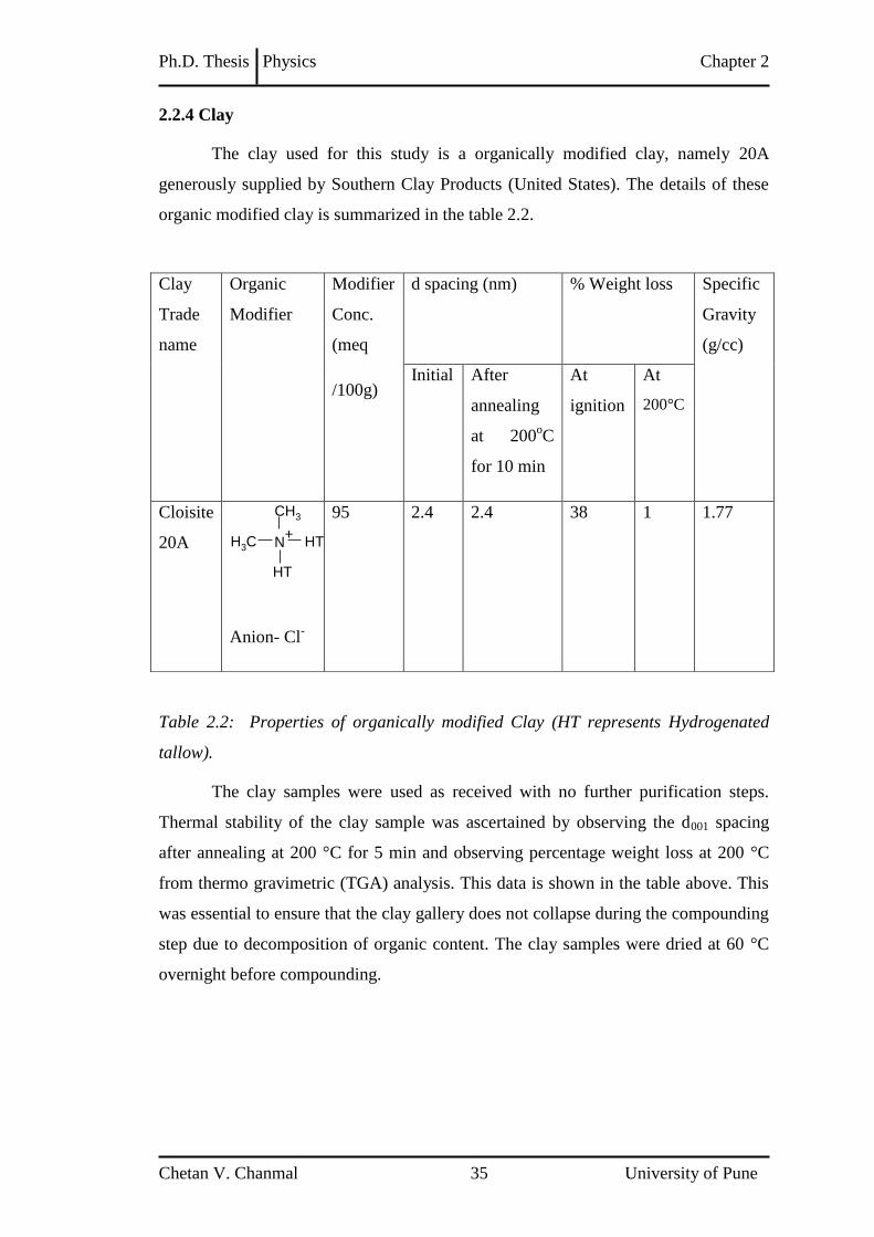
Ph.D. Thesis Physics Chapter 2
Chetan V. Chanmal 35 University of Pune
2.2.4 Clay
The clay used for this study is a organically modified clay, namely 20A
generously supplied by Southern Clay Products (United States). The details of these
organic modified clay is summarized in the table 2.2.
Table 2.2: Properties of organically modified Clay (HT represents Hydrogenated
tallow).
The clay samples were used as received with no further purification steps.
Thermal stability of the clay sample was ascertained by observing the d001 spacing
after annealing at 200 °C for 5 min and observing percentage weight loss at 200 °C
from thermo gravimetric (TGA) analysis. This data is shown in the table above. This
was essential to ensure that the clay gallery does not collapse during the compounding
step due to decomposition of organic content. The clay samples were dried at 60 °C
overnight before compounding.
Clay
Trade
name
Organic
Modifier
Modifier
Conc.
(meq
/100g)
d spacing (nm) % Weight loss
Specific
Gravity
(g/cc)
Initial After
annealing
at 200oC
for 10 min
At
ignition
At
200°C
Cloisite
20A NH3C
HT
HT
CH3
+
Anion- Cl-
95 2.4 2.4 38 1 1.77

Ph.D. Thesis Physics Chapter 2
Chetan V. Chanmal 36 University of Pune
2.3 Fabrication of Nanocomposites
2.3.1 Melt Compounding Technique
The nanocomposites are prepared using melt compounding technique. A
Haake Polylab batch mixer having 50 gm capacity is used for the compounding of
nanocomposites of MWCNT and BaTiO3 nanoparticles. The batch mixer is a
Rheomix 600P equipped with roller rotors R600. The melt compounding is carried
out at 200 °C for 5 min at a rotor speed of 60 rpm.
The films for different characterization were prepared by compression
molding using Carver press model F-15181. An appropriate quantity of material is
taken and heated above melting temperature between metal sheets, which are sprayed
using mold release spray. Nominal pressure is applied to get the required thickness of
the film. Platens of carver press are then cooled using water circulation. These films
are used for further characterization.
2.3.2 Pulsed Laser Deposition (PLD)
Pulsed Laser Deposition is a physical vapor deposition method, carried out in
a vacuum chamber. The experimental setup consists of a high energy laser source
(generally an UV excimer laser like KrF (248 nm), ArF (193 nm) or Nd: YAG laser)
and a vacuum chamber (capable of evacuating in the order of ~10-6
mbar with the help
of rotary and turbo molecular pumps). The vacuum chamber is equipped with a
rotating target holder (where multiple target mounting is possible for the multilayer
deposition) controlled by a motor and a substrate holder, which can be simultaneously
heated with the help of a heater controlled by a thermocouple. A gas inlet for inserting
reacting gases, such as oxygen is also provided. The laser beam incident at an angle of
45° to the target surface is focused on to the rotating target (made up of the material to
be deposited) with a quartz lens. Laser beam of energy ~100 to 400 mJ is focused to a
size such that energy density is maintained between 1 to 5 J/cm2, at the target. The
deposition processes can be controlled by externally connected computer. For the
deposition, at sufficiently high laser energy, the target material is ablated to form
plasma plume. The plasma plume contains various excited atoms, molecules, ions and
small particles. This plasma quickly expands away from the target towards the
substrate where it is deposited at the surface of the heated substrate leading to growth
of the desired thin film.
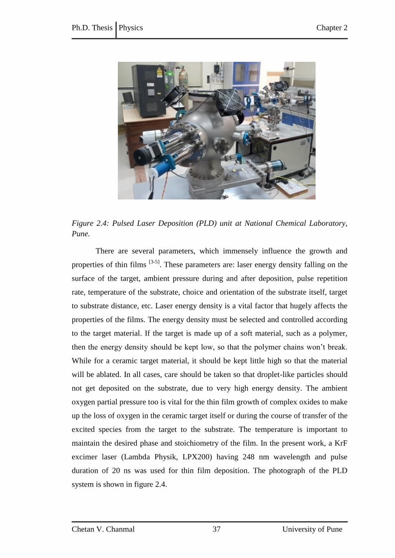
Ph.D. Thesis Physics Chapter 2
Chetan V. Chanmal 37 University of Pune
Figure 2.4: Pulsed Laser Deposition (PLD) unit at National Chemical Laboratory,
Pune.
There are several parameters, which immensely influence the growth and
properties of thin films [3-5]
. These parameters are: laser energy density falling on the
surface of the target, ambient pressure during and after deposition, pulse repetition
rate, temperature of the substrate, choice and orientation of the substrate itself, target
to substrate distance, etc. Laser energy density is a vital factor that hugely affects the
properties of the films. The energy density must be selected and controlled according
to the target material. If the target is made up of a soft material, such as a polymer,
then the energy density should be kept low, so that the polymer chains won’t break.
While for a ceramic target material, it should be kept little high so that the material
will be ablated. In all cases, care should be taken so that droplet-like particles should
not get deposited on the substrate, due to very high energy density. The ambient
oxygen partial pressure too is vital for the thin film growth of complex oxides to make
up the loss of oxygen in the ceramic target itself or during the course of transfer of the
excited species from the target to the substrate. The temperature is important to
maintain the desired phase and stoichiometry of the film. In the present work, a KrF
excimer laser (Lambda Physik, LPX200) having 248 nm wavelength and pulse
duration of 20 ns was used for thin film deposition. The photograph of the PLD
system is shown in figure 2.4.

Ph.D. Thesis Physics Chapter 2
Chetan V. Chanmal 38 University of Pune
2.3.3 Electrospinning
Electrospinning is a simple and versatile process by which polymer fibers with
diameter ranging from few nanometers to several micrometers can be produced from
a rich variety of materials that include polymers, composites and ceramics. The fibers
produced possess extraordinary unique characteristics such as high surface area per
unit mass coupled with remarkable high porosity, excellent structural mechanical
properties [6, 7]
. Electrospinning technique is found to be unique and cost effective
route for fabricating fibers for a variety of applications. Choice of polymer solution
and control on processing parameters provide a capacity of nanofibers produced with
the range of diverse properties. The rheological properties of polymer solution or melt
are enhanced, sometimes using external additives, to improve the efficiency of the
electrospinning process.
Figure 2.5: Schematic of electrospinning setup.
In a typical electrospinning process, a high electrical potential is applied
between droplet of a polymer solution, or melt, held at the capillary tube and a
grounded collector. When the applied electrostatic force overcomes the surface
tension of the droplet, a charged jet of polymer solution is ejected. The route of the
charged jet is controlled by electric field. The charged jet travels linearly for only a
short distance before undergoing bending instability, resulting in the formation of
looping trajectory of the jet. The electrospinning process is shown in figure 2.5.
Dependence of process parameters & solution parameters:
The following process variables and solution parameters affect the
electrospinning process
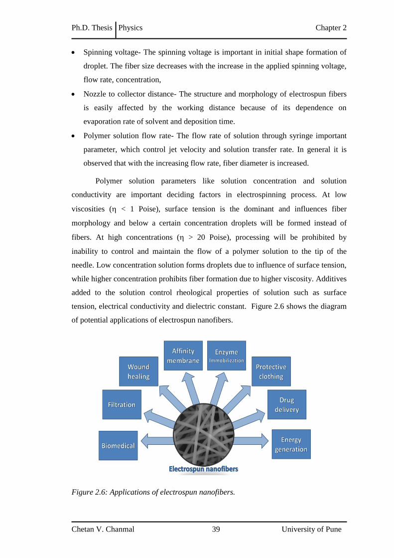
Ph.D. Thesis Physics Chapter 2
Chetan V. Chanmal 39 University of Pune
Spinning voltage- The spinning voltage is important in initial shape formation of
droplet. The fiber size decreases with the increase in the applied spinning voltage,
flow rate, concentration,
Nozzle to collector distance- The structure and morphology of electrospun fibers
is easily affected by the working distance because of its dependence on
evaporation rate of solvent and deposition time.
Polymer solution flow rate- The flow rate of solution through syringe important
parameter, which control jet velocity and solution transfer rate. In general it is
observed that with the increasing flow rate, fiber diameter is increased.
Polymer solution parameters like solution concentration and solution
conductivity are important deciding factors in electrospinning process. At low
viscosities ( < 1 Poise), surface tension is the dominant and influences fiber
morphology and below a certain concentration droplets will be formed instead of
fibers. At high concentrations ( > 20 Poise), processing will be prohibited by
inability to control and maintain the flow of a polymer solution to the tip of the
needle. Low concentration solution forms droplets due to influence of surface tension,
while higher concentration prohibits fiber formation due to higher viscosity. Additives
added to the solution control rheological properties of solution such as surface
tension, electrical conductivity and dielectric constant. Figure 2.6 shows the diagram
of potential applications of electrospun nanofibers.
Figure 2.6: Applications of electrospun nanofibers.

Ph.D. Thesis Physics Chapter 2
Chetan V. Chanmal 40 University of Pune
2.3.4 Spin Coating
Spin coating is a widely used technique in the semiconductor industry for the
deposition of polymer resist layers. A requirement for this technique is a good
solubility of the polymer. Typical, spin coating procedure involves deposition of a
small amount of a solution onto the centre of a substrate as shown in Figure 2.7,
which is then spun around at a high speed so that the solution is spread out by the
centrifugal force. The centrifugal force causes the excess solution to fly off the
substrate and simultaneously, some of the solvent evaporates. The evaporation
process raises the concentration and viscosity of the remaining solution. This high
viscosity prevents the solution from exiting the substrate and a thin film of solution
remains. Continued spinning evaporates the rest of the solvent after which a thin film
of polymer is obtained. The spinning speed ranges from 1000 to 3500 rpm, depending
on the interest of the film thickness. In a programmable spin coater, the solution is
first spin coated at slower rate (of 100 rpm) so that the solution fully covers the
substrate. Then a high speed is selected depending on the required film thickness.
Final film thickness and other properties depend on the nature of the resin (viscosity,
drying rate, percent solids, surface tension etc.) and the parameters chosen for the spin
process. Factors such as final rotational speed, acceleration, and fume exhaust
contribute to how the properties of coated films are defined.
Some variable process parameters involved in spin coating are:
Solution viscosity
Solid content
Angular speed
Spin Time
Figure 2.7: Illustration of Spin Coating.

Ph.D. Thesis Physics Chapter 2
Chetan V. Chanmal 41 University of Pune
2.4 Characterization Techniques
2.4.1 X-ray Diffraction (XRD)
X-ray diffraction (XRD) is a non–destructive analytical characterization
technique for identification and quantitative determination of long–range order in
various crystalline compounds [9, 10]
. Crystal structure can be studied through
diffraction pattern of waves that interact with atoms and have wavelength comparable
with interatomic spacing in crystals. This technique is suitable for thin films, bulk and
nanomaterials [11].
The basic components of the instrument are X - ray tube (X-ray generator),
goniometer, detector, and the software. When fast moving electrons collide with the
target atoms a continuous spectrum of X-ray is emitted known as Bremsstrahlung
radiations. If the accelerating voltage is sufficient enough characteristic X-ray of
target are produced. Copper and Molybdenum are commonly used targets that emit
characteristic X - rays of wavelength 0.154 nm and 0.08 nm respectively. The energy
of an X-ray photon is related to its wavelength and is given by [12]
:
Where h is Planck’s constant, is the frequency, c is the velocity of light, is energy
of the photon and is the wavelength of X-ray source. Crystal studies require photon
energies in the 10 to 50 KeV range.
The working principle of XRD can be understood from Bragg’s law. Consider
a collimated parallel beam of X-rays is incident on the sample as shown in figure 2.8.
The diffracted beams are found when the reflections from parallel planes of the atoms
interfere constructively. Let the parallel lattice planes in crystal are spaced at a
distance d apart. Constructive interference of the irradiation from successive planes
occurs when path difference is an integral multiple (n) of wavelength . Therefore,
This is the Braggs law.
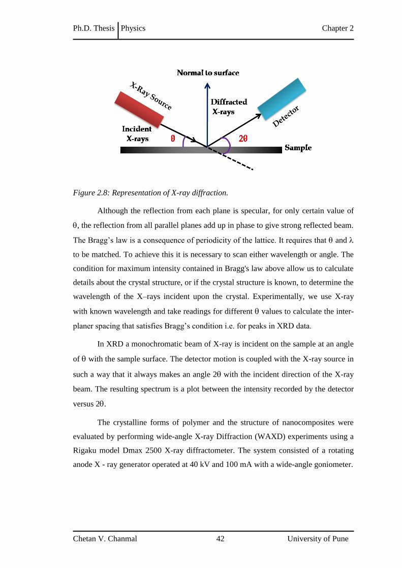
Ph.D. Thesis Physics Chapter 2
Chetan V. Chanmal 42 University of Pune
Figure 2.8: Representation of X-ray diffraction.
Although the reflection from each plane is specular, for only certain value of
, the reflection from all parallel planes add up in phase to give strong reflected beam.
The Bragg’s law is a consequence of periodicity of the lattice. It requires that and
to be matched. To achieve this it is necessary to scan either wavelength or angle. The
condition for maximum intensity contained in Bragg's law above allow us to calculate
details about the crystal structure, or if the crystal structure is known, to determine the
wavelength of the X–rays incident upon the crystal. Experimentally, we use X-ray
with known wavelength and take readings for different values to calculate the inter-
planer spacing that satisfies Bragg’s condition i.e. for peaks in XRD data.
In XRD a monochromatic beam of X-ray is incident on the sample at an angle
of with the sample surface. The detector motion is coupled with the X-ray source in
such a way that it always makes an angle 2with the incident direction of the X-ray
beam. The resulting spectrum is a plot between the intensity recorded by the detector
versus 2.
The crystalline forms of polymer and the structure of nanocomposites were
evaluated by performing wide-angle X-ray Diffraction (WAXD) experiments using a
Rigaku model Dmax 2500 X-ray diffractometer. The system consisted of a rotating
anode X - ray generator operated at 40 kV and 100 mA with a wide-angle goniometer.
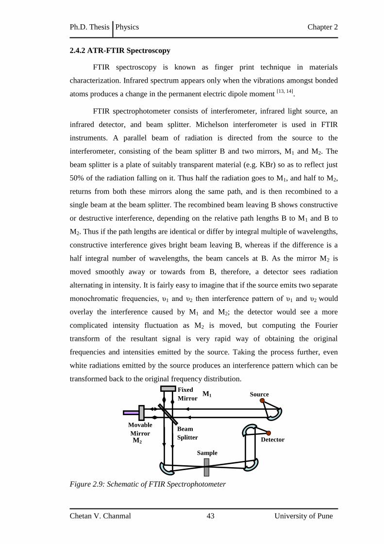
Ph.D. Thesis Physics Chapter 2
Chetan V. Chanmal 43 University of Pune
2.4.2 ATR-FTIR Spectroscopy
FTIR spectroscopy is known as finger print technique in materials
characterization. Infrared spectrum appears only when the vibrations amongst bonded
atoms produces a change in the permanent electric dipole moment [13, 14]
.
FTIR spectrophotometer consists of interferometer, infrared light source, an
infrared detector, and beam splitter. Michelson interferometer is used in FTIR
instruments. A parallel beam of radiation is directed from the source to the
interferometer, consisting of the beam splitter B and two mirrors, M1 and M2. The
beam splitter is a plate of suitably transparent material (e.g. KBr) so as to reflect just
50% of the radiation falling on it. Thus half the radiation goes to M1, and half to M2,
returns from both these mirrors along the same path, and is then recombined to a
single beam at the beam splitter. The recombined beam leaving B shows constructive
or destructive interference, depending on the relative path lengths B to M1 and B to
M2. Thus if the path lengths are identical or differ by integral multiple of wavelengths,
constructive interference gives bright beam leaving B, whereas if the difference is a
half integral number of wavelengths, the beam cancels at B. As the mirror M2 is
moved smoothly away or towards from B, therefore, a detector sees radiation
alternating in intensity. It is fairly easy to imagine that if the source emits two separate
monochromatic frequencies, υ1 and υ2 then interference pattern of υ1 and υ2 would
overlay the interference caused by M1 and M2; the detector would see a more
complicated intensity fluctuation as M2 is moved, but computing the Fourier
transform of the resultant signal is very rapid way of obtaining the original
frequencies and intensities emitted by the source. Taking the process further, even
white radiations emitted by the source produces an interference pattern which can be
transformed back to the original frequency distribution.
Figure 2.9: Schematic of FTIR Spectrophotometer
Beam
Splitter
Sample
Detector
Source Fixed
Mirror
Movable
Mirror
M1
M2

Ph.D. Thesis Physics Chapter 2
Chetan V. Chanmal 44 University of Pune
Attenuated total reflectance (ATR) is a sampling technique used in
conjunction with infrared spectroscopy which enables samples to be examined
directly in the solid or liquid state without further preparation. Light undergoes
multiple internal reflections in the crystal of high refractive index, shown in blue. The
sample is in contact with the crystal.
Figure 2.10: Schematic of working of ATR-FTIR spectroscopy.
ATR uses a property of total internal reflection resulting in an evanescent
wave. A beam of infrared light is passed through the crystal of high refractive index
such as ZnSe. Radiation from source enters the crystal where it undergoes series of
total internal reflections before exiting crystal. This reflection forms the evanescent
wave which extends into the sample. The penetration depth into the sample is
typically between 0.5 and 2 micrometers, with the exact value being determined by
the wavelength of light, the angle of incidence and the indices of refraction for the
ATR crystal and the medium being probed. The beam is then collected by a detector
as it exits the crystal. This evanescent effect only works if the crystal is made of an
optical material with a higher refractive index than the sample being studied. In the
case of a solid sample, it is pressed into direct contact with the crystal. The result is a
selective attenuation of the radiation at those wavelengths at which the sample
absorbs. Because the evanescent wave into the solid sample is improved with a more
intimate contact, solid samples are usually firmly clamped against the ATR crystal, so
that trapped air is not the medium through which the evanescent wave travels, as that
would distort the results.
ATR-IR data presented in the thesis were taken from Perkin-Elmer FTIR
Spectrum one spectrophotometer operated at a resolution of 4 cm-1
. Ten spectra were
recorded for averaging.
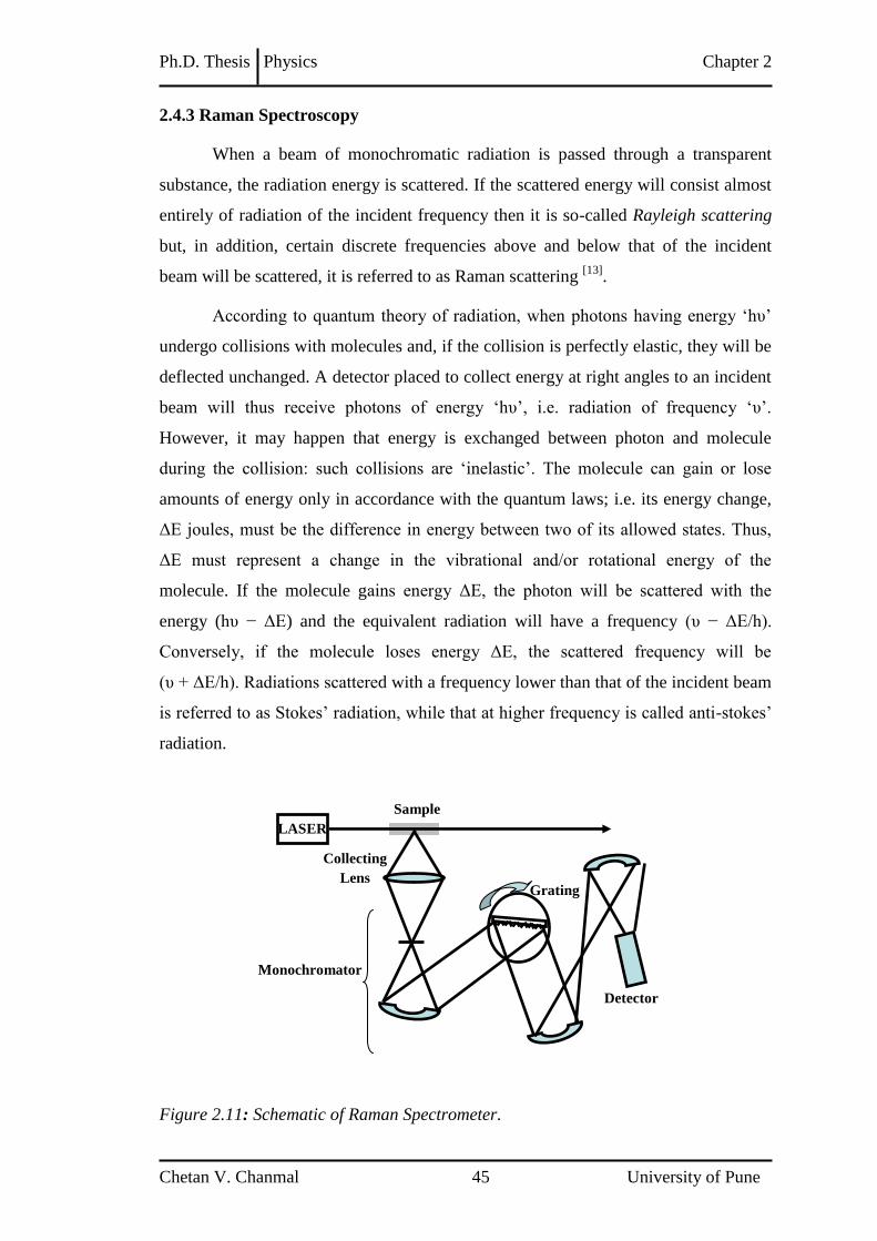
Ph.D. Thesis Physics Chapter 2
Chetan V. Chanmal 45 University of Pune
2.4.3 Raman Spectroscopy
When a beam of monochromatic radiation is passed through a transparent
substance, the radiation energy is scattered. If the scattered energy will consist almost
entirely of radiation of the incident frequency then it is so-called Rayleigh scattering
but, in addition, certain discrete frequencies above and below that of the incident
beam will be scattered, it is referred to as Raman scattering [13]
.
According to quantum theory of radiation, when photons having energy ‘hυ’
undergo collisions with molecules and, if the collision is perfectly elastic, they will be
deflected unchanged. A detector placed to collect energy at right angles to an incident
beam will thus receive photons of energy ‘hυ’, i.e. radiation of frequency ‘υ’.
However, it may happen that energy is exchanged between photon and molecule
during the collision: such collisions are ‘inelastic’. The molecule can gain or lose
amounts of energy only in accordance with the quantum laws; i.e. its energy change,
ΔE joules, must be the difference in energy between two of its allowed states. Thus,
ΔE must represent a change in the vibrational and/or rotational energy of the
molecule. If the molecule gains energy ΔE, the photon will be scattered with the
energy (hυ − ΔE) and the equivalent radiation will have a frequency (υ − ΔE/h).
Conversely, if the molecule loses energy ΔE, the scattered frequency will be
(υ + ΔE/h). Radiations scattered with a frequency lower than that of the incident beam
is referred to as Stokes’ radiation, while that at higher frequency is called anti-stokes’
radiation.
Figure 2.11: Schematic of Raman Spectrometer.
LASER
Collecting
Lens
Detector
Sample
Cell
Grating
Monochromator
Ph.D. Thesis Physics Chapter 2
Chetan V. Chanmal 46 University of Pune
Figure 2.11 shows the schematic of Raman spectrometer. Raman Spectrometer
consists of Laser beam (very narrow, monochromatic, coherent and powerful) which
when passed through the sample cell (usually a narrow glass or quartz tube filled with
the sample) get scattered sideways from the sample, which is collected by a lens and
passed into a grating monochromator. The signal is measured by a sensitive photo
multiplier tube (PMT) and after amplification; it is usually processed by a computer
which plots the Raman spectrum.
Raman spectroscopy measurements were done on confocal micro-Raman
spectrometer LabRAM ARAMIS Horiba Jobin-Yvon apparatus with laser excitation
wavelength of 632 nm.
2.4.4 Scanning Electron Microscopy (SEM)
Scanning Electron Microscopy allows direct observations of topography and
morphological features with high resolution and depth of field than optical
microscope. In SEM electron beam is focused onto surface of the specimen and
scanned back and forth across the surface [15, 16]
.
A typical schematic of a SEM is shown in figure 2.12. The instrument can be
simplified into three major sections: a) electron-optical column; b) vacuum system
and c) electronics and display system. The electron column consists of an electron gun
and two or more electron lenses, which influence the path of electrons travelling down
an evacuated tube.
A tungsten filament is heated to 2700 K, which produces electrons that are
accelerated at the voltages in the range of 2 to 40 kV. Condenser lens system is used
to focus the electron beam to a diameter of about 5 nm. Ultimate performance of the
SEM is mainly limited by the diameter of the beam. The surface of the specimen is
brought into the focus of electron beam. These fast primary electrons (PE) interact in
various ways with the surface layers of the specimen. A cathode-ray display tube is
scanned synchronously with the electron beam. The signals produced control the
brightness of a screen tube such that an image of the surface of the sample appears.
The samples should be electrically conductive, otherwise, it may get overcharged due
to the irradiations.

Ph.D. Thesis Physics Chapter 2
Chetan V. Chanmal 47 University of Pune
Figure 2.12: Schematic diagram of Scanning Electron Microscope (SEM).
[http://www.rpi.edu/dept/materials/COURSES/NANO/shaw/Page5.html]
When the electron beam interacts with the specimen, many types of signals are
generated. The two signals most often used to produce SEM images are secondary
electrons (SE) and backscattered electrons (BSE). These elastically scattered electrons
usually called 'backscattered electrons' (BSE) are used for backscattered electron
imaging. These images provide information about the distribution of different
elements in the sample as the intensity of backscattered electrons strongly depends on
the atomic number (Z) of the elements in the sample. Some other electrons scatter
inelastically due to the loss in kinetic energy upon their interaction with orbital shell
electrons. The incident electrons may knock off loosely bound conduction electrons
out of the surface of the sample. These are secondary electrons (SE) and are used for
SEM topographical imaging.

Ph.D. Thesis Physics Chapter 2
Chetan V. Chanmal 48 University of Pune
2.4.5 Transmission Electron Microscopy (TEM)
TEM operates on the same basic principles as that of light microscope but uses
electrons instead of light. What we can see with a light microscope is limited by the
wavelength of light. TEM uses electrons as "light source" and their much lower
wavelength makes it possible to get a resolution thousand times better than that with a
light microscope [17]
. We can see objects to the order of a few nanometers (10-9
m).
The basic components of TEM are: an electron optical column, a vacuum
system, necessary electronics (lens supplies for focusing and deflecting the beam and
the high voltage generator for the electron source) and the software. In TEM, a thin
specimen is illuminated with uniform and high intensity electrons. The interaction of
an electron beam with a solid specimen results in a number of elastic or inelastic
scattering phenomena. In this thin area, only a few electrons are scattered and more
than 90% of the incident beam is undeviated. Regions of the specimen, which are
thicker, or of higher density will scatter the electron beam more strongly and will
appear darker in the image. If the specimen is too thick, the number of electrons
transmitted reduces and this reduces the contrast. Hence, the specimen thickness
should be of the order of 100 nm or less.
Figure 2.13: Schematic diagram of the Transmission Electron Microscope (TEM).
[http://www.rpi.edu/dept/materials/COURSES/NANO/shaw/Page5.html]

Ph.D. Thesis Physics Chapter 2
Chetan V. Chanmal 49 University of Pune
2.4.6 Dielectric Relaxation Spectroscopy (DRS)
The dielectric relaxation spectroscopy (DRS) has been emerged as a powerful
technique in probing the relaxation dynamics of polymer matrix at molecular level
[18, 19]. The major advantage of using dielectric spectroscopy compared to other
techniques is the broad frequency range covered in this technique. The broad
frequency range allows investigating different characteristic relaxation processes
having wide range of time and length scales. In dielectric spectroscopy, by observing
the dipolar relaxation as a function of temperature and frequency, effects due to
intermolecular co-operative segmental motion and hindered dipole orientation can be
elucidated.
A typical set up for the measurement dielectric properties is shown in
figure 2.14. Dielectric properties of the samples in the film phase are measured using
the Novo Control Alpha A Analyzer equipped with ZGS active sample cell having
temperature controller and WinDeta, WinImp and WinFit softwares. The samples are
scanned between frequencies 0.01Hz and 1MHz at temperature ranging from 30 to
100 °C. Bias voltage applied across the sample is 0.1 V. The electrode of 20 mm
diameter is used while thickness of the sample is measured and used while calculating
the dielectric constant.
Figure 2.14: Schematic of principle of dielectric spectroscopy.
In dielectric spectroscopy, a small electric perturbation in the form of
sinusoidal voltage is applied to samples. The electric field produces polarization,
causing oscillation of the same frequency as that of the applied field but with a phase
shift (). The phase angle shift is measured by comparing the applied voltage to the
measured current. The measured response is represented into a complex form (*) that

Ph.D. Thesis Physics Chapter 2
Chetan V. Chanmal 50 University of Pune
can be separated into capacitive and conductive components giving the real part of
permittivity (′) and loss factor (").
The complex permittivity is defined as:
Where, ′ is the real part of permittivity and ″ is the imaginary part of permittivity.
The ratio of the imaginary to the real part (″/′) is termed as ‘‘dissipation factor’’
which is represented by tan , where is the phase angle between applied voltage and
resulting current
The various relaxation processes with different time scales and length scales
can be studied using dielectric spectroscopy. Following are the characteristic
relaxation processes seen in polymer nanocomposites as a function of frequency and
temperature,
Co-operative relaxation (a) - Co-operative segmental relaxation in the
amorphous phase of polymer associated with the onset of glass transition
temperature (Tg).
Crystalline relaxation (c) - Relaxation in local crystalline chains of polymer.
Maxwell-Wagner-Sillars (MWS) polarization - MWS polarization is
associated with the charge trapping at the interface of composites having
materials with large difference in the permittivity.
Fitting to Experimental Data
Frequency dependent dielectric permittivity can be studied using several
models. Debye was the first to predict the frequency dependence of dielectric
relaxations in polymers [18]
.
The Debye equation for fitting the dielectric spectra is given by:
Where s−∞is relaxation strength (s is low frequency permittivity and ∞is
high frequency permittivity), relaxation time, = 2f.

Ph.D. Thesis Physics Chapter 2
Chetan V. Chanmal 51 University of Pune
Generally the relaxation time distribution in polymers is much broader and
asymmetric than a single Debye process. A phenomenological model which accounts
for the broader and asymmetric nature of the relaxation was developed by Havriliak-
Negami (H-N) based on empirical modification to Debye equation [20, 21]
. The H-N
equation also takes into consideration the dc conductivity contribution and is given by
following equation:
Where dc = dc conductivity, & are the shape parameters describing the
symmetric and asymmetric broadening parameters respectively, relaxation time,
s−∞is relaxation strength and = 2f.
H-N equation is the generalized equation for fitting the dielectric relaxation of
polymer as it also includes Cole-Cole equation ( =1), Cole-Davidson equation (=1)
and Debye equation (==1) as a special case. H-N analysis provides better
understanding of the relaxation time scale ( ), the magnitude (relaxation strength) and
the shape (, ) of each relaxation processes; particularly, time scale of relaxation
processes that can be extracted from the H-N equation fitting. This relaxation time can
be further analyzed in terms of Arrhenius equation for determining the activation
energy of the relaxation process.
Activation energy:
The temperature dependence of a relaxation process can be analyzed by
plotting the frequency maximum against the reciprocal temperature. The maximum
frequency (or temperature) of the peak in the loss spectrum is related to the mean
relaxation time of the process and characterizes the molecular mobility.
The crystalline relaxation and MWS relaxation are known to follow Arrhenius
type equation given by following equation [22]
:
Where fmax = Frequency maximum in permittivity loss spectra, Ea = Activation
energy, K is the Boltzmann’s constant, and T is the temperature.

Ph.D. Thesis Physics Chapter 2
Chetan V. Chanmal 52 University of Pune
Unlike the crystalline and MWS relaxation, the time- temperature relationship
of the segmental relaxation corresponding to glass transition temperature normally
follows a non-linear behavior and can be described by the Vogel-Fulcher-Tammann
(VFT) equation given by:
Where related inversely with frequency, is the segmental relaxation time and is
the prefactor correlated to the time scale at which the molecules are attempting to
overcome some energy barrier. B is a parameter related to the strength for glass-
forming. T0 is a temperature below Tg and at which the segments would be frozen if
they were at equilibrium. The width and the asymmetry associated with the
distribution of the relaxation times result from a local structural heterogeneity.
Modulus Formalism:
The electric modulus formalism was introduced by McCrum et al. [23]
and it is
used to study electrical relaxation phenomena in many polymers [24-25]
. According to
its definition, variations in the large values of permittivity and conductivity at low
frequencies are minimized and hence common difficulties like electrode nature and
contact, space charge injection phenomena and absorbed impurity conduction effects
can be resolved. Electric modulus is an electrical analogue to the mechanical shear
modulus.
Electric modulus is defined as a quantity inversely proportional to permittivity
and is given by the following equation:
Where M′ and M″ are the real and the imaginary part of electric modulus respectively
and ε′ and ε″ are the real and the imaginary part of dielectric permittivity. The electric
modulus formalism has unique advantages in the interpretation of slow relaxation
phenomena processes like MWS relaxation.

Ph.D. Thesis Physics Chapter 2
Chetan V. Chanmal 53 University of Pune
To elucidate the importance of electric modulus, we present the dielectric
relaxation spectra of PVDF in permittivity and electric modulus formalism shown in
Figure 2.15. The dielectric permittivity (ε″) curve for PVDF shows single relaxations
at around 10+04
Hz and is attributed to crystalline chain relaxation in PVDF. However
when the same data is presented in modulus presentation, two relaxations are clearly
discernible. An additional peak (around 10+00
Hz) in the low frequency region appears
in modulus presentation, which was completely masked in permittivity spectra in the
low frequency region. This low frequency relaxation is identified as Maxwell-
Wagner-Sillars (MWS) relaxation and is observed in many crystalline polymers. This
MWS relaxation is attributed to the trapping of ionic charges at the interface between
the amorphous and the crystalline regions of the polymer.
Figure 2.15: Dielectric relaxation spectra of PVDF in permittivity and modulus
formalism.

Ph.D. Thesis Physics Chapter 2
Chetan V. Chanmal 54 University of Pune
2.4.7 Ferroelectric Analysis
Ferroelectricity is a property of certain materials which possess a spontaneous
electric polarization that can be reversed by the application of an external electric
field. The term is used in analogy to ferromagnetism, in which a material exhibits a
permanent magnetic moment. Ferromagnetism was already known when
ferroelectricity was discovered in 1920 in Rochelle salt by Valasek. The
distinguishing feature of ferroelectrics is that the direction of the spontaneous
polarization can be reversed by an applied electric field, yielding a hysteresis loop.
The word spontaneous may mean that the polarization has non-zero value in the
absence of electric field. The measurement of hysteresis loop is carried out by
applying a sinusoidal voltage to the sample and polarization reversal current and/ or
charge is continuously monitored. These measurements allow the determination of
remnant polarization (amount of polarization after the poling field has been removed)
and the coercive field which are the characteristic features of the ferroelectric
materials.
Figure 2.16: The Sawyer-Tower circuit to measure the polarization-electric field
characterization.
The Sawyer-tower method is the simplest method to measure the polarization.
As shown in figure 2.16 here the ferroelectric capacitor C is kept parallel to a standard
capacitor C0. A sinusoidal voltage signal is applied to one of the electrodes of the
ferroelectric capacitor and the amount of charge displacement in the other electrode is

Ph.D. Thesis Physics Chapter 2
Chetan V. Chanmal 55 University of Pune
measured using the voltage it creates over a reference capacitor connected in series.
The voltage V sufficient to polarize the ferroelectric material
Where, A is the capacitor area, P is the polarization, V is applied ac voltage of
low frequency with the applied field across the specimen as
, with d
as the sample thickness. Ferroelectricity analysis was carried out using aixACCT
systems, GmbH Germany at ARDE, Pune.
2.5 References
1. Hyun-Wook Lee, San Moon, Chang-Hak Choi, Do Kyung Kim, J. Am. Ceram.
Soc., 2012, 1-6.
2. L. Bokobza, J. Zhang, eXPRESS Polymer Letters, 2012, 6,601–608.
3. “Pulsed Laser Deposition of Thin Films: Applications-Led Growth of
Functional Materials”, edited by Robert Eason, Wiley-Interscience A John
Wiley & Sons, Inc., Publication, Hoboken, New Jersey, 2007
4. M S Hegde, Proc. Indian Acad. Sci. (Chem. Sci.), 2001, 113, 445–458.
5. “Pulsed Laser Deposition of Thin Films”, edited by D. B. Chrisey, G. H.
Hubler, Wiley Interscience Publication, NewYork, 1994.
6. Katarzyna M. Sawicka , Perena Gouma, Journal of Nanoparticle Research
2006, 8, 769–781
7. Wu Aik Yee , Masaya Kotaki , Ye Liu , Xuehong Lu, Polymer, 2007, 48, 512-
521.
8. David B. Hall, Patrick Underhill, John M. Torkelso, Polymer Engineering And
Science, 1998, 38, 2040.
9. D. Dijkamp, T. Venkatesan, X. D. Wu, S. A. Shaheen, N. Jisrawi, Y. H. Min-
Lee, W. L. McLean, M. Croft, Appl. Phys. Lett., 1987, 51, 619.
10. X. D. Wu, D. Dijkamp, S. B. Ogale, A. Inam, E. W. Chase, P. F. Miceli, C. C.
Chang, J. M. Tarascon, T. Venkateshan Appl. Phys. Lett., 1987, 51, 861.
11. Elements of X-ray Diffraction, ed. by B. D. Cullity, Addison Wesley Publishing
Co., 1978.

Ph.D. Thesis Physics Chapter 2
Chetan V. Chanmal 56 University of Pune
12. R. W. G. Wyckoff, Crystal Structures, 2nd ed., Wiley, New York, 1964
13. C. N. Banwell, E. M. McCash, Fundamentals of Molecular Spectroscopy, 4th
Ed., Tata McGraw Hill Publishing Co. Ltd., 2002.
14. J. Coates, Interpretation of Infrared Spectra: A Practical Approach,
Encyclopedia of Analytical Chemistry, R.A. Meyers (Ed.), 10815, John Wiley &
Sons Ltd, 2000.
15. G. Lawes, “Scanning electron microscopy and X-ray microanalysis: Analytical
chemistry by open learning”, John Wiley & Sons, 1987.
16. Jonathan Atteberry, "How Scanning Electron Microscopes Work" 21 April
2009.HowStuffWorks.com http://science.howstuffworks.com/scanningelectron-
microscope.htm> 13 September 2013.
17. "Transmission electron microscope". Art. Encyclopedia Britannica Online.
Web. 13 Sep.
18. H. Hammamia, M. Arous, M. Lagache, A. Kallel, Journal of Alloys and
Compounds, 2007, 430, 1-8.
19. F. Kremer, Journal of Non-Crystalline Solids, 2002, 30, 1-9.
20. A. Kyritsis, G. Vikelis, P. Maroulas, P. Pissis, B. Milosheva, R. Kotsilkova, A.
Toplijska, C. Silvestre, D. Duraccio, Journal of Applied Polymer Science, 2011,
121, 3613-3627.
21. A.C. Comer, A.L. Heilman, D.S. Kalika, Polymer, 2010, 51, 5245-5254.
22. S.A. Madbouly, J.U. Otaigbe, Polymer, 2007, 48, 4097-4107.
23. McCrum, N. G., Read, B. E., Williams G., Anelastic and dielectric effects in
polymeric solids, Wiley, London, 1967.
24. G.C. Psarrasas, E. Manolakakib, G.M. Tsangaris, Composites: Part A, 2003, 34,
1187–1198.
25. M. Arous, I.B. Amor, A. Kallel, Z. Fakhfakh, G. Perrier, Journal of Physics and
Chemistry of Solids, 2007, 68, 1405-1414.

Chetan V. Chanmal 57 University of Pune
Chapter 3
Dielectric Relaxations and Low Thermal
Emissivity Studies of PVDF/BaTiO3
Nanocomposites
In this chapter we describe the fabrication and dielectric relaxation studies of
PVDF/BaTiO3 nanocomposites. The nanocomposites exhibit enhanced dielectric
permittivity with relatively low dielectric losses. The dielectric relaxation dynamics of
nanocomposites was studied in details using different formalisms. The analysis
showed presence of different dielectric relaxations which are attributed to crystalline
(c), glass transition (a), and Maxwell-Wagner-Sillars (MWS) relaxations. The
nanofibers of PVDF/BaTiO3 were prepared by electrospinning technique. The
PVDF/BaTiO3 nanofibers were found to crystallize in ferroelectric phase during
electrospinning process. The electrospun fibers were tested for low thermal emissivity
material having application in camouflaging technology. The nanocomposite
nanofibers showed reduction in the thermal emissivity.
Part of the work presented in this chapter has been published in following
journals:
1. C.V. Chanmal, J. P. Jog, eXpress Polymer letters, 2008, 2, 294-301.
2. C. V. Chanmal, J. P. Jog, Int. J. Plast. Technology, 2011.

Ph.D. Thesis Physics Chapter 3
Chetan V. Chanmal 58 University of Pune
Section I: Dielectric Relaxation Dynamics in PVDF/BaTiO3 Nanocomposites
3.I.1 Introduction
Polymer loaded with electroactive ceramics have been studied extensively
because of the need for flexible materials having high dielectric permittivity and low
processing cost [1]
. In these nanocomposites, the final properties depend essentially
on many parameters such as grain size of ceramic, preparation method of composites
and on the dispersion of the ceramic particles into the polymer matrix [2, 3, 4, 5]
.
PVDF is a semicrystalline polymer and exhibits different polymorphic phases.
PVDF has relatively high dielectric permittivity and low dissipation factor making it a
suitable material for many applications [6, 7]
. PVDF is also studied extensively in
industrial applications for its piezoelectric and pyroelectric properties. Generally,
piezoelectricity in polymers has an advantage over piezoelectric ceramics for certain
applications wherein acoustic impedance similar to that of water or living tissue is
required [8]
. Due to excellent electrical properties and semicrystalline structure, the
investigation of dielectric and electrical behaviors of PVDF is essential from the
fundamental and technological point of view [9]
.
Pure polymers have low dielectric permittivity, even though they have high
dielectric breakdown strength. In many applications it is essential to have material
having high dielectric permittivity with low dissipation factor. One common approach
to increase the dielectric permittivity of polymer is to add ferroelectric ceramic into
the polymer matrix. In last decade, significant efforts were made to combine the
ferroelectric properties of polymer and high dielectric permittivity of the ceramic
material. These nanocomposites can be potential material for high breakdown
strength, charge storage and high dielectric permittivity applications. Although there
are few reports on the studies of dielectric properties of PVDF/BaTiO3
nanocomposites, the relaxation dynamics in these nanocomposites was not studied in
details [10, 11]
. To realize microscopic properties of nanocomposites from molecular
concepts it is important to understand motions or dynamics of these materials in
response to electric fields. There are several techniques to understand dynamics in
polymer nanocomposites. Dielectric relaxation spectroscopy (DRS) is emerged as an
excellent tool to characterize the dielectric and electric behaviors of polymers. DRS
has been widely used to investigate the nature of molecular motions in polymers[12, 13]
.

Ph.D. Thesis Physics Chapter 3
Chetan V. Chanmal 59 University of Pune
The wide frequency range of the dielectric spectroscopy allows to characterize the
material over broad range of both time and length scale. In dielectric spectroscopy,
the magnitude and frequency location of the energy absorption associated with
various processes depend critically on physical and chemical nature of the material
[14].
In the present work, relaxation dynamics in PVDF/BaTiO3 nanocomposites at
low BaTiO3 content i.e. upto 11.5% by volume is investigated using dielectric
spectroscopy over a temperature range from 30 C to 150 C. The nanocomposites
were prepared by simple melt mixing technique and characterized for morphology,
structure, mechanical, and dielectric properties. The different dielectric relaxations
processes in the PVDF/BaTiO3 nanocomposites were identified viz. crystalline (c),
glass transition (a) and MWS relaxation. The frequency and temperature dependence
of these relaxations were studied in detail. The dynamics of relaxations was further
studied using Cole-Cole plot and activation energy analysis. The measured data is
presented with different formalisms for better understanding the dielectric properties.
Electric modulus formalism was used to analyze the relaxation mechanism which
helps to minimize the effect of conductivity on the relaxation process. The results
show that, PVDF/BaTiO3 nanocomposites exhibit desired dielectric properties for
potential application in embedded capacitor technology.
3.I.2 Experimental
3.I.2.1 Materials
PVDF grade, Solef 1008 procured from Solvay Belgium was used for this
study. BaTiO3 nanoparticles of more than 99% purity were procured from Aldrich
chemicals. The average size of nanoparticles is around 30-50 nm. The density of the
nanoparticles is 6.08 gm/cc at 25 C.

Ph.D. Thesis Physics Chapter 3
Chetan V. Chanmal 60 University of Pune
3.I.2.2 Fabrication of PVDF /BaTiO3 Nanocomposites
The nanocomposites of PVDF with various weight percent of BaTiO3 (10, 20
& 30 % wt/wt) were prepared by melt mixing in Thermo Haake Polylab batch mixer
at 200 C, with 60 rpm and residence time of 5 minutes. Prior to melt processing, all
the materials were dried in an air circulatory oven at 70 C for 24 h. The films of
uniform thickness were compression molded at 200 C under 5-ton pressure using
Carver Press (Germany). The thickness of the films was around 0.4 to 0.5 mm.
3.I.2.3 Nanocomposites Characterization
Scanning Electron Microscopy (SEM)
The dispersion of BaTiO3 nanoparticles in the polymer matrix is determined
from the morphology of fractured surfaces of PVDF/BaTiO3 nanocomposites using
Leica-440 Scanning Electron Microscope. To observe dispersion, the composites
were cooled below their glass transition temperature in liquid nitrogen and fractured
to expose the surfaces with internal microstructure. To avoid charging effects, the
fracture surface was coated with gold and then examined with a scanning electron
microscope.
X-ray Diffraction (XRD)
The microstructure of the nanocomposites was evaluated by performing wide
angle X-ray Diffraction experiments (XRD) using Rigaku model Dmax 2500 X-ray
diffractometer. The system consisted of X-ray source of Cu K1 (=0.154 nm)
radiation operated at 40 kV and 150 mA. Scanning rate during measurement was
4°/min.
Dielectric Relaxation Spectroscopy (DRS)
Complex dielectric permittivity measurement of PVDF and PVDF/BaTiO3
nanocomposites was done using Novocontrol broadband dielectric spectrometer with
the ZGS active sample cell equipped with temperature controller and WinFit software
for data analysis. The dielectric response of material in the frequency ranging from 10
MHz to 0.01
Hz over the temperature range of 30 C to 150 C was measured by
placing sample between two 20 mm gold plated electrodes. Quick drying silver paste
was used to ensure good electrical contact.
a

Ph.D. Thesis Physics Chapter 3
Chetan V. Chanmal 61 University of Pune
3.I.3 Results and Discussion
3.I.3.1 Morphology
The cryofractured surface morphology of PVDF/BaTiO3 nanocomposites
studied using scanning electron microscopy (SEM) is shown in Figure 3.1. SEM
micrograph reveals slight agglomeration of BaTiO3 nanoparticles in the
nanocomposites. The average aggregate size of filler in nanocomposites is around
100 nm. The microscopic observation validates the nano-dispersion of filler in the
polymer matrix.
Figure 3.1: SEM micrographs of PVDF/BaTiO3 nanocomposites with (a) 10% (b)
20% and (c) 30% of BaTiO3 nanoparticles.
(c)
(a) (b) (a) (b)
(c)

Ph.D. Thesis Physics Chapter 3
Chetan V. Chanmal 62 University of Pune
3.I.3.2 Structural Analysis
Figure 3.2 shows the XRD patterns of PVDF and PVDF/BaTiO3
nanocomposites. The peak observed at 2θ = 18.5° & 20° were attributed to phase of
PVDF. In case of composites, several characteristic peaks of BaTiO3 were clearly
seen in XRD pattern. The peak at 2θ = 45° is attributed to the cubic phase of BaTiO3.
The crystalline peaks of PVDF remain unaltered with the addition of BaTiO3. Thus
XRD results indicate that PVDF is in phase and BaTiO3 is in cubic form. However,
the diffraction peaks of PVDF in composites show marginal change with increase
content of BaTiO3. This change in the characteristic diffraction peaks of PVDF in
composites indicates that BaTiO3 nanoparticles dispersion in PVDF has an important
effect on crystallization of PVDF. The crystallization of PVDF is expected to be
affected with the addition of BaTiO3 [15]
.
Figure 3.2: X-ray diffraction patterns of PVDF and PVDF/BaTiO3 nanocomposites.
3.I.3.3 Dielectric Relaxation Spectroscopy (DRS)
Dielectric spectroscopy has been widely used in polymer relaxation analysis
and has the advantage over dynamic mechanical methods in that it covers much wider
frequency ranges [16-19]
. The study of dielectric properties of polymers as a function of
frequency and temperature can be used to elucidate the effects due to intermolecular
co-operative motions and hindered dielectric rotations.

Ph.D. Thesis Physics Chapter 3
Chetan V. Chanmal 63 University of Pune
Frequency Dependence of Dielectric Permittivity
Figure 3.3 shows the typical plot of dielectric permittivity (') of
PVDF/BaTiO3 nanocomposites as a function of frequency at 30 C. As expected, the
dielectric permittivity of PVDF/BaTiO3 nanocomposites increases significantly with
the increase in BaTiO3 content. It can be found that dielectric permittivity measured at
lower frequency is always greater than higher frequency. The frequency dependence
of dielectric study indicates that introduction of BaTiO3 increases the dielectric
permittivity of the PVDF from about 11 to 25 at 30 wt% of BaTiO3 content at
10−02
Hz. In the studied frequency range 10−02
Hz to 10+07
Hz, the decrease in
dielectric permittivity of PVDF/BaTiO3 nanocomposites with increase in frequency is
similar to that of PVDF. Dielectric permittivity remains almost constant in the
frequency range from 10+02
Hz to 10+06
Hz. With the increasing frequency, a
significant drop in dielectric permittivity occurs when frequency reaches to 10+02
Hz.
This is attributed to the dipole relaxation of the polymer composites which lags
behind the rapidly changing applied fields. In this regime, characteristic relaxation
peaks of PVDF matrix can be observed.
Figure 3.3: Dielectric permittivity (') of PVDF and PVDF/BaTiO3 nanocomposites
as a function of frequency at 30 C.

Ph.D. Thesis Physics Chapter 3
Chetan V. Chanmal 64 University of Pune
Dielectric Relaxations
Figure 3.4 shows the dielectric loss (") plot of PVDF/BaTiO3 nanocomposites
as a function of frequency at 30 C. Two dielectric relaxations are seen in the
dielectric loss curve of PVDF. The peak at 10+07
Hz is related to the glass transition
relaxation of PVDF and is denoted as a relaxation [19, 20]
. The frequency and
temperature limit of the instrument constraints the full view of a relaxation. Earlier
reported literature work also confirms peak at 10+07
Hz is related to the micro-
Brownian cooperative motions of the main chain backbone and is dielectric
manifestation of the glass transition temperature of PVDF [21]
. The relaxation peak at
about 10+00
Hz is associated with the molecular motions in crystalline region of PVDF
and is denoted as c relaxation. The presence of c relaxation peak in PVDF/BaTiO3
nanocomposites confirm the non-polar i.e. phase of PVDF in nanocomposites [22]
.
Several interpretations of these transitions have been reported in the literature [23-25]
.
Takahashi and Miyaji et al. [23]
attributed this relaxation to the reversible
conformation rearrangement in the crystals while Nagakawa and Ishida [24]
have
attributed this relaxation to the molecular motions in chain folds of crystalline
lamellae and in the interior of crystals. Miyamoto et al. [26]
have ascribed this
transition to the change in conformation with internal rotation that occur in crystalline
phase and have reported that the defects in the crystalline phase play a major role.
Figure 3.4: Dielectric loss (") of PVDF and PVDF/BaTiO3 nanocomposites as a
function of frequency at 30 °C.

Ph.D. Thesis Physics Chapter 3
Chetan V. Chanmal 65 University of Pune
The frequency dependence of dielectric loss can be analyzed by empirical
Havriliak - Negami (HN) function. Havriliak - Negami (HN) functional formalism
can be phenomenologically described as a combination of the conductivity term with
the HN functional form as following equation: [21]
where, dc is the direct current electrical conductivity, =2f is the angular
frequency, ε0 denotes the vacuum permittivity, N is an exponent (0<N<1), is the
dielectric strength of the kth
process, is the most probable value of the central
relaxation time distribution function, and a and b are shape parameters related to
symmetric and asymmetric broadening of the relaxation peak, respectively. Figure 3.5
shows the dielectric loss spectrum of PVDF and PVDF/BaTiO3 nanocomposites at
selective temperature which can be fitted using HN equations. All HN fits reported
here were performed using WinFit software program provided with the Novocontrol
dielectric analyzer. The values of the HN parameters a and b for crystalline relaxation
of the nanocomposites were found to be similar to those of pure PVDF. This suggests
that the intermolecular and intramolecular interactions that arise in the polymer and
the nanocomposites are almost identical.
Figure 3.5: Dielectric loss (") as a function of frequency for (a) PVDF and (b)
PVDF/BaTiO3-20% nanocomposites at 50 °C. The solid line (red color) represents
best H-N fit to the crystalline relaxation observed in PVDF.
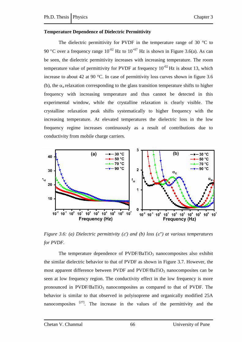
Ph.D. Thesis Physics Chapter 3
Chetan V. Chanmal 66 University of Pune
Temperature Dependence of Dielectric Permittivity
The dielectric permittivity for PVDF in the temperature range of 30 °C to
90 C over a frequency range 10-02
Hz to 10+07
Hz is shown in Figure 3.6(a). As can
be seen, the dielectric permittivity increases with increasing temperature. The room
temperature value of permittivity for PVDF at frequency 10-02
Hz is about 13, which
increase to about 42 at 90 °C. In case of permittivity loss curves shown in figure 3.6
(b), the a relaxation corresponding to the glass transition temperature shifts to higher
frequency with increasing temperature and thus cannot be detected in this
experimental window, while the crystalline relaxation is clearly visible. The
crystalline relaxation peak shifts systematically to higher frequency with the
increasing temperature. At elevated temperatures the dielectric loss in the low
frequency regime increases continuously as a result of contributions due to
conductivity from mobile charge carriers.
Figure 3.6: (a) Dielectric permittivity (') and (b) loss (") at various temperatures
for PVDF.
The temperature dependence of PVDF/BaTiO3 nanocomposites also exhibit
the similar dielectric behavior to that of PVDF as shown in Figure 3.7. However, the
most apparent difference between PVDF and PVDF/BaTiO3 nanocomposites can be
seen at low frequency region. The conductivity effect in the low frequency is more
pronounced in PVDF/BaTiO3 nanocomposites as compared to that of PVDF. The
behavior is similar to that observed in polyisoprene and organically modified 25A
nanocomposites [27]
. The increase in the values of the permittivity and the

Ph.D. Thesis Physics Chapter 3
Chetan V. Chanmal 67 University of Pune
displacement of the peak maximum of permittivity with the temperature are
characteristic behavior of dielectric dispersion. Most generally, in the system with low
conductivity the rapid increase of the permittivity at very low frequency is due to the
electrode polarization and the effect of electrode polarization can completely mask the
low frequency relaxation.
Figure 3.7: (a) Dielectric permittivity (') and (b) loss (") at various temperatures
for PVDF/BaTiO3- 30%.
3.I.3.4 Electric Modulus Formalism
When electrode polarization effect dominates the dielectric loss spectra and
masks relaxation spectra in the low frequency region, electric modulus formalism is
used to resolve low frequency relaxations. The electric modulus formalism is
introduced by McCrum et al [14]
and it is used to study electrical relaxation
phenomena in many polymers [28-30]
. As the dielectric modulus is derived from the
dielectric permittivity and loss values, it contains the similar information of the
sample, however contributions from electrode polarization are reduced.
The electric modulus can be defined by the following equation:
Where and are the real and the imaginary part of electric modulus
respectively, and ε' and ε″ are the real and the imaginary part of dielectric permittivity.

Ph.D. Thesis Physics Chapter 3
Chetan V. Chanmal 68 University of Pune
Figure 3.8: Dielectric loss modulus (M") as a function of frequency and temperature for
(a) PVDF (b) PVDF/BaTiO3 –10% (c) PVDF/BaTiO3 –20% (d) PVDF/BaTiO3 –30%
Figure 3.8 (a) shows typical 3-d plots of dielectric modulus spectra for pure
PVDF at various temperatures as a function of frequency. Two relaxation processes
can be clearly observed in the M″ curves. The relaxation peak at high frequency side
is identified as fast symmetric crystalline relaxation and it shifts to higher frequency
with the increasing temperature. At high temperature, another relaxation peak appears
in modulus spectra. This relaxation is attributed to Maxwell-Wagner-Sillars (MWS)
polarization which can be seen in the heterogeneous materials and is also known as
interfacial polarization. At temperature above 70 °C the MWS relaxation peak starts
10-3100
103106
109Frequency [Hz]
020
40
60
Mo
du
lus'' 1
0-3
0
50
100
150
200
Tem
pera
ture
[°C
]
PVDF + BaTiO3 -20%-Ag Paste AC Volt [Vrms]=1.00
10-3100
103106
109Frequency [Hz]
020
40
60
Mo
du
lus'' 1
0-3
0
50
100
150
200
Tem
pera
ture
[°C
]
PVDF -BaTiO3- 10%-temp sweep AC Volt [Vrms]=1.00
10-3100
103106
109Frequency [Hz]
020
40
60
Mo
du
lus''
10
-3
0
50
100
150
200
Tem
pera
ture
[°C
]
PVDF -Ag Paste AC Volt [Vrms]=1.00
10-3100
103106
109Frequency [Hz]
010
20
30
40
Mo
du
lus'' 1
0-3
0
50
100
150
200
Tem
pera
ture
[°C
]
PVDF + BaTiO3 -30% AC Volt [Vrms]=1.00
c
MWS MWS
MWS MWS
c
c c
(a)
(c) (d)
(b)

Ph.D. Thesis Physics Chapter 3
Chetan V. Chanmal 69 University of Pune
appearing in PVDF whereas in PVDF/BaTiO3 nanocomposites the MWS peak is seen
at higher temperature about 90 °C. In semicrystalline polymers, the crystalline regions
are dispersed in amorphous matrix and MWS relaxation is observed in these materials
due to the differences in the conductivity and permittivity values of the crystalline and
amorphous phases [31, 27]
. For heterogeneous composite, an interfacial polarization is
almost always present because of filler additives or even impurities that migrate
towards the interface [32]
. The modulus relaxation peaks (M'') for both relaxation
processes shift to a higher frequency with increasing temperature. In addition, there is
no significant change in the dielectric relaxation peak height for crystalline relaxation
process. However, the intensity of dielectric relaxation peak at low frequency side
increases with temperature and peak broadening decreases signifying asymmetric
nature of MWS relaxation. Similar dielectric relaxation in the low frequency region
below that of crystalline relaxation (c) is noted in earlier work on PVDF and this
relaxation is ascribed to be interfacial or MWS polarization [33]
.
The relaxation peaks of PVDF and PVDF/BaTiO3 nanocomposites as a
function of frequencies at 120 °C are shown in Figure 3.9. In case of c relaxation,
peak appears at same frequency for polymer and nanocomposites, whereas MWS
peak for PVDF/BaTiO3 nanocomposites shifts to lower frequency as compared to
PVDF. The graph also clearly shows that the intensity of MWS relaxation decreases
with increasing content of BaTiO3, which is characteristic of MWS relaxation [34, 35]
.
Similar behavior is observed for PVDF/BaTiO3 nanocomposites at all measured
temperatures. It is also noteworthy that the dielectric loss of the nanocomposites
arises primarily from the polymer matrices and is almost independent of the volume
content of the BaTiO3 filler.

Ph.D. Thesis Physics Chapter 3
Chetan V. Chanmal 70 University of Pune
Figure 3.9: Comparison of dielectric modulus spectra of PVDF and PVDF/BaTiO3
nanocomposites at 120 °C as a function of frequency.
3.I.3.5 Activation Energy
The temperature dependence for crystalline and MWS relaxations is further
analyzed by plotting the logarithm of relaxation time log ( ) at the peak maxima
versus reciprocal of temperature (1000/T) as shown in Figure 3.10. The relaxation
time, defined as the inverse of frequency maximum, decreases with increasing
temperature due to enhancement in the mobility of charge carriers at high
temperature. The temperature dependence of dielectric relaxation can be well
described by the Arrhenius type behavior.
The plot for crystalline relaxation process exhibits a linear dependence of
logarithmic relaxation time log ( ) versus inverse of temperature over a wide
temperature range for all composite films and follows Arrhenius equation:
Where, = relaxation time corresponding to frequency maximum
Ea = Activation energy
K = Boltzmann’s constant

Ph.D. Thesis Physics Chapter 3
Chetan V. Chanmal 71 University of Pune
From the Arrhenius equation, the activation energy (Ea) can be determined
from the slope of the curve.
Figure 3.10: Activation energy plot for (a) crystalline relaxation and (b) MWS
relaxation showing Arrhenius type behavior.
The slope of the best fitted straight lines gives the activation energy. The
activation energy for the crystalline relaxation peak was found to be about 0.41 eV for
PVDF as well as for PVDF/BaTiO3 nanocomposites. This value is in good agreement
with the reported value of (0.40 eV) activation energy for crystalline relaxation (c) in
PVDF [36]
.
The MWS relaxation also shows Arrhenius type behavior indicating relaxation
is thermally activated process. The activation energy for MWS relaxation slightly
decreases in case of PVDF/BaTiO3 nanocomposites. Table 3.1 summarizes the
calculated parameters for crystalline (c relaxation) and MWS relaxations.
Table 3.1: Fitting parameters for crystalline relaxation and MWS relaxation.
Composition
Crystalline relaxation (c) MWS relaxation
Log (sec) Ea (eV) Log (sec) Ea (eV)
PVDF -16.4 0.42 -23.5 1.8
PVDF/BaTiO3-10% -16.3 0.41 -22.6 1.7
PVDF/BaTiO3-20% -16.2 0.41 -21.1 1.6
PVDF/BaTiO3-30% -15.9 0.40 -20.7 1.60
(a) (b)
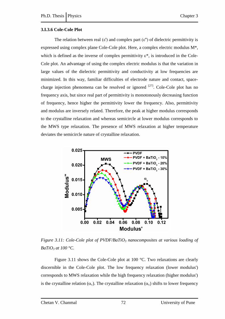
Ph.D. Thesis Physics Chapter 3
Chetan V. Chanmal 72 University of Pune
3.I.3.6 Cole-Cole Plot
The relation between real (ε') and complex part (ε'') of dielectric permittivity is
expressed using complex plane Cole-Cole plot. Here, a complex electric modulus M*,
which is defined as the inverse of complex permittivity *, is introduced in the Cole-
Cole plot. An advantage of using the complex electric modulus is that the variation in
large values of the dielectric permittivity and conductivity at low frequencies are
minimized. In this way, familiar difficulties of electrode nature and contact, space-
charge injection phenomena can be resolved or ignored [27]
. Cole-Cole plot has no
frequency axis, but since real part of permittivity is monotonously decreasing function
of frequency, hence higher the permittivity lower the frequency. Also, permittivity
and modulus are inversely related. Therefore, the peak at higher modulus corresponds
to the crystalline relaxation and whereas semicircle at lower modulus corresponds to
the MWS type relaxation. The presence of MWS relaxation at higher temperature
deviates the semicircle nature of crystalline relaxation.
Figure 3.11: Cole-Cole plot of PVDF/BaTiO3 nanocomposites at various loading of
BaTiO3 at 100 °C.
Figure 3.11 shows the Cole-Cole plot at 100 °C. Two relaxations are clearly
discernible in the Cole-Cole plot. The low frequency relaxation (lower modulus')
corresponds to MWS relaxation while the high frequency relaxation (higher modulus')
is the crystalline relation (c). The crystalline relaxation (c) shifts to lower frequency

Ph.D. Thesis Physics Chapter 3
Chetan V. Chanmal 73 University of Pune
without any composition dependence as a result of incorporation of BaTiO3. Similar
shift to lower frequencies is observed for MWS relaxation but with some composition
dependence. The shift of relaxation process to lower frequency with increase in filler
content indicates the characteristic of MWS nature [37]
. The shift in the Cole-Cole
plots towards the origin with increasing BaTiO3 content implies an increase in the
relaxation time with heterogeneity.
3.I.4 Conclusions
PVDF/BaTiO3 nanocomposites are prepared using simple melt mixing
technique. The BaTiO3 nanoparticles are well dispersed in the PVDF matrix as
evidenced by the scanning electron micrographs. The dielectric permittivity increases
with increasing BaTiO3 content. The room temperature dielectric spectra shows two
relaxations processes corresponding to the glass transition (a) and crystalline (c)
relaxation while at high temperature another low frequency relaxation is observed
which is attributed to the MWS relaxation. The temperature dependence of
c-relaxation and MWS relaxation follows Arrhenius type behavior.
Ph.D. Thesis Physics Chapter 3
Chetan V. Chanmal 74 University of Pune
Section II: Electrospun PVDF/BaTiO3 Nanofibers for Low Thermal Emissivity
3.II.1 Introduction
In this section we present the fabrication of PVDF/BaTiO3 nanofibers by
electrospinning process. The effect of addition of BaTiO3 on the thermal emissivity of
electrospun fiber was studied. A prototype instrument based on the principles of black
body radiation was built in the laboratory and used for the measurement of the
thermal emissivity. A calibration curve is plotted using reference standard materials
and this curve was to calculate the thermal emissivity of polymer nanocomposites.
3.II.2 Experimental
The solution (15 wt%/vol) of PVDF was prepared by dissolving PVDF pellets
in mixture of DMF and acetone (1:1 ratio) and was heated at 60 °C for 30 min to
make the solution homogenous. Solution for PVDF/BaTiO3 nanocomposites were
prepared by adding known quantity of BaTiO3 nanoparticles (5 wt%) to the PVDF
solution followed by ultrasonication. The viscous solution of PVDF/BaTiO3
nanocomposites was transferred to glass syringe for electrospinning. The glass
syringe with 5 ml capacity and a stainless steel needle with 0.8 mm diameter was used
for electrospinning. A positive voltage of 15 KV was applied between needle and the
collector plate. The fibers were collected onto grounded aluminium foil. The polymer
solution was electrospun at a flow rate of 0.075 ml/min on to collector kept at 15 cm
from the needle. All electrospinning experiments were carried out at room
temperature. The nanofibers mats were dried in vacuum oven at 60 °C prior to
characterization. The electrospun mats were characterized for morphology and
structural analysis.
Emissivity Measurement using Thermopile as a Sensor
Most generally, Thermopile is used to determine temperature by assuming an
emissivity for the object. In the present work we will use thermopile to determine the
emissivity of a variety of materials when the surface temperatures kept at constant
temperature using PID controller.
A thermopile is basically a number of thermocouples connected in series.
When two dissimilar metals connected kept at different temperature then a voltage
appears across the junctions, this principle is called “Seebeck effect” and same is used

Ph.D. Thesis Physics Chapter 3
Chetan V. Chanmal 75 University of Pune
in thermocouple. It is used to convert thermal potential difference into electric
potential difference. When temperature difference appears across the junction,
because of the difference in the work function of two metals, an electric voltage is
generated across the junction. The generated electric voltage is very small in mV and
it is proportional to power radiated. The thermopile measures temperature by focusing
infrared radiation emitted by an object onto a thermopile detector. The thermopile is
heated by this radiation and its equilibrium temperature is proportional to the emissive
power of the object which, from the Stefan-Boltzmann law, is
P = (T) T4
Where, P is Power radiated from the material, (T) is the Emissivity of the
object, Stefan Boltzmann’s constant and T is the temperature
If the temperature is held constant, then power radiated from sample is
proportional to the emissivity of the material.
P (when temperature is kept constant)
This method involves measurement of the electric voltage generated at a
constant temperature. The measurement set up consists of detector housing assembly
in which IR sensor and sample are enclosed in single housing that avoids external
radiation effects. To isolate the detector form sources of radiation other than object, a
Teflon sheet is attached in front of detector to ensure thermal isolation of the detector.
The measurement sample is firmly place on an Aluminium block with good thermal
contact and the metal block is heated by using resistive heating technique.
Figure 3.12: Thermopile Set-up Block Diagram for emissivity measurement.

Ph.D. Thesis Physics Chapter 3
Chetan V. Chanmal 76 University of Pune
The block diagram of emissivity measurement instrument is shown in figure
3.12. During the measurement, the temperature of the sample is accurately maintained
at 60 °C using PID controller 2216L from Eurotherm. The temperature stabilization is
better than 0.1 °C. The temperature was chosen so that the maximum emission,
calculated from Weins displacement law, appears at wavelength of 7.8 m. The
detector is mounted in front of the sample at a distance of 15 mm. The distance
between sample and detector is optimized by taking field of view concept into
account which gives the maximum sensitivity. Field of view is the solid angle through
which detector see the object. Electromagnetic radiation (Infrared ray) emitted from
sample is focused onto thermopile. Based on principles of thermoelectric effects,
thermopile sensor converts the incident thermal radiation into the electric signal in the
form of electric voltage. As discussed in the theory of emissivity measurement, this
electric signal generated is proportional to emissivity of the material provided
temperature is held constant. External electronic circuit is used to activate the
thermopile sensor. As the voltage received is in millivolts, a low noise amplifier with
the gain of 1000 is used for the amplification. A DAQ card from Labview is installed
in computer to receive the data in digital form. The data received is stored on
computer using Labview software. The data received can be retrieved in the Excel
format. Figure 3.13 shows the photographs of emissivity measurement unit in the lab.
Figure 3.13: Photographs of prototype instrument for the measurement of thermal
emissivity.
PID
controller Sample
holder

Ph.D. Thesis Physics Chapter 3
Chetan V. Chanmal 77 University of Pune
Emissivity Measurement Procedure
The samples were heated to set temperature with accurate heating control
using PID temperature controller. Black body is first loaded into the sample holder.
Radiation emitted from black body is directed towards detector, which in turn
produces a voltage signal response. Thermal voltage from black body is recorded and
saved. Next measurement sample is loaded in sample holder, and its thermal voltage
is recorded. Using following relation emissivity of sample is calculated:
ε polymer =
× ε black body
Where, ε polymer is emissivity of polymer, ε black body is emissivity of black body, Vs is
thermal voltage from polymer sample and Vbb is thermal voltage from black body.
Calibration of the instrument
The instrument is initially calibrated by using standard set of samples with
known values of thermal emissivity (shown in table 3.2). Figure 3.14 shows
calibration graph of thermopile for thermal voltage against the reported emissivity of
standard materials.
Table 3.2: Reported emissivity values for standard samples used and the measured
thermal voltage.
Calibration graph of thermopile shows that response of the thermopile is linear with r2
value of 0.99. The nature of graph indicates that emissivity is directly proportional to
thermal voltage from thermopile. With this calibration graph emissivity of unknown
material can be predicted when thermal voltage is measured from thermopile. The
Sr.
No.
Standard Material Reported
Emissivity
Thermal Voltage
(mV)
1. Glass 0.92 3.3
2. Anodized Aluminium 0.8 2.95
3. Cotton Cloth 0.75 2.78
4. Silver paste 0.49 2.06
5. Lead (ruf) 0.43 1.84
6. Lead (Polish) 0.28 1.44
7. Stainless steel 0.16 1.4
8. Al-Foil 0.09 1.16
9. Copper 0.1 1.18

Ph.D. Thesis Physics Chapter 3
Chetan V. Chanmal 78 University of Pune
emissivity values obtained were also confirmed with measurement by using IR
camera and the results were found to match closely.
Figure 3.14: Calibration Graph at 60 °C of Thermopile sensor for emissivity
measurement
3.II.3 Results and Discussion
3.II.3.1 Morphology
Figure 3.15 depicts the scanning electron micrographs (SEM) of PVDF and
PVDF/BaTiO3 electrospun mats. SEM images show the fiber morphology of
PVDF/BaTiO3 electrospun mats. It can be seen that the fibers are randomly oriented.
Under the processing conditions used in the present study, round fibers with diameters
in the range of 100–200 nm are observed.
Figure 3.15: SEM micrograph of PVDF and PVDF/BaTiO3 electrospun nanofibers
(inset shows the histogram of fiber size distribution).

Ph.D. Thesis Physics Chapter 3
Chetan V. Chanmal 79 University of Pune
3.II.3.2 Structural Analysis
Figure 3.16 illustrates the X-ray diffraction patterns for electrospun PVDF and
PVDF/BaTiO3 nanocomposites. As can be seen from the diffraction patterns, PVDF
electrospun fibers show two peaks at 2 values of about 19.9° and 18.5°
corresponding to the α phase of PVDF. A very fine shoulder appears in PVDF
electrospun fiber at 20.8° which corresponds to β phase of PVDF [38]
. This indicates
that PVDF crystallizes mainly in α phase during electrospinning process. However,
X-ray diffraction study of PVDF/BaTiO3 electrospun fiber shows a single diffraction
peak at about 20.8° which corresponds distinctively to β phase of PVDF. Thus, X-ray
diffraction study shows that addition of BaTiO3 and electrospinning process assist in
the formation β phase of PVDF. This phase formation can be explained on the basis
of electrospinning process. Application of high voltage in electrospinning process
which acts as a poling field to dipoles in PVDF and stretching of electrospun fiber
assists in the enhancement of β phase in PVDF. Thus, these two processing
parameters viz. stretching and application of high electric field in electrospinning
provides an advantage over other techniques such as melt mixing or solution casting
where after the preparation of nanocomposites either stretching or poling has to be
done separately to generate β phase in PVDF. Additional peaks at 32°, 39° and 45°
confirms the presence of (110), (111) and (200) planes of BaTiO3 nanoparticles
respectively.
Figure 3.16: X-ray diffraction patterns for electrospun PVDF and PVDF/BaTiO3
nanocomposites.

Ph.D. Thesis Physics Chapter 3
Chetan V. Chanmal 80 University of Pune
Figure 3.17 shows the ATR-FTIR spectra of electrospun fiber mats of PVDF
and PVDF/BaTiO3 nanocomposite. The electrospun mats of PVDF nanocomposites
show peaks at 613,762,840, 874, 975, 1072, 1179, 1275, and 1400 cm-1
. The peaks at
613, 762, and 975 cm-1
are attributed to phase of PVDF while the bands at 840 and
1275 cm-1
are attributed to the β phase of PVDF [16]
. The peaks at 613 and 762 cm-1
can be assigned to the CF2 bending and skeletal bending of C (F)-C (H)-C (F) of
phase of PVDF while the peak at 975 cm-1
can be assigned to CH2 bending mode of
phase of PVDF. The peak at 840 cm-1
is due to the CH2, CF2 rocking and asymmetric
stretching in β phase of PVDF. This clearly shows that the electrospun mats of PVDF
exhibit a mixed structure of and β phase. A comparison of FTIR spectra of PVDF
and PVDF/BaTiO3 electrospun mats demonstrates that the absorption bands (613,
762, and 975 cm-1
), characteristic of phase absorption peaks are diminished in
intensity as a result of BaTiO3 loading. This observation indicates that the
crystallization of PVDF in PVDF/BaTiO3 during electrospinning promotes formation
of β phase of PVDF under the set of experimental conditions used. It can be envisaged
that crystallization of polymer in electrospinning process is associated with high shear
stress and extremely rapid structure formation [39]
. Accordingly, stretching of the
electrospinning jet could result in change in molecular conformation which facilitates
formation of β phase in PVDF.
Figure 3.17: ATR-FTIR of electrospun PVDF and PVDF/BaTiO3 nanocomposite.
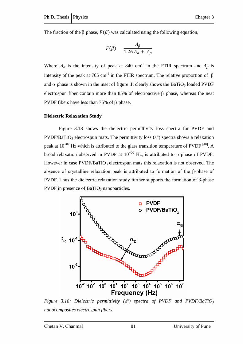
Ph.D. Thesis Physics Chapter 3
Chetan V. Chanmal 81 University of Pune
The fraction of the phase, was calculated using the following equation,
Where, is the intensity of peak at 840 cm-1
in the FTIR spectrum and is
intensity of the peak at 765 cm-1
in the FTIR spectrum. The relative proportion of
and phase is shown in the inset of figure .It clearly shows the BaTiO3 loaded PVDF
electrospun fiber contain more than 85% of electroactive phase, whereas the neat
PVDF fibers have less than 75% of phase.
Dielectric Relaxation Study
Figure 3.18 shows the dielectric permittivity loss spectra for PVDF and
PVDF/BaTiO3 electrospun mats. The permittivity loss (") spectra shows a relaxation
peak at 10+07
Hz which is attributed to the glass transition temperature of PVDF [40]
. A
broad relaxation observed in PVDF at 10+00
Hz, is attributed to α phase of PVDF.
However in case PVDF/BaTiO3 electrospun mats this relaxation is not observed. The
absence of crystalline relaxation peak is attributed to formation of the β-phase of
PVDF. Thus the dielectric relaxation study further supports the formation of β-phase
PVDF in presence of BaTiO3 nanoparticles.
Figure 3.18: Dielectric permittivity ('') spectra of PVDF and PVDF/BaTiO3
nanocomposites electrospun fibers.

Ph.D. Thesis Physics Chapter 3
Chetan V. Chanmal 82 University of Pune
3.II.3.3 Thermal Emissivity of PVDF/BaTiO3 Nanofibers
The electrospun nanofibers were tested for low thermal emissivity application.
For a comparative study, emissivity of melt pressed bulk samples of PVDF and
PVDF/BaTiO3 nanocomposite were also measured. Table 3.3 presents the values of
emissivity for electrospun mats as well as melt pressed films of PVDF and
PVDF/BaTiO3 nanocomposite. The result indicates that, as compared to melt pressed
films the emissivity of electrospun mat is lower in PVDF and PVDF/BaTiO3
nanocomposite fibers. Secondly, the incorporation of BaTiO3 in PVDF results in
significantly lower values of emissivity than PVDF electrospun fibers. When the
emissivity values of the electrospun fiber mats are compared it is observed that the
value decreased from 0.7 for PVDF to 0.64 for the PVDF/BaTiO3 mat. The decrease
in the value of emissivity in PVDF/BaTiO3 nanocomposite suggests presence of
interfacial interactions between PVDF and BaTiO3 nanoparticles [41]
. Further, the
reduction in emissivity can also be attributed to the non-woven porous morphology of
electrospun membrane which reduces the emissivity due to internal scattering [42]
. The
porosity of the material cancels any emission contribution from the underlying
materials due to scattering in the homogenous system.
Table 3.3: Infrared emissivity of Electrospun PVDF and PVDF/BaTiO3
nanocomposite.
Sr.
No.
Sample Infrared
Emissivity
1. PVDF melt pressed film 0.86
2. PVDF/BaTiO3 (5 % by wt %) melt pressed film 0.82
3. PVDF Electrospun mat 0.7
4. PVDF/BaTiO3 (5% by wt %) Electrospun mat 0.64

Ph.D. Thesis Physics Chapter 3
Chetan V. Chanmal 83 University of Pune
3.II.4 Conclusions
Fibers of PVDF/BaTiO3 nanocomposite were prepared by electrospinning
technique. The diameter of electrospun fibers was between 100-200 nm. Structural
characterization of electrospun mats show that PVDF crystallized in mixed α and β
phase whereas addition of BaTiO3 nanoparticles to PVDF matrix was found to
enhance β phase structure in PVDF as evidenced by X-ray diffraction and ATR-FTIR
analysis. The dielectric relaxation spectra also supported the presence of β phase in
PVDF/BaTiO3 electrospun mats. Thermal emissivity of PVDF/BaTiO3 electrospun
mats was found to be lower than melt pressed PVDF/BaTiO3 sample. In general,
addition of BaTiO3 has shown to enhance structural properties of PVDF.
3.II.5 References
1. Jin-Kai Yuan, Zhi-Min Dang, Sheng-Hong Yao, Jun-Wei Zha, Tao Zhou,
Sheng-Tao Li, Jinbo Bai, J. Mater. Chem., 2010, 20, 2441–2447.
2. C.K. Chiang, R. Popielarz, Ferroelectrics, 2002, 275, 1-9.
3. G. A. Kontos, A. L. Soulintzis, P. K. Karahaliou, G. C. Psarras, S. N. Georga,
C.A. Krontiras, M. N. Pisanias, Express polymer letters, 2007, 1, 781-789.
4. G. C. Psarras, K. G. Gatos, P. K. Karahaliou, S. N. Georga, C. A. Krontiras, J.
Karger-Kocsis, Express polymer letters, 2007, 1, 837-845.
5. H. Ishida, S. Campbell, John Blackwell, Chem. Mater., 2000, 12, 1260-1267.
6. Jr. R. Gregorio, M. Cestari, Journal of Polymer Science: Part B: Polymer
Physics, 1994, 32, 859-870.
7. K.P. Pramoda, A. Mohamed, In Yee Phang, L. Tianxi, Polymer Int. 2005, 54,
226-232.
8. Jr. R. Gregorio, E.M. Ueno, Journal of Material Science, 1999, 34, 4489-4500.
9. Rinaldo Gregorio, Jr., Journal of Applied Polymer Science, 2006, 100, 3272–
3279.
10. Z.M. Dang, H.Y. Wang, Y.H. Zhang, J.Q. Qi, Molecular Rapid
Communications, 2005, 26, 1185-1189.
11. R. Sekar., A.K. Tripathi, P. K. Pillai, Materials Science and Engineering, B5,
1989, 33-36.
12. F. Kremer, Journal of Non-crystalline solids, 2000, 305, 1-9.

Ph.D. Thesis Physics Chapter 3
Chetan V. Chanmal 84 University of Pune
13. H. Djidjelli, D. Benachour, A. Boukerrou, O. Zefouni, J. Martinez-Vega, J.
Farenc, M. Kaci, Express polymer letters, 2007, 1, 846-852.
14. N.G. McCrum, B.E. Read, G. Williams, “Anelastic and viscoelastic behavior of
polymeric solids”, London, Wiley, (1967).
15. S. F. Mendes, C. M. Costa, C. Caparros, V. Sencadas, S. Lanceros-Mendez, J
Mater Sci., 2011, 011, 5916.
16. S.A. Madbouly, J.A. Otaigbe, Polymer, 2007, 48, 4097-4107.
17. J. Mijovic, Jo-wing Sy, T.K. Kwei, Macromolecules, 1997, 30, 3042-3050.
18. L. Hongbo, Z. Xingyuan, Journal of Macromolecular science, Part B: Physics,
2006, 45, 933-944.
19. A. Linares, A. Nogales, D. R. Rueda, T.A. Ezquerra, Journal of Polymer
Science: Part B: Polymer Physics, 2007, 45, 1653-1661.
20. Jo Wing Sy, Jovan Mijovic, Macromolecules, 2000, 33, 933-946.
21. A. Bello, E. Laredo, M. Grimau, Physical Review B, 1999, 60, 12764- 12774.
22. V.K. Valetine, A.M. Inna, V.M. Grigory, N.V. Gavrilov, N.P. Bessonova,
Journal of Applied Polymer Science, 2007, 105, 1107-1117.
23. Y. Takahashi, K. Miyaji, Macromolecules, 1983, 16, 1789- 1792.
24. K. Nakagawa, Y. Ishida, Journal of Polymer Science, 1973, 11, 1503-1533.
25. M. Yoshihisa, M. Hideki, A. Kenjiro, Journal of Polymer Science: Polymer
Physics, 1980, 18, 597- 606.
26. Y. Miyamoto, H. Miyaji, K. Asai, Journal of Polym. Sci. Part B: Polym. Phys.,
1980, 18, 597606.
27. J. Mijovic, L. Hyuangki, J. Kenny, J. Mays, Macromolecules, 2006, 39, 2172-
2182.
28. G.M. Tsangaris, G.C. Psarras, N. Kouloumbi, Journal of materials science,
1998, 33, 2027-2037.
29. H.W. Starkweather, P. Avikian, Journal of Polymer Science Polymer Physics,
1992, 30, 637- 641.
30. I.M. Hodge, A. Eisenberg, Journal of non-crystalline solids, 1978, 27, 441- 443.
31. M. Arous, B. I. Amor, A. Kallel, Z. Fakhfakh, G. Perrier, Journal of Physics and
Chemistry of Solids, 2007, 68, 1405-1414.
32. G.C. Psarras, E. Manolakaki, G.M. Tsangaris, Composites: Part A, 2003, 34,
1187-1198.

Ph.D. Thesis Physics Chapter 3
Chetan V. Chanmal 85 University of Pune
33. H. Sasabe, S. A. Saito, H. Kakutani, Journal of polymer science: Part A-2,
1969, 7, 1405-1414.
34. Y. Suzhu, P. Hing, H. Xiao, Journal of Applied Physics, 2000, 88, 398-405.
35. J.H. Daly, M. J. Guest, Journal of Materials Science Letters, 1992, 11, 1271-
1273.
36. E. Tuncer, M. Wagener, R. Gerhard-Multhaupt, Journal of Non-crystalline
solids, 2005, 351, 2917-2921.
37. H. Hammamia, M. Arous, M. Lagache, A. Kallel, Journal of Alloys and
Compounds, 2007, 430, 1–8.
38. Ganji Zhong, Lifeng Zhang, Run Su, Ke Wang, Hao Fong, Lei Zhu, Polymer,
2011, 52, 2228-2237.
39. Z.M. Huang, Y.Z. Zhang, M. Kotaki, S. Ramakrishna, Composites science and
technology, 2003, 63, 2223-2253.
40. C.V. Chanmal, J.P. Jog, Express Polymer Lett., 2008, 2, 294-301.
41. Z.M. Dang, H.P. Xu , H.Y. Wang, Appl. Phys. Lett., 2007, 90, 012901.
42. H. Wu, J. Fan, N.J. Du, Appl. Polym. Sci., 2007, 106,576-583.

Chetan V. Chanmal 86 University of Pune
Chapter 4
Strong Electric Field Modulation of Transport
in PVDF/MWCNT Nanocomposite near the
Percolation Threshold
This chapter describes the fabrication of PVDF/MWCNT nanocomposite thin films
by pulsed laser deposition and the study of their structural and dielectric properties.
The addition of MWCNT results in crystallization of PVDF into ferroelectric phase
and an enhancement in the dielectric permittivity at relatively low dielectric loss. The
aspect ratio of MWCNT was found to decrease in the PLD process which effectively
increases the percolation threshold in nanocomposites and allows the higher loading
of MWCNTs into polymer matrix. The nanocomposites also exhibit an increase in the
conductivity due to addition of MWCNT. The nanocomposites material when used as
a channel layer in the field effect device architecture showed high modulation in the
drain current.
Part of the work presented in this chapter has been published in following
journals:
1.Chetan Chanmal, Meenal Deo, Abhimanyu Rana, Jyoti Jog, Satishchandra
Ogale, Solid State Communications, 2011, 151, 1612–1615.
2.Chetan Chanmal, Meenal Deo, Jyoti Jog, Applied Surface Science, 2011,
258, 1256–1260.
Ph.D. Thesis Physics Chapter 4
Chetan V. Chanmal 87 University of Pune
4.1 Introduction
Polymer based composites with high dielectric constant and low dielectric
losses are of great interest in embedded capacitor technology as they provide
advantage in size and cost reduction. In this context, ferroelectric polymers have
received increasing interest in recent years due to their potential applications in
embedded capacitors, gate dielectrics and charge storage applications [1-3]
. Generally,
polymers have low dielectric permittivity and the dielectric properties of polymers
can be enhanced by addition of ferroelectric nanofillers [4, 5]
. However, this technique
requires higher filler loading which is detrimental to the mechanical properties of the
polymer. Another method of increasing dielectric permittivity which has gained
significant interest is to add metallic nanofiller in the vicinity of percolation threshold
[6, 7]. The dielectric permittivity in this case is found to increase by several orders of
magnitude when filler loading is near to percolation threshold. One of the most
studied nanofiller in this context is multiwalled carbon nanotubes (MWCNT). In case
of MWCNTs, percolation threshold depends on many parameters like processing
method, polymer matrix and nature of carbon nanotubes [8, 9]
.
Although, percolative nanocomposites exhibit a significant increase in the
dielectric permittivity, there are few challenges in making these systems useful for
commercial applications. First, near the percolation threshold due to increase in the
conductivity, a remarkable increase in the losses are generally observed [8]
. Secondly,
to realize the true potential of these nanocomposites in the field of micro-electronics
one needs to prepare the materials in thin film phase. Many researchers have studied
the polymer based MWCNT nanocomposites in bulk and thick films [10-13]
.
Along these lines, in the present work we have successfully fabricated the thin
films Poly (vinylidene fluoride) (PVDF)/MWCNT nanocomposite by pulsed laser
deposition (PLD). PLD has an advantage over other techniques of depositing polymer
composite films as it is a dry process which is also compatible with other vacuum
processing methods [14, 15]
. PVDF is used as a polymer matrix which is important for
its ferroelectric properties. PVDF is a semi-crystalline polymer and depending on the
type of conformation it exhibits five polymorphic phases, namely, TTTT for phase,
TGTG’ for and phases, TTTGTTTG’ for and phases [16]
. Out of these, phase
attracts maximum research and industrial interest due to its ferroelectric properties [17]
.
The orthorhombic phase is normally obtained with different techniques such as

Ph.D. Thesis Physics Chapter 4
Chetan V. Chanmal 88 University of Pune
mechanical stretching of PVDF, addition of clay, and poling in a strong electric field
[18-21]. The specific synergistic interaction between MWCNT and PVDF is known to
nucleate the phase in solution prepared PVDF/MWCNT nanocomposites [22, 23]
.
Indeed, we find that incorporation of MWCNT stabilizes the important piezoelectric
-phase PVDF in our thin films even though we start with a bulk target comprising of
the non-polar -phase of PVDF. Moreover, the short interaction times and non-
equilibrium conditions imposed by the PLD process are found to be useful in
achieving good dispersion of the filler in the polymer matrix. Thus, detailed
characterization of the nanocomposites carried out shows that MWCNTs not only
help in enhancing the ferroelectric -phase in the pulsed laser deposited polymeric
film, but also provide adequate dispersion of MWCNTs leading to high values of
dielectric permittivity over a broad range of frequencies.
As the fabricated nanocomposite shows a remarkable enhancement in the
conductivity, these nanocomposite films were further studied for channel layer in field
effect device architecture. Field effect transistor (FET) is perhaps the most significant
device in any modern electronic chip architecture. Not surprisingly, there have been a
large number of studies on FETs based on semiconducting and inorganic materials as
transport channels over the past several decades [24-26]
. With the growing emphasis on
flexible electronics for novel futuristic technologies as well as to explore novel
materials alternatives for non-flexible electronics, materials such as conducting and
semiconducting carbon forms (CNTs, graphene) are now being actively explored
[27,28]. In most such studies a thin uniform layer of a single semiconducting polymer or
carbon form is used, and organic FETs (O-FET) with functionalities comparable to
the established inorganic semiconductor based devices have been demonstrated [29, 30]
.
However, polymer based nanocomposites as a channel layer was examined only
scarcely in field effect devices [31, 32]
. In this work we use thin film of a functional
nanocomposite comprising of a ferroelectric polymer (PVDF) and MWCNTs as an
active channel layer and demonstrate that a strong electric field modulation of carrier
transport can be realized therein, just below the percolation threshold.

Ph.D. Thesis Physics Chapter 4
Chetan V. Chanmal 89 University of Pune
4.2 Experimental
4.2.1 Materials
PVDF (Grade Solef 1008) obtained from Solvay, Belgium was used in this
study. Multiwalled carbon nanotubes MWCNTs with (OD = 10-20 nm, ID = 5-10 nm
& length = 0.5 to 200 m) were procured from Aldrich chemicals and used without
any further chemical modification. The density of MWCNT was 2.1 g cm-3
. The
details of the properties of these materials are presented in chapter 2.
4.2.2 PLD Processing of PVDF/MWCNT Thin Films
Initially, nanocomposites of PVDF/MWCNT were prepared by melt mixing
method in Haake Polylab batch mixer. The MWCNTs were mixed with PVDF pellets
and fed to the batch mixer. The batch mixer was operated at a temperature of 200 °C,
screw speed of 60 RPM and residence time of 5 minutes. Subsequently the pellets of
the nanocomposites were prepared by hot press technique. The disk shaped pellets of
PVDF/MWCNT nanocomposites were used as the targets for Pulsed Laser Deposition
(PLD). In the PLD process, KrF excimer laser ( = 248 nm, pulse width 20 ns) at an
energy density of 1.5 J/cm2
was used for ablation of polymer. The copper foil was
used as a substrate in the PLD deposition. The nanocomposites were characterized for
structural, morphology, dielectric and various other properties. Following table shows
the sample coding and composition of PVDF/MWCNT nanocomposites. Volume
percentage was calculated using the value of density of MWCNT as 2.1 g cm-3
.
Table 4.1: Sample codes and compositions of PLD deposited PVDF/MWCNT
nanocomposites.
Sample
Code
Wt% loading of MWCNT Volume% loading of MWCNT
PCNT1 1 0.84
PCNT3 3 2.55
PCNT5 5 4.27
PCNT7 7 5.99
Ph.D. Thesis Physics Chapter 4
Chetan V. Chanmal 90 University of Pune
4.2.3 Nanocomposite Characterization
4.2.3.1 Morphology
The morphology of thin films was studied on Leica-440 Scanning Electron
Microscopy (SEM). Thin layer of gold was sputtered on the samples to avoid
charging effects. The FEI, TECNAI G2 f30 was used for High Resolution
Transmission Electron Microscopy (HRTEM) imaging and was operated at 300 KV.
The samples for HRTEM were prepared by directly depositing PVDF/MWCNT on
carbon coated copper grids by PLD. The thickness of the film for HRTEM imaging
was kept around 60 nm during PLD deposition. The STM/STS measurements were
carried out using variable temperature SPM system by RHK technologies, USA (SPM
100) in high vacuum conditions (better than 10-6
Torr).
4.2.3.2 Structural Characterization
The microstructure of the nanocomposites was evaluated by performing wide
angle X-ray Diffraction experiments (WAXD) using Rigaku model Dmax 2500 X-ray
diffractometer. The system consisted of X-ray source of Cu K1 (=0.154 nm)
radiation operated at 40 kV and 150 mA. The Fourier transform infrared spectroscopy
(ATR-FTIR) was performed using Spectrum GX Perkin Elmer spectrometer. The
samples were and scanned from 4000 to 600 cm−1
and a total of ten scans were
collected for signal averaging condition. Raman spectra of the nanocomposites were
acquired using a Horiba Labram HR 800 Raman micro-spectrometer. The excitation
source was He-Ne laser (632 nm) focused through a 50X objective to a spot size of
approximately 2 µm, giving a power of 2 mW.
4.2.3.3 Dielectric Relaxation spectroscopy
Complex dielectric permittivity and ac conductivity measurements of PVDF
and PVDF/MWCNT nanocomposites were done using Novocontrol broadband
dielectric spectrometer with ZGS sample cell equipped with temperature controller
and WinFit software for data analysis. The dielectric response of material was
measured in the frequency range from 10 MHz to 100
Hz at 30 ± 0.01 C by placing
sample between two 20 mm gold plated electrodes. Conducting silver paste was
applied on both sides to ensure good electric contacts.

Ph.D. Thesis Physics Chapter 4
Chetan V. Chanmal 91 University of Pune
4.2.4 Fabrication of PVDF/MWCNT Nanocomposite FET
The FET devices in a bottom contact configuration were fabricated on glass
coated ITO substrates which also served as the gate electrodes. The gate dielectric
comprising of HfO2 was deposited by PLD process. The HfO2 layer was grown at
300 °C by PLD and thickness was around 50 nm. The PLD deposited
PVDF/MWCNT nanocomposites film was used as a channel layer in FET device
configuration. The source and drain electrodes were provided by Au contacts which
were deposited through shadow mask using pulsed laser deposition. The w/l ratio of
the device was around 10. The schematic of the device is shown in figure 4.1.
Figure 4.1: Schematic of the FET with PVDF/MWCNT nanocomposite as a channel
layer.
FET device Characterization
The I-V characteristics were measured at room temperature using Keithley
2400 source meter and Keithley 6514 electrometer. The source electrode was
grounded during the measurement.

Ph.D. Thesis Physics Chapter 4
Chetan V. Chanmal 92 University of Pune
4.3 Results and Discussion
4.3.1 Morphology
The SEM morphology of PLD deposited PVDF/MWCNT nanocomposites are
shown in Figure 4.2. The SEM image clearly shows homogenous dispersion of
MWCNTs throughout the PVDF matrix and no obvious agglomeration is observed.
Dispersion of MWCNT in the polymer matrix is a critical factor for realizing the
potential applications of MWCNT based polymer nanocomposites. It may be noted
that, the uniform dispersion of MWCNTs is achieved without any chemical
pretreatment or processing. The polar nature of the PVDF matrix possibly helps in
rendering such a uniform dispersion of MWCNTs in addition to the basic
homogenizing character of the PLD growth process. Moreover, a synergistic
interaction between MWCNT and polymer is known to facilitate good dispersion [23]
.
Further, PVDF morphology in SEM shows a typical spherical nature which evidences
the formation of phase in PVDF [33]
.
Figure 4.2: SEM micrographs of PLD deposited (a) PCNT1 (b) PCNT3 (c) PCNT5
and (d) PCNT7 nanocomposites at 10 KX magnification.
(a) (b)
(c) (d)
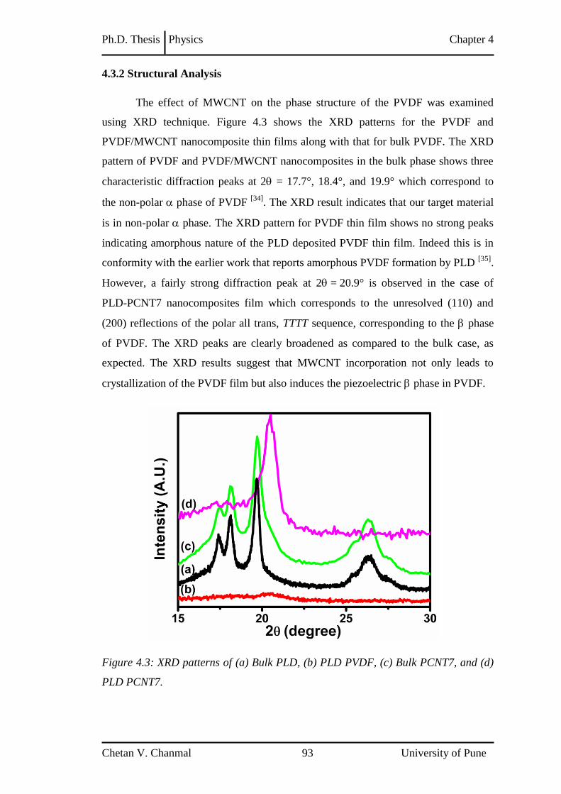
Ph.D. Thesis Physics Chapter 4
Chetan V. Chanmal 93 University of Pune
4.3.2 Structural Analysis
The effect of MWCNT on the phase structure of the PVDF was examined
using XRD technique. Figure 4.3 shows the XRD patterns for the PVDF and
PVDF/MWCNT nanocomposite thin films along with that for bulk PVDF. The XRD
pattern of PVDF and PVDF/MWCNT nanocomposites in the bulk phase shows three
characteristic diffraction peaks at 2 = 17.7°, 18.4°, and 19.9° which correspond to
the non-polar phase of PVDF [34]
. The XRD result indicates that our target material
is in non-polar phase. The XRD pattern for PVDF thin film shows no strong peaks
indicating amorphous nature of the PLD deposited PVDF thin film. Indeed this is in
conformity with the earlier work that reports amorphous PVDF formation by PLD [35]
.
However, a fairly strong diffraction peak at 2 = 20.9° is observed in the case of
PLD-PCNT7 nanocomposites film which corresponds to the unresolved (110) and
(200) reflections of the polar all trans, TTTT sequence, corresponding to the phase
of PVDF. The XRD peaks are clearly broadened as compared to the bulk case, as
expected. The XRD results suggest that MWCNT incorporation not only leads to
crystallization of the PVDF film but also induces the piezoelectric phase in PVDF.
Figure 4.3: XRD patterns of (a) Bulk PLD, (b) PLD PVDF, (c) Bulk PCNT7, and (d)
PLD PCNT7.
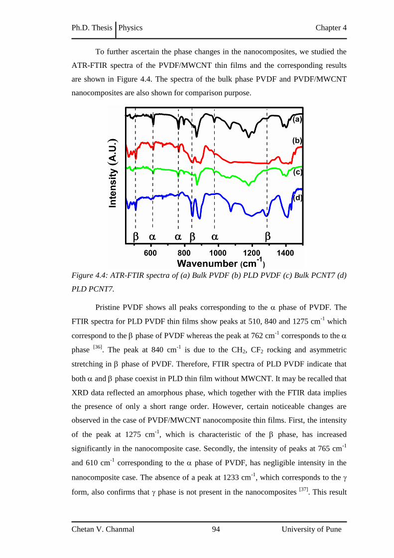
Ph.D. Thesis Physics Chapter 4
Chetan V. Chanmal 94 University of Pune
To further ascertain the phase changes in the nanocomposites, we studied the
ATR-FTIR spectra of the PVDF/MWCNT thin films and the corresponding results
are shown in Figure 4.4. The spectra of the bulk phase PVDF and PVDF/MWCNT
nanocomposites are also shown for comparison purpose.
Figure 4.4: ATR-FTIR spectra of (a) Bulk PVDF (b) PLD PVDF (c) Bulk PCNT7 (d)
PLD PCNT7.
Pristine PVDF shows all peaks corresponding to the phase of PVDF. The
FTIR spectra for PLD PVDF thin films show peaks at 510, 840 and 1275 cm-1
which
correspond to the phase of PVDF whereas the peak at 762 cm-1
corresponds to the
phase [36]
. The peak at 840 cm-1
is due to the CH2, CF2 rocking and asymmetric
stretching in phase of PVDF. Therefore, FTIR spectra of PLD PVDF indicate that
both and phase coexist in PLD thin film without MWCNT. It may be recalled that
XRD data reflected an amorphous phase, which together with the FTIR data implies
the presence of only a short range order. However, certain noticeable changes are
observed in the case of PVDF/MWCNT nanocomposite thin films. First, the intensity
of the peak at 1275 cm-1
, which is characteristic of the phase, has increased
significantly in the nanocomposite case. Secondly, the intensity of peaks at 765 cm-1
and 610 cm-1
corresponding to the phase of PVDF, has negligible intensity in the
nanocomposite case. The absence of a peak at 1233 cm-1
, which corresponds to the
form, also confirms that phase is not present in the nanocomposites [37]
. This result
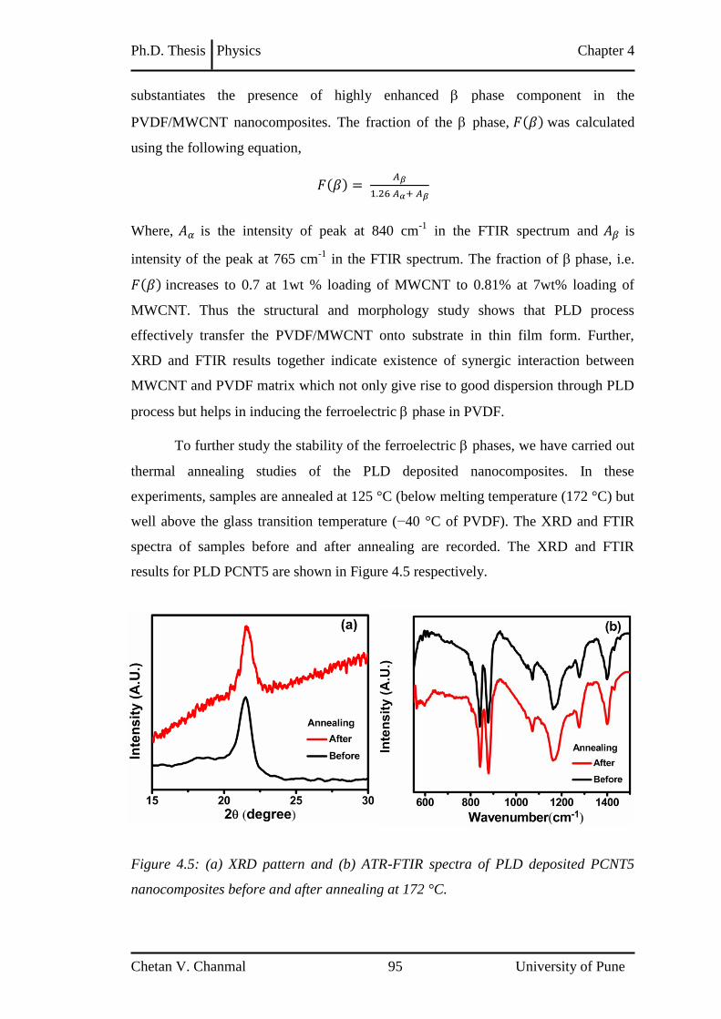
Ph.D. Thesis Physics Chapter 4
Chetan V. Chanmal 95 University of Pune
substantiates the presence of highly enhanced phase component in the
PVDF/MWCNT nanocomposites. The fraction of the phase, was calculated
using the following equation,
Where, is the intensity of peak at 840 cm-1
in the FTIR spectrum and is
intensity of the peak at 765 cm-1
in the FTIR spectrum. The fraction of phase, i.e.
increases to 0.7 at 1wt % loading of MWCNT to 0.81% at 7wt% loading of
MWCNT. Thus the structural and morphology study shows that PLD process
effectively transfer the PVDF/MWCNT onto substrate in thin film form. Further,
XRD and FTIR results together indicate existence of synergic interaction between
MWCNT and PVDF matrix which not only give rise to good dispersion through PLD
process but helps in inducing the ferroelectric phase in PVDF.
To further study the stability of the ferroelectric phases, we have carried out
thermal annealing studies of the PLD deposited nanocomposites. In these
experiments, samples are annealed at 125 °C (below melting temperature (172 °C) but
well above the glass transition temperature (−40 °C of PVDF). The XRD and FTIR
spectra of samples before and after annealing are recorded. The XRD and FTIR
results for PLD PCNT5 are shown in Figure 4.5 respectively.
Figure 4.5: (a) XRD pattern and (b) ATR-FTIR spectra of PLD deposited PCNT5
nanocomposites before and after annealing at 172 °C.

Ph.D. Thesis Physics Chapter 4
Chetan V. Chanmal 96 University of Pune
The results of XRD and FTIR indicate that the characteristic peak positions for PLD
deposited samples remain unaffected before and after annealing. This confirms that
the crystalline phases are stable in the nanocomposites.
Raman Spectroscopy
Raman spectroscopy is a very sensitive tool to study the possible interactions
between polymer and the MWCNT. Raman spectra of nanocomposites thin films
along with pristine MWCNT were shown in Figure 4.6. The Raman spectra of both
pure MWCNT and thin films of PVDF/MWCNT are similar indicating that PLD does
not affects the basic structure of MWCNT. The Raman spectra show two bands at
1350 cm-1
(D-band) and 1580 cm-1
(G- band). The D band is associated with the
disordered or amorphous carbon material while the G band is associated with the in-
plane vibration of the sp2-bonded carbon atoms. The peak intensity of D-band is
higher than G-band which indicates great deal of amorphous carbon and impurities in
the pure MWCNT. In PVDF/MWNT thin films, G-band is slightly red shifted towards
higher wave number indicating interfacial interaction between MWCNT and PVDF
nanocomposites [38]
. The ratio of intensity of D-band to G-band is normally used to
express the amount of graphitization in carbon nanotubes. In thin film
PVDF/MWCNT nanocomposite films the ratio is decreased from 1.40 to 1.14. The
reduction in the intensity ratio of Id/Ig indicates that amorphous carbon material has
been removed and the graphitization content of CNT has been increased during PLD
process.
Figure 4.6: Raman spectra of (a) pristine MWCNT and PLD films of (b) PCNT1 (c)
PCNT3 (d) PCNT5 and (e) PCNT7 nanocomposites.

Ph.D. Thesis Physics Chapter 4
Chetan V. Chanmal 97 University of Pune
4.3.3 TEM Analysis
The high resolution transmission electron microscopy (HRTEM) images of
pristine MWCNT and MWCNT embedded in the PVDF matrix as obtained by the
PLD process are shown in Figure 4.7. To obtain the latter the film was directly
deposited on the TEM grid.
Figure 4.7: HRTEM images of (a) & (b) Pristine MWCNT and (c) & (d) PLD
deposited PCNT5 nanocomposite.
The TEM morphology of pure MWCNT shows that the tubes are randomly
coiled and the tube ends are not visible over the observation area whereas the tube
ends are clearly visible in the case of PLD-PCNT5 nanocomposite film. Thus the
HRTEM images confirm that the basic nature of MWCNT remain intact in the PLD
process. However, the presence of tube ends indicates the possible breakage of
MWCNTs in the PLD process which results decrease in the aspect ratio of MWCNT.
It is well known that in case of MWCNT polymer nanocomposites lower aspect ratio
gives rise to higher percolation threshold [39]
.
(B) (a) (b)
(c) (d)

Ph.D. Thesis Physics Chapter 4
Chetan V. Chanmal 98 University of Pune
4.3.4 Dielectric Relaxation Spectroscopy (DRS)
The dielectric properties of nanocomposites were examined by fabricating a
capacitor type of configuration. The PVDF/MWCNT thin films were deposited on
copper substrate which also serves as a bottom electrode and the top contact is
provided with platinum. The thickness of the film was measured using profilometer
and used in the measurement of the dielectric permittivity. Figure 4.8 shows the
frequency dependence of dielectric permittivity for different loading of MWCNT. The
dielectric permittivity shows a composition dependent systematic increase in
permittivity over the entire frequency range. The permittivity variation of
PVDF/MWCNT nanocomposite films shows a behavior characteristically similar to
PVDF. However, as compared to pristine PVDF, the dielectric permittivity for
PCNT7 nanocomposite increases to about 560 at a frequency of 10+02
Hz. Importantly,
dielectric permittivity of PVDF/MWCNT nanocomposite film is found to be almost
independent of frequency for each composition. The observed increase in the
dielectric permittivity can be ascribed to either Maxwell-Wagner-Sillars (MWS)
polarization or formation of large number of minicapacitors network in
nanocomposites [33, 40]
. In the case of MWS polarization, charges are trapped at the
interface having material with different relaxation time ( =/) arising due to
difference in the dielectric permittivity and conductivity [40, 41].
This leads to enormous
increase in the permittivity and strong dependence of dielectric permittivity in the low
frequency region. However, in the present case the possibility of MWS polarization
can be neglected due to the frequency independent nature of dielectric permittivity. It
is well reported that the distribution of MWCNT within the insulating polymer matrix
forms lots of minicapacitors connected in series and parallel combinations [42]
.
Initially, when low amount of MWCNT is added into PVDF matrix, some
minicapacitors are formed resulting into slight increase in the dielectric permittivity.
With the increasing loading of MWCNT, the dielectric permittivity gradually
increases. As the percolation threshold approaches, there are many conducting
MWCNTs wrapped with the thin layer of insulating polymer matrix forming lots of
minicapacitors network. This minicapacitor network formation significantly improves
the dielectric permittivity of the nanocomposites [43-45].
Thus, in the present case the
significant increase in the dielectric permittivity of the PVDF/MWCNT
nanocomposites can be mainly attributed to the homogenous distribution of MWCNT

Ph.D. Thesis Physics Chapter 4
Chetan V. Chanmal 99 University of Pune
in the PVDF matrix and gradual formation of large number of mini-capacitor network
as the MWCNT content increases.
Figure 4.8: Dielectric permittivity spectra of PLD deposited PVDF and
PVDF/MWCNT nanocomposites.
Figure 4.9 presents the dielectric loss (tan ) as a function of frequency for
PVDF/MWCNT nanocomposites with different loading of MWCNT. The dielectric
loss spectrum shows broad relaxation around 1 × 10⁷ Hz which corresponds to the
glass transition relaxation of PVDF. The high frequency limit of the instrument
constrains the full view of glass transition relaxation. From the figure 4.9 it can be
also seen that dielectric loss increases with increasing filler loading. For lower loading
of MWCNT, the dielectric loss spectrum is similar to PVDF and the dielectric loss
values are well below 0.4 over the entire frequency range. However, a dramatic
increase in the dielectric loss is observed for PCNT7 nanocomposite. The increase in
the dielectric loss may be due to the increase in the electrical conductivity of
nanocomposites which can be ascribed to the onset of percolation threshold in
nanocomposites [46]
. It has reported that, in the percolation region, the dielectric loss
increases significantly with increasing filler loading [8]
. The percolation threshold in
bulk phase PVDF/MWCNT nanocomposites is reported to be less than 1.6 vol%
loading of MWCNT [47]
. In our case the percolation threshold appears at about
5.9 vol% loading of MWCNT. In case of MWCNT based nanocomposites,
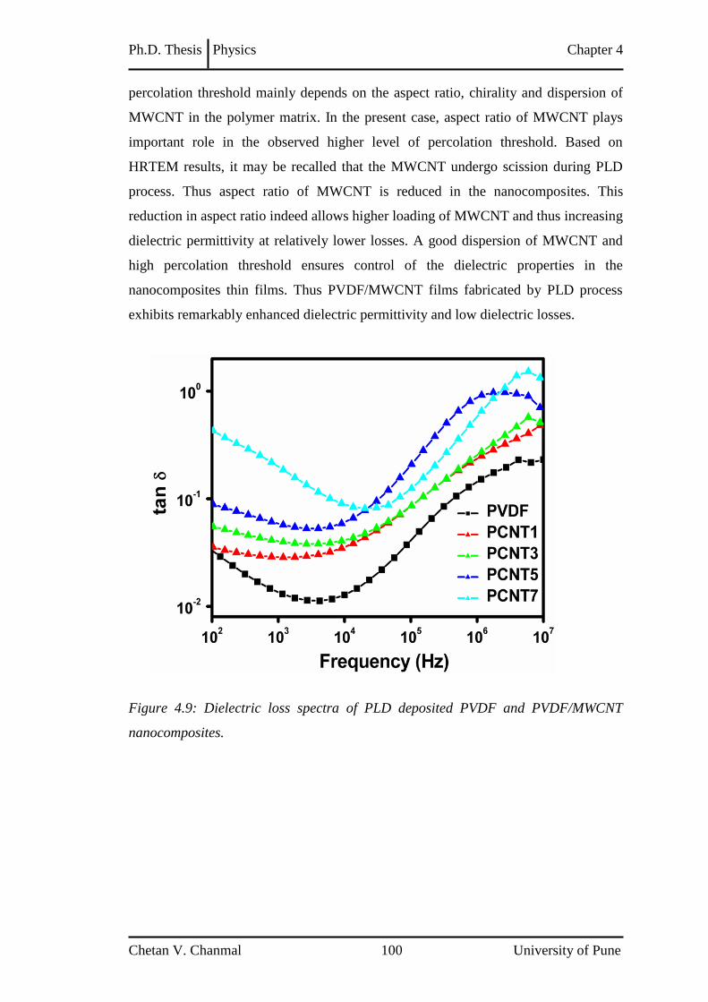
Ph.D. Thesis Physics Chapter 4
Chetan V. Chanmal 100 University of Pune
percolation threshold mainly depends on the aspect ratio, chirality and dispersion of
MWCNT in the polymer matrix. In the present case, aspect ratio of MWCNT plays
important role in the observed higher level of percolation threshold. Based on
HRTEM results, it may be recalled that the MWCNT undergo scission during PLD
process. Thus aspect ratio of MWCNT is reduced in the nanocomposites. This
reduction in aspect ratio indeed allows higher loading of MWCNT and thus increasing
dielectric permittivity at relatively lower losses. A good dispersion of MWCNT and
high percolation threshold ensures control of the dielectric properties in the
nanocomposites thin films. Thus PVDF/MWCNT films fabricated by PLD process
exhibits remarkably enhanced dielectric permittivity and low dielectric losses.
Figure 4.9: Dielectric loss spectra of PLD deposited PVDF and PVDF/MWCNT
nanocomposites.

Ph.D. Thesis Physics Chapter 4
Chetan V. Chanmal 101 University of Pune
4.3.5 AC Conductivity
Figure 4.10 shows the ac conductivity of PVDF/MWCNT nanocomposite
films as a function of frequency for different MWCNT loading.
Figure 4.10: ac conductivity spectra of PLD deposited PVDF and PVDF/MWCNT
nanocomposites at 10-01
Hz.
The ac conductivity spectra shows that conductivity increase with increasing
loading of MWCNT. For example at 10−01
Hz the conductivity is 1.5 × 10⁻¹⁵
S/cm for
PVDF which increases to 5.2 × 10−09
S/cm for PCNT7 nanocomposite. For lower
loading of MWCNT (up to PCNT3) conductivity of composites increases with
increasing frequency, this indicates that nanocomposites behave like electric
insulators. At this loading, MWCNTs do not form electrically conductive network and
they are still below the percolation threshold. However, with further increase in
MWCNT loading, the conductivity shows a tendency towards frequency independent
behavior in the low frequency regime indicating typical non-dielectric behavior.
Particularly for PCNT7 nanocomposite, a plateau or frequency independent
conductivity behavior over low frequency regime and frequency dependent
conductivity at higher frequencies is clearly observed. For PCNT7 conductivity
increases from 5.2 × 10−09
S/cm to 3.5 × 10−04
S/cm indicating occurrence of
percolation threshold.

Ph.D. Thesis Physics Chapter 4
Chetan V. Chanmal 102 University of Pune
The frequency dependence of the real part of the conductivity near the
percolation threshold is predicted to have a power-law form [48]
.
This behavior is generally explained by Jonscher’s Universal power law,
Where is the dc conductivity, A is the pre-exponential factor and n is the fractional
exponent between 0 and 1.This law introduces a critical frequency, fC , below which
the real part of conductivity is independent of frequency and identical to the dc
conductivity, the conductivity mechanism being termed as “diffusive”. Above fc, the
conductivity increases with increasing frequency, following the power law given
above, and leads to a frequency-dependent “subdiffusive” motion of mobile charges
[49]. Figure 4.11 shows that the experimental data for PCNT7 nanocomposite fits fairly
well to power law equation, and the value of the exponent about 0.8 which is close to
the normal value of percolation theory [50]
.
Figure 4.11: Power law fit to conductivity spectra of PLD PCNT7 nanocomposite.

Ph.D. Thesis Physics Chapter 4
Chetan V. Chanmal 103 University of Pune
Thus, the dielectric studies of PVDF/MWCNT nanocomposites shows that the
enhanced value of permittivity is achieved at relatively low dielectric loss and
moderate conductivity level. These results can be attributed to the increase in the
percolation threshold due to the lower aspect ratio of MWCNTs in the
nanocomposites [51]
. The possible breakage of MWCNTs obstructs the direct physical
contact between MWCNTs and therefore it is possible to have high filler loading
without reaching the percolation. The results also suggest that, the ferroelectric
phase and enhanced dielectric permittivity of PVDF/MWCNT nanocomposites can be
achieved without any chemical functionalization of MWCNTs. Additionally, the
fabrication of the nanocomposites into thin film phase, using PLD technique, gives an
excellent opportunity of exploring potential applications of nanocomposites in the
field micro-electromechanical systems.
Figure 4.12 shows the variation of dielectric permittivity and loss as a function
of filler loading at a frequency of 10+02
Hz.
Figure 4.12: Variation in the dielectric permittivity and tanas a function of
MWCNT loading at 10+02
Hz.
The dielectric permittivity is found to increase with increasing filler loading.
As can be seen from the figure, a remarkable increase in the dielectric permittivity is
observed for PCNT7 nanocomposites. The dielectric permittivity reaches to around
560 at this loading with loss of 0.4 and conductivity value of 3 × 10⁻⁸
S/cm, at
10+02
Hz.
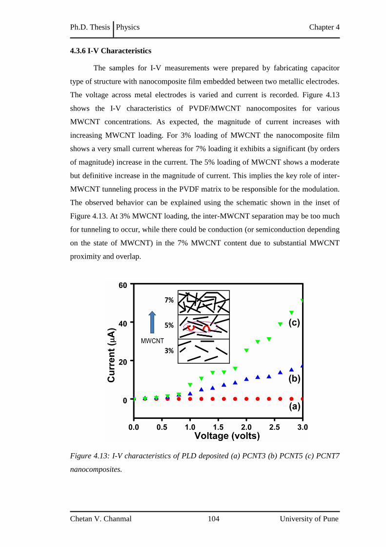
Ph.D. Thesis Physics Chapter 4
Chetan V. Chanmal 104 University of Pune
4.3.6 I-V Characteristics
The samples for I-V measurements were prepared by fabricating capacitor
type of structure with nanocomposite film embedded between two metallic electrodes.
The voltage across metal electrodes is varied and current is recorded. Figure 4.13
shows the I-V characteristics of PVDF/MWCNT nanocomposites for various
MWCNT concentrations. As expected, the magnitude of current increases with
increasing MWCNT loading. For 3% loading of MWCNT the nanocomposite film
shows a very small current whereas for 7% loading it exhibits a significant (by orders
of magnitude) increase in the current. The 5% loading of MWCNT shows a moderate
but definitive increase in the magnitude of current. This implies the key role of inter-
MWCNT tunneling process in the PVDF matrix to be responsible for the modulation.
The observed behavior can be explained using the schematic shown in the inset of
Figure 4.13. At 3% MWCNT loading, the inter-MWCNT separation may be too much
for tunneling to occur, while there could be conduction (or semiconduction depending
on the state of MWCNT) in the 7% MWCNT content due to substantial MWCNT
proximity and overlap.
Figure 4.13: I-V characteristics of PLD deposited (a) PCNT3 (b) PCNT5 (c) PCNT7
nanocomposites.

Ph.D. Thesis Physics Chapter 4
Chetan V. Chanmal 105 University of Pune
4.3.7 Scanning Tunneling Microscopy (STM)
Scanning tunneling microscopy is important tool to study the electronic
properties of materials at atomic resolution. Before discussing the corresponding
device fabrication and testing, we present data on scanning tunneling microscopy and
spectroscopy (STM/STS) to examine the channel in electrical terms.
The interesting MWCNT loading dependent dielectric / electrical properties of
PLD PCNT5 thin films obtained in the present work were clearly judged to be
promising for use as an active channel material in field-effect transistor devices.
Figure 4.14(a) show the I-V curves acquired at distinct 64 equally spaced points in a
scan area of 500nm × 500nm and the corresponding STM image is shown in the inset.
Interestingly, all I-V curves at different points are fairly close to one another implying
a fair degree of electrical homogeneity in this nanocomposite film.
Figure 4.14: (a) I-V curves of PLD-PCNT5 thin films at 64 distinct locations obtained
from STM. Inset shows the STM image with blue dots showing locations of I-V
measurement (b) Localized Density of states (DOS) of PLD-PCNT5 determined from
STM.
In STM, current I is recorded as a function of bias voltage V applied to the
sample. The differential conductance (dI/dV) can then considered to be proportional
to the Density of states (DOS) of the sample examined. Normally on semiconductor
samples, (dI/dV)/(I/V) is used to represent the DOS rather than the direct derivative
dI/dV which is called normalization. This also accounts for the voltage dependence of
the tunnel barrier at high bias. The spatial averaged density of states (DOS) shown in

Ph.D. Thesis Physics Chapter 4
Chetan V. Chanmal 106 University of Pune
figure 4.14 (b) was calculated numerically from the I-V curves. The DOS data give a
gap ( = V+ − V-) of ~ 1.8 eV that closely matches with the gap value extracted from
STM/STS techniques on single SWCNT [52, 53].
However, the gap on PVDF/MWCNT
is not very sharp as seen in single CNTs and shows a band tailing in the unoccupied
states, which could possibly suggest interface states at the CNT/polymer interface.
4.3.8 Field Effect Device using Nanocomposites Channel Layer
From the I-V Characteristics (shown in figure 4.13), it is clear that 5 wt%
loading of MWCNT shows the moderate increase in the current. On the other hand, 3
wt% loading shows no appreciable increase in the current and 7% loading shows large
increase in the current value. When the nanocomposites was used as a channel layer
in field effect device, we observed that only 5% loading shows the effective
modulation in the drain current whereas the 3% and 7 % loading shows less or no
modulation in the current. This can be related to the conductivity level at different
loading of MWCNTs. The critical level of conductivity and non-percolative network
of MWCNTs at 5% loading was responsible for this observation.
The device was fabricated with PCNT5 nanocomposite as an active channel
layer. The output and transfer characteristics of the PCNT5-FET are shown in Fig.
4.15 (a) and Fig. 4.15 (b), respectively. The results clearly show that the gate voltage
of 4V can modulate the source-drain current by almost more than two orders of
magnitude with ON/OFF ratio of around 32. In the basic IDS-VDS characteristic the
drain current (IDS) increases non-linearly with the source-drain voltage, a behavior
similar to that reported in single CNT based devices [54-57].
This non-linearity in I-V
characteristics is generally observed in field effect devices and has been attributed to
the space charge limited current (SCLC) and electrode effects [58, 59]
. In output
characteristics, application of a negative gate bias (which injects holes) enhances IDS,
while a positive gate bias (electron injection) suppresses it. For negative gate bias,
holes are accumulated at semiconductor and dielectric interface leading to an increase
in the conductance, whereas for positive bias holes are depleted and conductance
decreases. This implies that the majority carriers in our channel layer are holes. This
can also be seen from the transfer characteristics of the device measured at VDS= 5V
and 10V wherein at a given VDS, IDS decreases with increasing gate voltage (VG), a
sign of a p-type material [60, 61]
.

Ph.D. Thesis Physics Chapter 4
Chetan V. Chanmal 107 University of Pune
Figure 4.15: (a) Output Characteristics and (b) transfer characteristics of PCNT5
nanocomposites FET device.
A non-percolating network of nanotubes embedded in the PVDF matrix
represents an interesting and unique channel layer in many ways in so far as an FET
device action is concerned. A schematic of such assembly in an FET configuration is
shown in inset of Figure 4.16. The intertwined yet electronically separated conducting
or semiconducting nanotubes provide the transport channel within the PVDF matrix.
The external field applied at electrodes is responsible for the injection of charge
carriers in the channel and the inter-MWCNT tunneling process in the PVDF matrix
(with enhanced piezoelectric -phase contribution) are responsible for observed
modulation.
Figure 4.16: Schematic showing of FET device action in PVDF/MWCNT
nanocomposite as a channel layer.
Ph.D. Thesis Physics Chapter 4
Chetan V. Chanmal 108 University of Pune
4.4 Conclusions
In conclusion, we have fabricated thin films of PVDF/MWCNT
nanocomposite by pulsed laser deposition. Interestingly the addition of MWCNTs
renders crystallinity to the polymeric film and also induces the ferroelectric phase of
PVDF. The dielectric permittivity of nanocomposites increases with increasing
loading of MWCNT at relatively low dielectric losses. The enhanced dielectric
permittivity was explained on the basis of formation minicapacitor network in
nanocomposites. The control over the dielectric properties obtained through higher
percolation threshold offers use of these nanocomposites in various applications. The
fabricated PVDF/MWCNT nanocomposite films were used in an electric field
modulation device. When used as a channel layer in a field effect transistor
configuration, a strong electric field modulation of the transport was realized just
below the percolation threshold. The nanocomposite film with MWCNT content just
below the percolation threshold shows strong modulation of drain current with gate
voltage. The output and transfer characteristics show that the PVDF/MWCNT
nanocomposite channel exhibits p-type behavior. We believe that, the idea of the use
of nanocomposite non-percolating channel concept can provide several opportunities
for FET devices for organic electronics.
4.5 References
1. L. Qi, B. I. Lee, S. Chen, W. D. Samuels, G. J. Exarhos, Adv. Mater., 2005, 17,
1777-1781.
2. P. Kim, N. M. Doss, J. P. Tillotson, P. J. Hotchkiss, M. J. Pan, S. R. Marder, J.
Li, J. P. Calame, J. W. Perry, ACS Nano, 2009, 3, 2581-2592.
3. S. Han, X. liu, J.P. Han, C. Zhou, Appl. Phys. A, 2003, 77, 873–875.
4. C. V. Chanmal, J.P. Jog, eXpress polymer letters, 2008, 2, 294-301.
5. P.Kim, N.M. Doss, J.P.Tillotson, P. J. Hotchkiss, M.J.Pan, S.R. Marder, J. Li,
J.P. Calame, J.W. Perry, ACS Nano, 2009, 3, 2581-2592.
6. Maheswar Panda, V. Srinivas, A. K. Thakur, Appl. Phys. Lett., 2008, 93,
242908.
7. Yun-Jia Li, Man Xu, Jun-Qiang Feng, Zhi-Min Dang, Appl. Phys. Lett., 2006,
89, 072902.
8. C.W. Nan, Y. Shen, Jing Ma, Annu. Rev. Mater. Res., 2010, 40, 131–151.

Ph.D. Thesis Physics Chapter 4
Chetan V. Chanmal 109 University of Pune
9. Michele T. Byrne, Yurii K. Gun’ko, Adv. Mater., 2010, 22, 1672–1688.
10. S. Manna, A. K. Nandi, J. Phys. Chem. C., 2007, 111, 14670-14680.
11. Z.M. Dang, S. H. Yao, H. P. Xu, Appl. Phys. Lett., 2007, 90,012907.
12. R. H. Schmidt, I. A. Kinloch, A. N. Burgess, A. H. Windle, Langmuir, 2007, 23,
5707-5712.
13. D. Chen, M. Wang, W.D. Zhang, T. Liu, J. Applied Polymer Science, 2009, 113,
644-650.
14. D.B.Chrisey, A. Pique, R.A. McGill, J.S. Horwitz, B.R. Ringeisen, D.M. Bubb,
P.K.Wu, Chem. Rev., 2003, 103, 553-576.
15. J. Faupel, C. Fuhse, A. Meschede, C. Herweg, H.U. Krebs, S. Vitta, Appl. Phys.
A, 2004, 79, 1233-1235.
16. R. Gregorio Jr., M. Cestari, J. Polym. Sci.: Part B: Polym. Phys., 1994, 32, 859-
870.
17. A. J. Lovinger, Science, 1983, 220, 1115–1121.
18. L. Priya, J.P. Jog, J. Polym. Sci.: Part B: Polym. Phys., 2002, 40, 1682-1689.
19. R. P. Vijayakumar, D. V. Khakhar, A. Misra, J. Appl. Polym. Sci., 2010, 117,
3491-3497.
20. S. L. Hsu, F. J. Lu, D. A. Waldman, M. Muthukumar, Macromolecules, 1985,
18, 2583-2587.
21. V. Sencadas, S. L. Mendez, J. F. Mano, Thermochimica Acta, 2004, 424, 201–
207.
22. S. Yu, W. Zheng, W. Yu, Y. Zhang, Q. Jiang, Z. Zhao, Macromolecules, 2009,
42, 8870-8874.
23. S. Huang, W.A. Yee, W.C. Tjiu, Y. Liu, M. Kotaki, Y.C.F. Boey, J. Ma, T. Liu,
X.Lu, Langmuir, 2008, 24, 13621-13626.
24. M. Muccini, Nature Mater., 2006, 5, 605.
25. E. Menard, V. Podzorov, S.H. Hur, A. Gaur, M.E. Gershenson, J.A. Ogers, Adv.
Mater., 2004, 16, 2097.
26. S. B. Ogale, V. Talyansky, C. H. Chen, R. Ramesh, R. L. Greene, T. Venkatesan,
Phys. Rev. Lett., 1996, 77 1159.
27. Q. Cao, J.A. Rogers, Adv. Mater., 2009, 21, 29.
28. Q. Cao, S. Hur, Z. Zhu, Y. Sun, C. Wang, M.A. Meitl, M. Shim, J.A. Rogers,
Adv. Mater., 2006, 18, 304.

Ph.D. Thesis Physics Chapter 4
Chetan V. Chanmal 110 University of Pune
29. C.F. Sung, D. Kekuda, L.F. Chu, Y.Z. Lee, F.C. Chen, M.C. Wu, C.W. Chu,
Adv. Mater., 2009, 21, 1.
30. R.T. Weitz, U.Zchieschang, F. Effenberger, H. Klauk, M.Burghard, K.Kern,
Nano Lett., 2007, 7, 22.
31. G. Eda , M.Chhowalla, Nano lett., 2009, 9, 814.
32. Y. Jang, W.H. Lee, Y.D. Park, D. Kwak, J.H. Cho, K. Cho, Appl. Phys. Lett.,
2009, 94, 183301.
33. Q. Chen, P. Du, L. Jin, W. Weng, G. Han, Appl. Phys. Lett., 2007, 91, 022912.
34. W.A. Yee, M. Kotaki, Y. Liu, X. Lu, Polymer, 2007, 48, 512-521.
35. M.G. Norton, W. Jiang, J. T. Dickinson, K.W. Hipps, Appl. Surf. Sci., 1996, 96,
617-620.
36. M. Kobayashi, K. Tashiro, H. Tadokoro, Macromolecules, 1975, 8, 158-171.
37. M.Benz, W.B.Euler, J. App. Polym.Sci., 2003, 89, 1093-1100.
38. Guang Xin Chen, Yongjin Li, Hiroshi Shimizu, Carbon, 2007, 45, 2334-2340.
39. S.H. Yao, Z.M. Dang, M.J. Jiang, H.P. Xu, J. Bai, Appl. Phys. Lett., 2007, 91,
212901.
40. F. He, S. Lau, H. L. Chan, J. Fan, Adv. Mater., 2009, 21, 710-715.
41. R. Tamura, E. Lim, T. Manaka, M. Iwamoto, J. Appl. Phys., 2006, 100, 114515.
42. Qun Li, Qingzhong Xue, Lanzhong Hao, Xili Gao, Qingbin Zheng, Composites
Science and Technology, 2008, 68, 2290–2296.
43. R. Simoes, J. Silva, R. Vaia, V. Sencadas, P. Costa, J. Gomes, S. L. Mendez,
Nanotechnology, 2009, 20, 035703.
44. S. H. Yao, Z.M. Dang, H.P. Xu, M.J. Jiang, J. Bai, Appl. Phys. Lett., 2008, 92,
082902.
45. J.K. Yuan, S.H. Yao, Z.M. Dang, A. Sylvestre, M. Genestoux, J Bai, J. Phys.
Chem. C., 2011, 115, 5515-5521.
46. Z.M. Dang, L. Wang, V. Yin, Q. Zhang, Q. Lei, Adv. Mater., 2007, 19, 852-857.
47. L. Wang, Z.M. Dang, Appl. Phys. Lett., 2005, 87, 042903.
48. A. Linares, J. C. Canalda, M. E. Cagiao, M. C. G. Gutierrez, A. Nogales, I. M.
Gullon, J. Vera, T. A. Ezquerra, Macromolecules, 2008, 41, 7090-7097.
49. B. Roling, Dielectrics Newsletter, 2002, Issue 17, 1.
50. Jin-Kai Yuan, Zhi-Min Dang, Sheng-Hong Yao, Jun-Wei Zha, Tao Zhou,
Sheng-Tao Lib and Jinbo Bai, J. Mater. Chem., 2010, 20, 2441–2447.
Ph.D. Thesis Physics Chapter 4
Chetan V. Chanmal 111 University of Pune
51. P. Costa, J. Silva, V. Sencadas, C. M. Costa, F. W. J. hattum, J. G. Rocha, S.L.
Mendez, Carbon, 2009, 47, 2590-2599.
52. J.W.G. Wildoer, L.C. Venema, A.G. Rinzler, R.E. Smalley, C. Dekker, Nature,
1998, 391, 59.
53. T. W. Odom, J. Huang, P.Kim, C.M. Lieber, Nature, 1998, 391, 62.
54. J. Vaillancourt, H. Zhang, P. Vasinajindakaw, H. Xia, X. Lu, X. Han, D. C.
Janzen, W.S. Shih, C.S. Jones, M. Stroder, M. Y. Chen, H. Subbaraman, R. T.
Chen, U. Berger, M. Renn, Appl. Phys. Lett., 2008, 93, 243301.
55. S.J. Tans, A. Verschueren, C. Dekker, Nature, 1998, 393, 49.
56. K. Maehashi, T. Katsura, K. Kerman, Y. Takamura, K. Matsumoto, E. Tamiya,
Anal. Chem., 2007, 79, 782.
57. E. G. Espino, G. Sala, F. Pino, N. Halonen, J. Luomahaara, J, Maklin, G. Toth,
K. Kordas, H. Jantunen, M. Terrones, P. Helisto, H. Seppa, P.M. Ajayan, R.
Vajtai, Nano, 2010, 6 ,3318.
58. T. Hirose, T. Nagase, T. Kobayashi, R. Ueda, A. Otomo, H. Naito, Appl. Phys.
Lett., 2010, 97, 083301.
59. T. Hou, J. Han, T. Yamda, P. Nguyen, Y. P. Chen, M. Meyyappan, Nano Lett.,
2004, 4 1247.
60. E. Artukovic, M. Kaempgen, D.S. Hecht, S. Roth, G. Gruner, Nano Lett., 2005,
5, 75.
61. J. Zhang, P.C. Chen, G. Shen, J. He, A. Kumbhar, C. Zhou, J. Fang, Angew.
Chem. Int. Ed., 2008, 47, 9469.

Chetan V. Chanmal 112 University of Pune
Chapter 5
Nonvolatile Memory and
Infrared (IR) Sensor based on PVDF/Clay
Nanocomposites
This chapter presents the dielectric characterization of PVDF/Clay nanocomposites
and demonstrate its application as a gate dielectric material in field effect transistor.
The nanocomposites exhibit significant enhancement in the dielectric permittivity
which is attributed to the strong interfacial interaction between polymer matrix and
clay platelets. The nanocomposite material was directly integrated in FET device
architecture. The nanocomposite gate dielectric FET shows excellent transistor
performance along with excellent memory retention characteristics and infrared (IR)
sensing capability due to the ferroelectric and pyroelectric properties of gate
dielectric.
Part of the work presented in this chapter has been published in following
journals:
1. C. V. Chanmal, J. P. Jog, e-Polymers,2009, no. 112.

Ph.D. Thesis Physics Chapter 5
Chetan V. Chanmal 113 University of Pune
Section I: Dielectric Studies of PVDF/Clay Nanocomposites
5.I.1 Introduction
Electroactive polymers play an important role in many fields like micro-
electronic-mechanical systems (MEMs), gate dielectric material, embedded capacitor
application and energy storage. For such applications, materials with high electric
energy storage density are required which can be achieved by increasing the dielectric
permittivity of material [1]
.
Polymer based nanocomposite materials with high
dielectric permittivity were been studied extensively as a potential candidate for such
applications [2-4].
The most popular approach to increase the dielectric permittivity of
the polymer is by incorporating inorganic ferroelectric metal oxides such as Lead
Zirconium Titanate (PZT), Barium Titanate (BaTiO3) etc. [5-7]
. However, a very high
loading up to 50% by volume were generally required to achieve desired enhancement
in permittivity. Also, the large difference between the two phases can give rise to
highly inhomogenous electric fields. Till date, nanofillers such as BaTiO3 and
multiwalled carbon nanotubes (MWCNT) are reported to result in improved dielectric
permittivity without compromising the flexibility of the polymer [8, 9]
. Another
approach which recently gained significant research interest is the effect of clay
addition on the dielectric properties of polymer. Polymer clay nanocomposites
represent a new class of materials based on reinforcement of polymer chain by
dispersion of nano-scale clay particles [10]
. Thus from fundamental point of view,
polymer/clay nanocomposites serve as model systems to study the confinement effect
on various properties of polymers [11]
. Dielectric spectroscopy is indeed found to be an
excellent tool to understand the confinement effects in these systems.
In this chapter we discuss the effect of different content of clay on the
dielectric permittivity and relaxation dynamics of PVDF. As reported by Priya and
Jog, it was observed that presence of clay transforms the PVDF into ferroelectric
phase [12]
. They observed that melt processing of PVDF/clay nanocomposites results
into the formation of phase instead of phase. It was suggested that, the close
matching of crystal lattice of clay with that of the phase of PVDF is probably
responsible for the crystallization and stabilization of phase. The earlier studies on
PVDF/Clay nanocomposites showed increase in the melting temperature (6 °C to
8 °C) and crystallization (10 °C to 12 °C) temperature of PVDF. The storage modulus

Ph.D. Thesis Physics Chapter 5
Chetan V. Chanmal 114 University of Pune
was also found to increase significantly with the addition of clay. In this context it is
interesting to study the effect of clay on the dielectric properties of PVDF.
5.I.2 Experimental
5.I.2.1 Materials and Processing of Nanocomposites
Polyvinylidene fluoride (PVDF) grade Solef 1008, supplied by Solvay
(Belgium) is used for the present study. The organically modified bentonite clay
sample used in the present study is Cloisite 20A procured from southern clay products
(United States). Nanocomposites of PVDF with 20A were prepared with 1.5, 3, 5, 7,
and 10% of clay loading on twin-screw extruder. The films of polymer/clay
nanocomposites for dielectric spectroscopy analysis were prepared by compression
molding at a temperature of 200 °C using Carver press model F-15181.
5.I.2.2 Nanocomposite Characterization
X-ray diffraction (XRD)
The structure of PVDF/Clay nanocomposite is investigated using Rigaku X-
ray diffractometer with Cu K1 (=0.154nm) radiation operated at 40 kV and 150 mA.
The samples are scanned in the 2 range of 10 to 60 degrees with scan rate at 4
degrees per minute.
Dielectric Relaxation Spectroscopy (DRS)
Dielectric measurements of PVDF and PVDF/clay nanocomposites were
carried out over broad frequency range (i.e.1 10−02
- 2 10+07
Hz) at different
constant temperatures using Novocontrol broadband dielectric spectrometer equipped
with ZGS active sample cell. The temperature sweep is carried out in the range of
30 °C to 150 °C by placing sample between two 20 mm gold plated electrodes. The
sample temperature was stable within less than ±0.1 °K. Quick drying silver paste is
used to ensure good electrical contact.
Scanning Electron microscopy (SEM)
The morphology of thin films was studied on Leica-440 Scanning Electron
Microscopy (SEM). Thin layer of gold was sputtered on the samples to avoid
charging effects.

Ph.D. Thesis Physics Chapter 5
Chetan V. Chanmal 115 University of Pune
5.I.3 Results and Discussion
5.I.3.1 Structural Analysis
Figure 5.1 (a) shows XRD results of PVDF/Clay nanocomposites. The XRD
pattern of pristine PVDF shows characteristic peaks at 18.1°, 18.7°, 20.1° and 26.8°
which corresponds to the (100), (020), (110), and (021) ofphase PVDF [13]
. On the
other hand, for PVDF/clay nanocomposites only a single peak at 20.6° corresponding
to the (110) / (200) planes of phase crystallization of PVDF can be observed. The
XRD pattern for 1.5 wt% of clay content shows a shoulder of phase PVDF with
strong peak of phase. With increasing content of clay increases the content while
depressing the phase substantially. Moreover, the full width at half maximum of
characteristic peaks increases with increasing clay loading which indicates the
decrease in crystallite size with clay loading. Thus, XRD analysis clearly reveals the
enhancement of phase PVDF in nanocomposites. Figure 5.1 (b) shows FTIR spectra
of PVDF/Clay nanocomposites. The FTIR spectra also show the phase enhancement
in nanocomposites.
Figure 5.1: (a) XRD and (b) ATR-FTIR pattern of PVDF and PVDF/Clay
nanocomposites.
The fraction of the phase, was calculated using the following equation,
Where, is the intensity of peak at 840 cm-1
in the FTIR spectrum and is
intensity of the peak at 765 cm-1
in the FTIR spectrum. The fraction of phase,
i.e. , for different clay loading is presented in table 5.1.
(a)

Ph.D. Thesis Physics Chapter 5
Chetan V. Chanmal 116 University of Pune
Sample Clay content (%) F()
PVDF 0 0.03
PVDF/Clay-1.5% 1.5 0.84
PVDF/Clay-5% 5 0.85
PVDF/Clay-7% 7 0.88
PVDF/Clay-10% 10 0.90
Table 5.1: Fraction of phase i.e. F() for PVDF and PVDF/Clay nanocomposites.
5.I.3.2 Dielectric Studies
Figure 5.2 shows a plot of frequency dependence of dielectric permittivity (')
for PVDF/Clay nanocomposites at 30 °C. The dielectric permittivity increases with
increasing clay loading over the entire frequency range of measurement. For example,
the dielectric permittivity at a frequency of 10−02
Hz increased from 12 for pristine
PVDF to about 165 for 10% clay content in the nanocomposites. The dielectric
permittivity at lower frequency is always greater than the higher frequency, which
indicates the higher electric polarization at lower frequency, because at lower
frequency dipoles get enough time to get oriented in the direction of applied field. The
increase in the permittivity with increasing clay loading, particularly in the low
frequency region, can be attributed to the interfacial polarization operative in low
frequency end of spectrum. In polymers and composites, interfacial polarization is
present due to the difference in the permittivity values of the filler and polymer matrix
and such interface can lead to increase in dielectric permittivity, particularly in low
frequency region.
Figure 5.2: Frequency dependence of dielectric permittivity (ε') curves for PVDF and
PVDF/clay nanocomposites.
Ph.D. Thesis Physics Chapter 5
Chetan V. Chanmal 117 University of Pune
The dielectric permittivity of the composites can be predicted using
logarithmic model based on effective medium theory [14-16]
. According to the
logarithmic model, effective dielectric permittivity of the composite can be calculated
by using the following equation,
This model predicts that in the absence of interfacial polarization, the
dielectric permittivity of composites ('composite) is linearly proportional to volume
fraction of filler (filler) [17, 18]
. The dielectric permittivity of organically modified clay
pellet is measured over the frequency range and the value of dielectric permittivity
(40000) at a frequency of 0.01 Hz is used for the calculations. Figure 5.3 compares
the dielectric permittivity PVDF/clay nanocomposites as a function of clay loading at
0.01 Hz. As shown in figure 5.3, the calculated values of permittivity using the
logarithmic model increased from 12 (for PVDF) to 20 (for 10 wt% of clay loading)
in PVDF/clay nanocomposites. However, the experimental values of the dielectric
permittivity in PVDF/clay nanocomposites are found to increase from 12 (for PVDF)
to 165 (for 10 wt% of clay loading). This result indicates that PVDF/clay
nanocomposites does not obey simple logarithmic relation and higher values of
permittivity in nanocomposites could be attributed to the presence of interfacial
interaction between PVDF/clay nanocomposites.
In order to account for the contribution of the interface towards the
permittivity of the nanocomposites, the data was further analyzed using a three phase
model developed by Vo and Shi [19]
. According to Vo and Shi model, the effective
dielectric permittivity in nanocomposites can be given by following equation,
Where,
,

Ph.D. Thesis Physics Chapter 5
Chetan V. Chanmal 118 University of Pune
and,
In above equation, parameters εc, ε1, ε2, and ε3 are the dielectric constants of
the composite, particles, interphase and polymer matrix, respectively. The parameter a
is the radius of the filler, b–a is the thickness of the interphase region and c
is the
radius of the equivalent composite. The solid line in figure 5.3 represents the values
calculated using the Vo and Shi model.
Figure 5.3: Model predicted and observed values of dielectric permittivity in
PVDF/Clay nanocomposites.
In Vo-Shi model, they have systematically formulated a theory by considering
the existence of interphase which takes the polymer filler interaction into account. As
can be seen from the Figure 5.3, experimentally obtained permittivity values of
PVDF/clay nanocomposites are in good agreement with the values predicted by the
Vo and Shi model where interface constant K of 55 and permittivity of the interface
of 400 provided the best fit. The value of K represents a relative volume of the
interphase region influenced by the surface area of the dispersed phase [15, 20]
. The
high value of interface constant suggests high surface area and presence of strong
interfacial interactions between PVDF and clay.

Ph.D. Thesis Physics Chapter 5
Chetan V. Chanmal 119 University of Pune
Role of Interface in Dielectric Permittivity
The frequency dependence of dielectric permittivity and fitting of the
permittivity data by Vo-Shi model suggest the presence interfacial interactions in the
PVDF/Clay nanocomposites. The strong interfacial interactions could be due to the
interfacial polarization originating from remarkable difference between the dielectric
permittivity of clay and PVDF. This interfacial polarization contributes to the increase
in the dielectric permittivity of PVDF/clay nanocomposites.
Cole-Cole plot was used elucidate interfacial interaction in the
nanocomposites. In polymer composites, both bulk and surface effects of charge
carriers contribute to the dielectric permittivity [21, 22]
. To distinguish bulk and
interface effects the dielectric data was analyzed using Cole-Cole plots in impedance
formalism as shown in figure 5.4.
Figure 5.4: (a) Cole-Cole plot of PVDF nanocomposites loaded with 5% clay and (b)
comparative Cole-Cole plot of PVDF and PVDF/clay-5% nanocomposite.
Two incomplete arches are observed above 70 °C as can be seen from the
Figure 5.4 (a). However, at lower temperature (50 °C) only one arch is evident in the
frequency range of our measurements. The presence of two semicircles at high
temperature corresponds to the charge transport within the bulk and interface [23]
.
From figure 5.4 (b) it can be seen that, two incomplete arches are seen for
nanocomposites. Since this kind of behavior is not observed in pristine PVDF, it can
be ascribed to the presence of active interface between polymer and clay layers. This
corroborates the contention that the interfacial effects become more evident and
contribute towards the charge transport in nanocomposites.
(b) (a)

Ph.D. Thesis Physics Chapter 5
Chetan V. Chanmal 120 University of Pune
Dielectric Relaxation Dynamics
Figure 5.5 shows the frequency dependence of dielectric loss (ε'') curves for
PVDF and PVDF/clay nanocomposites at 30 °C. Two relaxations are clearly
discernible from the dielectric permittivity loss spectra of pristine PVDF. The faster
segmental relaxation seen at frequency 10+07
Hz is attributed to glass transition
relaxation and is denoted as a relaxation. It is well reported that the peak at 10+07
Hz
is related to the micro-Brownian cooperative motions of the main chain backbone and
is dielectric manifestation of the glass transition temperature of PVDF. In clay
nanocomposites, the presence of clay, even up to 10%, does not affect the segmental
process (glass transition relaxation- a process) confirming that the time scale and
length scale of a process are unaffected at 30 °C. The slower relaxation peak at about
10+00
Hz is denoted as c relaxation and is associated with the molecular motions in
crystalline region of PVDF and is ascribed to the non-polar i.e. phase of PVDF.
However, the crystalline relaxation peak completely disappears in PVDF/clay
nanocomposites. It is well documented that absence of crystalline relaxation peak is
attributed to the phase crystallization of PVDF. The absence of crystalline
relaxation peak in PVDF/clay nanocomposites thus can be recognized as a dielectric
manifestation for formation of phase in PVDF. Our XRD result already confirms
the phase crystallization of PVDF in the presence of clay.
Figure 5.5: Frequency dependence of dielectric loss (ε'') curves for PVDF and
PVDF/clay nanocomposites.

Ph.D. Thesis Physics Chapter 5
Chetan V. Chanmal 121 University of Pune
Glass Transition Relaxation
The glass transition relaxation (a) in PVDF, was further studied the dielectric
properties in the low temperature region, below 0 °C. Figure 5.6 (a) shows the a
relaxation at different temperature for PVDF. The magnitude of the dielectric loss
peak and frequency maximum position increases with increasing temperature. The
broadening of relaxation peak also decreases with increasing temperature. Similar
process is observed in PVDF/Clay nanocomposites.
Figure 5.6: Glass transition relaxation (a) for (a) PVDF and (b) PVDF/Clay-5% at
different temperatures.
Activation Energy
For glass transition (a) relaxation, the relation between relaxation time (τmax)
and the corresponding temperature can be described by the Vogel-Fulcher-Tamman
(VFT) equation,
Where, and A are constants, and TV is the Vogel temperature, which is
loosely related to the glass transition temperature and typically 50 °C below the glass
transition temperature. Relaxation time (T) is obtained from the inverse of
frequency.
Figure 5.7 shows the plot of relaxation time log ( ) versus reciprocal
temperature (1000/T) and the curves are fitted to the VFT equation. All the fittted
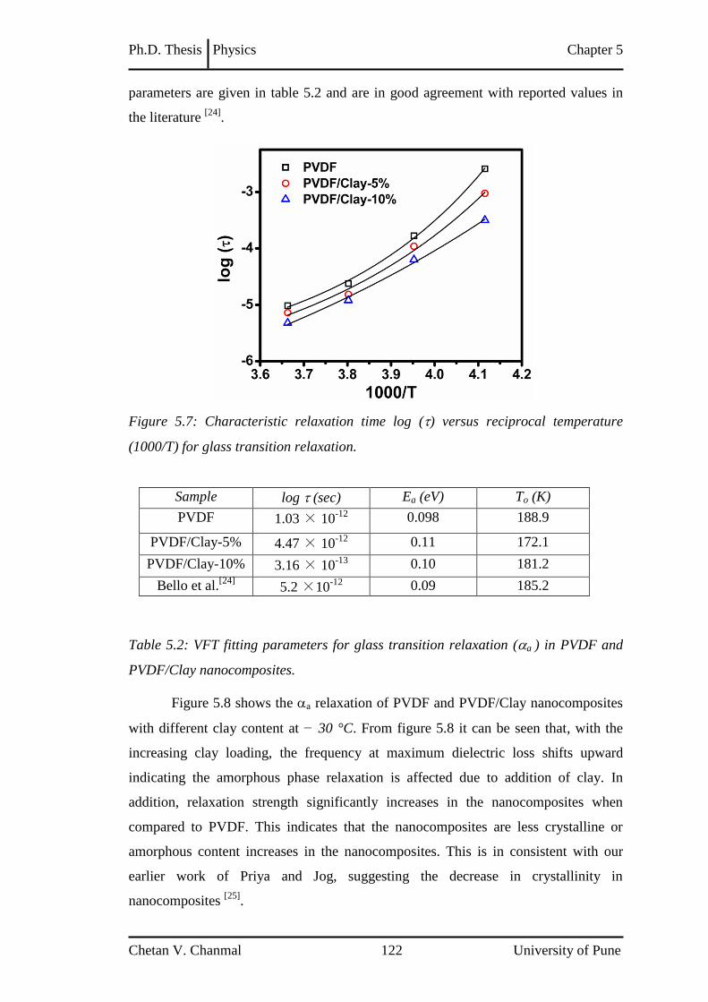
Ph.D. Thesis Physics Chapter 5
Chetan V. Chanmal 122 University of Pune
parameters are given in table 5.2 and are in good agreement with reported values in
the literature [24]
.
Figure 5.7: Characteristic relaxation time log ( ) versus reciprocal temperature
(1000/T) for glass transition relaxation.
Sample log (sec) Ea (eV) To (K)
PVDF 1.03 × 10⁻¹²
0.098 188.9
PVDF/Clay-5% 4.47 × 10⁻¹²
0.11 172.1
PVDF/Clay-10% 3.16 × 10⁻¹³
0.10 181.2
Bello et al.[24]
5.2 ×10⁻¹²
0.09 185.2
Table 5.2: VFT fitting parameters for glass transition relaxation (a ) in PVDF and
PVDF/Clay nanocomposites.
Figure 5.8 shows the a relaxation of PVDF and PVDF/Clay nanocomposites
with different clay content at − 30 °C. From figure 5.8 it can be seen that, with the
increasing clay loading, the frequency at maximum dielectric loss shifts upward
indicating the amorphous phase relaxation is affected due to addition of clay. In
addition, relaxation strength significantly increases in the nanocomposites when
compared to PVDF. This indicates that the nanocomposites are less crystalline or
amorphous content increases in the nanocomposites. This is in consistent with our
earlier work of Priya and Jog, suggesting the decrease in crystallinity in
nanocomposites [25]
.

Ph.D. Thesis Physics Chapter 5
Chetan V. Chanmal 123 University of Pune
Figure 5.8: Dielectric loss ('') versus frequency of PVDF and PVDF/Clay
nanocomposites for a relaxation at −30 °C.
AC Conductivity
Conductivity contribution to polymer has two contributions viz. dc and ac
conductivity. The measured conductivity will be = dcac. Figure 5.9(a) shows
the conductivity spectra for PVDF and PVDF/Clay nanocomposites at 30 °C.
Figure 5.9: (a) ac conductivity spectra of PVDF and PVDF/clay nanocomposites at
30°C (b) Temperature dependence of ac conductivity for PVDF/Clay-10%
nanocomposites.
The increase of conductivity with the increasing clay loading is observed. In
the low frequency region, dc conductivity dominates and conductivity increases with
increasing clay loading. At 10 wt% clay loading, dc conductivity increases upto three
(b) (a)

Ph.D. Thesis Physics Chapter 5
Chetan V. Chanmal 124 University of Pune
orders of magnitude when compared to PVDF. In case of PVDF, the dc conductivity
increases with the increasing frequency, whereas for nanocomposites the slope of
increase in conductivity becomes smaller and for 10 wt % loading almost conductivity
plateau is observed in the low frequency region. At higher frequencies, where ac
conductivity dominates, conductivity becomes frequency dependent and the slope of
increase becomes similar to PVDF.
The temperature dependence of ac conductivity is shown in figure 5.9(b). The
ac conductivity of the composites increases with increasing temperature and the
convergence of conductivity at high frequency is observed. As the frequency
decreases more and more charge carriers accumulate at the interface between the
sample surface and the electrodes, which leads to drop in ac conductivity at low
frequency. At high temperature conductivity is almost constant in the low frequency
region but after certain critical frequency is reached, conductivity increases with
increasing frequency. The transition region from dc (frequency- independent) to ac
(frequency dependent) conductivity shifts to higher frequencies with increasing
temperature.
5.I.4 Conclusions
In conclusion, we have studied the structure and dielectric properties of melt
blended PVDF/clay nanocomposites. X-ray diffraction (XRD) and FTIR studies
indicated the formation of β phase in the PVDF/clay nanocomposites. The dielectric
study of PVDF/Clay nanocomposites shows composition dependent enhancement in
permittivity. The absence of crystalline relaxation peak in dielectric loss curve for
nanocomposites also confirms the formation of β phase in PVDF/Clay
nanocomposites. The analysis of dielectric permittivity data using logarithmic model
based on effective medium theory predicted permittivity values which were lower
than the experimental values. However, the experimental values of permittivity could
be well fitted to the Vo and Shi model indicating the presence of interfacial
interaction between PVDF and clay. The complex impedance formalism analysis
further supported the presence of interfacial effects. Thus the observed increase in the
dielectric permittivity could be attributed to the presence of strong interfacial
interaction.

Ph.D. Thesis Physics Chapter 5
Chetan V. Chanmal 125 University of Pune
Section II: PVDF/Clay Nanocomposites as a Gate Dielectric in Organic FET
5.II.1 Introduction
Over the past twenty years, research in the field of organic field effect
transistors (OFET) has attracted significant research interest due to their wide range of
applications such as organic integrated circuit board, low cost radio frequency
identification tags (RFID), organic active matrix display, gas sensors, and infra red
(IR) sensor [26-28]
. OFET also offer advantage in terms of low cost, ease of process,
flexibility and light weight [29]
. Current research in this field is aimed towards design
of OFET having multifunctional applications in single device architecture.
One of the prominent applications of OFET is in the field of memory devices.
In memory devices the information is stored using physical property that displays
hysteresis in response to an applied electric field. Ferroelectric polymers such as Poly
(vinylidene fluoride) PVDF and its copolymer have been widely studied as a gate
dielectric material in OFET [30-32]
. The ferroelectricity in PVDF is found to originate
from bistable dipole polarization between hydrogen and fluorine atoms and making
the material suitable for potential memory devices. PVDF is well known polymer
which exhibits ferroelectric and pyroelectric properties. Apart from this, PVDF has
several other advantages like high Curie temperature, short switching time and good
thermal stability. Another important factor for PVDF based device is to achieve
ferroelectric phase of PVDF having polarization better than other crystalline forms
and of PVDF. In the first section of this chapter we have seen that addition of
Clay induces phase in PVDF. Although OFET based on PVDF were studied in
details in the past, OFETs based on the nanocomposites of PVDF are not studied so
far. In this section we will discuss the use of PVDF/clay nanocomposite in OFET
device. We also discuss the applications of the OFET as a non-volatile memory and
Infra red (IR) sensing device.
Also, the performance of OFET depends critically on the gate dielectric and
semiconductor interface. Dielectric constant of the gate dielectric is one of the crucial
parameter in the performance of OFET. The conventional inorganic gate dielectric
material such as SiO2 suffers from the low dielectric constant. Polymer gate dielectric
with high dielectric constant offers advantage over the inorganic gate dielectric.

Ph.D. Thesis Physics Chapter 5
Chetan V. Chanmal 126 University of Pune
Further, the non-interacting nature of organic- organic interface is also found to be
favorable in performance of OFET.
In this context we have studied use PVDF/Clay nanocomposites as a gate
dielectric material in OFET device architecture. The nanocomposite layer used in
present study offer several advantages: i) it has high dielectric constant which
increases the gate capacitance and hence charge carrier density at the semiconductor
dielectric interface, ii) it has high dielectric strength which effectively reduces the
gate leakage current, iii) it exhibits desirable ferroelectric and pyroelectric properties,
and iv) it is solution processable.
5.II.2 Experimental
In this work, bottom gate top contact of FET configuration is fabricated.
Cleaned Indium doped tin oxide (ITO) coated glass slide (Aldrich) is used as a gate
electrode. Gate dielectric was prepared by spin coating PVDF/Clay nanocomposite
solution onto ITO substrate. The PVDF nanocomposite with 5wt% clay loading was
used as a gate dielectric in OFET configuration. For this, solution of 5wt%
PVDF/Clay nanocomposite in DMF: Acetone (1:1) is prepared and spin coated at
1500 rpm for 1 min. The film is then annealed at 140 C for 2 hr to enhance the
crystallinity of the films. The film thickness was around 2 m, measured using
Dektak profilometer. An additional layer of poly (4-vinyl phenol) (PVP-crosslinker)
solution is deposited onto PVDF layer. The PVP layer helps to increase electric
breakdown strength of dielectric layer and also allows the controlled growth of
Pentacene by the reduction of the substrate roughness. The PVP cross linker solution
was prepared by taking PVP (11%) and Polymelamine co-Formaldehyde (4%) in
propylene glycol monomethyl ether. The PVP Cross linker was spin coated at
1500 rpm for 1 min. The films were annealed at 100 C for 20 min and 175 C for
1 hr. The thickness of PVP layer was around 1 m. Before carrying out the FET
measurement, a capacitor structure of gate dielectric was fabricated to study the
leakage current. In all devices leakage current was found to be less than 10-09
A.

Ph.D. Thesis Physics Chapter 5
Chetan V. Chanmal 127 University of Pune
Pentacene was used as a semiconducting channel layer in the OFET
configuration. Pentacene was deposited by thermal evaporation process (at pressure of
10-06
Torr). The thickness of the semiconductor channel layer is around 50-70 nm.
Finally, pure gold was deposited by PLD process through shadow masking to form
the top drain source contact. The thickness of the gold contacts was around 100 nm.
The transistor has dimensions of channel length 150 m and width 1500 m. The
schematic of device architecture is shown in figure 5.10 (a). The device also shows
high optical transparency as shown in figure 5.10 (b). The I-V characteristics were
performed on Agilent make semiconductor analyzer. For comparison OFET using
only PVDF as dielectric is also prepared. Ferroelectric properties of
metal/PVDF/metal capacitors with Au bottom and Al top electrodes were obtained
using Radiant Technologies PE loop analyzer.
Figure 5.10 (a) shows the schematic of device architecture (b) photographs of actual
FET device showing high optical transparency.
(a) (b)

Ph.D. Thesis Physics Chapter 5
Chetan V. Chanmal 128 University of Pune
5.II.3 Results and Discussion
5.II.3.1 Structural Analysis
The crystalline structure of spin casted PVDF/Clay nanocomposites is studied
using ATR-FTIR spectroscopy. Figure 5.11(a) compares FTIR pattern of melt process
and spin coated PVDF/Clay nanocomposite. It may be recalled that, melt
compounded PVDF/Clay nanocomposites crystallizes into phase. From the figure
5.11 (a), it can be seen that FTIR spectra corresponding to melt press film and spin
coated samples are almost similar. This indicates that spin coated PVDF/Clay thin
film also crystallizes into phase of PVDF.
MFM structure was fabricated for ferroelectric loop analysis. Polarization
hysteresis data of spin coated PVDF/Clay nanocomposites is presented in the figure
5.11 (b). The polarization curve shows typical hysteresis loop indicating the
ferroelectric nature of gate dielectric layer. The nanocomposite film shows remanent
polarization (Pr) of 1.2 C/cm2 with the coercive voltage (Vc) of 9 V. The remanent
polarization (Pr) is less than the reported value of 7 C/cm2 [29]
. It is to be noted that
these measurements were carried out on the as deposited films of PVDF/Clay
nanocomposites and the films were not poled.
Figure 5.11: (a) ATR-FTIR spectra of spin coated and melt compounded PVDF/clay
nanocomposite and (b) polarization hysteresis (P-E curve) of metal-insulator-metal
(MIM) capacitor structure of PVDF/clay nanocomposite.
(a)
(b)

Ph.D. Thesis Physics Chapter 5
Chetan V. Chanmal 129 University of Pune
5.II.3.2 Transistor Characteristics of PVDF/Clay OFET
The output characteristic of PVDF/clay nanocomposite FET is shown in the
figure 5.12 (a). The FET exhibits good linear and saturation behavior. The device
operates in accumulation enhancement mode and shows p-type characteristics. Figure
5.12 (b) shows the typical transfer curve for bottom gated PVDF/Clay nanocomposite
FET. In the transfer curve, the gate bias (VGS) was swept from + 90 V to – 90 V and
back with the constant drain voltage (VDS) of – 30 V. A sharp increase in the drain
current (IDS) with negative gate bias was observed due to the holes accumulating at
the semiconductor dielectric interface. When the gate voltage is returned to zero, IDS
almost retained its value indicating polarization of dipoles in PVDF. The drain current
has bistability at zero gate bias due to ferroelectric polarization of gate dielectric
material. The transfer curve shows the hysteresis loop in the clockwise direction.
Hysteresis in the OFET is normally related to the bistability in the operational
transistor current and its origin can be attributed to different mechanisms. Typically,
charge trapping process at the semiconductor dielectric interface induces
anticlockwise hysteresis in the p channel FET. Whereas, the presence of dipolar
groups in the dielectric causes the clockwise hysteresis in the p-channel FET
attributing to the ferroelectric nature of the gate dielectric layer. Thus the observed
hysteresis in the present study is due to ferroelectric polarization of the gate dielectric
material rather than the charge trapping mechanism.
For comparison, we also fabricated the Pentacene FET with pristine PVDF as
a gate dielectric. Figure 5.12(c) & (d) shows output and transfer characteristics of
PVDF based device. The output and transfer characteristics show that device exhibit
p-type characteristics operating in accumulation mode. On comparing the transfer
characteristics with the PVDF/clay FET, it clearly shows that hysteresis loop is not
prominent in PVDF based FET device. This is expected as the spin casting of PVDF
film forms predominately non-polar phase and therefore significant hysteresis is not
observed in the transfer characteristics.
The field effect mobility (FE was calculated from the slope of the square root
of the drain current versus gate voltage in the saturation regime using following
equation.
IDS= (W/2L) FE C (VG - Vth) 2

Ph.D. Thesis Physics Chapter 5
Chetan V. Chanmal 130 University of Pune
Where, IDS is drain source current, FE is the field effect mobility, Vth is
threshold voltage and C is the capacitance of the gate dielectric. Table 5.3 shows the
device parameters of FET device. From table 5.3, it is clear that both the mobility and
on/off ratio has been improved in the case PVDF/Clay nanocomposite OFET
compared PVDF OFET.
Table 5.3: Device parameters of PVDF and PVDF/Clay FET.
Figure 5.12: (a) Output and (b) transfer characteristics of PVDF/Clay
nanocomposite FET, (c) Output and (d) transfer characteristics of PVDF FET.
Dielectric layer Mobility (cm2V
-1s
-1) On/Off Ratio Threshold Voltage
PVDF FET 0.004 6.69 × 10 +01
25
PVDF/Clay FET 0.030 1.39 × 10 +03
– 5

Ph.D. Thesis Physics Chapter 5
Chetan V. Chanmal 131 University of Pune
5.II.3.3 Nonvolatile Memory OFET
In memory OFET, transistor can be established into ON or OFF state by
means of voltage applied to gate electrode. Memory retention of our device is studied
by applying writing voltage to the gate with respect to short circuited drain source
electrodes. Memory retention properties of PVDF/Clay nanocomposite device is
studied by measuring IDS in the ON and OFF state under zero gate bias with a
constant VDS of – 50 V. In the memory retention studies, for OFF state measurement a
gate voltage pulse of + 90 V is applied for 10 s to drive the device into OFF state and
the drain source (IDS) current is measurement as a function of time. Similarly, for ON
state measurement a gate voltage pulse of – 90 V was applied for 10 seconds to make
the device into ON state and drain source current (IDS) is measurement as a function
of time. Figure 5.13 shows the results of memory retention measurement. Drain
source current (IDS) current does not show any significant drop in ON current over a
long time period inspite of small decrease in the ON current at the beginning whereas
OFF current seems to be even more stable. An asymptotic nature of ON and OFF
behavior is also similar to earlier work presented in the literature [28, 31]
.
Figure 5.13: Both ON and OFF state currents were measured at zero gate voltage
with the continuous drain voltage (VDS) of – 50 V after single gate voltage pulse of
– 90 V and +90 V for ON and OFF current, respectively.

Ph.D. Thesis Physics Chapter 5
Chetan V. Chanmal 132 University of Pune
5.II.3.4 Infrared (IR) Response of the Device
Infrared (IR) response of the device is determined by illuminating the device
by IR lamp and monitoring drain source (IDS) current. The drain source current (IDS) is
recorded at a constant drain source voltage (VDS = – 30 V) and gate voltage
(VGS = – 30 V). The response of the device is shown in figure 5.14. Upon the
illumination of the device with IR radiation, an increase in IDS is observed and with
the removal of IR radiation, drain current was found to decrease immediately. It is
noteworthy that nanocomposite OFET device shows significant response to IR
radiations, compared to neat PVDF OFET. The increase in the drain current by IR
illumination can be understood by considering the change in effective mobility of
pentacene and due to the positive pyroelectric coefficient of PVDF dielectric layer.
When the device is illuminated with IR radiation, thermally activated hopping
transport in pentacene is also expected to be enhanced which effectively increases the
drain current. In addition to this, positive pyroelectric coefficient of gate dielectric
increases effective gate voltage bias which helps in the increase of drain current. The
pyroelectric nature of gate dielectric is discussed in the next section.
Figure 5.14: IR response of (a) PVDF/Clay nanocomposite OFET (b) PVDF OFET
device.
(a)
(a)
(b)
(b)
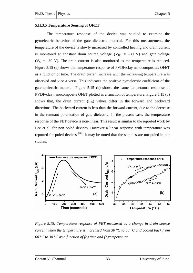
Ph.D. Thesis Physics Chapter 5
Chetan V. Chanmal 133 University of Pune
5.II.3.5 Temperature Sensing of OFET
The temperature response of the device was studied to examine the
pyroelectric behavior of the gate dielectric material. For this measurement, the
temperature of the device is slowly increased by controlled heating and drain current
is monitored at constant drain source voltage (VDS = –30 V) and gate voltage
(VG = –30 V). The drain current is also monitored as the temperature is reduced.
Figure 5.15 (a) shows the temperature response of PVDF/clay nanocomposites OFET
as a function of time. The drain current increase with the increasing temperature was
observed and vice a versa. This indicates the positive pyroelectric coefficient of the
gate dielectric material. Figure 5.15 (b) shows the same temperature response of
PVDF/clay nanocomposite OFET plotted as a function of temperature. Figure 5.15 (b)
shows that, the drain current (IDS) values differ in the forward and backward
directions. The backward current is less than the forward current, due to the decrease
in the remnant polarization of gate dielectric. In the present case, the temperature
response of the FET device is non-linear. This result is similar to the reported work by
Lee et al. for non poled devices. However a linear response with temperature was
reported for poled devices [28]
. It may be noted that the samples are not poled in our
studies.
Figure 5.15: Temperature response of FET measured as a change in drain source
current when the temperature is increased from 30 °C to 60 °C and cooled back from
60 °C to 30 °C as a function of (a) time and (b)temperature.
(a) (b)

Ph.D. Thesis Physics Chapter 5
Chetan V. Chanmal 134 University of Pune
5.II.4 Conclusions
In conclusion, the dielectric studies show the composition dependent
enhancement in permittivity of PVDF/Clay nanocomposites. The absence of
crystalline relaxation peak in permittivity loss curve for nanocomposites confirms the
formation of β phase in PVDF/Clay nanocomposites. The X-ray diffraction study of
PVDF/clay nanocomposites also confirms the formation of ferroelectric β phase
crystallization of PVDF in the nanocomposites. The analysis of dielectric permittivity
data using logarithmic model based on effective medium theory predicted permittivity
values which were lower than the experimental values. However, the experimental
values of permittivity could be well fitted to the Vo and Shi model indicating the
presence of interfacial interaction between PVDF and clay. The complex impedance
formalism analysis further supported the presence of interfacial effects. Thus the
observed increase in the dielectric permittivity could be attributed to the presence of
strong interfacial interaction.
We have also demonstrated the feasibility of using PVDF/Clay nanocomposite
as gate dielectric layer in the FET device. The device exhibit excellent transistor
performance with p-type operation. The device shows a good response to the IR
radiation. The successful operation of FET device provides a promising route for
realizing both memory storage and IR sensing applications in a single device.
5.II.5 References
1. J. Lu, K. Moon, C.P. Wong, Electronic Components and Technology
Conference,Proceedings. 57th
, 2007.
2. Y. Bai, Z.Y. Cheng, V. Bharti, H.S. Xu, Q. M. Zhang, Appl. Phys. Lett., 2000,
76, 3804.
3. A. Maliakal, H. Katz, P.M. Cotts, S. Subramoney, P. Mirau, J. Am. Chem. Soc.,
2005, 127, 14655.
4. Z.M. Dang, H.P. Xu, D. Xie, L. Li, Mater. Lett., 2000, 61, 511-515.
5. C.V. Chanmal, J.P. Jog, eXpress Polymer Letters, 2008, 2, 294.
6. D. H. Kuo, C. C. Chang, T. Y. Su, W. K. Wang, B. Y. Lin, J. Eur. Cera. Soc.,
2001 21, 1171.
7. M. Arbatti, X. Shan, Z. Cheng, Adv. Mater., 2007, 19, 1369-1372.

Ph.D. Thesis Physics Chapter 5
Chetan V. Chanmal 135 University of Pune
8. Z. M. Dang, L.Z. Fan, Y. Shen, C.W. Nan, Mater. Sci. Eng. B., 2003,103, 140.
9. B. Hilczer, J. Kulek, E. Markiewicz, M. Kosec, B. Malic, J. Non-Crystalline
Solids, 2002, 305 167.
10. Suprakas Sinha Ray, Masami Okamoto, Prog. Polym. Sci., 2003, 28, 1539–
1641.
11. R.J. Sengwa, Shobhna Choudhary, Sonu Sankhla, Composites Sci. and tech.,
2010, 70, 1621-1627.
12. Priya L, J. P. Jog, J. Polym Sci, Polym Phys., 2002, 40, 1682.
13. Lei Yu, Peggy Cebe, Journal of Polymer Science Part B: Polymer Physics,
2009, 47, 2520-2532.
14. Y. Rao, J. Qu, T. Marinis, C.P. Wong, IEEE transactions on components and
packaging technologies, 2000, 23, 680.
15. M.G. Todd, F. G. Shi, Microelectronics Journal, 2002, 33, 627-632.
16. K. Wakino, T. Okada, N. Yoshida, K. Tomono, J. Amer. Cera. Soc., 1993, 76,
2588-94.
17. Y. Wang, J. Wang, F. Wang, S. Li, J. Xiao, Polymer Bulletin, 2008, 60, 5.
18. R. Popielarz, C.K. Chiang, R. Nozaki, J. Obrzut, Macromolecules, 2001, 34,
5910-5915.
19. H.T. Vo, F. G. Shi, Microelectronics Journal, 2002, 33, 409.
20. P. Murugaraj, D. Mainwaring, N. Mora-Huertas, J. Appl. Phys., 2005, 98,
054304.
21. S. De, A. Dey, S.K. De, Eur. Phys. Journal B, 2005, 46, 355.
22. G. Liu, C. Wang, C. Wang, J. Qui, M. He, J. Xing, K. Jin, H. Lu, G. Yang, Appl.
Phys. Lett., 2008, 92, 122903.
23. H. Lu, X. Zhang, H. Zhang, J. Appl. Phys., 2006,100, 054104.
24. A. Bello, E. Laredo, M. Grimau, Physical review B, 1999, 60, 12764.
25. Priya L., J. P. Jog, J Polym Sci, Polym Phys,2002,40,1682.
26. B. Crone, A. Dodabalapur, A. Gelperin, L. Torsi, H. E. Katz, Appl. Phys. Lett.,
2001, 78, 15.
27. Tran Quang Trung, Nguyen Thanh Tien, Young Gug Seol, Nae-Eung Lee,
Organic Electronics, 2012, 13, 533-540.
28. Nguyen Thanh Tien, Young Gug Seol, Le Huynh Anh Dao, Hwa Young Noh,
Nae-Eung Lee, Adv. Mater., 2009, 21, 910–915.

Ph.D. Thesis Physics Chapter 5
Chetan V. Chanmal 136 University of Pune
29. Ronald C. G. Naber, Kamal Asadi, Paul W. M. Blom, Dago M. de Leeuw, Bert
de Boer, Adv. Mater., 2009, 21, 1-13.
30. Seok Ju Kang, Youn Jung Park, Jinwoo Sung, Pil Sung Jo, Cheolmin Park, Kap
Jin Kim, Beong Ok Cho, Appl. Phys. Lett., 2008, 92, 012921.
31. Sun Kak Hwang, Sung‐Yong Min, Insung Bae, Suk Man Cho, Kang Lib
Kim,Tae‐Woo Lee, Cheolmin Park, Organic Electronics, 2012, 13, 491–497.
32. K. N. Narayanan Unni, Remi de Bettignies, Sylvie Dabos-Seignon, Jean-Michel
Nunzi Appl. Phys. Lett., 2004, 85, 10.

Chetan V. Chanmal 137 University of Pune
Chapter 6
Conclusions and Future Scope
This chapter describes the salient features of the results presented in this thesis and the
scope for future work.

Ph.D. Thesis Physics Chapter 6
Chetan V. Chanmal 138 University of Pune
6.1 Summary of the Thesis
The main objective of the thesis was to fabricate nanocomposites based on
PVDF using three different types of nanofillers viz. BaTiO3, MWCNT and Clay. The
nanocomposites were fabricated using melt compounding technique, pulsed laser
deposition, and electrospinning technique. The effect of nanofillers on the dielectric
properties were studied in detail and the applications of nanocomposites in low
thermal emissivity and organic field effect device (OFET) were explored.
The major results of the work carried in the thesis can be summarized as following
1. PVDF/BaTiO3 bulk nanocomposites were prepared by melt mixing technique. The
frequency and temperature dependence of dielectric properties were studied in
detail. Permittivity of PVDF increased with increasing loading of BaTiO3. The
nanofibers of PVDF/BaTiO3 nanocomposites were prepared by electrospinning
technique. The thermal emissivity of electrospun nanofibers were measured using
a prototype instrument based on thermopile. The measurement showed that
electrospun nanofibers showed lower thermal emissivity compared to the melt
pressed PVDF/BaTiO3 nanocomposites. The reduction in the thermal emissivity
was attributed to the porous and non-woven morphology of the electrospun fibers.
The low thermal emissivity of electrospun fibers makes it a suitable material for
camouflaging in defense related applications.
2. PVDF/MWCNT nanocomposites thin films were prepared by pulsed laser
deposition (PLD). The addition of MWCNT showed enhancement in the
ferroelectric phase of PVDF. The dielectric studies showed significant
enhancement in the permittivity when MWCNT loading was near to percolation
threshold. The percolation threshold was found to be higher than for the bulk
sample due to reduction in aspect ratio of MWCNT during PLD process. This
increase in percolation threshold allowed higher loading of MWCNT (upto 7
wt%) into polymer matrix. Figure 6.1 compares the dielectric permittivity of
PVDF/MWCNT nanocomposites with PVDF/BaTiO3 and PVDF/clay
nanocomposites. It can be seen that, significant increase in the permittivity is
observed in PVDF/MWCNT nanocomposites at relatively lower filler loading.
Comparatively, very small increase is observed in the PVDF/BaTiO3

Ph.D. Thesis Physics Chapter 6
Chetan V. Chanmal 139 University of Pune
nanocomposites. Thus, percolative composites system is found to be superior
compared to the polymer/ceramic nanocomposites.
Figure 6.1: Comparison of dielectric permittivity of PVDF/MWCNT with different
loading of MWCNT at 10+02
Hz frequency. For comparison, data for
PVDF/BaTiO3 and PVDF/Clay nanocomposites were also shown.
The conductivity of PVDF/MWCNT nanocomposites also found increase with
the MWCNT loading. The PVDF/MWCNT nanocomposite layer was studied as
an active channel layer in OFET configuration. The device showed strong field
modulation of drain current when MWCNT loading was near to percolation
threshold (5 wt %). Thus the nanocomposite route offers a unique way of realizing
organic transistor.
3. PVDF/Clay nanocomposites were prepared by melt blending technique. Dielectric
studies showed enhancement in the dielectric permittivity in nanocomposites
which was attributed to the interfacial interactions between filler and polymer
matrix. The dielectric permittivity increased to 165 with 10 wt% loading of clay.
The fitting experimental data was fitted to Vo-Shi model which confirm the
interface contribution to dielectric permittivity.

Ph.D. Thesis Physics Chapter 6
Chetan V. Chanmal 140 University of Pune
The organic field effect transistor (OFET) was fabricated using thin films of spin
coated PVDF/Clay nanocomposites as a gate dielectric material. The device
showed excellent transistor characteristics with p-type operation. Due to the
ferroelectric property of PVDF/Clay nanocomposites, OFET device showed
excellent memory retention characteristics. Moreover, the device also showed
response to IR signal due to the pyroelectric property by PVDF. Thus, the direct
integration of PVDF/clay nanocomposites as gate dielectric layer demonstrated
the efficiency of device for IR sensing and non-volatile memory applications.
6.2 Scope for Future Work
1. All Organic FET
With electrospinning technique it is possible to fabricate indium tin oxide (ITO)
nanofibers on a given substrate. The electrospun ITO nanofibers show good
conductivity level making an alternative candidate for gate electrode material in
OFET. It will be interesting to study the fabrication of OFET with electrospun ITO
nanofibers as gate electrodes. In our studies, we have independently used
PVDF/MWCNT nanocomposites as channel layer and PVDF/Clay nanocomposites as
ferroelectric gate dielectric layer. The integration of all these components into single
device can bring unique approach of fabricating OFET with multifunctional
properties. Moreover, flexible substrate can be also used for device fabrication. This
flexible all organic FET can have potential applications in electronic devices like
handheld portable sensors or detectors.
2. Electromagnetic Interference (EMI) Shielding Material
In recent years, electronics field in the area of wireless communication
systems, high speed devices, cellular phones etc. has gained rapid development. Due
to the increasing use of high frequency and high bandwidth in this technology, there
are chances of deterioration in the incoming radio signals which is known as
Electromagnetic interference (EMI). This interference has an adverse effect on the
communication systems. Hence there is need of material which acts as a microwave
absorber. Typically, metals and metallic composites are used as a shielding material
due to their good electrical conductivity. However, these metals suffer from corrosion,
poor chemical resistance, difficult processing and high density. Hence, polymer based

Ph.D. Thesis Physics Chapter 6
Chetan V. Chanmal 141 University of Pune
composites were increasingly investigated as an alternative for EMI shielding material
[1-3]. In this context, PVDF/MWCNT nanocomposites can offer potential application
in EMI shielding applications.
3. Multiferroic Nanocomposites
Multiferroic materials are the one which simultaneously exhibit ferroelectricity
and ferromagnetism. Recently, multiferroic materials stimulated an increasing
attention as prospective candidate for potential applications in emerging fields like
spintronics and sensor devices. The key performance of a multiferroic material relies
on strong magnetoelectric coupling which control magnetization via polarization
and vice versa. Typically, magnetoelectric coupling refers to the magnetic induction
by an electric field or electrical polarization by a magnetic field. However, natural
single phase multiferroic materials are rare or their performance is rather very weak at
room temperature. This difficulty can be solved by fabricating composite material or
hybrid materials having diverse properties [4, 5]
.
Polymer based multiferroic materials has inherent advantage of ease of processing,
mechanical flexibility, and light weight. PVDF can offer unique advantage as polymer
based multiferroic as it is known for its ferroelectric, piezoelectric and pyroelectric
properties. The composite of PVDF with magnetoelectric materials like Fe3O4,
CoFe2O4, and ferrites can be interesting system for multiferroic materials applications.
6.3 References
1. Young-In Lee, Kun-Jae Lee, Ki Do Kim, Hee Taik Kim, Young-Wook Chang,
Shin-Choon Kang, and Yong-Ho Choa, J. Nanosci. Nanotechnol., 2007, 7, 11.
2. Feng-Yu Yang, Kuo-Jui Chang, Meei-Yu Hsu, Cheng-Chin Liu, J. Mater. Chem.,
2008, 18, 5927–593.
3. Chun-Sheng Zhang, Qing-Qing Ni, Shao-Yun Fu , Ken Kurashiki, Composites
Science and Technology , 2007, 67, 2973–2980.
4. Ce-Wen Nan, M. I. Bichurin, Shuxiang Dong, D. Viehland, G. Srinivasan, J.
Appl. Phys., 2008, 103, 031101.
5. O. D. Jayakumar, B. P. Mandal, J. Majeed, G. Lawes, R. Naik, A. K. Tyagi, J.
Mater. Chem. C, 2013, 1, 3710–3715.

Chetan V. Chanmal 142 University of Pune
Appendix-I
Magneto-Dielectric Properties of
PVDF/Fe3O4 Nanocomposites
The magneto dielectric properties of PVDF/Fe3O4 nanocomposites fabricated by melt
processing are presented here. The dielectric relaxation spectroscopy (DRS) technique
is used to investigate the dielectric relaxation and molecular mobility in PVDF/Fe3O4
nanocomposites. Dielectric spectroscopy showed an increase in the permittivity of
nanocomposites in the whole frequency range studied. The magnetic properties show
a ferromagnetic behavior in polymer nanocomposites. The fabricated nanocomposites
have potential for use in electronics packaging substrate as an alternative substrate
owing to their good thermal, mechanical and dielectric properties.

Ph.D. Thesis Physics Appendix-I
Chetan V. Chanmal 143 University of Pune
A.1 Introduction
Magnetic particles embedded in ferroelectric polymer matrix can have
excellent potential application such as magneto-optical storage devices, flexible
electronic devices etc. Hybrid inorganic–organic nanocomposite materials are of
current interest because of their multifunctionality, ease of processability, and
potential for large-scale manufacturing. Many attractive properties of polymers like
non-corrosiveness, light weight, mechanical strength, and dielectric tunability can be
utilized along with magnetic
and optical properties of nanoparticles to make
multifunctional materials [1-3]
. The advantages of these materials in electromagnetic
interference (EMI) reduction are due to desirable properties like frequency agility,
light weight, and non-corrosive nature.
Inclusion of ferromagnetic nanoparticles in polymers is especially important as
magnetic nanoparticles have shown promise in various potential applications like
spin-polarized devices, carriers for drug delivery, magnetic recording media, high-
frequency applications,
etc.[4,5]
However, for most of these highly specialized
applications, there is a practical need to disperse the nanoparticles in non-magnetic
media that can be easily processed. Polymer materials are very well suited for this
purpose. Magnetic
nanoparticles embedded in polymer matrices have excellent
potential for electromagnetic device applications like electromagnetic interference
suppression.
Advances made to prepare the multifunctional nanocomposites have led great
improvement in this field. Several approaches have been developed to synthesize
these composites in bulk as well as thin-film forms like sol gel, vacuum evaporation
from powders, layer-by-layer self assembly, etc. In the present work, we have
synthesized polymer nanocomposites of Poly (vinylidene fluoride) doped with varying
concentrations of Fe3O4 nanoparticles (~30-50 nm in size). These nanocomposites
were processed using simple melt blending technique. The polymer processing
conditions were optimized to achieve good uniform dispersion of the nanoparticles in
the polymer matrix.

Ph.D. Thesis Physics Appendix-I
Chetan V. Chanmal 144 University of Pune
A.2 Experimental
Materials
PVDF Grade, Solef 1008 procured by Solvay Belgium is used for this study.
Fe3O4 nanoparticles were procured from Aldrich Chemicals. The Fe3O4 were used as
received for the experiments without any chemical treatment for surface modification.
Figure A.1 shows the TEM and XRD of Fe3O4 nanoparticles. TEM micrograph shows
the spherical particle shape of Fe3O4 nanoparticles. The particle size of Fe3O4 was
estimated to be 30–50 nm. The XRD of the nanopowder exhibits the characteristic
peaks of Fe3O4. The peaks at 30.2°, 35.4°, 43.3°, 53°, 57.2° and 62.9° corresponding
to the (220), (311), (400), (422), (511) and (440) planes of Fe3O4 confirming the cubic
spinel structure [6]
.
Figure A.1: (a) TEM micrograph and (b) X-ray diffraction pattern of Fe3O4
nanoparticles.
Fabrication of PVDF /Fe3O4 nanocomposites:
The nanocomposites of PVDF with various weight percent of Fe3O4 (10, 20,
30, 40 % wt/wt) were prepared by melt mixing in Thermo Haake Polylab batch mixer
at 200 C, with 60 rpm and residence time of 5 minutes. Prior to melt processing, all
the materials were dried in an air circulatory oven at 70 C for 24 hr. The films of
uniform thickness were compression molded at 200 C under 5-ton pressure using
Carver Press (Germany). The thickness of the films was around 0.4 to 0.5 mm.
(a) (b)

Ph.D. Thesis Physics Appendix-I
Chetan V. Chanmal 145 University of Pune
A.3 Results & Discussion
A.3.1 Dielectric Studies
The frequency dependence of the dielectric properties of PVDF/Fe3O4
nanocomposites with various volume fraction of the Fe3O4 is shown in Figure A.2 (a)
and (b). It can be seen that the dielectric permittivity depends on both frequency and
filler loading. The dielectric permittivity for neat PVDF is around 7 and it increases to
38 for 40 wt% of Fe3O4 nanoparticles loading. With increasing frequency dielectric
permittivity decreases in PVDF and similar trend is followed in nanocomposites. It is
worth to note that the dielectric permittivity is increased in the whole frequency range
of measurement. The increment in the permittivity in the high frequency region brings
the interest of these materials for application in high frequency electronic devices.
The high values of permittivity observed in the nanocomposites may be due to the
interfacial effects in polymer nanocomposites. For PVDF and nanocomposites up to
30% filler loading, dielectric constant is less dependent on frequency and whereas for
40% loading a strong frequency dependence is seen in the dielectric spectra.
Figure A.2: Frequency dependence of (a) dielectric permittivity (’) (b) loss (tan ) of
PVDF and PVDF/Fe3O4 nanocomposites.
In dielectric permittivity spectra, strong frequency dispersion regions are
observed above frequency 10+06
Hz and a frequency independent region in between.
Hence the dispersion observed in the permittivity originates from the dielectric
relaxation processes in polymer nanocomposites. The dielectric dispersion located at
2 × 10+07
Hz is attributed to glass transition relaxation.
(a) (b)
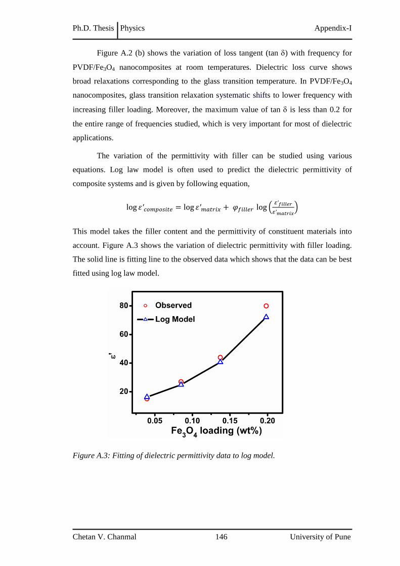
Ph.D. Thesis Physics Appendix-I
Chetan V. Chanmal 146 University of Pune
Figure A.2 (b) shows the variation of loss tangent (tan ) with frequency for
PVDF/Fe3O4 nanocomposites at room temperatures. Dielectric loss curve shows
broad relaxations corresponding to the glass transition temperature. In PVDF/Fe3O4
nanocomposites, glass transition relaxation systematic shifts to lower frequency with
increasing filler loading. Moreover, the maximum value of tan is less than 0.2 for
the entire range of frequencies studied, which is very important for most of dielectric
applications.
The variation of the permittivity with filler can be studied using various
equations. Log law model is often used to predict the dielectric permittivity of
composite systems and is given by following equation,
This model takes the filler content and the permittivity of constituent materials into
account. Figure A.3 shows the variation of dielectric permittivity with filler loading.
The solid line is fitting line to the observed data which shows that the data can be best
fitted using log law model.
Figure A.3: Fitting of dielectric permittivity data to log model.

Ph.D. Thesis Physics Appendix-I
Chetan V. Chanmal 147 University of Pune
A.3.2. Magnetic Properties
Figure A.4 shows the field dependent magnetic properties of PVDF/Fe3O4
nanocomposites at 300 °K. The hysteresis loop provides the important information
relating to the magnetic properties of the materials viz. saturation magnetization,
remnant magnetization and coercivity. M-H hysteresis loop measurements done at
300 °K with the magnetic field swept back and forth between 10 kOe and -10 kOe is
shown in figure A.4. The magnetic behavior of PVDF/Fe3O4 nanocomposites with
different content of Fe3O4 nanoparticles shows a clear magnetic hysteresis loops at
300 °K. The observance of hysteresis loop tells that the blocking temperature (TB) of
the sample was higher than the room temperature. The magnetic measurement shows
that nanocomposites exhibit ferromagnetic nature of nanoparticles. The variation of
the ferromagnetic response was consistent with the varying volume concentration of
the nanoparticles. It is observed that the saturation magnetization increases linearly
with increasing filler loading which is consistent with the mean field dependence of
the magnetization of iron oxide nanoparticles. It can be seen that the coercive field
(Hc) at 300 °K for different concentrations of Fe3O4 in PVDF remains roughly the
same as 76 Oe. The saturation magnetization in polymer loaded nanoparticles system
is generally expected to be lower than that of the bulk materials.
Figure A.4: (a) M-H curves at 300 °K for Fe3O4 and PVDF/Fe3O4 nanocomposites
(arrows indicates towards corresponding Y-axis) (b) Same graph with magnified
image.
(a)
(b)

Ph.D. Thesis Physics Appendix-I
Chetan V. Chanmal 148 University of Pune
The magnetic properties can be influenced by the size, structure, and morphologies of
the materials. The magnetic parameters extracted from the measurements are
summarized in Table I.1. Remnant magnetization also increases with increasing filler
content. However this increase observed is non-linear. Unlike saturation
magnetization, remenance magnetization is influenced by particle-particle interaction
which is governed by the particle concentration inside the polymer matrix.
Table I.1: Magnetic measurement results of PVDF/Fe3O4 nanocomposites.
A.4 Conclusions
In conclusion, we have studied the dielectric and magnetic properties of melt
compounded PVDF/Fe3O4 nanocomposites. The nanocomposite shows composition
dependent dielectric permittivity and magnetic properties. The dielectric permittivity
was found to increase with increasing loading of Fe3O4 nanoparticles. The variation of
dielectric permittivity with filler loading can be fitted very well using log law model.
The magnetic measurement studies show that nanocomposites exhibit ferromagnetic
nature of nanoparticles. Thus, the nanocomposites material can be suitable material
for electromagnetic shielding (EMI) material application.
Composition Ms
(emu/gm)
Coercive field
(Hc) (Oe)
Remnant
magnetization(MR)
(emu/gm)
Fe3O4 50.3 74 5.3
PVDF/Fe3O4-10% 4.7 76 0.42
PVDF/Fe3O4-20% 9.5 76 1.06
PVDF/Fe3O4-30% 14.6 76 1.65
PVDF/Fe3O4-40% 18.9 76 1.75

Ph.D. Thesis Physics Appendix-I
Chetan V. Chanmal 149 University of Pune
A.5 References
1. Jeffrey Pyun, Polymer Reviews, 2007, 47, 231–263.
2. Natalia Frickel, Anna Gutina Greenbaum, Moshe Gottlieb, Annette M. Schmidt, J.
Phys. Chem. C. 2011, 115, 10946–10954.
3. K. Devi Chandrasekhar, A. K. Das, A. Venimadhav, Applied Physics Letters,
2011, 98, 122908.
4. Masoumeh Bayat, Heejae Yang, Frank Ko, Polymer, 2011, 52, 1645-1653.
5. P. Martins, C.M. Costa, S. Lanceros-Mendez, Appl. Phys. A., 2011, 103, 233–237.
6. G. H. Qiu, Q. Wang, M. Nie, Macromol. Mater. Eng. 2006, 291, 68.

Chetan V. Chanmal 150 University of Pune
List of Publications
1. “Enhanced dielectric permittivity in poly (vinylidene) fluoride/multiwalled
carbon nanotubes nanocomposite thin films fabricated by pulsed laser
deposition”, Chetan Chanmal, Meenal Deo, Jyoti Jog, Applied Surface
Science, 2011, 258, 1256– 1260.
2. “Strong electric field modulation of transport in PVDF/MWCNT
nanocomposite near the percolation threshold”, Chetan Chanmal, Meenal
Deo, Abhimanyu Rana, Jyoti Jog, Satishchandra Ogale, Solid State
Communications, 2011, 151, 1612-1615.
3. “Catalyst free novel synthesis of single layer graphene (SLG) and its
application in high current O-FET and phototransistor based on P3HT / SLG
composite”, Prasad Yadav, Chetan Chanmal, Aniruddha Basu, Lily Mandal,
Jyoti Jog, Satishchandra Ogale, RSC Advances,2013,3,18049-18054.
4. “Study of dielectric behavior in PVDF/Clay nanocomposites”, Chetan
Chanmal, Jyoti Jog, e-Polymers, 2009, no. 112.
5. “Electrospun PVDF/BaTiO3 nanocomposites: polymorphism and thermal
emissivity studies”, Chetan Chanmal, Jyoti Jog, Int J Plast .Technol, 2011,
15, 1-9.
6. “Dielectric relaxations in PVDF/BaTiO3 nanocomposites”, Chetan Chanmal,
Jyoti Jog, eXPRESS Polymer Letters, 2008, 2, 294-301.
7. “Magnetic and dielectric properties of polymer-ceramic composites
synthesized using a melt compound technique”, Rajshree Jotania, Chetan
Chanmal, Jyoti Jog, International Journal of Modern Physics: Conference
Series,2013, 22, 552–557.
Invited Book Chapter
1. Chapter title: “Dielectric Relaxation Spectroscopy for Polymer
Nanocomposites”, Chetan Chanmal, Jyoti Jog.
Book Title: “Characterization Techniques for Polymer Nanocomposites”
Publisher- WILEY-VCH. Chapter 7, Page 167-185, 2012.