high energy electron fluxes in dc-augmented capacitively coupled
TRANSCRIPT
High energy electron fluxes in dc-augmented capacitively coupled plasmasI. Fundamental characteristics
Mingmei Wang1,a� and Mark J. Kushner2,b�
1Department of Chemical and Biological Engineering, Iowa State University, Ames, Iowa 50010, USA2Department of Electrical Engineering and Computer Science, University of Michigan, 1301 Beal Ave., AnnArbor, Michigan 48109, USA
�Received 14 September 2009; accepted 7 December 2009; published online 29 January 2010�
Power deposition from electrons in capacitively coupled plasmas �CCPs� has components fromstochastic heating, Joule heating, and from the acceleration of secondary electrons through sheathsproduced by ion, electron, or photon bombardment of electrodes. The sheath accelerated electronscan produce high energy beams which, in addition to producing excitation and ionization in the gascan penetrate through the plasma and be incident on the opposite electrode. In the use of CCPs formicroelectronics fabrication, there may be an advantage to having these high energy electronsinteract with the wafer. To control the energy and increase the flux of the high energy electrons, adc bias can be externally imposed on the electrode opposite the wafer, thereby producing adc-augmented CCP �dc-CCP�. In this paper, the characteristics of dc-CCPs will be discussed usingresults from a computational study. We found that for a given rf bias power, beams of high energyelectrons having a narrow angular spread ��1°� can be produced incident on the wafer. Themaximum energy in the high energy electron flux scales as �max=−Vdc+Vrf+Vrf0, for a voltage onthe dc electrode of Vdc, rf voltage of Vrf, and dc bias on the rf electrode of Vrf0. The dc current fromthe biased electrode must return to ground through surfaces other than the rf electrode and so seeksout a ground plane, typically the side walls. If the side wall is coated with a poorly conductingpolymer, the surface will charge to drive the dc current through. © 2010 American Institute ofPhysics. �doi:10.1063/1.3290870�
I. INTRODUCTION
The successful use of radio frequency �rf� capacitivelycoupled plasmas �CCPs� in microelectronics fabrication ispredicated on being able to control the energy and angulardistributions of reactant species to the wafer.1 In conven-tional, single frequency CCPs, there is a tradeoff betweencontrolling the ion energy and angular distribution �IEAD�and the rate of plasma production as a function of excitationfrequency and gas pressure.2 More advanced two-frequencyCCPs separate these functions by attempting to control theIEAD using low frequency �LF� excitation ��tens ofmegahertz� and using a high frequency �HF� excitation��tens of megahertz� to control the production of theplasma and so the magnitude of fluxes to the substrate.3
New designs of CCPs are intended to provide additionalcontrol of the reactant fluxes to the substrate. One such ex-ample is a dc-augmented CCP �dc-CCP�.4–7 In this design,the electrode opposite the wafer is biased with a dc voltage�Vdc� with the intent of producing a high energy electron�HEE� beam onto the wafer having a narrow angular distri-bution. The HEE is thought to have beneficial effects in con-trolling the profile of high aspect ratio features during plasmaetching. Since the dc biases for dc-CCPs operating at tens ofmillitorr are typically many hundreds of volts, ion accelera-tion into the dc electrode, typically made of Si, can also
sputter Si atoms into the plasma. As such, the dc-CCP canalso provide some additional control over reaction chemistry.
Etching of high aspect ratio features for microelectronicsfabrication is challenged to obtain reproducible features withstraight walls and definable shapes. For example, holes withdiameters of tens of nanometers with high aspect ratios�HARs� in excess of 70 are being fabricated in large arraysfor memory cells.8 One of the challenging aspects of theseprocesses is the errant and nearly random occurrence of fea-tures that twist.8–10 That is, instead of etching vertically, thefeature will turn to the side, often after a significant fractionof the feature has already been etched. The direction of twist-ing, its frequency of occurrence, and its proximity to othertwisting features typically has no discernable pattern.
One possible explanation for twisting is errant chargingand dc-CCPs have been proposed as a remedy.5,7 As the fea-ture size shrinks to have an opening area of only hundreds ofnm2 the rate of entry of radicals and ions into the featurebegins to become statistical. For example, the time betweenthe arrivals of two ions into a feature 50 nm in diameter fora flux of 1016 cm−2 s−1 is 5 �s. This small rate of particlearrival leads to feature-to-feature statistical variations in theneutral and charged fluxes entering a single feature. Ionsarriving onto the wafer after acceleration through the sheathhave a narrower angular distribution than do thermal elec-trons. The end result is that ions penetrate deeper into fea-tures, producing random charging and electric fields that maydeflect subsequent ions and produce twisting. The HEE flux
a�Electronic mail: [email protected]�Author to whom correspondence should be addressed. Electronic mail:
JOURNAL OF APPLIED PHYSICS 107, 023308 �2010�
0021-8979/2010/107�2�/023308/10/$30.00 © 2010 American Institute of Physics107, 023308-1
Author complimentary copy. Redistribution subject to AIP license or copyright, see http://jap.aip.org/jap/copyright.jsp
with its narrow angular distribution may be able to penetrateinto HAR features and possibly neutralize this errant positivecharge.
Both experiments and simulations have been conductedto investigate the characteristics of HEEs in dc-CCPs. Kawa-mura et al.4 analytically analyzed dc-CCPs, and found that adc/rf sheath develops on the negatively biased electrode,while an rf sheath develops on the opposite electrode. Thevoltage drop in the rf sheath is nearly independent of the dcvoltage if the rf power is held constant. Recently, they alsoconducted detailed analysis of secondary electron trappingand investigated the energy distributions of secondary elec-tron fluxes incident onto the substrate.5 Particle-in-cell simu-lations of dc-CCPs were performed having a dc and a 4 MHzbias on the top electrode, while the bottom electrode wasgrounded. Their simulations showed good agreement withthe analytic solutions. They found that adding Vdc to the rfelectrode increases the mean secondary electron energy,which results in a higher discharge efficiency. Adding Vdc
altered the fraction of the rf cycle during which secondaryelectrons emitted from electrodes were trapped so that moresecondary electrons impinge on the wafer with higher en-ergy.
Denpoh et al.6 examined the role of HEEs in a dc-CCPusing a one-dimensional test particle Monte Carlo simula-tion. In their work, a dc bias was applied on the top electrodeand an rf bias at 2 MHz was applied on the bottom electrode.They found that when the rf source was off and dc sourcewas on, HEEs reached the wafer but they did not have alarge influence on discharge efficiency due to their lack ofconfinement. When both the rf source and dc source were on,the HEEs were thermalized due to the confinement from atime averaged potential well produced by the rf bias.
The properties of HEEs were also measured experimen-tally by Xu et al.7 using a single frequency dc-CCP with a dcbias applied on the top electrode and a rf bias at 13.56 MHzapplied to the bottom electrode. They proposed that the rfcycle was divided to two regimes: a dumping regime and atrapping regime. The trapping regime is when the rf sheathpotential is highly negative. HEEs are thermalized and re-turned to the bulk plasma, which contributes to a higher dis-charge efficiency. In the dumping regime, the rf sheath po-tential is positive. HEEs are accelerated by the rf sheath andpenetrate it to reach the substrate. These highly energetic anddirectional electrons were anticipated to neutralize positivecharges deep in features. At Vdc=−800 V, the HEE currentwas comparable to the ion current.
In this paper, the properties of HEE beams produced indc-CCPs sustained in Ar will be discussed with results froma two-dimensional computational investigation. In our com-panion paper these properties will be used to investigate themeans to remedy twisting during HAR etching in SiO2 indc-CCPs sustained in Ar /C4F8 /O2 gas mixtures.11 We foundthat for a given rf bias power, beams of HEEs having narrowangular spread ��1°� can be produced incident on the waferresulting from secondary electron emission from the dc bi-ased electrode. The maximum energy in the HEE flux scales�max=−Vdc+Vrf+Vrf0 for a voltage on the dc electrode of Vdc,rf voltage on the lower electrode of Vrf, and dc bias on the rf
electrode of Vrf0. Depending on the phase and amplitude ofthe rf voltage, secondary electrons from the dc electrode maybe trapped in the plasma. Similarly, HEEs resulting fromsecondary electrons emitted from the rf biased electrode canreflect from the dc electrode and be incident onto the wafer.The dc current from the biased electrode must return toground through surfaces other than the capacitively coupledrf electrode and so seeks out a ground plane. For our geom-etry, the ground plane is the side walls of the reactor. If apoorly conducting polymer is deposited on the side wall, thepolymer surface will charge to drive the required dc currentthrough the polymer layer.
The model used in this investigation is described in Sec.II followed by our discussion of properties of dc-CCPs sus-tained in argon in Sec. III. Our concluding remarks are inSec. IV.
II. DESCRIPTION OF THE MODEL
The two-dimensional hybrid plasma equipment model�HPEM� was used in this investigation. The HPEM has beenpreviously discussed in detail,12 and so is only briefly de-scribed here. The HPEM is a two-dimensional model whichconsists of separate modules which address different physi-cal phenomena. Each module consists of a time integrationover many rf cycles, during which plasma quantities �e.g.,densities and temperatures� are either recorded as a functionof position and phase or recorded only as position dependentquantities averaged over the rf cycle. These values are thenpassed to the next module and the process iterated to a cycle-average steady state. The modules used in this study are the�1� Electron Monte Carlo Simulation �EMCS� for sheath ac-celerated secondary electrons, �2� the Fluid Kinetics Module�FKM� to obtain densities, fluxes, and energies of all chargedand neutral species, as well as the electric potential from thesolution of Poisson’s equation, and �3� the Plasma ChemistryMonte Carlo Module to obtain the energy and angular distri-butions of neutrals and charged species striking the wafer.
In the FKM, continuity, momentum, and energy equa-tions are separately solved for all nonelectron species �neu-trals and ions�. Coupling between these fluids is through col-lisional exchange for momentum and energy. For bulkelectrons, only continuity and energy equations are solvedwhere fluxes are provided by the Sharfetter–Gummel formu-lation. Transport coefficients are provided as a function ofelectron temperature by solving Boltzmann’s equation. Thesevalues are updated every iteration using heavy particle molefractions, including excited states, averaged over the reactorweighted by the local electron density.
Acceleration techniques are used to speed the rate con-vergence of computed quantities. During execution of theFKM, the cycle averaged time rate of change in densities isrecorded over a period of many rf cycles. The integration isthen paused and the densities of species are increased �ordecreased� proportional to these average rates and the inte-gration restarted. As different rates of acceleration are ap-plied to different species depending on their derivatives, it isdifficult to assign a precise time interval for which the den-sities are projected into the future. For example, a well con-
023308-2 M. Wang and M. J. Kushner J. Appl. Phys. 107, 023308 �2010�
Author complimentary copy. Redistribution subject to AIP license or copyright, see http://jap.aip.org/jap/copyright.jsp

verged case will consist of approximately 100–200 iterationsthrough the modules with 0.5–1 �s of actual integrationtime per iteration �five to ten cycles at 10 MHz� occurring inthe FKM �or up to 2000 cycles�. For ten cycles of actual timeintegration, acceleration will typically be applied after two tothree cycles of the first six cycles, with no acceleration forthe last cycles of the iteration. Based on convergence rates,this is effectively the equivalent of 50–100 times as manycycles. Since different species are accelerated at differentrates, it is possible that the net charge density is not con-served through the acceleration process. To prevent unphysi-cal transients in plasma potential, the charge density in eachcell is recorded before acceleration. After the acceleration,the electron density is adjusted so that the charge density ineach cell is the same as before the acceleration.
The transport of secondary electrons emitted from sur-faces is tracked using the EMCS.12 The electric field as afunction of position and phase produced in the FKM is re-corded, and these values are interpolated for position andphase during execution of the EMCS. The fluxes and ener-gies of ions striking surfaces are recorded as a function ofposition which, convolved with the secondary electron emis-sion coefficient, provides the flux of secondary electronsemitted as a function of position along the surface. The sec-ondary electrons are emitted with a Lambertian distribution�essentially a cosine with angle measured respect to the ver-tical� and an energy of 4 eV. Each pseudoparticle carries aweighting of number of particles per second, or a current. Atotal of 25 000 electron pseudoparticles are released in theEMCS for each iteration through the HPEM.
The trajectories of the secondary electrons are tracked byintegrating their equations of motion while accounting forcollisions using Monte Carlo techniques. Each pseudopar-ticle is tracked until it is collected by a surface, attaches,recombines, or falls below an energy corresponding to theminimum electron excitation threshold, �T. If an ionizationproduces a secondary electron having an energy above �T, itstrajectory will also be integrated. When removing an elec-tron, its trajectory is checked to make certain it is not at aturn-around point occurring, for example, in a sheath. Theelectron current striking the surfaces is recorded as a func-tion of position. This current is then used in the FKM toeither charge dielectric surfaces �which then appears as dis-placement current� or to contribute to conduction current ifthe surface is a metal or has a finite conductivity. The currentof electrons falling below �T is also recorded as a function ofposition and used as a source of negative charge in the elec-tron continuity equation in the FKM.
As the pseudoparticle is moved, its energy is recorded onthe numerical mesh weighted by the time required to traversethat cell. The resulting electron energy distributions �EEDs�have real units of current/volume. These distributions areconvolved with inelastic cross sections to provide sourcefunctions for ionization and excitation which are then used inthe continuity equations in the FKM.
III. CCP WITH DC AUGMENTATION
dc-CCPs were investigated using only argon to empha-size plasma properties as opposed to plasma chemistry.
Plasma and HEE properties in a fluorocarbon containing gasmixture will be discussed in Part II.11 The reactor used forthis study is shown in Fig. 1. �Note that the vertical scale inFig. 1 is multiplied by 1.5 for clarity.� The substrate, pow-ered at 10 MHz, is 25 cm in diameter and is overlaid with aSi wafer 20 cm in diameter and a Si disk 2.5 cm wide. Thesubstrate is surrounded by a ceramic focus ring �� /�0=8�.The upper electrode to which dc and possibly a second rfbias are applied also serves as a gas shower head. It is 26 cmin diameter and is embedded in a dielectric �� /�0=8�. Thedielectric is backed by an electrical ground plane which ex-tends to the side wall. The gap between electrodes is 3.1 cm.An annular pump port surrounds the substrate. Computation-ally, the pump port passes neutral gas species but is an elec-trically floating boundary. This was accomplished by havingthe boundary material for the pump port be a dielectric�� /�0=10�, which passes neutral species.
Powers are separately specified for each applied rf fre-quency or dc bias. �The rf and dc powers are Prf and Pdc.�Their voltages are adjusted to deliver those powers. Note thatthe rf biased substrate generates its own dc bias that is dis-tinct from the applied dc bias on the top electrode. The no-tations used to describe these voltages are: Vrf is the rf volt-age applied to the substrate; Vrf0 is the self-dc bias on the rfelectrode; and Vdc is the dc bias applied to the upper elec-trode. In the case of there being two rf frequencies applied,VLF refers to the lower of the rf frequencies applied to thesubstrate and VHF refers to the higher frequency applied tothe showerhead. All rf voltages are expressed as positiveamplitudes so that VT�t�=Vrf sin��t�+Vrf0 denotes the timedependent voltage on the rf biased substrate. Unless other-wise noted, the secondary electron emission coefficients byion bombardment � are 0.15 on the top electrode, wafer, andSi focus ring; 0.05 on the ceramic focus ring; and 0.025 onthe top dielectric and sidewall. � was independent of ionenergy.
The base case is Ar, 40 mTorr with a flow rate of 300sccm �sccm denotes cubic centimeter per minute at STP�,Prf=300 W, and Pdc=200 W. To deliver these powers, Vrf
=480 V, Vrf0=−286 V, and Vdc=−523 V. Plasma charac-teristics �electron density ne; ionization source by bulk elec-trons Se; ionization source by beam electrons Seb; and sourceof charge from the beam electrons Sc.� are shown in Fig. 2.The electron density has a maximum value of 3�1010 cm−3 and is peaked off-axis due to electric field en-hancement at the edge of the electrode. The bulk electronsare excluded from both the rf and dc sheaths, approximately
FIG. 1. Schematic of the dc-CCP reactor. The vertical scale is multiplied by1.5 for clarity.
023308-3 M. Wang and M. J. Kushner J. Appl. Phys. 107, 023308 �2010�
Author complimentary copy. Redistribution subject to AIP license or copyright, see http://jap.aip.org/jap/copyright.jsp

0.5-cm-thick at the top dc electrode and 0.27 cm on thelower rf sheath. The sheaths become thinner at larger radii asthe maximum plasma density is approached. Due to therebeing a fairly uniform electron temperature �4.2–4.3 eV�, theionization source by bulk electrons mirrors the electron den-sity, and is maximum at 3.4�1015 cm−3 s−1. The ionizationsource by HEE resulting from secondary electron emissionfrom all surfaces has a maximum value of roughly half thatof the bulk electrons �1.8�1015 cm−3 s−1� but providesmore than half of the total ionization due to its more uniformdistribution. This uniform distribution results from there be-ing secondary electron emission from all surfaces, albeit withvarying �, and there being some pendular motion of second-ary electrons trapped between the sheaths.
As discussed by Kawamura et al.5 and Xu et al.,7 sec-ondary electrons emitted from the dc electrode can be re-flected by the rf sheath and eventually be trapped in theplasma. As also discussed below, this will occur if Vrf−Vrf0
�Vdc assuming the secondary electrons first collisionlesslycross the electrode gap. Trapping likely occurs at lower val-ues of Vrf−Vrf0 given that there is some, on the average,
collisional energy loss. In our simulation, trapping occurswhen the electron falls below �T but outside the sheath toallow for electrons to “turn around” in the sheath. The trap-ping occurs dominantly near the base of the sheaths, asshown in Fig. 2�d�. The charge shown on the surface of thewafer represents those HEEs that are collected by the wafer.
A. HEE distributions
Electrons produced by secondary emission resultingfrom ion bombardment of the top electrode are accelerated inthe adjoining dc sheath. The disposition of those electrons�that is, do they reach the substrate and with what energy�depends on the relative values of the rf and self-dc bias onthe substrate and the dc voltage. Ignoring the floating poten-tial and collisions, and assuming sheath thicknesses are smallcompared to the gap, electrons emitted from the dc electrodewill be accelerated into the plasma with an energy �s equal tothe dc voltage. These electrons are then incident on the op-posite rf sheath. If the rf sheath is in its cathodic cycle �thatis, VT�t��0�, the HEEs will be decelerated by the rf sheath.If VT�t��Vdc, the HEE will be reflected by the rf sheath backinto the plasma. Depending on the phase of the rf voltage,the reflected electron may oscillate between the rf and dcsheaths. The electron will be either eventually collected bythe rf electrode or thermalized by collisions and be trappedby the positive plasma potential. In our model, those trappedelectrons represent a source of negative charge for the bulkelectron distribution or charging of surfaces, as shown in Fig.2�d�.
If a HEE is incident on the rf electrode when VT�t��0,the rf sheath will accelerate the electron and increase its en-ergy above Vdc. The maximum value of the secondary elec-tron energy �s is then �max=−Vdc+Vrf+Vrf0 �where Vrf0 istypically negative with �Vrf0��Vrf.�. The minimum value of�s is then �min=max�0,−Vdc−Vrf+Vrf0�. For example, theplasma potential for Prf=300 W �Vrf=460 V, Vrf0=−269 V� and Pdc=300 W �Vdc=−693 V� during the rfcycle is shown in Fig. 3�a�. The EEDs incident on the waferoriginating from secondary electron emission from all sur-faces for this case are shown in Fig. 3�b�. In the absence ofcollisions �and assuming that the crossing time of electrons isshort compared to the rf cycle�, the maximum energy of theEED should be 884 eV and the minimum should extend tozero energy. The values obtained from the computed EEDagree well with these expectations. Note that the mean freepath for inelastic collisions by ionization at the peak energyof the EED, about 900 eV, is nearly 6 cm which is in excessof the gap width. As a result, HEEs nearly ballistically crossthe gap on their first crossing.
Note that the plasma potential does not replicate itself onthe zero crossings of the rf voltage �lowered by Vrf0�. Theplasma potential is higher during the transition from the an-odic to cathodic cycle following the escape of bulk electronsto the substrate. This loss of bulk electrons to the substrateleaves the plasma momentarily more electropositive.
EEDs originating from secondary electron emission in-cident onto the wafer for 0� Pdc�300 W with Prf
=300 W are shown in Fig. 3�b�. The biases �Vrf, Vrf0, and
FIG. 2. �Color� Plasma characteristics for the base case �Ar, 40 mTorr, 300sccm, Prf=300 W and Pdc=200 W�. �a� Electron density; �b� ionizationsource by bulk electrons Se; �c� ionization source by beam electrons Seb; and�d� source of charge from the beam electrons. Contours span two decades ona logarithmic scale with maximum values shown in each frame. Note theexclusion of bulk electrons from the dc sheath.
023308-4 M. Wang and M. J. Kushner J. Appl. Phys. 107, 023308 �2010�
Author complimentary copy. Redistribution subject to AIP license or copyright, see http://jap.aip.org/jap/copyright.jsp

Vdc� producing these powers, the maximum electron beamenergy, ion fluxes, and the ion flux efficiency are shown inFig. 4. �The ion flux efficiency is the total ion flux per Wattof total power deposition relative to that at Pdc=0.� TheEEDs generally have a peak at �max corresponding to thecollisionless traversal of secondary electrons through the dcsheath and intersecting the substrate at the peak of the anodicrf cycle. The agreement between the computed values of �max
and those given by our simple scaling law, shown in Fig.4�b�, is within the few electron volts bin size used to com-pute the EEDs. Since the secondary electrons are emittedessentially randomly through the rf cycle and their crossingtimes are short compared to the rf cycle, more electrons arecollected at the maximum and minimum voltages of the rfcycle. This produces the shoulders to the EEDs at the maxi-mum and minimum energies.
The values of Vdc required to deliver Pdc decrease sub-linearly with Pdc. Had the ion flux remained constant whilechanging Pdc, then Vdc would have scaled directly with Pdc.However, there is an increase in ion flux to the dc electrodewhen increasing Pdc due to the increase in ionization pro-duced by the HEE. Since Prf is being held constant, Vrf de-creases with increasing Pdc as the ion flux to the substratealso increases. This is accompanied by a decrease �less nega-tive� in the self-dc bias, Vrf0. As Pdc and �max increase, thecross section for ionization decreases for energies above themaximum in the cross section at 120 eV. As a result, the
efficiency of ionization decreases with Pdc. Also, due to thereduction in the collision cross section with increasing Pdc, alarger fraction of the secondary electrons emitted by the dcelectrode are collected by the substrate without having pro-duced significant ionization.
Note that even with Pdc=0, there is an energetic electronbeam component resulting from secondary electrons. Sec-ondary electrons emitted from the grounded upper electrodewill gain an energy of up to Vrf+Vrf0 at the anodic part of therf cycle. As shown by the plasma potentials in Fig. 5�a�, forVrf+Vrf0=215 V and Vdc=0, there is net acceleration of sec-ondary electrons from the top electrode into the rf substratenear the maximum of the anodic portion of the rf cycle. SoHEE beams onto the wafer exist to some degree in all rfdischarges that have secondary electron emission from thesurface opposite the wafer. For a given Vrf the energy andmagnitude of the flux of the HEEs depends on the self-dcbias Vrf0.
To investigate the dependence of the HEE on Vrf0 withPdc=0, Vrf was held constant and Vrf0 was independently
FIG. 3. �Color online� Plasma properties as a function of Pdc �Ar, 40 mTorr,300 sccm, Prf=300 W�. �a� Plasma potential for Pdc=300 W at differentphases during the rf cycle as a function of height at a radius of 5 cm. The rfelectrode is at the left and the dc electrode is at the right. �b� EEDs incidenton the wafer originating from secondary electron emission from all surfacesfor different Prf. �with the value of Vdc noted�. Even with Pdc=0, HEE fluxesare collected on the wafer.
FIG. 4. HEE properties as a function of Pdc �Ar, 40 mTorr, 300 sccm, Prf
=300 W�. �a� Vrf, Vrf0, and Vdc as a function of Pdc; �b� maximum HEE fluxenergy as a function of Pdc �computed and theory�; and �c� ion flux and fluxefficiency as a function of Pdc. The flux efficiency is a measure of the abilityof the HEEs to increase the ion flux to the wafer.
023308-5 M. Wang and M. J. Kushner J. Appl. Phys. 107, 023308 �2010�
Author complimentary copy. Redistribution subject to AIP license or copyright, see http://jap.aip.org/jap/copyright.jsp
varied. �Note that this does not constitute a self consistentsolution but is indicative of the trends.� The EEDs incidentonto the wafer resulting from secondary electron emissionand the maximum HEE energies are shown in Figs. 5�b� and5�c� for Vrf=510 V, Vdc=0, and −450�Vrf0�0. The com-puted maximum energies of the EEDs closely track the the-oretical values of �max=Vrf+Vrf0. The distribution of electronenergies extends to zero energy, which corresponds to thezero crossing in the rf voltage.
To some degree, dc-CCPs operate as hollow cathode dis-charges. Electrons emitted from one electrode are acceleratedby the adjacent sheath and, if not degraded by collisions, areincident on the opposite sheath.5,7 Depending on the magni-tude and phase of the opposite sheath, the incident HEE iseither collected or reflected. Assuming that electrons are ran-
domly emitted during the rf cycle from the lower electrode�and ignoring collisions�, those electrons emitted when−�Vrf�t�−Vrf0��−Vdc will be reflected by the dc sheath. Thendepending on the phase of the rf sheath when they arriveback at the lower electrode, they will again be either re-flected by the rf sheath or collected on the substrate. HEEmay undergo many crossings across the gap and experiencemany reflections from sheaths.
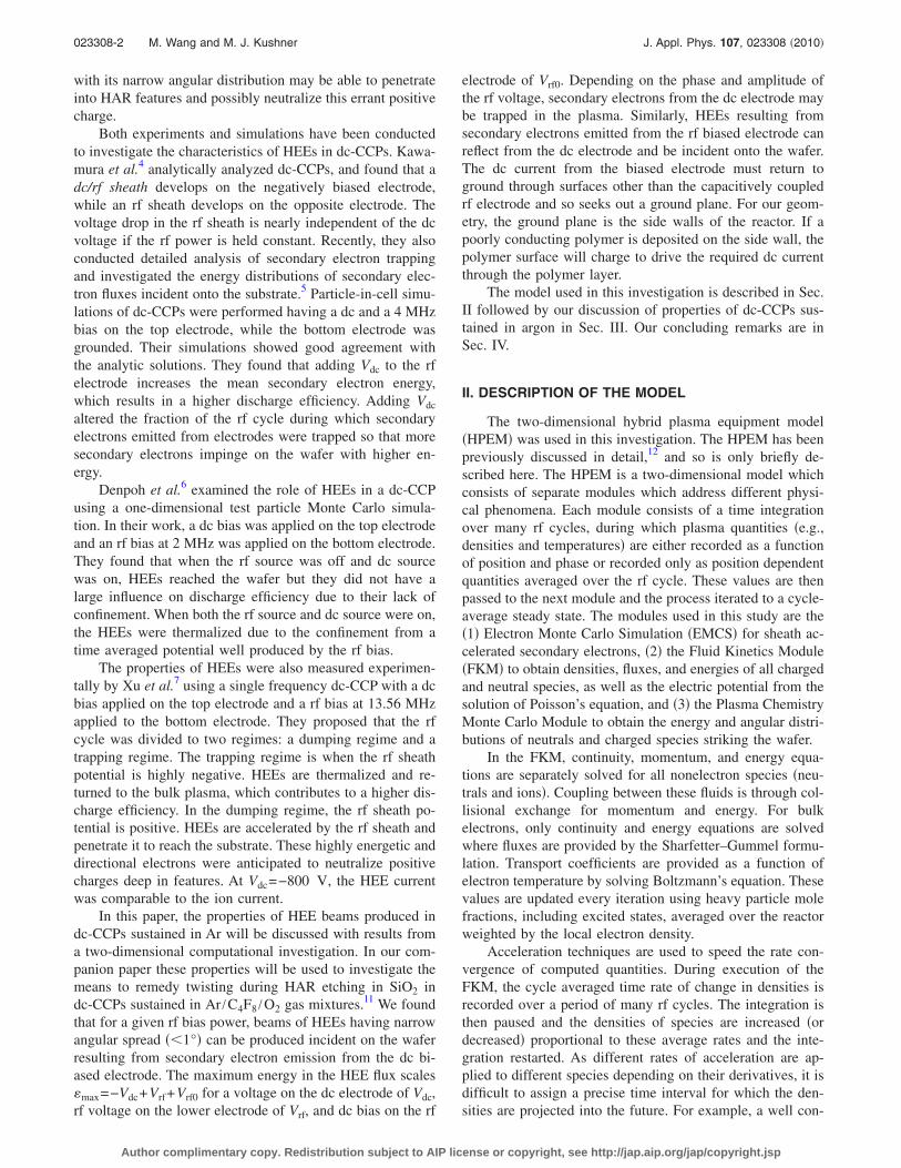
To investigate the proportion and distribution of HEEincident onto the wafer that originate from the rf electrodeand that have been reflected at least once by the dc sheath,the voltages and dc biases were fixed with Vrf=510 V, Vrf0
=−285 V, and Vdc=−520 V �conditions similar to the basecase�. The secondary emission coefficients for the wafer �rf
and top electrode �dc were then varied. The results for thenormalized energy distribution for the HEE flux to the waferare shown in Fig. 6�a�. The base case �denoted by �0� has�rf=�dc=0.15, and is compared to cases separately having�rf=0 and �dc=0. The high energy portion of the electronflux to the substrate is nearly indistinguishable for �rf=0.15and �rf=0. This indicates that the vast majority of the HEEflux for these conditions originates from the dc electrode.
When �dc=0, the flux dominantly consists of a low en-ergy peak contained below 100 eV. This represents electronsemitted from the substrate during that portion of the rf cyclewhen the voltage is increasing �becoming more positive�.Electrons accelerated by the rf sheath first cross the gap, arereflected by the dc sheath and return to the rf electrode whenthe sheath voltage is less negative. These electrons are able
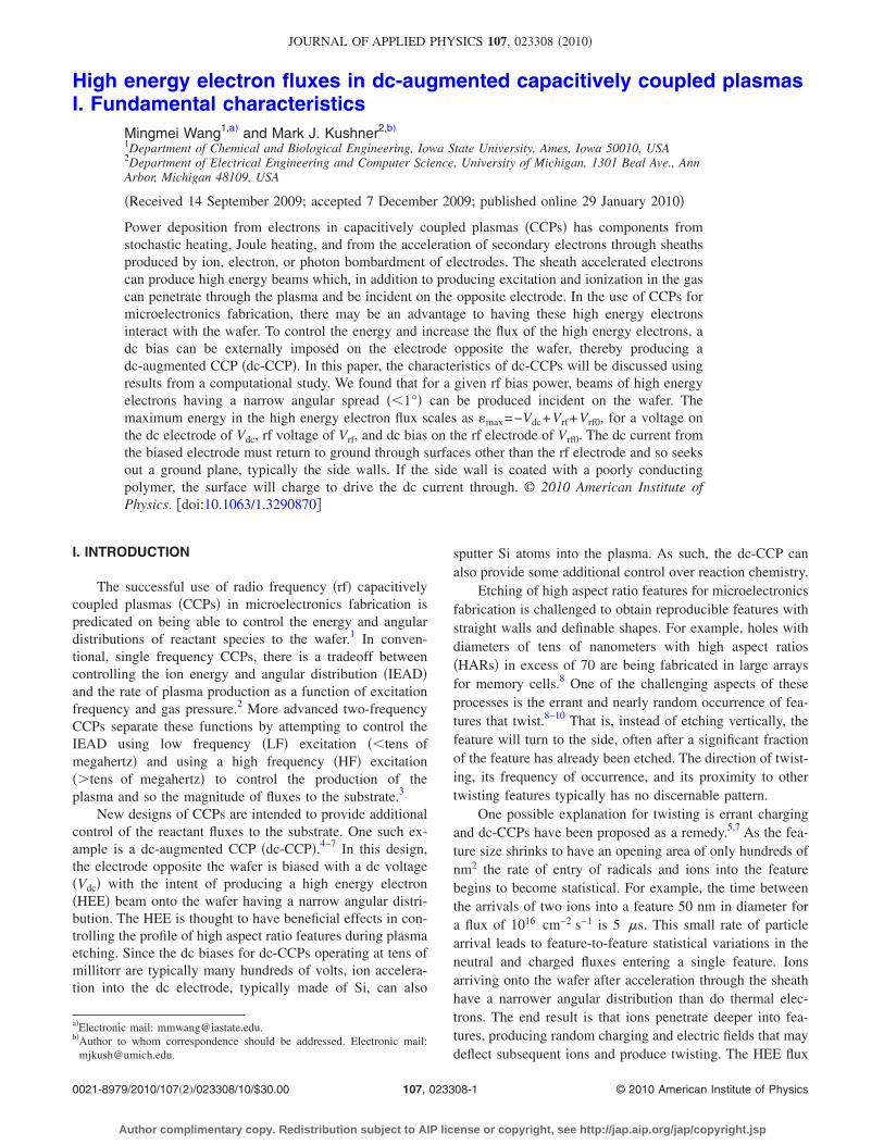
FIG. 5. �Color online� Plasma properties for Pdc=0 while varying the dcbias on the blocking capacitor on the rf electrode Vrf0. Vrf is held constant at510 V. �a� Plasma potential at different phases during the rf cycle for Vrf0
=−450 V. �b� EEDs for the HEE flux onto the wafer as a function of Vrf0.�c� Simulated results and theory for the maximum HEE energy as a functionof Vrf0
FIG. 6. �Color online� Energy and angular distributions for HEEs incidenton the electrode. �a� EEDs at different secondary emission coefficients ��0,��dc=�rf=0.15�; �dc=0.15, �rf=0; and �dc=0, �rf=0.15�. �b� Angular distri-butions for different �. The vast majority of the HEE flux about 100 eVresults from secondary emission from the dc electrode.
023308-6 M. Wang and M. J. Kushner J. Appl. Phys. 107, 023308 �2010�
Author complimentary copy. Redistribution subject to AIP license or copyright, see http://jap.aip.org/jap/copyright.jsp

to climb the sheath potential to reach the wafer. The energyof the collected HEE is approximately equal to the differencein the rf sheath potential over the time required for the HEEto make two gap crossings. Electrons emitted from the sub-strate during that portion of the rf cycle when the rf voltageis decreasing �becoming more negative� that cross the gapand are reflected by the dc sheath will also be reflected by therf sheath. This is because the rf sheath potential is morenegative after two gap crossing times than when the electronwas originally emitted. The electron is therefore not ener-getic enough to climb the instantaneous sheath potential. Thefluxes to the substrate with �rf=0 are diminished by about1/3 for energies �50 eV compared to �rf=0.15. This reduc-tion in flux is due to the absence of electrons emitted fromthe rf electrode which cross the gap, are reflected by the dcsheath, and collected by the wafer.
Since the ion fluxes to the electrodes change when � isvaried due to the change in the contribution of ionization byHEE, the magnitudes of the HEE fluxes produced by the ionfluxes also change. By normalizing the HEE fluxes by themagnitudes of the ion fluxes that produce them, the relativecontributions of electrons to the HEE flux onto the waferfrom the rf and dc electrodes can be determined. In doing so,we find that approximately 1/3 of the total HEE flux to thewafer �albeit dominantly below 100 eV� originates from sec-ondary emission from the rf electrode. The remainder �andthe vast majority at energies �100 eV� originates from sec-ondary emission from the dc electrode.
The angular distributions of HEEs incident on the waferare shown in Fig. 6�b�. With �rf=�dc=0.15 and �rf=0, theHEE flux is nearly fully contained within 0.5° of the vertical.Small asymmetries in angle result from two causes. The firstis curvature of the dc sheath due to the nonuniform plasmadensity across the upper electrode. This curvature generates asmall off-normal component to the electric field in the sheathwhich produces a non-normal trajectory. The second cause iselectric field enhancement at the edge of the rf electrode thatalso produces lateral components of the electric field in thesheath. For �dc=0, the majority of the HEE flux is also con-tained within 0.5° of the vertical; however, there is a broadbase to the angular distribution due to electrons collectedbelow 30 eV.
B. Collection of dc current
The dc augmentation on the upper electrode produces atime averaged dc current that must be returned to ground.Since the substrate is capacitively coupled it cannot pass atime averaged dc current, and so the current must seek an-other path to ground. In this particular geometry, the onlynondielectric covered surface �or only surface not capaci-tively coupled� is the metal side wall. �Recall that we pre-vented dc current from passing through the pump port bycovering it with a dielectric�. As a result, the dc current mustreturn to ground through the side wall.
For example, the rf cycle averaged magnitude of thecurrent density and current density vectors �showing direc-tion but not magnitude� are shown in Fig. 7 for Pdc=100 and300 W. This current density results from the ions and the
bulk electrons, but does not show the contribution of beamelectrons which at most would provide approximately � ofthe total at the electrode. The dc current density comes out ofthe side wall, converges through the gap at the edge of the dcelectrode as the radius decreases, and is dispersed along thesurface of the showerhead. The maximum current density of2.8 mA /cm2 for 100 W occurs midgap a few centimetersfrom the edge of the dc electrode. In order to drive thiscurrent, there is a small time averaged electric field from theelectrode to the side walls. The dc current density at 300 Wclosely resembles that of the 100 W case. The peak currentdensity of 4.2 mA /cm2 is less than twice that of the lowerpower. The increase in dc power is accomplished by increas-ing voltage �325 V for 100 W and 690 V at 300 W� aswell as by increasing the current density.
Although the capacitively coupled substrate must, on acycle averaged basis, pass no dc current, that requirementapplies only to the areal integral of the current density. Itdoes not apply locally if there is any significant surface con-ductivity. In this investigation, we allowed the wafer to havea finite conductivity �0.01 / cm� and so it is able to pass adc current in the radial direction. The end result is that thereis a small dc current that is collected at inner radii on thewafer and returned to the plasma at the outer radii while theareal integral is zero. �Had the substrate been a nonconduct-ing dielectric, the zero-current condition would have beenenforced locally as well as globally.� These dc current den-sities are small �peak values �0.1 mA /cm2� and are pro-duced by the plasma being nonuniform. In this case, theplasma has a maximum near the edge of the electrode whichproduces a higher electron beam current by secondary elec-tron emission from the dc electrode. This current is collectedon the edge of the wafer and so produces a positive currentinto the plasma. In this particular case, the recirculating cur-rent is largely attributable to the contributions of the HEEs tothe wafer. The recirculating current does not occur withPdc=0.
FIG. 7. �Color� The rf cycle averaged magnitude of the bulk electron andion current densities, and current density vectors for �a� Pdc=100 W and �b�Pdc=300 W. The maximum value for each case is noted. The vectors showdirection only �not magnitude�. A net current flows from the dc electrode tothe sidewalls.
023308-7 M. Wang and M. J. Kushner J. Appl. Phys. 107, 023308 �2010�
Author complimentary copy. Redistribution subject to AIP license or copyright, see http://jap.aip.org/jap/copyright.jsp

Plasma etching is often conducted in polymerizing gasmixtures which deposit polymer films on all surfaces in con-tact with the plasma. For example, Ar /C4F8 /O2 gas mixturesare used to etch dielectric materials such as SiO2.13 During afew-minute process, many to tens of microns of nominallypoorly conducting polymer may be deposited on the innersidewalls of the reactor. In conventional CCPs, the polymerdeposition is not particularly important from the vantagepoint of the circuit. The polymer layer is thin enough, and itscapacitance high enough, that rf current is not significantlyimpeded by the polymer. �Note that this polymer depositioncan change reactive sticking coefficients for radicals and socontribute to the seasoning or drift of reactors. See, for ex-ample, Ref. 14.� The deposition of polymer on the sidewallscould be problematic in dc-CCPs as the sidewall may be thelocation where the dc current returns to ground. The low-conducting nature of the polymer may impede the dc current.
To investigate the consequences of polymer depositionon the sidewalls in dc-CCPs, we added a layer of dielectricto the sidewall with a thickness of 3 mm and conductivity ofeither 0.1 / cm �high conductivity� or 10−5 / cm �low con-ductivity�. The dielectric constant of the polymer was ad-justed so that its capacitance would be similar to that of apolymer layer of a few hundred microns thickness. This ca-pacitance is high enough to pass the rf current unimpeded.The conditions are otherwise the same as the base case �Ar,40 mTorr, Prf=300 W, Pdc=200 W�. The cycle averagedplasma potential as a function of radius at the middle of thegap is shown for the low and high conductivity cases in Fig.8�a�. The high conductivity polymer is able to pass the dccurrent with a negligible voltage drop. In the low conductiv-ity case, the polymer charges to a negative potential, ap-proximately 20 V, to create a large enough electric field inthe polymer to drive the electron current through the polymerinto the sidewall. Since the metal sidewall is the referenceelectrode for the plasma potential, the time averaged plasmapotential is decreased by the amount of the voltage dropacross the polymer.
The resulting IEADs and EEDs incident onto the waferare shown in Fig. 8�b� for the high and low conductivitycases. The IEADs are nearly unchanged between the twocases. This is in part because the characteristics of the IEADsare determined by Vrf, Vrf0, and the rf current, all of whichare largely unaffected by the polymer on the sidewall sinceits capacitance is large enough to pass the rf current. Vrf
−Vrf0 increases from 810 to 820 V from the low to highconductivity cases. The maximum energy of the HEE de-creases by approximately 20 eV from the low to high con-ductivity case. There is a small 5 V increase �more negative�in Vdc to deliver Pdc=200 W, which might increase �max.However Vrf0 becomes more negative which then reduces�max.
To independently investigate the dependence of theHEEs and IEADs on the polymer sidewall coverage, Vrf �480V�, Vrf0 �285 V�, and Vdc �520 V� were held constant asopposed to adjusting them to deliver specified powers. Theseresulting distributions are shown in Fig. 8�c� for polymerconductivities of 0.1, 10−5, and 10−6 −1 cm−1. Since Vrf,Vrf0, and Vdc are constant, the HEEs are largely collisionless
and the HEEs traverse the gap in a small fraction of the rfperiod, the EEDs do not significantly change as the polymerconductivity changes. The IEADs incident on the substrateare, however, sensitive to the polymer conductivity. Al-though the average ion energy is independent of the polymerconductivity since Vrf and Vrf0 are the same, the shape of theIEAD reflects differences in the time dependence of the
FIG. 8. �Color online� Consequences of polymer deposition on the side-walls. �a� Cycle averaged plasma potential at the middle of the gap as afunction of radius. The polymer on the sidewall has conductivities of 0.1 and10−5 −1 cm−1. �b� Energy distributions of ions and HEE to the substrate forlow �10−5 −1 cm−1� and high �0.1 −1 cm−1� conductivity polymer. �c�Energy distributions of ions and HEE to the substrate for polymer conduc-tivities of 0.1, 10−5, and 10−6 −1 cm−1 at fixed bias voltages of Vrf
=480 V, Vrf0=−285 V, and Vdc=−520 V.
023308-8 M. Wang and M. J. Kushner J. Appl. Phys. 107, 023308 �2010�
Author complimentary copy. Redistribution subject to AIP license or copyright, see http://jap.aip.org/jap/copyright.jsp

plasma potential. With the lower conductivity polymer theplasma potential remains at its maximum value during thecathodic part of the rf cycle for a larger fraction of the cycle,and so the high energy peak of the IEAD is more prominent.
C. Two-frequency CCP
One implementation of the dc-CCP uses two rf frequen-cies: a low frequency �LF�10 MHz� on the substrate and ahigh frequency �HF�40–100 MHz� on the opposite dc bi-ased electrode. The goal of the two frequency excitationscheme is to separate ion acceleration, more efficiently pro-duced by the LF, from plasma generation, more efficientlyproduced by the HF. So given that in practice the amplitudeof the HF voltage VHF, is less than the magnitude of Vdc, thetop electrode becomes biased with an rf-modulated dc poten-tial.
To isolate the effects of adding a HF to the dc biasedelectrode, VLF �480 V� and Vrf0 �–285 V� on the lower elec-trode, and Vdc �–520 V� on the top electrode were held con-stant while VHF was varied. The LF is 5 MHz and the HF is40 MHz for 40 mTorr of argon. The EEDs incident onto thewafer resulting from secondary electron emission for VHF
=0, 150 and 300 V, are shown in Fig. 9. With VHF=0, theEED has a maximum energy of 715 eV, which correspondsto �max=−Vdc+VLF+Vrf0. The peak of the EED at �max resultsfrom the longer dwell time of the substrate bias at the maxi-
mum of the anodic cycle. With VHF=150 and 300 V, the dcbias is modulated on the top electrode with a sinusoidal VHF.The discrete peaks in the EED correspond to a full cycle ofmodulation of the dc voltage at the HF as the phase of the LFmore slowly changes. The maximum energy of the EEDshould be �max=−Vdc+VLF+Vrf0+VHF or 865 eV for VHF
=150 V and 1015 eV for VHF=300 V. The computed valuesare 853 and 993 eV. The lower computed values result fromthe finite crossing time across the gap of secondary electronsemitted from the dc electrode. In order to gain an energy�max, a secondary electron must be emitted at the maximumof the cathodic part of the HF cycle and strike the LF elec-trode at the maximum of its anodic cycle. In this example,the LF and HF have the same phase and the crossing timeacross the gap of a 1 keV electron is approximately 2 ns. Soduring the time between emission of the electron at the HFelectrode and it being collected at the LF electrode, the sub-strate voltage will have decreased by about 24 V, which ac-counts for the difference between the theoretical and com-puted values. The HEE distribution onto the substrate cantherefore be tuned to some degree by the phase differencesand frequencies of the LF and HF potentials.
D. Low frequency
In many applications of HAR etching, particularly indual frequency CCPs, the substrate bias is at frequencies aslow as 1–2 MHz. To investigate the consequences of thefrequency of the substrate bias on the EEDs incident on thewafer resulting from secondary electron emission, the sub-strate bias was varied between 2 and 16 MHz. Again, toisolate the effects of changing only the frequency of the sub-strate bias, Vrf �480 V� and Vrf0 �–285 V� on the lower elec-trode and Vdc �–520 V� on the top electrode were held con-stant. The resulting EEDs are shown in Fig. 10. On the scaleof the entire range of energies, the EEDs for frequencies of2–16 MHz are nearly indistinguishable. The high energypeak of the EED and the maximum electron energy do, how-ever, systematically vary. The peak and maximum energydecrease with increasing frequency. For a bias of 2 MHz, themaximum energy is 712 eV, which is nearly the same as themaximum theoretical energy of �max=−Vdc+Vrf+Vrf0 or 715eV. The maximum energy decreases to 702 eV at 16 MHz.This is in large part a transit time effect. In order for a sec-ondary electron to gain the maximum energy, it must beemitted from the dc biased electrode at the peak of the an-odic cycle and cross the electrode gap before the substratebias appreciably changes. The time required for a 700 eVelectron to cross the electrode gap is about 1.8 ns. Duringthis time, the voltage on the substrate near the peak of theanodic cycle at 16 MHz will have changed by 10 eV. Elec-trons emitted from the dc electrode on the ascending portionof the anodic cycle �bias becoming more positive� will gainenergy larger than that corresponding to the phase of theiremission because the substrate sheath potential is increasingduring its transit time. Electrons emitted at the peak anddescending portion of the rf cycle �bias becoming morenegative� will gain less energy, in this case about 10 eV at 16MHz.
FIG. 9. EEDs for HEE fluxes incident onto the wafer resulting from sec-ondary electron emission for a dual frequency dc-CCP. The values of VHF
are �top� 0, �middle� 150 and �bottom� 300 V. The other voltages �VLF
=480 V, Vrf0,=−285 V, Vdc=−520 V� were held constant. The HEE fluxonto the wafer is modulated by VHF displaced by the change in LF voltageduring the time the electron crosses the gap.
023308-9 M. Wang and M. J. Kushner J. Appl. Phys. 107, 023308 �2010�
Author complimentary copy. Redistribution subject to AIP license or copyright, see http://jap.aip.org/jap/copyright.jsp

IV. CONCLUDING REMARKS
Characteristics of HEE fluxes to the substrate were com-putationally investigated in single and dual frequency dc-CCPs. Electrons emitted from either the rf or dc electrodesare accelerated by the adjacent sheath and, if not degraded bycollisions, are incident on the opposite sheath. Depending onthe magnitude and phase of the rf sheath, the incident HEEfrom the dc electrode is either collected or reflected. HEEsfrom the dc electrode are collected with energies max�0,−Vdc−Vrf+Vrf0���s,� =−Vdc+Vrf+Vrf0. Even with Vdc=0,HEE fluxes as large as Vrf+Vrf0 can be collected by the wa-fer. Approximately 30% of the HEE flux collected by the
wafer, mostly at energies �100 eV, can be attributed to sec-ondary electrons emitted by the rf biased substrate and re-flected by the dc sheath. The current emitted by the dc elec-trode must return to ground through a noncapacitivelycoupled surface. In our model, that surface is the groundedsidewall. When the sidewall is coated with a poorly conduct-ing polymer, charge will build up to push the dc currentthrough the coating. This could result in sparking under ex-treme conditions. When applying a HF bias to the dc elec-trode in a dual frequency CCP, the HEE flux is modulated bythe HF voltage. The precise energy spectrum of the HEE fluxcollected by the substrate then depends on the relative phasesof the LF and HF biases. The HEE distribution onto thesubstrate can therefore be tuned to some degree by the phasedifferences and frequencies of the LF and HF potentials. Theconsequences of HEE fluxes on etching of high-aspect-ratioSiO2 features using fluorocarbon plasmas are discussed inour companion paper.11
ACKNOWLEDGMENTS
This work was supported by Tokyo Electron Ltd., theSemiconductor Research Corp., and Micron Corp.
1S.-B. Wang and A. E. Wendt, J. Appl. Phys. 88, 643 �2000�.2T. Novikova, B. Kalache, P. Bulkin, K. Hassouni, W. Morscheidt, and P.Roca i Cabarrocas, J. Appl. Phys. 93, 3198 �2003�.
3T. Kitajima, Y. Takeo, Z. Lj. Petrovic, and T. Makabe, Appl. Phys. Lett.77, 489 �2000�.
4E. Kawamura, M. A. Lieberman, A. J. Lichtenberg, and E. A. Hudson, J.Vac. Sci. Technol. A 25, 1456 �2007�.
5E. Kawamura, A. J. Lichtenberg, and M. A. Lieberman, Plasma SourcesSci. Technol. 17, 045002 �2008�.
6K. Denpoh and P. L. G. Ventzek, J. Vac. Sci. Technol. A 26, 1415 �2008�.7L. Xu, L. Chen, M. Funk, A. Ranjan, M. Hummel, R. Bravenec, R.Sundararajan, D. J. Economou, and V. M. Donnelly, Appl. Phys. Lett. 93,261502 �2008�.
8S. Welch, K. Keswick, P. Stout, J. Kim, W. Lee, C. Ying, K. Doan, H. S.Kim, and B. Pu, Semicond. Int. 32, 18 �2009�.
9M. Kiehlbauch, “Reverse masking profile improvements in high aspectratio etch,” U.S. Patent Application No. 2009/7553770 �2009�.
10J. Bing, E. A. Edelberg, and T. Yanagawa, “Reducing twisting in ultra-high aspect ratio dielectric etch,” U.S. Patent Application No. 2008/0119055 �2008�.
11M. Wang and M. J. Kushner, J. Appl. Phys. 107, 023309 �2010�.12M. J. Kushner, J. Phys. D 94, 194013 �2009�.13X. Li, L. Ling, X. Hua, M. Fukasawa, G. S. Oehrlein, M. Barela, and H.
M. Anderson, J. Vac. Sci. Technol. A 21, 284 �2003�.14B. Zhou, E. A. Joseph, S. P. Sant, Y. Liu, A. Radhakrishnan, L. J. Overzet,
and M. J. Goeckner, J. Vac. Sci. Technol. A 23, 1657 �2005�.
FIG. 10. �Color online� EEDs for HEE fluxes incident onto the wafer re-sulting from secondary electron emission while varying the frequency of thebias on the lower electrode. �a� Full energy range and �b� expansion of scaleat high energy. The voltages �Vrf=480 V, Vrf0=−285 V, and Vdc=−520 V�were held constant. The HEE flux onto the wafer is not significantlychanged by the bias frequency though the maximum energy decreases by afew electron volts at high energy due to the finite cross time of secondaryelectrons.
023308-10 M. Wang and M. J. Kushner J. Appl. Phys. 107, 023308 �2010�
Author complimentary copy. Redistribution subject to AIP license or copyright, see http://jap.aip.org/jap/copyright.jsp