homework 3 ece 6414 by asma beevi k t, badarish colathur...
TRANSCRIPT

Homework 3
ECE 6414
By
Asma Beevi K T, Badarish Colathur Arvind and Nithanth B S
(Group 4)

Problem 1 The following is the schematic of the desired op-amp. The sizing of the added diode connected transistor (M37) is found as 100n/500n = 10/50.
The DC gain for the above op-amp topology is shown below for various values of VDD (0.7 to 1 V)

The large signal step responses are shown below:
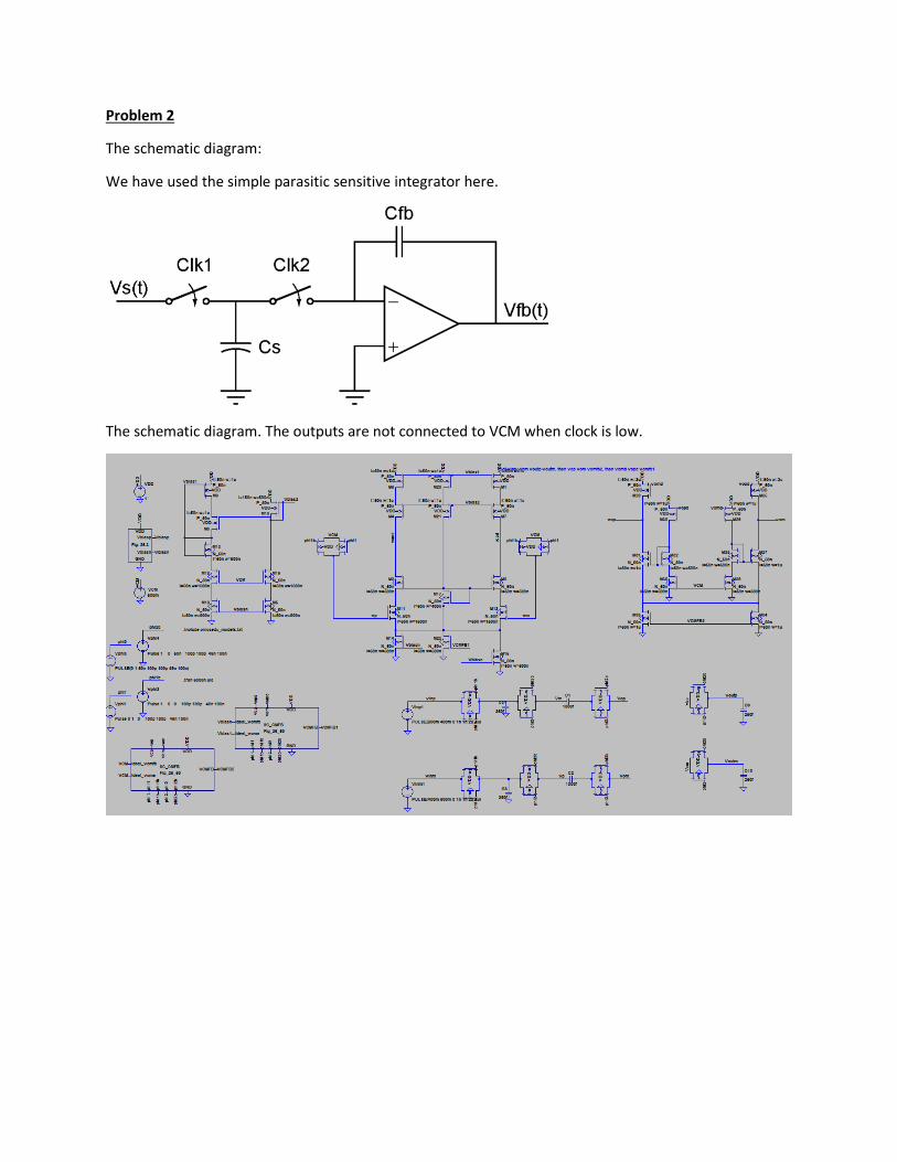
Problem 2
The schematic diagram:
We have used the simple parasitic sensitive integrator here.
The schematic diagram. The outputs are not connected to VCM when clock is low.

Simulation results:
Simulation output for a square wave input
Simulation output for a sinusoidal input.
We can see that the common mode level is close to 0.5 V

Problem 3
The circuit from Fig 27.17 is implemented here in the short channel process. Every Pmos is of 1u/50n,
and Nmos of 500n/50n.

Here the input slew rate was 2V/ns.
The delay when the input rises is 87ns and when the input falls is 95ns.
On changing the input slew to 0.2V/ns this is what we get.
When the input is falling the delay is 160ns and when the input rises it is still 90ns.
This shows that the rise times remain fairly constant but the fall time nearly doubled.
Hence the output rise and fall delays are sensitive to input slew rate and are not very symmetrical.
In order to reduce the power consumption of the buffer, it is advisable to convert M6 and M7 to longer
channels.

We changed M6 and M7 from 10/1 to 10/4.
Below it the comparison of current drained through M7 in the original circuit and longer channel M7
when the slew rate was 2V/ns.
The current reduction is nearly 50%.
However the output delay and skew increases.
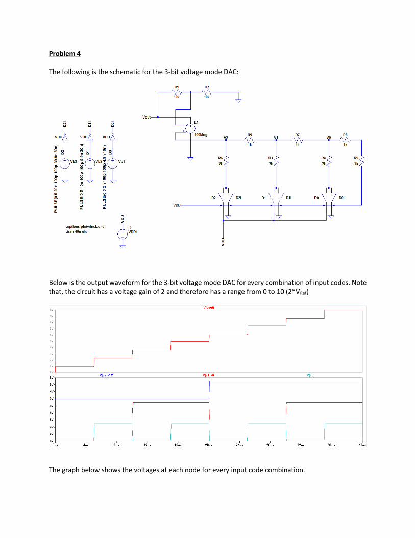
Problem 4 The following is the schematic for the 3-bit voltage mode DAC:
Below is the output waveform for the 3-bit voltage mode DAC for every combination of input codes. Note that, the circuit has a voltage gain of 2 and therefore has a range from 0 to 10 (2*VRef)
The graph below shows the voltages at each node for every input code combination.


Problem 5 The output voltage at the end of nth cycle of the conversion with feedback amplifier gain of 0.5V/V is given below:
The output voltage at the end of nth cycle of the conversion with feedback amplifier gain of 0.45V/V will have the gain 0.5V/V replaced by 0.45V/V
The table below summarizes the resultant output voltage for different inputs. Note that, the outputs are the final outputs (at the end of 3 cycles) for every digital input combination.
INPUT D2 D1 D0 Vout (Gain = 0.5V/V)
Vout (Gain = 0.45V/V)
0 0 0 0 0 0
1 0 0 1 0.625 0.4556525
2 0 1 0 1.25 1.0125
3 0 1 1 1.875 1.468125
4 1 0 0 2.5 2.25
5 1 0 1 3.125 2.705625
6 1 1 0 3.75 3.2625
7 1 1 1 4.375 3.718125

GAIN ERROR –
(𝑦2−𝑦1
𝑥2−𝑥1)
𝑟𝑒𝑑− (
𝑦2−𝑦1
𝑥2−𝑥1)
𝑏𝑙𝑢𝑒
(
78
𝑉𝑟𝑒𝑓 − 0
78
𝑉𝑟𝑒𝑓 − 0)
𝑟𝑒𝑑
− (3.718125 − 0
78
𝑉𝑟𝑒𝑓 − 0)
𝑏𝑙𝑢𝑒
GAIN ERROR = 1 – 0.85 = 0.15 V/V

Problem 6


Problem 7 The voltage on the i-th tap of the resistor string in case of resistor-string DAC was found to be:
Similar analysis can be applied to the resistor string in the Flash ADC resulting in the same expression as the one shown above.
Resistor Mismatch(%) R ΔR Dout Vin,actual (V)
Vin,ideal (V) INL (mV)
DNL(mV)
1 2 1.02 0.02 0 0 0 0 -
2 1.5 1.015 0.015 1 0.3172 0.3125 4.7 4.61
3 0 1.000 0.000 2 0.6328 0.6250 7.8 0.00
4 -1 0.99 -0.010 3 0.9437 0.9375 6.2 -3.16
5 -0.5 0.995 -0.005 4 1.2516 1.2500 1.6 -1.57
6 1 1.01 0.01 5 1.5609 1.5625 -1.6 3.09
7 1.5 1.015 0.015 6 1.8750 1.8750 0.0 4.62
8 2 1.02 0.02 7 2.1906 2.1875 3.1 6.127
9 2.5 1.025 0.025 8 2.5078 2.5000 7.8 7.622
10 1 1.01 0.01 9 2.8265 2.8125 14.0 3.094
11 -0.5 0.995 -0.005 10 3.1405 3.1250 15.5 -1.57
12 -1.5 0.985 -0.015 11 3.4499 3.4375 12.4 -4.759
13 -2 0.98 -0.02 12 3.7562 3.7500 6.2 -6.378
14 0 1.000 0.000 13 4.0609 4.0625 -1.6 0.00
15 1 1.01 0.01 14 4.3719 4.3750 -3.1 3.094
16 1 1.01 0.01 15 4.6859 4.6875 -1.6 3.094
In this problem, we are assuming that the comparator is ideal and thus does not have any offset voltage. For a comparator to be considered as N-bit effective, it should satisfy the following condition:
𝑀𝑎𝑥(𝐼𝑁𝐿, 𝐷𝑁𝐿) < 0.5 ∗ 𝐿𝑆𝐵 We also know that 0.5*LSB = Vref /(2N+1) = 5/32 = 0.15625.
𝑀𝑎𝑥(𝐼𝑁𝐿, 𝐷𝑁𝐿) = 𝐼𝑁𝐿 = 0.0155 Therefore, 𝑀𝑎𝑥(𝐼𝑁𝐿, 𝐷𝑁𝐿) < 0.15625 and therefore the 4 bit flash ADC in the problem has 4 bits of resolution.

Problem 8

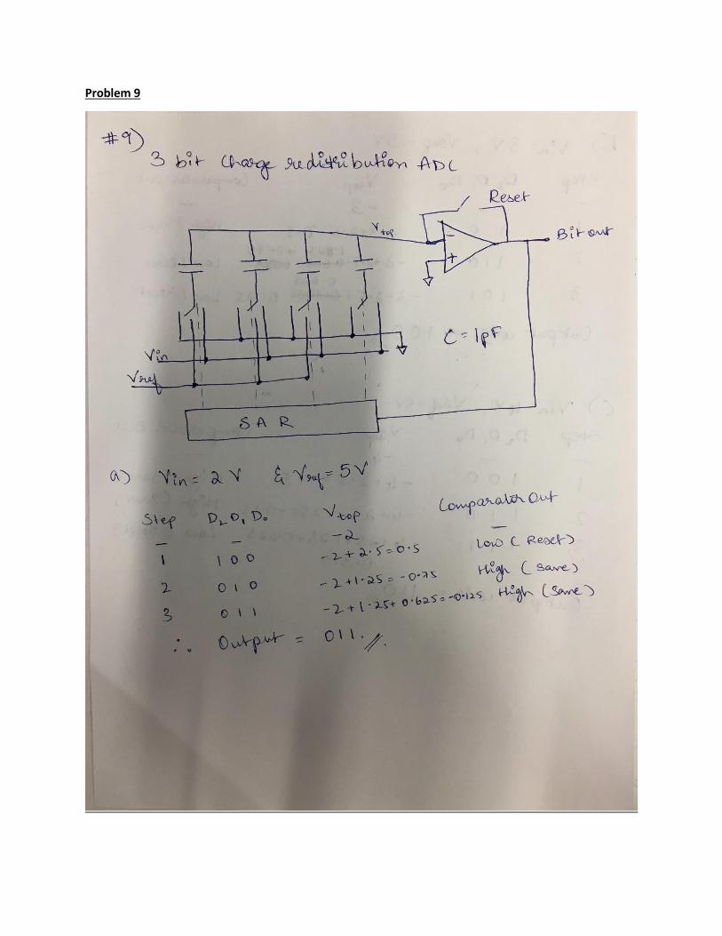
Problem 9


Problem 10
