hybrid dual full-bridge dc-dc converter with reduced circulating ... · ipril(t) = o.snlo +...
TRANSCRIPT
Hybrid Dual Full-Bridge DC-DC Converter with Reduced Circulating Current, Output Filter
and Conduction Loss of Rectifier Stage for RF Power Generator Application
Young-Do Kim I1-0un Lee, In-Ho Cho and Gun-Woo Moon Samsung Electro-Mechanics
Su-won, Korea
Abstract- In this paper, a hybrid dual full-bridge DCDC converter for radio-frequency (RF) power generator application is proposed to overcome the drawbacks of conventional phase-shift full-bridge (PSFB) converter such as large circulating current of primary side and large output filter size. The proposed converter adopts dual full-bridge hybrid structure with a small series capacitor in the primary side and full-bridge rectifier with two additional low-voltage-rated diodes in the secondary side. With this structure, the proposed converter has advantages of reduction of circulating current, zero-voltage switching (ZVS) operation of all primary switches, size reduction of output inductor, and low conduction loss of rectifier stage. Furthermore, the proposed converter can regulate the output voltage very wide by changing the operational mode according to the output voltage. These advantages result in the improvement of whole load efficiency. The operational principle and analysis of proposed converter are presented and analyzed. A 3kW 40-200V output laboratory prototype is designed and built to verify the feasibility and the effectiveness of the proposed converter.
Index Terms- Hybrid dual full-bridge, Output filter, Circulating current, Zero-voltage switching (ZVS), Wide output voltage applications
I. INTRODUCTION
Conventional phase-shift full-bridge (PSFB) converter is attractive topology for the high-power and wideoutput-voltage applications, since it has some desirable features such as low current/voltage stress, ZVS operation of all primary switches and variable output regulation capability by the phase-shifted control signal [1]
However, the conventional PSFB converter has several problems for wide-output-voltage applications such as RF power generator. Since the operating duty cycle of the conventional PSFB converter extremely varies with the output voltage variation, large circulating current exists on primary side during freewheeling period [3 - 6]. Beside of that, the size of output filter is highly increased due to the small duty operation and it results in low power density and high cost [7-10]. Furthermore, for the high-power and high-output-voltage applications, transformer of the conventional PSFB converter has high turns-ratio so that the primary conduction loss of the conventional PSFB converter is highly increased and the high-voltage-rated diode, which generally has high conduction loss and poor performance such as reverserecovery property, has to be employed for the secondary side [10].
978-1-4799-0482-2/13/$31.00 ©2013 IEEE 176
KAIST
Dae-jeon, Korea
To solve these problems, a hybrid dual full-bridge converter with reduced circulating current, small output filter, and low conduction loss of rectifier stage for RF power generator applications is proposed in this paper.
II. DESCRIPTION OF PROPOSED CIRCUIT
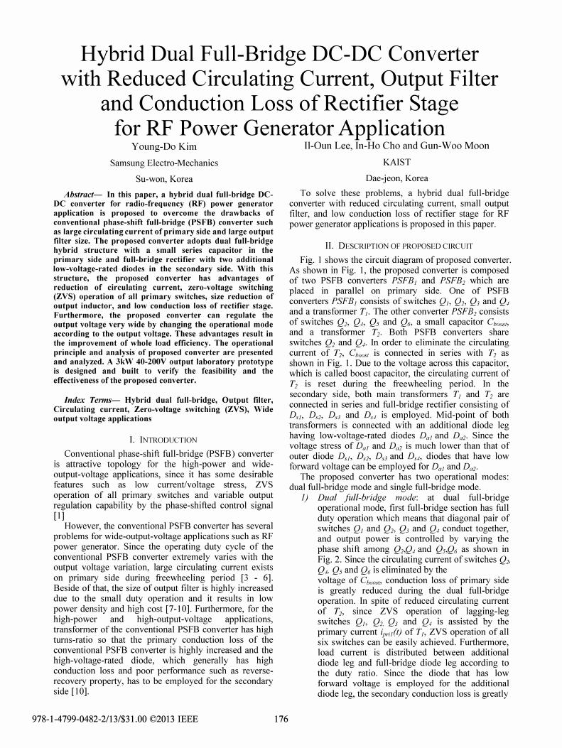
Fig. 1 shows the circuit diagram of proposed converter. As shown in Fig. 1, the proposed converter is composed of two PSFB converters PSFBI and PSFB2 which are placed in parallel on primary side. One of PSFB converters PSFBI consists of switches Ql, Q2, Q3 and Q� and a transformer TI• The other converter PSFB2 consists of switches Q}, Q�, Q5 and Q6, a small capacitor Ch()O\(, and a transformer T2• Both PSFB converters share switches Q2 and Q4. In order to eliminate the circulating current of T2, Cboosl is connected in series with T2 as shown in Fig. 1. Due to the voltage across this capacitor, which is called boost capacitor, the circulating current of T2 is reset during the freewheeling period. In the secondary side, both main transformers TI and T2 are connected in series and full-bridge rectifier consisting of Dsh Ds2, Ds3 and Ds4 is employed. Mid-point of both transformers is connected with an additional diode leg having low-voltage-rated diodes Dol and Do2. Since the voltage stress of Dol and Da2 is much lower than that of outer diode D,], Ds2, Ds3 and D,4, diodes that have low forward voltage can be employed for Dol and Do2'
The proposed converter has two operational modes: dual full-bridge mode and single full-bridge mode.
1) Dual full-bridge mode: at dual full-bridge operational mode, first full-bridge section has full duty operation which means that diagonal pair of switches QI and Q2, Q3 and Q4 conduct together, and output power is controlled by varying the phase shift among Q2,Q4 and Q5,Q6 as shown in Fig. 2. Since the circulating current of switches Q2. Q4. Q5 and Q6 is eliminated by the voltage of Cho()Sb conduction loss of primary side is greatly reduced during the dual full-bridge operation. In spite of reduced circulating current of T2, since ZVS operation of lagging-leg switches Ql, Q2, Q3 and Q4 is assisted by the primary current ipril(t) of Th ZVS operation of all six switches can be easily achieved. Furthermore, load current is distributed between additional diode leg and full-bridge diode leg according to the duty ratio. Since the diode that has low forward voltage is employed for the additional diode leg, the secondary conduction loss is greatly
0" 0"
T, Co Ro 0" 0"
: •••• __________ J Fig. I Circuit diagram of proposed converter
reduced. 2) Single full-bridge mode: at single full-bridge
operational mode, phase-shifted gate signal is applied to switches Q/, Q], Q3 and Q�. , and switches Q5 and Q6 are disenabled as shown in Fig 3. Hence, power is mainly delivered to the output stage through Q], Q2, Q3, Q4, h Dslo D<], Do] and Do2' Since TI of the proposed converter has lower turns-ratio than that of the conventional PSFB converter, full-bridge stage can be operated with large duty ratio and it results in reduction of conduction loss in primary side. Furthermore, since main power is delivered through Do] and Da2, which have low forward voltage, secondary conduction loss is also reduced during the single full-bridge operation.
Since the proposed converter has to provide variable output voltage according to the output power variation in RF power generator applications, boundary of mode change between single full-bridge operation and dual fullbridge operation can be decided by the design of turnsratio of both transformers TI and T2.
I I I. OPERATIONAL PRINCIPLE
For the analysis of proposed converter, several assumptions are made as follows:
1) All switches are ideal except for the output capacitor Coss and the internal anti-parallel diode of it.
2) All rectifier diodes are ideal. 3) The output inductor L() is large enough to be
considered as a constant current source 10 during a switching period.
4) The magnetizing inductance Lm2 of transformer T2 is large enough to ignore the effect of the
5) Magnetizing current during switching period, while the magnetizing inductance Lm 1 of transformer T] is designed with small value.
6) Two transformers TI and T2 have same turns-ratio of n] =Ns/Np] =n2=N,/Np2 and n=n]+n2'
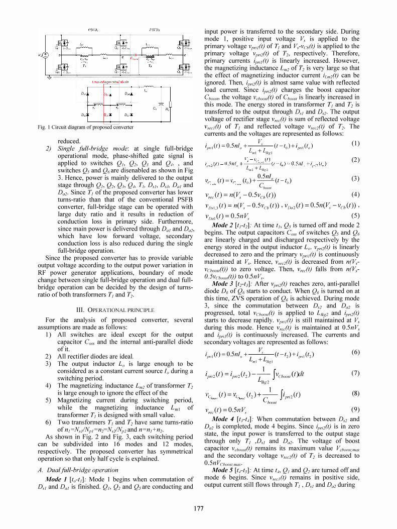
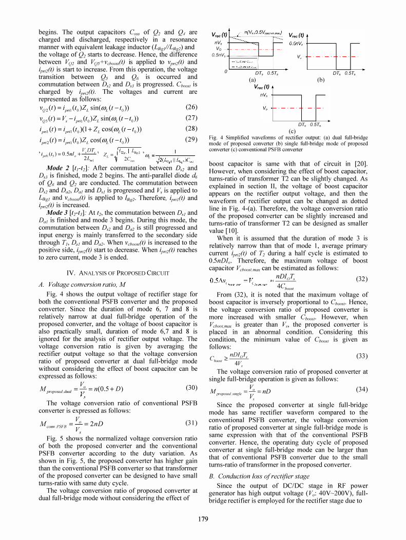
As shown in Fig. 2 and Fig. 3, each switching period can be subdivided into 16 modes and 12 modes, respectively. The proposed converter has symmetrical operation so that only half cycle is explained.
A. Dual full-bridge operation Mode 1 [to-til' Mode 1 begins when commutation of
D,] and Da] is finished. Qlo Q2 and Q5 are conducting and
177
input power is transferred to the secondary side. During mode 1, positive input voltage Vs is applied to the primary voltage Vpril( t) of TI and V,-VCh( t) is applied to the primary voltage Vpri2(t) of T2, respectively. Therefore, primary currents ipri l( t) is linearly increased. However, the magnetizing inductance Lm2 of T2 is very large so that the effect of magnetizing inductor current irm 2( t) can be ignored. Then, ipri 2(t) is almost same value with reflected load current. Since ipri 2( t) charges the boost capacitor Cboos!, the voltage VCboos/ t) of Cboos! is linearly increased in this mode. The energy stored in transformer TI and T2 is transferred to the output through Ds] and D,2' The output voltage of rectifier stage vreJt) is sum of reflected voltage vsecl t) of T] and reflected voltage Vsec2(t) of T2. The currents and the voltages are represented as follows:
V iprtl(t) = O.Snlo + S (t-to)+ipril(to) Lml + L'kgl
V -v' (t) ip,n(t)=O.5nl,,+ ·' c,'" (t-to)�O.5nlo+ip,n(tJ
L/Il2 + L1kg2 (1)= O.5n1o ) (lo)+-- (l-to
ChoOSI VrecCt)= nCV, -O.5VChCt))
(1)
(2)
(3)
(4)
VDsl,3 (t) = nCVs - O.5vCb (t)) , VDa2 (t) = O.5n(V, -VCb (t)) ,
Vf)Ol(t)= O.5nV, (5) Mode 2 [trt2]: At time t/, Q5 is turned off and mode 2
begins. The output capacitors Coss of switches Q5 and Q6 are linearly charged and discharged respectively by the energy stored in the output inductor La. Vpri2(t) is linearly decreased to zero and the primary Vpril( t) is continuously maintained at VS' Hence, Vsec2(t) is decreased from n(V ,VCh()()s/t)) to zero voltage. Then, vreJt) falls from n(V.,O.5VCboos/t)) to O.5n Vs.
Mode 3 [trt3]: After Vpri2( t) reaches zero, anti-parallel diode D6 of Q6 starts to conduct. When Q6 is turned on at this time, ZVS operation of Q6 is achieved. During mode 3, since the commutation between D,2 and Da2 is progressed, total vCho() ,lt) is applied to L 'kx 2 and ipri 2(t) starts to decrease rapidly. vpru(t) is still maintained at Vs during this mode. Hence vreJt) is maintained at O.5n V, and ipru(t) is continuously increased. The currents and secondary voltages are represented as follows:
V ipril (t) = O.5n1o + s (t - tJ + ipril (tJ
Lml + L'kgl
ipri2(t) = ipri2(t2) -f- fVCboosJt)dt Ikx2
(t) = 1 f' (t2)+ -- lpri2(t) Chaos!
VrecCt) = O.5nV,
(6)
(7)
(8)
(9)
Mode 4 [trt4]: When commutation between Ds2 and Do2 is completed, mode 4 begins. Since ipri 2(t) is in zero state, the input power is transferred to the output stage through only T] ,D,] and Do2. The voltage of boost capacitor Vch()os/ t) remains its maximum value Veho()s/,mox and the secondary voltage Vsec 2( t) of T2 is decreased to O.5n VCho()si.max.
Mode 5 [trt5]: At time t4, Q] and Q2 are turned off and mode 6 begins. Since v,eelt) remains in positive side, output current still flows through T] , D,] and Da2 during

T, DT,
� �' =====Q�,�--' Q,
Fig. 2 Key waveform at dual-full bndge operatIOn
this mode. Hence, Coss of Q], Q2, Q3 and Q4 are linearly charged and discharged respectively by the reflected load current of TI and the current of magnetizing inductor Lml. The voltages and currents are represented as follows: ipril ( t) = O.Snlo + ILm1(t4) (10)
vQ3 (t) = vQ4 (t) = v: O.Snlo+lr.ml(t4)(t_t4) ( 11 )
4Coss
Ct) = V O.Snlo + 11.",1 (t4) (t-t ) Vpri1 s
2eoss 4 (12)
( ) --V O.SnIO +11.ml(t4) (t-t ) (13)
Vpri2 t - Choost.max 4Coss 4
Mode 6 [t5-t6]: When the sum of vseclt) and Vsec2( t) reaches at zero voltage, mode 6 starts. At time t5, D,4 starts to conduct and commutation between Dsl and Ds4 is progressed. The Coss of Q I, Q2, Q3 and Q4 are charged and discharged, respectively in a resonance manner with Llkxl+Llkx2. The voltages and currents are represented as follows:
v pril (t) = vpril (tJ - 2ipril (ts )Zo sine OJo (t -ts)) (14)
V pril (t) = Vpril (tS) - 2ipril (tS )Zo sine OJo (t -ts)) ipril (t) = ipril (ts )(1- Zo cos( OJo (t -ts)) ipriz(t) = -ipril(ts)Zo cos(OJo(t -ts))
(1S)
(16)
(17)
, V T , Z = LlkKI + LZkK2 , T., -r====== Zpn1Ct,)= 05nI"+-'-' � 4Lml " 4C" •. , 0 �4(Llkgl + L1kg2)C"."
Mode 7 [t6-t7]: After vpru(t) and Vpri2(t) reach -V" antiparallel diode D3 of Q3 and anti-parallel diode D4 of Q4 start to conduct. When Q3 and Q4 are turned on at this time, ZVS operation of Q3 and Q4 is achieved. During this mode, the commutation between Dsl and Ds4 is still progressed. The sum of the input voltage V, and divided voltage of Vcboosl.max is applied to both leakage inductor L1kxl of TI and leakage inductor L1kx2 of T2 so that ipru(t) and ipri2( t) is rapidly decreased to negative side. The voltages and currents are represented as follows:
178
T,
� ��l ==DT=, ""0:=, =+----, ,------ro', __ ---ji ['(5;
Vprl1
W
0, I
! i • cooo"
! � I!
0, 0,
I� I i
\1 Ipri1
Ipri2
- ��----;/"""""" �
r io i loa2-..,
... +Vos2,Da1 : I O. 5n v, ! ! I , ; i l
\� i i Joa1--..
1
Fig. 3 Key waveform at smgle full-bndge operatIOn
L[kgl V,lkgl = V, + VCboostmax L + L Ikg1 Ikg2
1
IX
r
(18)
L[kg2 (19) V,,,g2 = V, + VCbomfmax L + L Ik"1 Ik"2 V
' Ct)-' .Ct )-�(t-t ) (20) Ipnl -I1'n1 G L 6
lkgl
i . (t) = - V,'/kg2 (t-t ) (21) pn2. L 2
Ikx2 Mode 8 [trt8]: When commutation between Dsl and
Ds4 is finished, mode 8 begins. At this time, since commutation between Ds3 and Da2 is progressed, 1Is is applied to the L1kxl and ipru(t) is continuously decreased to the negative side. The negative voltage -V,+vcboosl t) is applied to Vpri2( t), then vrel t) is increased to O. Sn(V, +vcboosl t)) and input energy is transferred to the output through T2, Q4, Q6, Da2 and D,4' The voltages and currents are represented as follows: . . VI (22) l1'ril (t) = l1'ril (t7) ---z-Ct -t7)
lkgl
B. Single full-bridge operation
(23)
(24)
(2S)
The operation of the proposed converter at single fullbridge operation is almost same with conventional PSFB converter except Mode I, 2 and 3. Hence, only Mode 1, 2 and 3 are explained and the explanation of other modes is omitted.
Mode 1 [to-tl]: At to, after Q4 is turned off and mode 1
begins. The output capacitors Coss of Q2 and Q� are charged and discharged, respectively in a resonance manner with equivalent leakage inductor (Llkg/ILlkg2) and the voltage of Q2 starts to decrease. Hence, the difference between VQ2 and VQ5+Vchoosl t) is applied to Vpri2(t) and ipri2(t) is start to increase. From this operation, the voltage transition between Q5 and Q6 is occurred and commutation between Ds2 and Ds3 is progressed. Cbaost is charged by ipri2(t). The voltages and current are represented as follows:
vQ2(t) = ipril (ta)ZL sin({OL (t -ta))
vQs(t) = V, - ipriJ(to)Zr sin({Or(t- to))
ipril (t) = ipril (to)(l + ZL COS({OL (t -to))
ipri2 (t) = ipriJ (to )ZJ cos( {OJ (t -to)) �--
(26)
(27)
(28)
(29)
, . (t ) = O.5nl + V,DT" z L'legl ll L'kg2 , lpnl ::, 0 2L T. = lOr, --;====c=::'= ",I 2C"." �2(Llkgl II L,kg2)C""
Mode 2 [trt2]: After commutation between Ds2 and Dd is finished, mode 2 begins. The anti-parallel diode d6 of Q6 and Q2 are conducted. The commutation between D,2 and Dab Dol and D,l is progressed and V, is applied to L1kgJ and vchooslt) is applied to Ilkg2. Therefore, ipril( t) and ipri2(t) is increased.
Mode 3 [trt3]: At t2, the commutation between D.d and Dal is finished and mode 3 begins. During this mode, the commutation between D'2 and Do2 is still progressed and input energy is mainly transferred to the secondary side through TJ, D,J and Da2. When Vchool/t) is increased to the positive side, ipri2(t) start to decrease. When ipri2(t) reaches to zero current, mode 3 is ended.
IV. ANALYSIS OF PROPOSED CIRCUIT
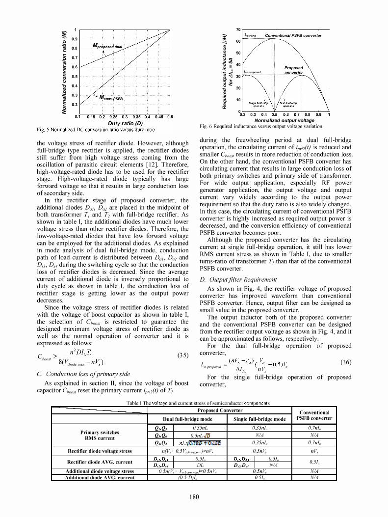
A. Voltage conversion ratio, M Fig. 4 shows the output voltage of rectifier stage for
both the conventional PSFS converter and the proposed converter. Since the duration of mode 6, 7 and 8 is relatively narrow at dual full-bridge operation of the proposed converter, and the voltage of boost capacitor is also practically small, duration of mode 6,7 and 8 is ignored for the analysis of rectifier output voltage. The voltage conversion ratio is given by averaging the rectifier output voltage so that the voltage conversion ratio of proposed converter at dual full-bridge mode without considering the effect of boost capacitor can be expressed as follows:
V M - --.!!... - n(O 5+D) proposed.dual - v. -
. . ,
(30)
The voltage conversion ratio of conventional PSFB converter is expressed as follows:
MCOI1VPSFH = Vo
= 2nD (31) Vs
Fig. 5 shows the normalized voltage conversion ratio of both the proposed converter and the conventional PSFS converter according to the duty variation. As shown in Fig. 5, the proposed converter has higher gain than the conventional PSFS converter so that transformer of the proposed converter can be designed to have small turns-ratio with same duty cycle.
The voltage conversion ratio of proposed converter at dual full-bridge mode without considering the effect of
179
Vrec (t) f<,·c::,.·· .. · .............. · .. · .......... · .. · .. ·· .......... ··r.·":� .. n v, -f----""'-= Va
O. 5nV, 4====::;t"-"""1 o DT, O.5T,
(a)
Vrec (t) O.5nV,,-+-----,
DT, O.5T, (b)
Vrec{t) nV,-+-----,
DT, O.5T, (c)
Fig. 4 Simplified waveforms of rectifier output: (a) dual full-bridge mode of proposed converter (b) single full-bridge mode of proposed converter (c) conventional PSFB converter
boost capacitor is same with that of circuit in [20]. However, when considering the effect of boost capacitor, turns-ratio of transformer T2 can be slightly changed. As explained in section II, the voltage of boost capacitor appears on the rectifier output voltage, and then the waveform of rectifier output can be changed as dotted line in Fig. 4-(a). Therefore, the voltage conversion ratio of the proposed converter can be slightly increased and turns-ratio of transformer T2 can be designed as smaller value [10].
When it is assumed that the duration of mode 3 is relatively narrow than that of mode 1, average primary current ipri2( t) of T2 during a half cycle is estimated to O.5nDlo. Therefore, the maximum voltage of boost capacitor Vcbaosl.max can be estimated as follows:
nDl ()T, --- (32) 4Cboost
From (32), it is noted that the maximum voltage of boost capacitor is inversely proportional to Cboasi' Hence, the voltage conversion ratio of proposed converter is more increased with smaller Chowt' However, when Vcboat.max is greater than V" the proposed converter is placed in an abnormal condition. Considering this condition, the minimum value of Cbaost is given as follows:
nD1oT, CbOOSI;:::� S (33)
The voltage conversion ratio of proposed converter at single full-bridge operation is given as follows:
= � = � O� M proposed .single V s
Since the proposed converter at single full-bridge mode has same rectifier waveform compared to the conventional PSFB converter, the voltage conversion ratio of proposed converter at single full-bridge mode is same expression with that of the conventional PSFB converter. Hence, the operating duty cycle of proposed converter at single full-bridge mode can be larger than that of conventional PSFB converter due to the small turns-ratio of transformer in the proposed converter.
B. Conduction loss of rectifier stage Since the output of DC/DC stage in RF power
generator has high output voltage (Vo: 40V�200V), fullbridge rectifier is employed for the rectifier stage due to
� '"'- 0.9 � � 0.8 t:: 0.7 .51 f!! 0.6 (I) � t:: 0.5 0 u
b 0.4 (I) � 0.3 CIS E 0 <:
the voltage stress of rectifier diode. Howev�r, alth�:)Ugh full-bridge type rectifier is applied, the rectIfier dIOdes still suffer from high voltage stress coming from the oscillation of parasitic circuit elements [12]. There�ore, high-voltage-rated diode has to be used for the rectlfier stage. High-voltage-rated diode typically ha� large forward voltage so that it results in large conductIOn loss of secondary side.
In the rectifier stage of proposed converter, the additional diodes Doh Do2 are placed in the midpoint of both transformer TJ and T2 with full-bridge rectifier. As shown in table I, the additional diodes have much lower voltage stress than other rectifier diodes. Therefore, the low-voltage-rated diodes that have low forward vol�age can be employed for the additional diodes. As explamed in mode analysis of dual full-bridge mode, conduction path of load current is distributed between Doh Da2 �nd Dd, D\� during the switching cycle so that the conductIOn loss of rectifier diodes is decreased. Since the average current of additional diode is inversely proportional to duty cycle as shown in table I, the conduction loss of rectifier stage is getting lower as the output power decreases.
Since the voltage stress of rectifier diodes is related with the voltage of boost capacitor as shown in table I, the selection of Choost is restricted to guarantee the designed maximum voltage stress of rectifier diod.e �s well as the normal operation of converter and It IS expressed as follows:
n2 DI()� (35) C �----"'--''---hoost 8(V ' - n V) dIode. max .S
C. Conduction loss a/primary side As explained in section 11, since the voltage of boost
capacitor Cboosl reset the primary current ipri2(t) of T2
70 5: Lo.PSFB Conventional PSFB converter 2- 60 Q) U t:: 50 !!! u <:( �It) 40 ' � "0 Proposed �� Lo.proposed
_ .. __ .. _�.�.IJ.Y.f!.rJ�r -... -... -.. --.. --.. -... -... �
S ... 30 g.E
'tl 20 .� � 10 t:r Q) Q:
0 0.2 0.3 0.4 0.8 0.9 Normalized output voltage
Fig. 6 Required inductance versus output voltage variation
during the freewheeling period at du�1 full-bridge operation, the circulating current of ipri2( t) IS redu�ed and smaller Cboosl results in more reduction of conductIOn loss. On the other hand, the conventional PSFB converter has circulating current that results in large conduction loss of both primary switches and primary side of transformer. For wide output application, especially RF power generator application, the output voltage and output current vary widely according to the output power requirement so that the duty ratio is also wide �y changed. In this case the circulating current of conventIOnal PSFB converter i; highly increased as required output po�er is decreased, and the conversion efficiency of conventIOnal PSFB converter becomes poor.
Although the proposed converter has the circulating current at single full-bridge operation, it still has lower RMS current stress as shown in Table I, due to smaller turns-ratio of transformer TJ than that of the conventional PSFB converter.
D. Output filter Requirement As shown in Fig. 4, the rectifier voltage of proposed
converter has improved waveform than conventional PSFB converter. Hence, output filter can be designed as small value in the proposed converter.
The output inductor both of the proposed con:erter and the conventional PSFB converter can be desIgned from the rectifier output voltage as shown in Fig. 4, and it can be approximated as follows, respectively.
For the dual full-bridge operation of proposed converter,
L _ (nV,
- v'J(� _ 05)T (36) o.proposed - Ai V · s Lo n s
For the single full-bridge operation of proposed converter,
Table I The voltage and current stress of semiconductor componen s
Primary switches RMS current
Rectifier diode voltage stress
Rectifier diode AVG. current
Additional diode voltage stress
Additional diode AVG. current
Proposed Converter
Dual full-bridge mode
QJ,Q3 Q5,Q6 Q2,Q4
0.35nl"
0.5nl"../D
nl,,��;!l' il!ti�� n(V\·+ 0.5 V\-ch()().\'I.lIIax)�nV\-
D"J,D,d I 0.51" D,2,D,4 I DIo
O.5n(VI'+ �·�\'ch()()Si.max);::::;O.5nV\-(0.5 D)I"
180
Single full-bridge mode
0.35nl" NIA
0.35nl"
0.5nV,
D"J,Ds3 -.l 0.51" Ds2,Ds4 -.l NIA
0.5nV, 0.51"
Conventional PSFB converter
O.7nl" NIA
O.7nl"
nV\·
0.51"
NIA NIA
For the single full-bridge operation of proposed converter,
L = (nV,- 2Vo)VJ, (37) o.proposcd
2/>;.J'.on V,. For the conventional PSFB converter,
L . = (nV, -v;,)VoT, (3S) o.poFB
2/>;'Jh,nV,. ,where LJlro is the peak-to-peak ripple current of output inductor.
Fig. 6 shows the required output inductance according to the output voltage variation for a given LJho. As shown in Fig. 6, the required output inductance of proposed converter is smaller than that of conventional PSFB converter for a given variation range of output voltage.
V. EXPERIMENTAL RESULTS
To verify the feasibility of the proposed converter, 3k W laboratory prototype converter has been built with following specifications: Input voltage: V,= 280V, output voltage variation: Vo=40V�200V, switching frequency: is=100kHz and maximum output power: Po=3kW. And components of prototype are shown in table II.
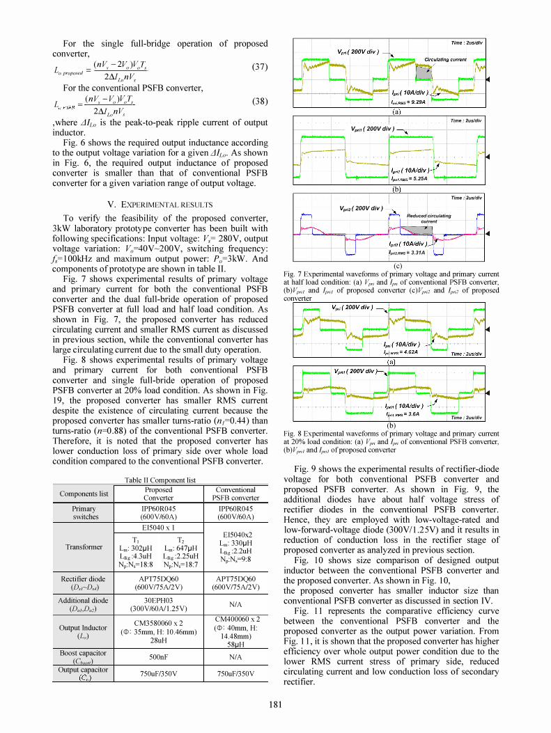
Fig. 7 shows experimental results of primary voltage and primary current for both the conventional PSFB converter and the dual full-bride operation of proposed PSFB converter at full load and half load condition. As shown in Fig. 7, the proposed converter has reduced circulating current and smaller RMS current as discussed in previous section, while the conventional converter has large circulating current due to the small duty operation.
Fig. S shows experimental results of primary voltage and primary current for both conventional PSFB converter and single full-bride operation of proposed PSFB converter at 20% load condition. As shown in Fig. 19, the proposed converter has smaller RMS current despite the existence of circulating current because the proposed converter has smaller turns-ratio (n]=0. 44) than turns-ratio (n=O. SS) of the conventional PSFB converter. Therefore, it is noted that the proposed converter has lower conduction loss of primary side over whole load condition compared to the conventional PSFB converter.
Table II Component list
Components list Proposed Conventional Converter PSFB converter
Primary IPP60R045 IPP60R045 switches (600Y/60A) (600Y/60A)
EI5040 x I EI5040x2
TI T2 Lm: 330[..lH Transformer Lm: 302[..1H Lm: 647[..1H Llkg :2.2uH Llkg :4.3uH Llkg :2.25uH Np:Ns=9:8 Np:Ns=18:8 Np:Ns=18:7
Rectifier diode APT75DQ60 APT75DQ60 (D>1-D,;) (600VI75A12V) (600VI75A12V)
Additional diode 30EPH03 N/A (DoJ,Do2) (300V/60Al1.25V)
CM3580060 x 2 CM400060 x 2 Output Inductor (ctJ: 35mm, H: 1O.46mm) (ctJ: 40mm, H:
(La) 14.48mm) 28uH 58[..1H Boost capacitor 500nF N/A ( Cboo")
Output capacitor 750uF/350V 750uF/350V (Ca)
lSI
a Time: 2us/d;v
V pri1 ( 200V div ) ---,. 1"-----.
--..... --..Il lpri' .RMS = 5.25A
V",i2( 200V div)
b
Reduced circulating current
rprl2.RMS = J.31A
(c)
Time: 2usldiv
Fig. 7 Experimental waveforms of primary voltage and primary current at half load condition: (a) Vpri and Ipr! of conventional PSFB converter, (b) Vpril and Ipril of proposed converter (c) Vpn2 and Ipn2 of proposed converter
'r".RMS;;; 3.6A (b)
Time: 2usJdiv
Fig. 8 Experimental waveforms of primary voltage and primary current at 20% load condition: (a) Vpri and Ipri of conventional PSFB converter, (b) Vpril and IpnJ of proposed converter
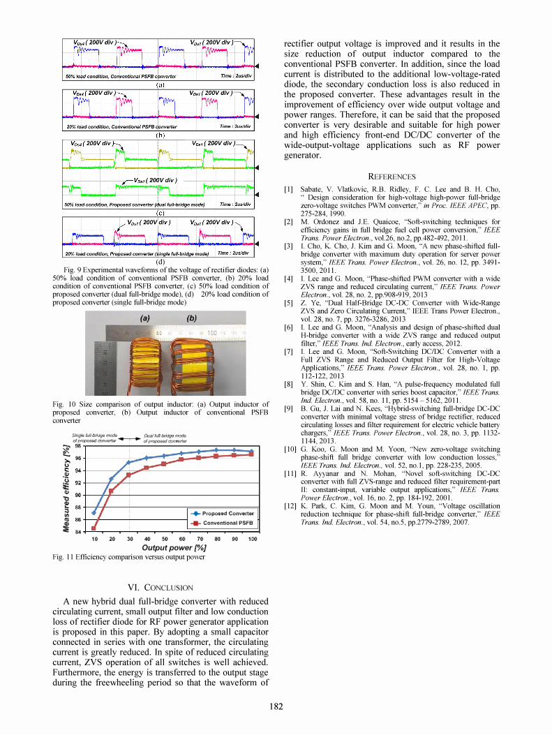
Fig. 9 shows the experimental results of rectifier-diode voltage for both conventional PSFB converter and proposed PSFB converter. As shown in Fig. 9, the additional diodes have about half voltage stress of rectifier diodes in the conventional PSFB converter. Hence, they are employed with low-voltage-rated and low-forward-voltage diode (300Vl1. 25V) and it results in reduction of conduction loss in the rectifier stage of proposed converter as analyzed in previous section.
Fig. 10 shows size comparison of designed output inductor between the conventional PSFB converter and the proposed converter. As shown in Fig. 10, the proposed converter has smaller inductor size than conventional PSFB converter as discussed in section IV.
Fig. I I represents the comparative efficiency curve between the conventional PSFB converter and the proposed converter as the output power variation. From Fig. 11, it is shown that the proposed converter has higher efficiency over whole output power condition due to the lower RMS current stress of primary side, reduced circulating current and low conduction loss of secondary rectifier.
(d) Fig. 9 Experimental waveforms of the voltage of rectifier diodes: (a)
50% load condition of conventional PSFB converter, (b) 20% load condition of conventional PSFB converter, (c) 50% load condition of proposed converter (dual full-bridge mode), (d) 20% load condition of proposed converter (single full-bridge mode)
(a) (b) ---_ ....
Fig. 10 Size comparison of output inductor: (a) Output inductor of proposed converter, (b) Output inductor of conventional PSFB converter
�=�=c:: � �::::��=! � 9
8I=========:C:::::::��::�:::;:;��;;iL] � 96 � � �+-------����------------------------�
.! � 92 +---���+---------------------------� � 90+---�F---�----------------------------� b � 88 +-.f�----�------------�--------------� ;;; -+- Proposed Converter � 86 +-��----�----------� � 84
--- Conventional PSFB
10 20 30 40 50 60 70 80 90 100 Output power [%}
Fig. 11 Efficiency comparison versus output power
VI. CONCLUSION
A new hybrid dual full-bridge converter with reduced circulating current, small output filter and low conduction loss of rectifier diode for RF power generator application is proposed in this paper. By adopting a small capacitor connected in series with one transformer, the circulating current is greatly reduced. In spite of reduced circulating current, ZVS operation of all switches is well achieved. Furthermore, the energy is transferred to the output stage during the freewheeling period so that the waveform of
182
rectifier output voltage is improved and it results in the size reduction of output inductor compared to the conventional PSFB converter. In addition, since the load current is distributed to the additional low-voltage-rated diode, the secondary conduction loss is also reduced in the proposed converter. These advantages result in the improvement of efficiency over wide output voltage and power ranges. Therefore, it can be said that the proposed converter is very desirable and suitable for high power and high efficiency front-end DCIDC converter of the wide-output-voltage applications such as RF power generator.
REFERENCES
[I] Sabate, V. V1atkovic, R.B. Ridley, F. C. Lee and B. H. Cho, " Design consideration for high-voltage high-power full-bridge zero-voltage switches PWM converter," in Froc. IEEE APEC, pp. 275-284, 1990.
[2] M. Ordonez and 1.E. Quaicoe, "Soft-switching techniques for efficiency gains in full bridge fuel cell power conversion," IEEE Trans. Power Electron., vo1.26, no.2, pp.482-492, 2011.
[3] I. Cho, K. Cho, 1. Kim and G. Moon, "A new phase-shifted fullbridge converter with maximum duty operation for server power system," IEEE Trans. Power Electron., vol. 26, no. 12, pp. 3491-3500,2011.
[4] I. Lee and G. Moon, "Phase-shifted PWM converter with a wide ZVS range and reduced circulating current," IEEE Trans. Power Electron., vol. 28, no. 2, pp.908-919, 2013
[5] Z. Ye, "Dual Half-Bridge DC-DC Converter with Wide-Range ZVS and Zero Circulating Current," IEEE Trans Power Electron., vol. 28, no. 7, pp. 3276-3286, 2013
[6] I. Lee and G. Moon, "Analysis and design of phase-shifted dual H-bridge converter with a wide ZVS range and reduced output filter," IEEE Trans. Ind. Electron., early access, 2012.
[7] I. Lee and G. Moon, "Soft-Switching DCfDC Converter with a Full ZVS Range and Reduced Output Filter for High-Voltage Applications," IEEE Trans. Power Electron., vol. 28, no. I, pp. 112-122, 2013
[8] Y. Shin, C. Kim and S. Han, "A pulse-frequency modulated full bridge DCfDC converter with series boost capacitor," IEEE Trans. Ind. Electron., vol. 58, no. 11, pp. 5154 - 5162, 2011.
[9] B. Gu, .I. Lai and N. Kees, "Hybrid-switching full-bridge DC-DC converter with minimal voltage stress of bridge rectifier, reduced circulating losses and filter requirement for electric vehicle battery chargers," IEEE Trans. Power Electron., vol. 28, no. 3, pp. 1132-1144,2013.
[10] G. Koo, G. Moon and M. Yoon, "New zero-voltage switching phase-shift full bridge converter with low conduction losses," IEEE Trans. Ind. Electron., vol. 52, no. I, pp. 228-235, 2005.
[11] R. Ayyanar and N. Mohan, "Novel soft-switching DC-DC converter with full ZVS-range and reduced filter requirement-part II: constant-input, variable output applications," IEEE Trans. Power Electron., vol. 16, no. 2, pp. 184-192,2001.
[12] K. Park, C. Kim, G. Moon and M. Youn, "Voltage oscillation reduction technique for phase-shift full-bridge converter," IEEE Trans. Ind. Electron., vol. 54, no.5, pp.2779-2789, 2007.